TDF1779A
April 1993
DUAL 2-A SOURCE DRIVER
.
OUTPUT CURRENT UP TO 2.5 A
.
WIDE RANGE OF SUPPLY VOLTAGE : + 8 V
TO + 26 V
.
CAN WITHSTAND OVERVOLTAGES OF AS
HIGH AS 60 V BETWEEN V
CC
AND GROUND
.
OUTPUT VOLTAGE CAN SWING TO LOWER
THAN GROUND
.
"SENSE" AND "ALARM" OUTPUTS ARE OPEN
COLLECTOR OUTPUTS
DESCRIPTION
The TDF1779A is a dual source driver delivering
hihg outputcurrents and the capabilityto drive highly
inductive loads (Electrovalves, contractors, re-
lays...).
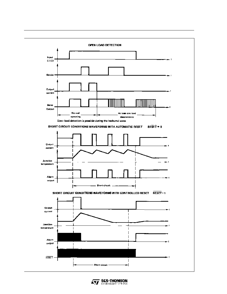
This device is essentially blow-out proof, each out-
put is protected against short-circuits. If internal dis-
sipation becomes too high, drivers will shut down to
prevent excessive heating. An "ALARM" output is
provided to indicate the action of the thermal protec-
tion. To reactivate the power outputs, the reset input
must be forced to low state.
"SENSE" information of both power outputs are
ORed together and then processed internally.
A "STROBE" input is also provided to offer the pos-
sibility of disabling the power outputs.
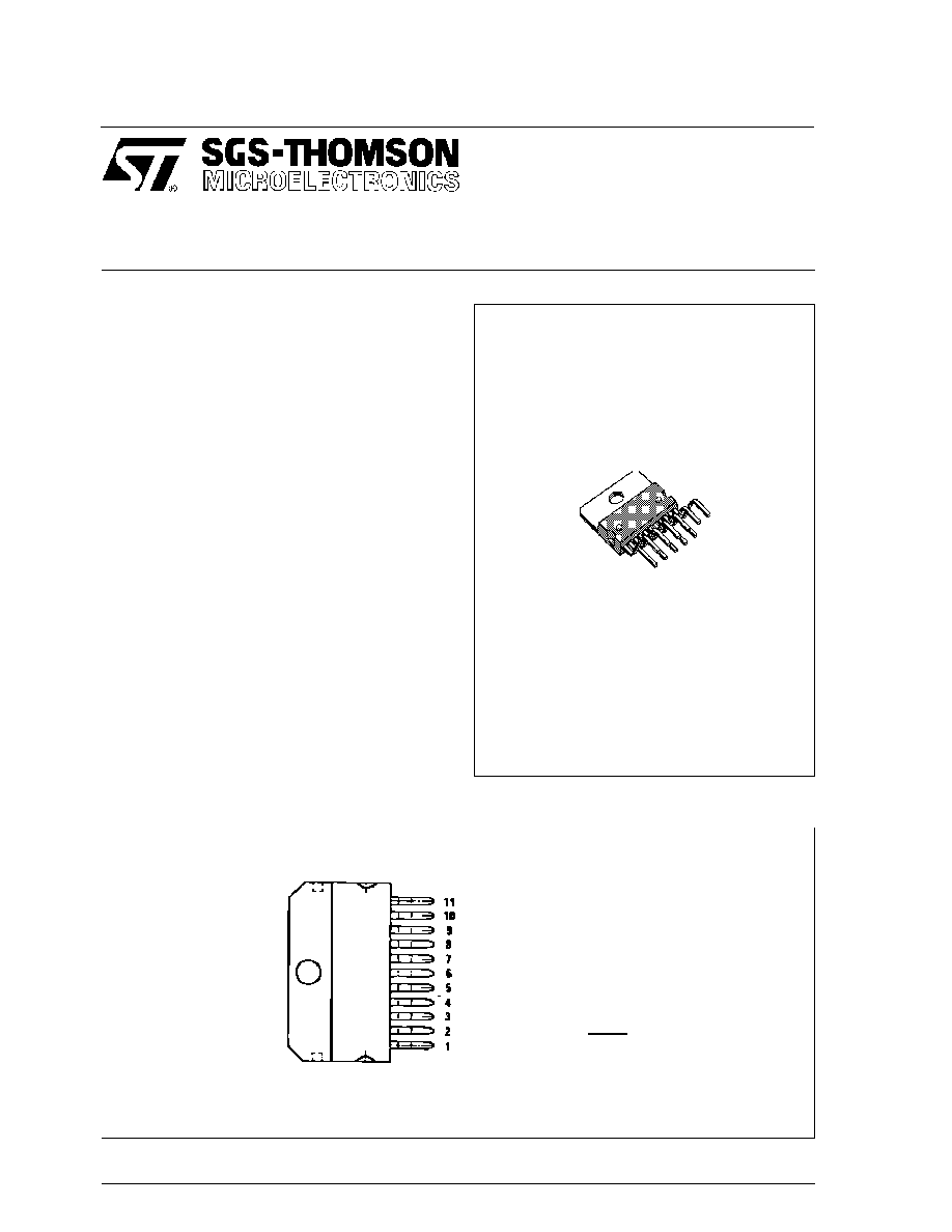
MULTIWATT-11
ORDERING NUMBER : TDE 1779ASP
Tab is connected to pin 6
1 - Output 1
2 - V
CC
3 - Output 2
4 - N.C.
5 - Strobe
6 - Ground
7 - Input 2
8 - Sense output
9 - Alarm output
10 - Reset input
11 - Input 1
PIN CONNECTION
1/9

BLOCK DIAGRAM
MAXIMUM RATINGS
Symbol
arameter
Value
Unit
V
CC
Supply Voltage
35 V (60 V/10 ms)
V
V
I
, V
reset
Input Voltage (Pins 7, 10 and 11)
≠ 30 to + 50
V
V
strobe
Strobe Input Voltage
≠ 0.5 to V
CC
V
I
O
Output Current
Internally Limited
A
P
tot
Power Dissipation
Internally Limited
W
T
oper
Operating Ambient temperature Range
≠ 40 to + 85
∞
C
THERMAL CHARACTERISTICS
Symbol
Parameter
Value
Uni
R
th (j-c)
Junction-case Thermal Resistance
Max.
3
∞
C/W
R
th (j-a)
Junction-ambient Thermal Resistance
Max.
40
∞
C/W
TDF1779A
2/9

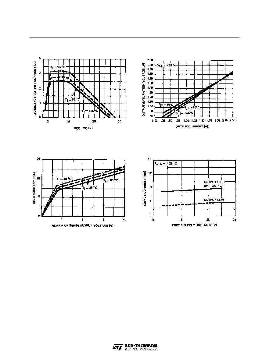
ELECTRICAL OPERATING CHARACTERISTICS
(V
CC
= + 24V, ≠40
o
C < T
j
< + 85
o
C, unless otherwise specified)
Symbol
Parameter
Min.
Typ.
Max.
Unit
V
CC
Power Supply Voltage
8
-
26
V
I
CC
Power Supply Current (pin 6), I
O1
=I
O2
= 2A
-
-
20
mA
V
IL
V
IH
Logic Input Voltage (pin 7,10,11)
-
2
-
-
0.8
-
V
V
I
Logic Input Threshold (pin 5)
-
0.8
-
V
I
IH
High Level Input Current (pins 7,10,11) V
I
= + 2V
-
20
50
µ
A
I
IL
Low Level Input Current (pins 7,10,11) V
I
= + 0.8V
≠ 5
0
+ 5
µ
A
-
Off State Output Voltage (pins 8,9) |(8) = |(9) = 2 mA
-
-
0.4
V
V
CC
≠ V
01
V
CC
≠ V
02
Output Saturation Voltage (V(7) high, V(11) High, I
O
= 2A)
-
1.5
1.8
V
I
OL
Low Level Output Current pins 1,3)
V(7) Low, V(11) Low, V
O
= 0V
-
400
1000
µ
A
V
CC
≠ V
01
V
CC
≠ V
02
Switch-off Output Voltage (inductive load) Note 1
-
-
45
V
I
O
1, I
O2
Available Ouptut Current (pins 1,3), V(7) high, V(11p) high,
V
CC
≠ V
O
= 26V, T
j
= 25
∞
C
10
-
-
mA
I
O Alarme
Available "Alarme" Output Current, V(9) = + 4V
4
8
-
mA
I
O Sense
Available "Sense Ouptut Current, V(8) = + 4V
4
8
-
mA
I
IH Sense
Output Sensing high Level Input Current (pins 1,3) V
I
= +2V
-
1
2
mA
Note 1 : An external discharge circuit is required for inductive loads
TDF1779A
3/9