
TEA2262
SWITCH MODE POWER SUPPLY CONTROLLER
April 1996
1
2
3
4
5
6
7
8
16
15
14
13
12
11
10
9
IS
IN
GND
GND
E
S
SECONDARY PULSES INPUT
GROUND
GROUND
ERROR AMPLIFIER INPUT (INVERTING)
ERROR AMPLIFIER OUTPUT
OVERLOAD INTEGRATION CAPACITOR
POWER SUPPLY
POSITIVE OUTPUT STAGE SUPPLY
POWER OUTPUT
GROUND
GROUND
OSCILLATOR RESISTOR
OSCILLATOR CAPACITOR
SOFT-START CAPACITOR
V
V
OUT
GND
GND
C0
C1
R0
CC
max.
I
C2
TRANSFORMER DEMAGNETIZATION
SENSING INPUT
POWER TRANSISTOR
CURRENT LIMITATION INPUT
2262-01.EPS
PIN CONNECTIONS
DIP16
(Plastic Package)
ORDER CODE : TEA2262
.
POSITIVE AND NEGATIVE OUTPUT CUR-
RENT UP TO 1A
.
LOW START-UP CURRENT
.
DIRECT DRIVE OF THE MOS POWER
TRANSISTOR
.
TWO LEVELS TRANSISTOR CURRENT LIMI-
TATION
.
DOUBLE PULSE SUPPRESSION
.
SOFT-STARTING
.
UNDER AND OVERVOLTAGE LOCK-OUT
.
AUTOMATIC STAND-BY MODE
.
LARGE POWER RANGE CAPABILITY IN
STAND-BY (Burst mode)
.
INTERNAL PWM SIGNAL GENERATOR
DESCRIPTION
The TEA2262 is a monolithic integrated circuit for
the use in primary part of an off-line switching mode
power supply using a MOS power transistor.
All functions required for SMPS control under nor-
mal operating, transient or abnormal conditions are
provided.
The capability of working according to the "master-
slave" concept, or according to the "primary regu-
lation" mode makes the TEA2262 very flexible and
easy to use. This is particularly true for TV receiv-
ers where the IC provides an attractive and low cost
solution (no need of stand-by auxiliary power sup-
ply).
1/9
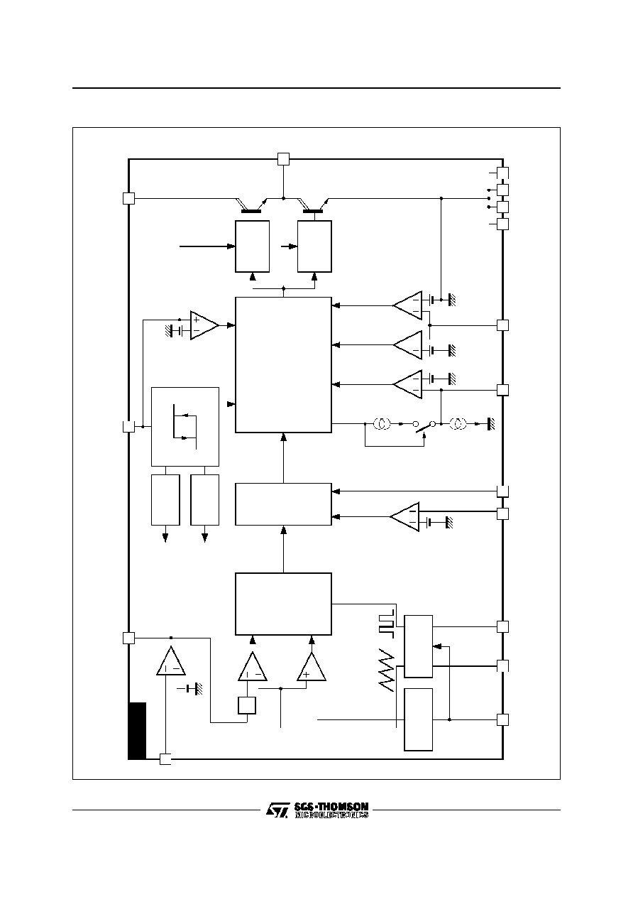
INTERNAL
BIAS
V
REF
(2.49V)
AUTOMATIC
BURST
GENERATION
12
3
4
5
6
7
8
91
0
16
11
12
13
14
POSITIVE
OUTPUT
STAGE
NEGATIVE
OUTPUT
STAGE
V
CC
+1A
(Max.)
-1A
(Max.)
OUT
45
�
A
10
�
A
Secondary
Pulse
2.55V
0.6V
0.84V
Current
Limitation
Repetitive
Overload
Protection
LOGIC
PROCESSOR
15.7V
15
V+
Overvoltage
Protection
IS
LOGIC
0.15V
GND
I
MAX
C
2
IN
IS
Regulation
Pulses
Primary
Pulses
V
CC
MONITORING
8.5V
11.8V
V
CC
MODULATOR
LOGIC
Demagnetization
Sensing
Modulators
-1
OSCILLATOR
f/4
T
ON
(Max.)
(60%)
SOFT-START
C
0
R
0
C
1
V
REF
2.49V
Error
Amplifier
S
E
TEA2262
2262-02.EPS
BLOCK DIAGRAM
TEA2262
2/9
ABSOLUTE MAXIMUM RATINGS
Symbol
Parameter
Value
Unit
V
CC
Power Supply
V16-V4, 5, 12, 13
20
V
V+
Output Stage Power Supply
V15-V4, 5, 12, 13
20
V
I
OUT
+
Positive Output Current (source current)
1.5
A
I
OUT
-
Negative Output Current (sink current)
1.5
A
T
j
Operating Junction Temperature
150
o
C
T
stg
Storage Temperature
-40, +150
o
C
2262-01.TBL
THERMAL DATA
Symbol
Parameter
Value
Unit
R
th (j-c)
Junction-case Thermal Resistance
15
o
C/W
R
th (j-a)
*
Junction-ambient Thermal Resistance
50
o
C/W
* Soldered on a 35
�
m, 40cm
2
board copper area
2262-02.TBL
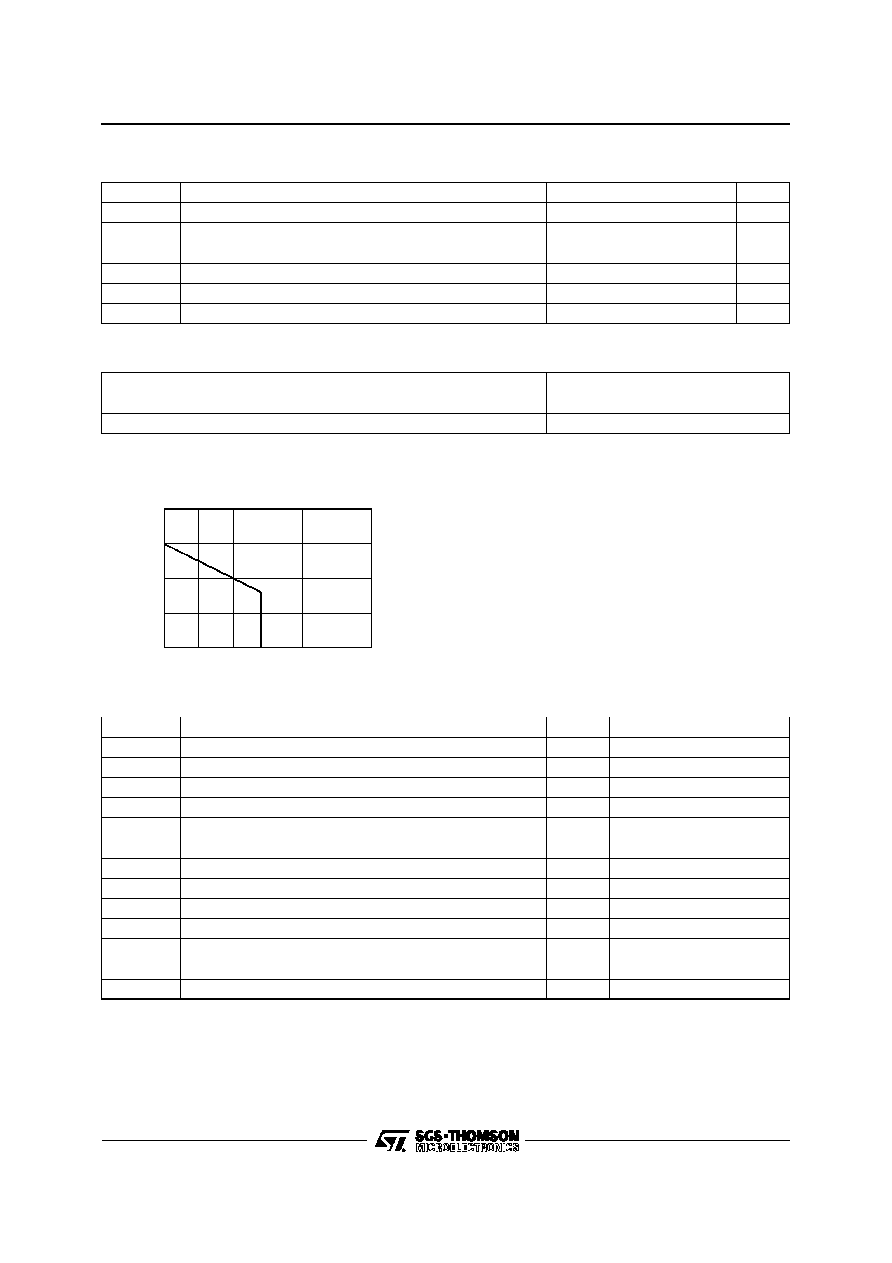
50
100
150
0
3
2
1
P
(W)
tot
4
T
( C)
AMB
o
o
50 C/W
2262-03.EPS
Figure 1 : Maximum Power Dissipation
RECOMMENDED OPERATING CONDITIONS
Symbol
Parameter
Min.
Typ.
Max.
Unit
V
CC
Power Supply
V
CC
stop
12
V
CC
max
V
I
OUT
+
Positive Output Current (source current)
1
A
I
OUT
-
Negative Output Current (sink current)
1
A
I
OUT
+
Average Positive Output Current
0.3
A
I
OUT
-
Average Negative Output Current
0.3
A
f
oper
Operating Frequency
10
150
kHz
V
IN
Input Pulses Amplitude (Pin 2)
1.5
2.5
4.5
V
R
OSC
Oscillator Resistor Range
10
100
k
C
OSC
Oscillator Capacitor Range
0.33
4.7
nF
C1
Soft-starting Capacitor Range
0.047
1
�
F
C2
Overload Integration Capacitor
0.047
1
�
F
C2/C1
Ratio C2/C1 (C2 must be
C1)
1
T
amb
Operating Ambient Temperature
-20
70
o
C
2262-03.TBL
TEA2262
3/9
ELECTRICAL CHARACTERISTICS (T
amb
= 25
o
C, V
CC
=12V, unless otherwise specified)
Symbol
Parameter
Min.
Typ.
Max.
Unit
POWER SUPPLY
V
CC(start)
Starting Voltage (V
CC
increasing)
9.5
11.8
13
V
V
CC(stop)
Stopping Voltage (V
CC
decreasing)
7
8.5
9.5
V
Hyst V
CC
Hysteresis (V
CC(start)
- V
CC(Stop)
)
2.7
3.3
3.7
V
I
CC(start)
Starting Current (V
CC
= 9V)
0.5
mA
I
CC
Supply Current (V
CC
= 12V)
6.5
mA
V
CC(max)
Overvoltage Threshold on V
CC
15
15.7
V
I
CC(over)
Supply Current after Overvoltage Detection (V
CC
= 17V)
35
mA
OSCILLATOR / PWM SECTION
F
F
Accuracy (R
OSC
= 68k
, C
OSC
= 1nF)
10
%
t
ON
max
Maximum Duty Cycle in Primary Regulation Mode
50
60
70
%
ERROR AMPLIFIER SECTION
A
VO
Open Loop Gain
75
dB
F
ug
Unity Gain Frequency
550
kHz
I
SC
Short Circuit Output Current (Pin 7 connected to ground)
2
mA
I
BE
E Input Bias Current (Pin 6)
0.08
�
A
V
REF
Internal Voltage Reference
(connected to error amplifier input and not directly accessible)
2.34
2.49
2.64
V
INPUT SECTION
V
IN
IN Input Threshold (Pin 2)
0.6
0.85
1.2
V
V
IS
IS Input Threshold (Pin 1)
0.15
V
I
BIN
IN Input Bias Current
0.3
�
A
I
BIS
IS Input Bias Current
0.4
�
A
CURRENT LIMITATION SECTION
V
IM1
First Current Limitation Threshold
550
600
650
mV
V
IM2
Second Current Limitation Threshold
780
840
900
mV
V
IM
Thresholds Difference V
IM2
- V
IM1
190
240
280
mV
V
C2
Lock-out Threshold on Pin C2
2.25
2.55
2.85
V
I
DC2
Capacitor C2 Discharge Current
10
�
A
I
CC2
Capacitor C2 Charge Current
45
�
A
I
BI(max)
Maximum Input Bias Current (Pin 3)
0.2
�
A
2262-04.TBL
TEA2262
4/9

AUDIO
OUTPUT
STAGE
SCANNING
DEVICE
MAINS
INPUT
R
C
VOLTAGE
REGULATOR
�
P
INFRA-RED
RECEIVER
Muting
Control
Remote
Stand-by
Remote
Stand-by
Synchronization
V
CC
2
P
P
1
V
CC
2
1
P
: Output voltage adjusteme nt in normal mode
P : Output voltage adjuste ment in stand- by
Power primary ground
Secondary ground (isolated from mains)
PWM
TEA5170
MASTER
TEA2262
SLAVE
2262-04.EPS
Figure 1 : Master-slave Concept
AUDIO
OUTPUT
STAGE
SCANNING
DEVICE
MAINS
INPUT
R
C
VOLTAGE
REGULATOR
�
P
INFRA-RED
RECEIVER
Muting
Control
Remote
Stand-by
V
CC
P
V
CC
P : Output voltage adjustement
Power primary ground
Secondary ground (isolated from mains)
TEA2262
2262-05.EPS
Figure 2 : Secondary Regulation (with optocoupler)
SIMPLIFIED APPLICATION DIAGRAMS
TEA2262
5/9

GENERAL DESCRIPTION
The TEA2262 is an off-line switch mode power
supply controller. The synchronization function and
the specific operation in stand-by mode make it well
adapted to video applications such as TV sets,
VCRs, monitors, etc...
The TEA2262 can be used in two types of architec-
tures :
- Master/slave architecture. In this case, the
TEA2262drives the power transistor according to
the pulse width modulated signals generated by
the secondary located master circuit. A pulse
transformer provides the feedback(see Figure 1).
- Conventional architecture with linear feedback
signal (feedback sources : optocoupler or trans-
former winding) (see Figure 2).
Using the TEA2262, the stand-by auxiliary power
supply, often realized with a small but costly 50Hz
transformer, is no longer necessary. The burst
mode operation of the TEA2262 makes possible
the control of very low output power (down to less
than 1W) with the main power transformer.
When used in a master/slave architecture, the
TEA2262 and also the power transistor turn-off can
be easily synchronized with the line transformer.
The switching noise cannot disturb the picture in
this case.
As an S.M.P.S. controller, the TEA2262 features
the following functions :
- Power supply start-up (with soft-start)
- PWM generator
- Direct power transistor drive (
�
1A)
- Safety functions : pulse by pulse current limita-
tion, output power limitation, over and under volt-
age lock-out.
S.M.P.S. OPERATING DESCRIPTION
Starting Mode - Stand By Mode
Power for circuit supply is taken from the mains
through a high value resistor before starting. As
long as V
CC
of the TEA2262 is below V
CC
start, the
quiescent current is very low (typically 0.5mA) and
the electrolytic capacitor across V
CC
is linearly
charged. When V
CC
reaches V
CC
start (typically
11.8V), the circuit starts, generating output pulses
with a soft-starting. Then the SMPS goes into the
stand-by mode and the output voltage is a percen-
tage of the nominal output voltage (eg. 80%).
During starting phase, in order to avoid transformer
magnetization (specially at high frequency), the
frequency oscillator is divided by four.
At switch-on, C
0
charging current is divided by four.
It recover its normal value when the voltage on
soft-start capacitor reach 2.5V.
The current also recover its standard value when
the soft-start capacitor is discharged because of a
burst operating mode (starting in stand-by).
In other words, the charging current will become
and stay at its normal value, as soon as one of the
following events occurs :
- V
C1
rearch 2.5V
- C
1
is discharged by burst operating mode
For this the TEA2262 contains all the functions
required for primary mode regulation : a fixed fre-
quency oscillator, a voltage reference, an error
amplifier and a pulse width modulator (PWM).
For transmission of low power with a good effi-
ciency in stand-by, an automatic burst generation
system is used, in order to avoid audible noise.
Normal Mode (secondary regulation)
The normal operating of the TV set is obtained by
sending to the TEA2262 regulation pulses gener-
ated by a regulator located in the secondary side
of the power supply (TEA5170 for example).
This architecture uses the "Master-slave Concept",
advantages of which are now well-known espe-
cially the very high efficiency in stand-bymode, and
the accurate regulation in normal mode.
Stand-by mode or normal mode are obtained by
supplying or not the secondary regulator. This can
be ordonnered for exemple by a microprocessor in
relation with the remote control unit.
Regulation pulses are applied to the TEA2262
through a small pulse-transformer to the IN input
(pin 2). This input is sensitive to positive square
pulses. The typical threshold of this input is 0.85V.
The frequency of pulses coming from the secon-
dary regulator can be lower or higher than the
frequency of the starting oscillator.
The TEA2262 has no soft-starting system when it
receives pulses from the secondary. The soft-start-
ing has to be located in the secondary regulator.
Due to the principle of the primary regulation,
pulses generated by the starting system automat-
ically disappear when the voltage delivered by the
SMPS increases.
TEA2262
6/9

Stand-by Mode - Normal Mode Transition
During the transition there are simultaneously
pulses coming from the primary and secondary
regulators.
These signals are not synchronized and some care
has to be taken to ensure the safety of the switching
power transistor.
A very sure and simple way consist in checking the
transformer demagnetization state.
- A primary pulse is taken in account only if the
transformer is demagnetized after a conduction
of the power transistor required by the secondary
regulator.
- A secondary pulse is taken in account only if the
transformer is demagnetized after a conduction
of the power transistor required by the primary
regulator.
With this arrangement the switching safety area of
the power transistor is respected and there is no
risk of transformer magnetization.
The magnetization state of the transformer is
checked by sensing the voltage across a winding
of the transformer (generally the same which sup-
plies the TEA2262). This is made by connecting a
resistor between this winding and the demagneti-
zation sensing input of the circuit (pin 1).
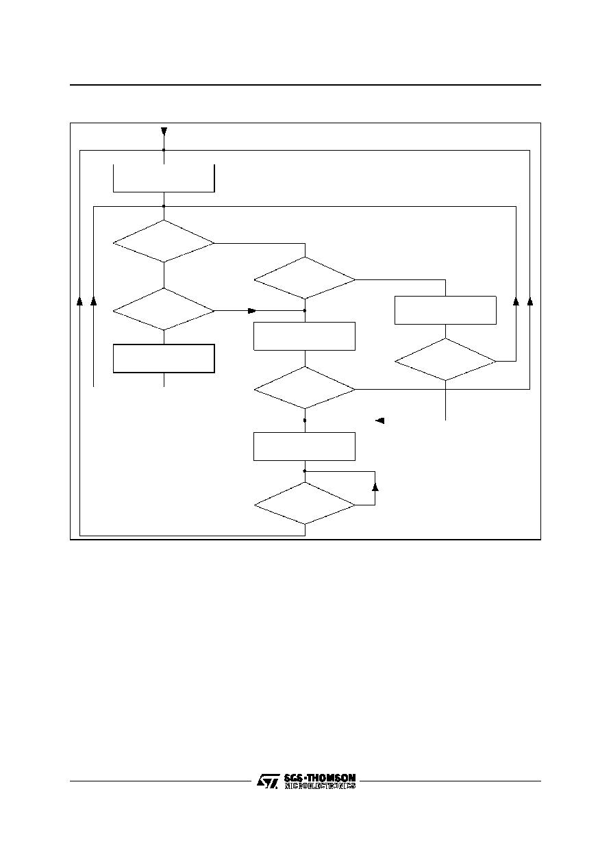
SECURITY FUNCTIONS (see flow-chart below)
- Undervoltage detection. This protection works
in association with the starting device "V
CC
switch" (see paragraph Starting-mode - standby
mode). If V
CC
is lower than V
CC
stop (typically
8.5V) output pulses are inhibited, in order to avoid
wrong operation of the power supply or bad
power transistor drive.
- Overvoltage detection. If V
CC
exceeds V
CC
max
(typically 15.7V) output pulses are inhibited and
the external capacitor C
2
is charged as long as
V
CC
is higher than V
CC
stop. Restarting of the
power supply is obtained by reducing V
CC
below
V
CC
stop except if the voltage across C
2
reaches
V
C2
(typically 2.55V) (refer to "Restart of the
power supply" paragraph).In this last case, the
circuit is definitively stopped.
- Current limitation of the power transistor. The
current is measured by a shunt resistor. A double
threshold system is used :
- When the first threshold (V
IM1
) is reached, the
conduction of the power transistor is stopped
until the end of the period : a new conduction
signal is needed to obtain conduction again.
- Furthermore as long as the first threshold is
reached (it means during several periods), an
external capacitor C
2
is charged. When the
voltage across the capacitor reaches V
C2
(typi-
cally 2.55V) the output is inhibited. This is called
the "repetitive overload protection". If the over-
load diseappears before V
C2
is reached, C
2
is
discharged, so transient overloads are toler-
ated.
- Second current limitation thresho ld (V
IM2
).
When this threshold is reached the output of the
circuit is immediatly inhibited. This protection is
helpfull in case of hard overload for example to
avoid the magnetization of the transformer.
- Restart of the power supply. After stopping due
to V
IM2
, V
CC
Max or V
CC
stop triggering, restart of
the power supply can be obtained by the normal
operating of the "V
CC
switch" V
CC
switch se-
quency from V
CC
stop to V
CC
start . After stopping
due to V
C2
threshold reaching, the circuit is de-
finitively stopped. In this case it is necessary to
reduce V
CC
below approximately 5V to reset the
circuit. From a practical point of view, it means
that the power supply has to be temporarily dis-
connected from any power source to get the
restart.
TEA2262
7/9
S.M.P.S.
starting
First
threshold reached
VIM1
2
V
< 2.6V
C2
CC
V
max
reached
2
Normal operating
C discharged
Definitive
stopping
N
N
Y
N
N
Y
Y
Y
N
Y
Pulse by pulse current
limiting C charged
2
C charged
S.M.P.S. stopped
V
< 2.6V
C2
Y
Reset C
discharged
2
N
Second
threshold reached
VIM2
2262-06.EPS
SECURITY FLOW-CHART
TEA2262
8/9
PM-DIP16.EPS
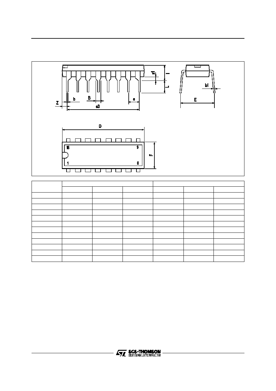
PACKAGE MECHANICAL DATA
16 PINS - PLASTIC DIP
Information furnished is believed to be accurate and reliable. However, SGS-THOMSON Microelectronics assumes no responsibility
for the consequences of use of such information nor for any infringement of patents or other rights of third parties which may result
from its use. No licence is granted by implication or otherwise under any patent or patent rights of SGS-THOMSON Microelectronics.
Specifications mentioned in this publication are subject to change without notice. This publication supersedes and replaces all
information previously supplied. SGS-THOMSON Microelectronics products are not authorized for use as critical components in life
support devices or systems without express written approval of SGS-THOMSON Microelectronics.
�
199 SGS-THOMSON Microelectronics - All Rights Reserved
Purchase of I
2
C Components of SGS-THOMSON Microelectronics, conveys a license under the Philips
I
2
C Patent. Rights to use these components in a I
2
C system, is granted provided that the system conforms to
the I
2
C Standard Specifications as defined by Philips.
SGS-THOMSON Microelectronics GROUP OF COMPANIES
Australia - Brazil - Canada - China - France - Germany - Hong Kong - Italy - Japan - Korea - Malaysia - Malta - Morocco
The Netherlands - Singapore - Spain - Sweden - Switzerland - Taiwan - Thailand - United Kingdom - U.S.A.
Dimensions
Millimeters
Inches
Min.
Typ.
Max.
Min.
Typ.
Max.
a1
0.51
0.020
B
0.77
1.65
0.030
0.065
b
0.5
0.020
b1
0.25
0.010
D
20
0.787
E
8.5
0.335
e
2.54
0.100
e3
17.78
0.700
F
7.1
0.280
I
5.1
0.201
L
3.3
0.130
Z
1.27
0.050
DIP16.TBL
TEA2262
9/9