TEA3718
TEA3718S
STEPPER MOTOR DRIVER
ADVANCE DAT A
HALF-STEP AND FULL-STEP MODE
BIPOLAR DRIVE OF STEPPER MOTOR FOR
MAXIMUM MOTOR PERFORMANCE
BUILT-IN PROTECTION DIODES
WIDE RANGE OF CURRENT CONTROL 5 TO
1500 mA
WIDE VOLTAGE RANGE 10 TO 50 V
DESIGNED FOR UNSTABILIZED MOTOR
SUPPLY VOLTAGE
CURRENT LEVELS CAN BE SELECTED IN
STEPS OR VARIED CONTINUOUSLY
THERMAL OVERLOAD PROTECTION
ALARM OUTPUT OR PRE-ALARM OUTPUT
(see internal table)
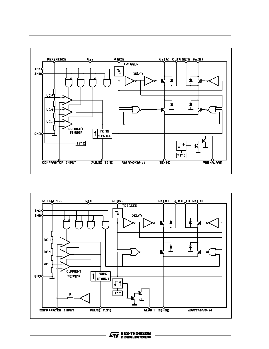
DESCRIPTION
The TEA3718 and TEA3718Sare bipolar monolithic
integrated circuits intended to control and drive the
current in one winding of a bipolar stepper motor.
The circuits consist of an LS-TTL compatible logic
input, a current sensor, a monostable and an output
stage with built-in protection diodes. Two TEA3718
or TEA3718S and a few external components form
a complete control and drive unit for LS-TTL or mi-
croprocessor-controlled stepper motor systems.
Powerdip
12 + 2 + 2
MULTIWA TT-15
TEA3718SP
(Multiwatt-15)
TEA3718SFP
(SO-20)
TEA3718DP
TEA3718SDP
(Powerdip 12+2+2)
PIN CONNECTIONS (top views)
ORDERING NUMBERS :
TEA3718SDP
TEA3718DP
ORDERING NUMBER : TEA3718SP
1/16
This is advanced information on a new product now in development or undergoing evaluation. Details are subject to change without notice.
SO-20
ORDERING NUMBER :
TEA3718SFP
December 1991

PIN FUNCTIONS
Name
Fu nctio n
OUT B
Output Connection (with pin OUTA). The output stage is a "H" bridge formed by four
transistors and four diodes suitable for switching applications.
PULSE TIME
A parallel RC network connected to this pin sets the OFF time of the lower power
transistors. The pulse generator is a monostable triggered by the rising edge of the
output of the comparators (t
off
= 0.69 R
T
C
T
).
V
S
(B)
Supply Voltage Input for Half Output Stage
GND
Ground Connection. In SO-20L and Powerdip these pins also conduct heat from die
to printed circuit copper.
V
SS
Supply Voltage Input for Logic Circuitry
IN1
This pin and pin IN0 are logic inputs which select the outputs of three comparators to
set the current level. Current also depends on the sensing resistor and reference
voltage. See truth table.
PHASE
This TTL-compatible logic input sets the direction of current flow through the load. A
high level causes current to flow from OUT A (source) to OUT B (sink). A Schmitt
trigger on this input provides good noise immunity and a delay circuit prevents output
stage short circuits during switching.
IN0
See INPUT 1
COMPARATOR INPUT
Input connected to the three comparators. The voltage across the sense resistor is
feedback to this input through the low pass filter R
C
C
C
. The lower power transistor
are disabled when the sense voltage exceeds the reference voltage of the selected
comparator. When this occurs the current decays for a time set by R
T
C
T
, T
off
= 0.69
R
T
C
T
.
REFERENCE
A voltage applied to this pin sets the reference voltage of the three comparators.
Reference voltage with the value of R
S
and the two inputs IN0 and IN1 determines
the output current.
V
S
(A)
Supply voltage input for half output stage
OUT A
See pin OUT B
SENSE RESISTOR
Connection to lower emitters of output stage for insertion of current sense resistor
ALARM
When T
j
reaches T1
�
C the alarm output becomes low (TEA3718SP)
PRE-ALARM
When T
j
reaches T2
�
C the prealarm output becomes low (T2<T1) (TEA3718SFP)
TEA3718-TEA3718S
3/16

ABSOLUTE MAXIMUM RATINGS
Symbol
Parameters
Valu e
Un it
V
SS
V
S
Supply Voltage
7
50
V
V
V
I
Input Voltage:
Logic Inputs
Analog Inputs
Reference Input
6
V
SS
15
V
V
V
i
i
Input Current
Logic Inputs
Analog Inputs
-10
-10
mA
mA
I
O
Output Current
�
1.5
A
T
J
Junction Temperature
+150
�
C
T
op
Operating Ambient Temperature Range
0 to 70
�
C
T
stg
Storage Temperature Range
-55 to +150
�
C
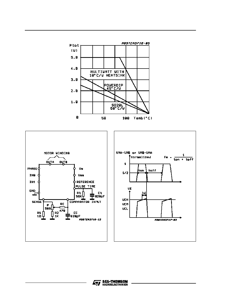
THERMAL DATA
Symb ol
Parameter
SO -20L
Po werdi p Mu lt iwatt
Uni t
R
th
(j-c)
Maximum Junction-case Thermal Resistance
16
11
3
�
C/W
R
th
(j-a)
Maximum Junction-ambient Thermal Resistance
60 *
45 *
40
�
C/W
* Soldered on a 35
�
m thick 4 cm
2
PC board copper area.
RECOMMENDED OPERATING CONDITIONS
Symb ol
Parameter
Min .
T yp.
Max.
Uni t
v
ss
Supply Voltage
4.75
5
5.25
V
V
S
Supply Voltage
10
�
45
V
i
m
Output Current
0.020
�
1.2
A
T
amb
Ambient Temperature
0
70
�
C
t
r
Rise Time Logic Inputs
�
�
2
�
s
t
f
Fall Time Logic Inputs
�
�
2
�
s
COMPARISON TABLE
Devi ce
Current
Package
Alarm
Pre-Al arm
TEA3718SDP
1.5A
Powerdip 12+2+2
not connected
TEA3718SFP
1.5A
SO-20L
x
TEA3718SP
1.5A
Multiwatt-15
X
TEA3718DP
1.5A
Powerdip 12+2+2
not connected
TEA3718-TEA3718S
4/16