
TEA6415C
BUS-CONTROLLED VIDEO MATRIX SWITCH
January 1996
s
20MHz BANDWIDTH
s
CASCADABLE WITH ANOTHER TEA6415C
(INTERNAL ADDRESS CAN BE CHANGED BY
PIN 7 VOLTAGE)
s
8 INPUTS (CVBS, RGB, MAC, CHROMA, ...)
s
6 OUTPUTS
s
POSSIBILITY OF MAC OR CHROMA SIGNAL
FOR EACH INPUT BY SWITCHING-OFF THE
CLAMP WITH AN EXTERNAL RESISTOR
BRIDGE
s
BUS CONTROLLED
s
6.5dB GAIN BETWEEN ANY INPUT AND OUT-
PUT
s
-55dB CROSSTALK AT 5MHz
s
FULLY ESD PROTECTED
DESCRIPTION
The main function of the TEA6415C is to switch 8
video input sources on the 6 outputs.
Each output can be switched to only one of the
inputs whereas but any same input may be con-
nected to several outputs.
All the switching possibilities are controlled through
the I
2
C bus.
DIP20
(Plastic Package)
ORDER CODE : TEA6415C
1
2
3
4
5
6
7
8
9
10
20
19
18
17
16
15
14
13
12
11
INPUT
DATA
CLOCK
PR OG
INPUT
INPUT
INPUT
INPUT
INPUT
INPUT
GROUND
OUTPUT
INPUT
OUTPUT
OUTPUT
OUTPUT
OUTPUT
OUTPUT
V
C C
GROUND
6415C-01.EPS
PIN CONNECTIONS
SO20
(Plastic Micropackage)
ORDER CODE : TEA6415CD
1/10

9
19
18
1 7
16
15
1 4
13
12
1
3
5
6
8
10
11
20
2
7
4
BUS
DECODER
DATA
GND
CLOCK
V
CC
TTX
LUMA
CHROMA
P OWER
PIP
MAC
DEC.
GND
CVBS
(AM TUNER)
MAC S IGNAL
(AMTUNER)
CVBS
(FM TUNER)
MAC S IGNAL
(FM TUNER)
S YNCHRO
(TTX/BTX)
P ERI
TV1
P ER I
TV2
CVBS
(P ER I P LUG2)
P ROG
CVBS
(P ER I P LUG1)
CVBS
(MAC/DEC)
T
E
A
6
4
1
5
C
6415C-02.EPS
BLOCK DIAGRAM
The main function of the IC is to switch 8 video input
sources on 6 outputs.
Each output can be switched on only one of each
input. On each input an alignment of the lowest
level of the signal is made (bottom of synch. top for
CVBS or black level for RGB signals).
Each nominal gain between any input and output
is 6.5dB. For D2MAC or Chroma signal the align-
ment is switched off by forcing, with an external
resistor bridge, 5 V
DC
on the input. Each input can
be used as a normal input or as a MAC or Chroma
input (with external resistor bridge). All the switch-
ing possibilities are changed through the BUS.
Driving 75
load needs an external transistor.
It is possible to have the same input connected to
several outputs.
The starting configuration upon power on (power
supply : 0 to 10V) is undetermined.
In this case, 6 words of 16 bits are necessary to
determine one configuration. In other case, 1 word
of 16 bits is necessary to determine one configura-
tion.
GENERAL DESCRIPTION
TEA6415C
2/10

ABSOLUTE MAXIMUM RATINGS
Symbol
Parameter
Value
Unit
V
CC
Supply Voltage (Pin 9)
12
V
T
A
Operating Ambient Temperature
0, +70
o
C
T
stg
Storage Temperature
- 20, +150
o
C
6415C-01.TBL
THERMAL DATA
Symbol
Parameter
Value
Unit
R
th(j-a)
Junction-Ambient Thermal Resistance
DIP20
SO20
80
100
o
C/W
o
C/W
6415C-02.TBL
ELECTRICAL CHARACTERISTICS
T
A
= 25
o
C , V
CC
= 10V , R
LOAD
= 10k
, C
LOAD
= 3pF (unless otherwise specified)
Symbol
Parameter
Min.
Typ.
Max.
Unit
V
CC
Supply Voltage (Pin 9)
8
10
11
V
I
CC
Power Supply Current (without load on outputs ; V
CC
=10V)
20
30
40
mA
INPUTS
Signal Amplitude (CVBS signal)
2
V
PP
Input Current (per output connected, input voltage = 5V
DC
)
(this current is X6 when all outputs are connected on the input)
1
3
�
A
DC Level
3.3
3.6
3.9
V
DC Level Shift (temperature from 0 to 70
o
C)
5
100
mV
OUTPUTS (V
IN
= 1V
PP
for all dynamic tests) Pins 13 - 14 - 15 - 16 - 17 - 18
Dynamic
4.5
5.5
V
PP
Output Impedance
25
50
Gain
6
6.5
7
dB
Bandwidth
-1dB attenuation
-3dB attenuation
7
15
20
MHz
MHz
Crosstalk
f = 5MHz
f = 3.58MHz
- 55
- 60
- 45
- 50
dB
dB
DC level
2.4
2.75
3.1
V
6415C-03.TBL
TEA6415C
3/10

t
BUF
t
LOW
t
HIGH
t
f
t
r
t
HD,STA
t
HD,DAT
t
SU,DAT
t
SU,STA
t
SU,STO
SDA
SCL
SDA
6415C-10.EPS
Figure 1 : I
2
C Bus Timing
I
2
C BUS CHARACTERISTICS
Symbol
Parameter
Test Conditions
Min.
Max.
Unit
SCL
V
IL
Low Level Input Voltage
- 0.3
+ 1.5
V
V
IH
High Level Input Voltage
3.0
V
CC
+ 0.5
V
I
LI
Input Leakage Current
V
I
= 0 to V
CC
- 10
+ 10
�
A
f
SCL
Clock Frequency
0
100
kHz
t
R
Input Rise Time
1.5V to 3V
1000
ns
t
F
Input Fall Time
1.5V to 3V
300
ns
C
I
Input Capacitance
10
pF
SDA
V
IL
Low Level Input Voltage
- 0.3
+ 1.5
V
V
IH
High Level Input Voltage
3.0
V
CC
+ 0.5
V
I
LI
Input Leakage Current
V
I
= 0 to V
CC
- 10
+ 10
�
A
C
I
Input Capacitance
10
pF
t
R
Input Rise Time
1.5V to 3V
1000
ns
t
F
Input Fall Time
1.5V to 3V
300
ns
V
OL
Low Level Output Voltage
I
OL
= 3mA
0.4
V
t
F
Output Fall Time
3V to 1.5V
250
ns
C
L
Load Capacitance
400
pF
TIMING
t
LOW
Clock Low Period
4.7
�
s
t
HIGH
Clock High Period
4.0
�
s
t
SU, DAT
Data Set-up Time
250
ns
t
HD, DAT
Data Hold Time
0
340
ns
t
SU, STO
Set-up Time from Clock High to Stop
4.0
�
s
t
BUF
Start Set-up Time following a Stop
4.7
�
s
t
HD, STA
Start Hold Time
4.0
�
s
t
SU, STA
Start Set-up Time following Clock Low-to High Transition
4.7
�
s
6415C-06.TBL
TEA6415C
4/10

Pins 1-3-5-6
8-10-11-20
V
CC
0.36 V
CC
6 time s
6415C-03.EPS
Figure 2 : Input Configuration
IN / OUT PIN CONFIGURATION
86
1000
0110
When pin PROG is connected to ground
06
0000
0110
When pin PROG is connected to V
CC
6415C-05.TBL
Example :00100 101 connects Pin 10 (input) to Pin 14 (output) (equals 25 in hexadecimal)
Adress byte (1st byte of transmission)
V
CC
Output
x3
7k
14k
11k
8 NPN tra ns istors
Allvide o
outputs
Pins 13-14-15
16-17-18
6415C-04.EPS
Figure 3 : Output Configuration
BUS SELECTIONS (I
2
C-BUS)
2nd byte of transmission
ADDRESS
MSB
DATA
LSB
Selected Output
Output is selected by
address bits
00000
XXX
Pin 18
00100
XXX
Pin 14
00010
XXX
Pin 16
00110
- - -
Not used
00001
XXX
Pin 17
00101
XXX
Pin 13
00011
XXX
Pin 15
00111
- - -
Not used
Selected Input
Input is selected by
data bits
00XXX
000
Pin 5
00XXX
100
Pin 8
00XXX
010
Pin 3
00XXX
110
Pin 20
00XXX
001
Pin 6
00XXX
101
Pin 10
00XXX
011
Pin 1
00XXX
111
Pin 11
6415C-04.TBL
TEA6415C
5/10

V
CC
V
RE F
P ins
2-4-7
ACK
*
250
�
A
20k
150
to I
2
L
pa rt
* For Pin 2
(DATA) only
6415C-05.EPS
Figure 4 : Bus I/O Configuration
V
CC
20k
9
150
6415C-06.EPS
Figure 5 : V
CC
Pin Configuration
IN / OUT PIN CONFIGURATION (continued)
IC1
�
P
IC2
Video
Inputs
logical "0"
Video
Inputs
logical "1"
Video
Outputs
Video
Outputs
PROG
PROG
6415C-07.EPS
Figure 6
The programmation input (PROG) permits to oper-
ate with two TEA6415C in parallel and to select
them independantly through the I
2
C-BUS without
modifying the adress byte. Consequentl y, the
switch capabilities are doubled or IC1 and IC2 can
be cascaded.
USE WITH AN OTHER TEA6415C
TEA6415C
6/10
10
9
8
7
6
5
4
3
2
1
11
12
13
14
15
16
17
18
19
20
22
�
F
75
100k
220nF
100
�
F
220nF
22
�
F
220nF
220nF
220nF
220nF
220nF
10k
CBVS
CBVS
MAC
CVBS
CK (BUS)
CVBS
DA (BUS)
CVBS
CVBS
MAC
CVBS OUTPUT
CVBS OUTPUT
CVBS OUTPUT
CVBS OUTPUT
CVBS OUTPUT
CVBS OUTPUT
100k
10
100k
75
V
CC
10V
75
PRO G (BUS)
T
E
A
6
4
1
5
C
10k
10k
10k
10k
10k
75
75
75
100k
75
75
6415C-08.EPS
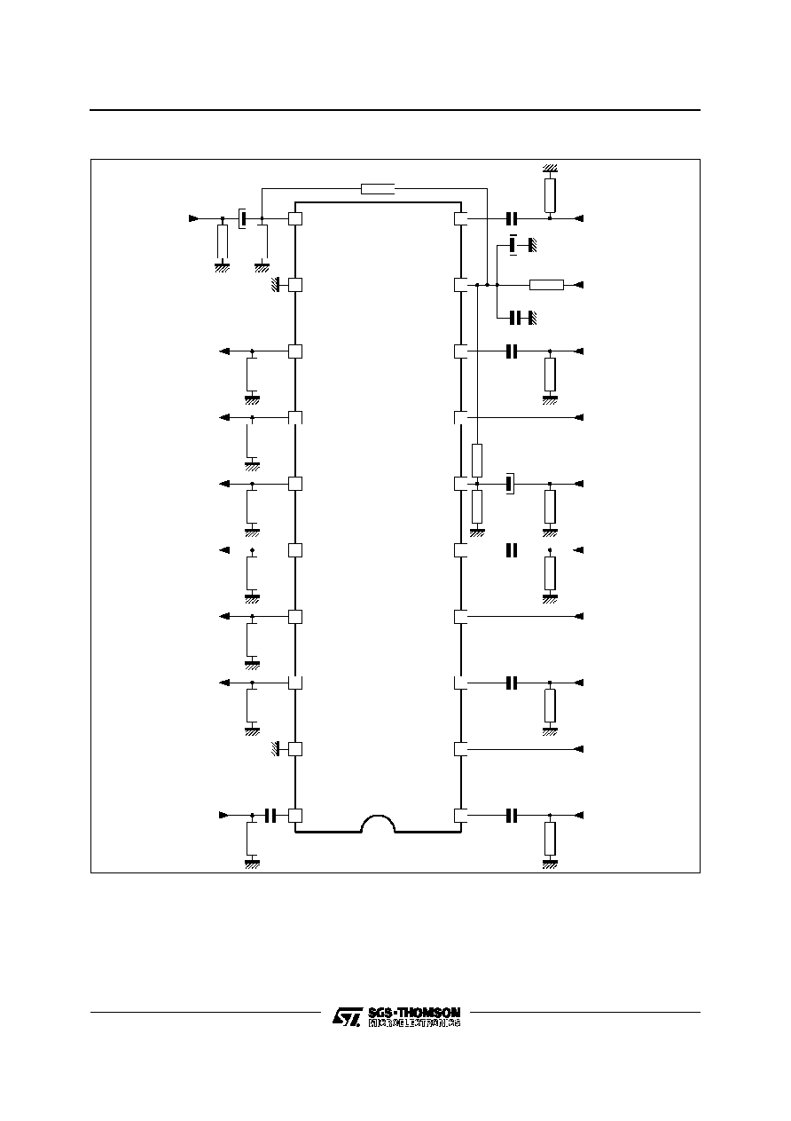
TYPICAL APPLICATION
1 - When any input is not used, it must be bypassed
to ground through a 220nF capacitor.
2 - An important improvement can be achieved
considering the input crosstalk by means of the
application (see technical note).
CROSSTALK IMPROVEMENT
TEA6415C
7/10

CVBS1
CVBS2
CVBS3
Ye xt
Yint
V
CC
V
CC
/2
Cint
Y + C
Yout1 Cout1
CVBSout1
Yout2
Cout2
CVBSout2
BUS
DECODER
Ce xt
V
CC
/2
Y, C
ADDER
Y, C
SEPARATOR
T
E
A
6
4
1
5
C
V
CC
6415C-09.EPS
OTHER APPLICATION DIAGRAM EXAMPLE
TEA6415C
8/10

PM-DIP20.EPS
PACKAGE MECHANICAL DATA
20 PINS � PLASTIC DIP
Dimensions
Millimeters
Inches
Min.
Typ.
Max.
Min.
Typ.
Max.
a1
0.254
0.010
B
1.39
1.65
0.055
0.065
b
0.45
0.018
b1
0.25
0.010
D
25.4
1.000
E
8.5
0.335
e
2.54
0.100
e3
22.86
0.900
F
7.1
0.280
I
3.93
0.155
L
3.3
0.130
Z
1.34
0.053
DIP20.TBL
TEA6415C
9/10

Information furnished is believed to be accurate and reliable. However, SGS-THOMSON Microelectronics assumes no responsibility
for the consequences of use of such information nor for any infringement of patents or other rights of third parties which may result
from its use. No licence is granted by implication or otherwise under any patent or patent rights of SGS-THOMSON Microelectronics.
Specifications mentioned in this publication are subject to change without notice. This publication supersedes and replaces all
information previously supplied. SGS-THOMSON Microelectronics products are not authorized for use as critical components in life
support devices or systems without express written approval of SGS-THOMSON Microelectronics.
�
1996 SGS-THOMSON Microelectronics - All Rights Reserved
Purchase of I
2
C Components of SGS-THOMSON Microelectronics, conveys a license under the Philips
I
2
C Patent. Rights to use these components in a I
2
C system, is granted provided that the system confo rms to
the I
2
C Standard Specifications as defined by Philips.
SGS-THOMSON Microelectronics GROUP OF COMPANIES
Australia - Brazil - China - France - Germany - Hong Kong - Italy - Japan - Korea - Malaysia - Malta - Morocco
The Netherlands - Singapore - Spain - Sweden - Switzerland - Taiwan - Thailand - United Kingdom - U.S.A.
PM-SO20.EPS
PACKAGE MECHANICAL DATA
20 PINS � PLASTIC MICROPACKAGE (SO)
Dimensions
Millimeters
Inches
Min.
Typ.
Max.
Min.
Typ.
Max.
A
2.65
0.104
a1
0.1
0.3
0.004
0.012
a2
2.45
0.096
b
0.35
0.49
0.014
0.019
b1
0.23
0.32
0.009
0.013
C
0.5
0.020
c1
45
o
(typ.)
D
12.6
13.0
0.496
0.512
E
10
10.65
0.394
0.419
e
1.27
0.050
e3
11.43
0.450
F
7.4
7.6
0.291
0.299
L
0.5
1.27
0.020
0.050
M
0.75
0.030
S
8
o
(Max.)
SO20.TBL
TEA6415C
10/10