 | –≠–ª–µ–∫—Ç—Ä–æ–Ω–Ω—ã–π –∫–æ–º–ø–æ–Ω–µ–Ω—Ç: TEA7063FP | –°–∫–∞—á–∞—Ç—å:  PDF PDF  ZIP ZIP |
TEA7063
SPEECH CIRCUIT WITH POWER MANAGEMENT
PRELIMINARY DATA
2/4 WIRES INTERFACE WITH
- double antisidetone network
- AC impedance externally programmable
- Rx output dynamic programmable
- AGC attack-disconnect points programmable
ANTI-CLIPPING/ANTI DISTORTION CIRCUIT
PROGRAMMABLE
DTMF INTERFACE
3.3 VOLTS SUPPLY FOR MICROPROCES-
SOR OR DIALER
EXTRA CURRENT SUPPLY PROGRAMMA-
BLE FOR LOUD SPEAKER
DC
CHARACTERISTIC
PROGRAMMABLE
FOR ALL SPECIFICATION
LOW CURRENT OPERATION
DESCRIPTION
The TEA7063 is designed to meet the different
worldwide specifications for telephone set in me-
dium and high range equipments.
This is advanced information on a new product now in development or undergoing evaluation. Details are subject to change without notice.
January 1994
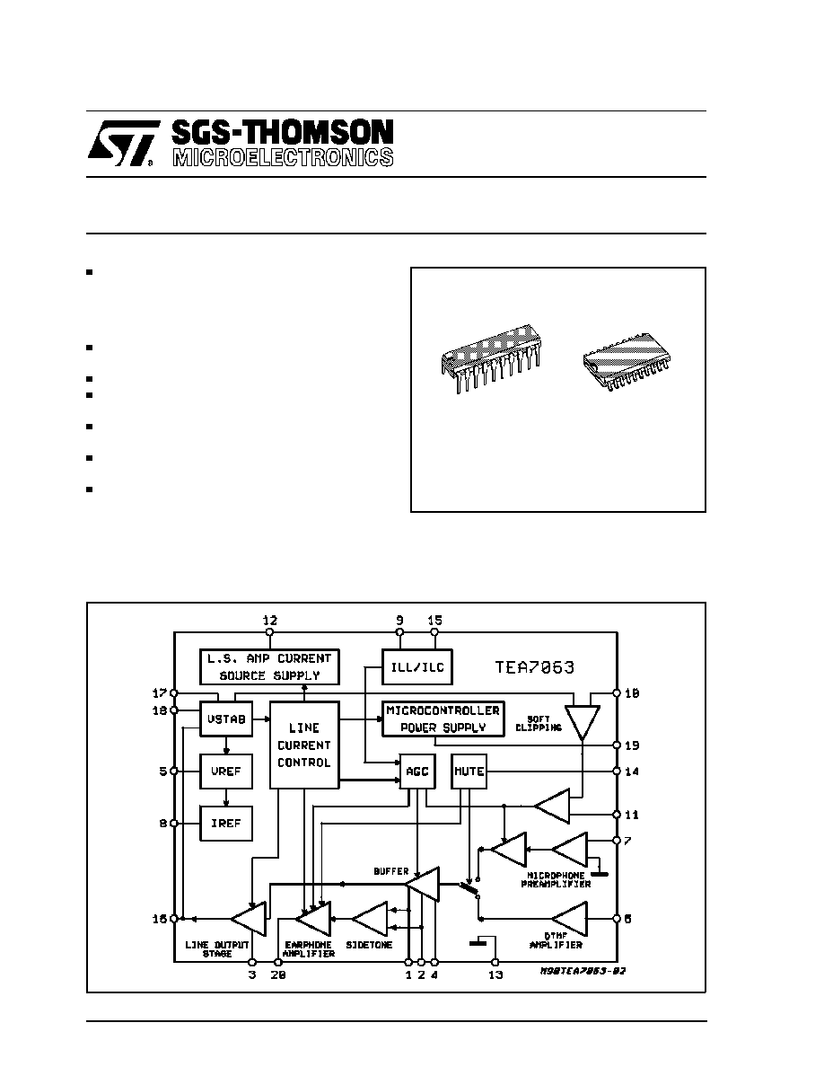
BLOCK DIAGRAM
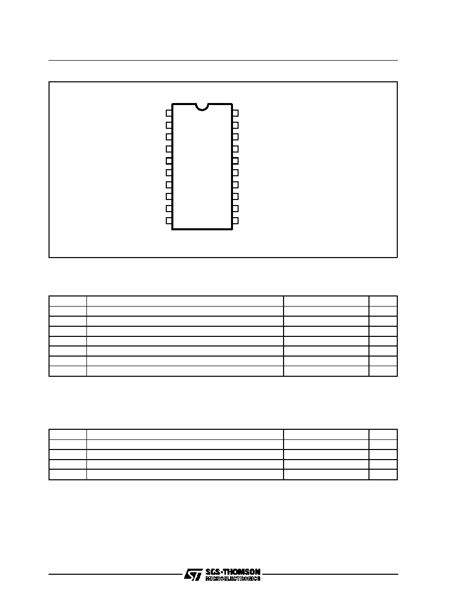
DIP20
SO20
ORDERING NUMBERS:
TEA7063FP
TEA7063DP
1/15
LONG LINE SIDETONE
SHORT LINE SIDETONE
IMPEDANCE
BUFFER OUTPUT
V-REF
MICROPHONE INPUT
DTMF INPUT
I-REF
I START
1
3
2
4
5
6
7
8
9
CURRENT SUPPLY FOR L.S. AMP
GND
MIC/MIC-EARPHONE MUTE
V-LINE
I SLOPE
V-CAPA
NOISE FILTER
MICROCONTROLLER POWER SUPPLY
EARPHONE
20
19
18
17
16
14
15
13
12
D93TL021
SQUEEZING THRESHOLD
10
SOFT-CLIPPING FILTER
11
PIN CONNECTION (Top view)
ABSOLUTE MAXIMUM RATINGS
Symbol
Parameter
Value
Unit
Max. Current DC (steady)
150
mA
Max. Voltage AC (steady)
7.5
V
Max. Voltage AC + DC (steady)
9
V
Max. Current (20ms) ONE SHOT
1
A
Max. Voltage (20ms) ONE SHOT current < 1A
12
V
P
tot
Total Power Dissipation
1
W
T
J
Junction Temperature
130
∞
C
MAXIMUM OPERATING CONDITION
Symbol
Parameter
Value
Unit
V
DC
DC Voltage
7
V
V
AC
AC Voltage
2.2
Vp
I
DC
DC Current
110
mA
T
OP
Temperature Range
-20 to 70
∞
C
TEA7063
2/15
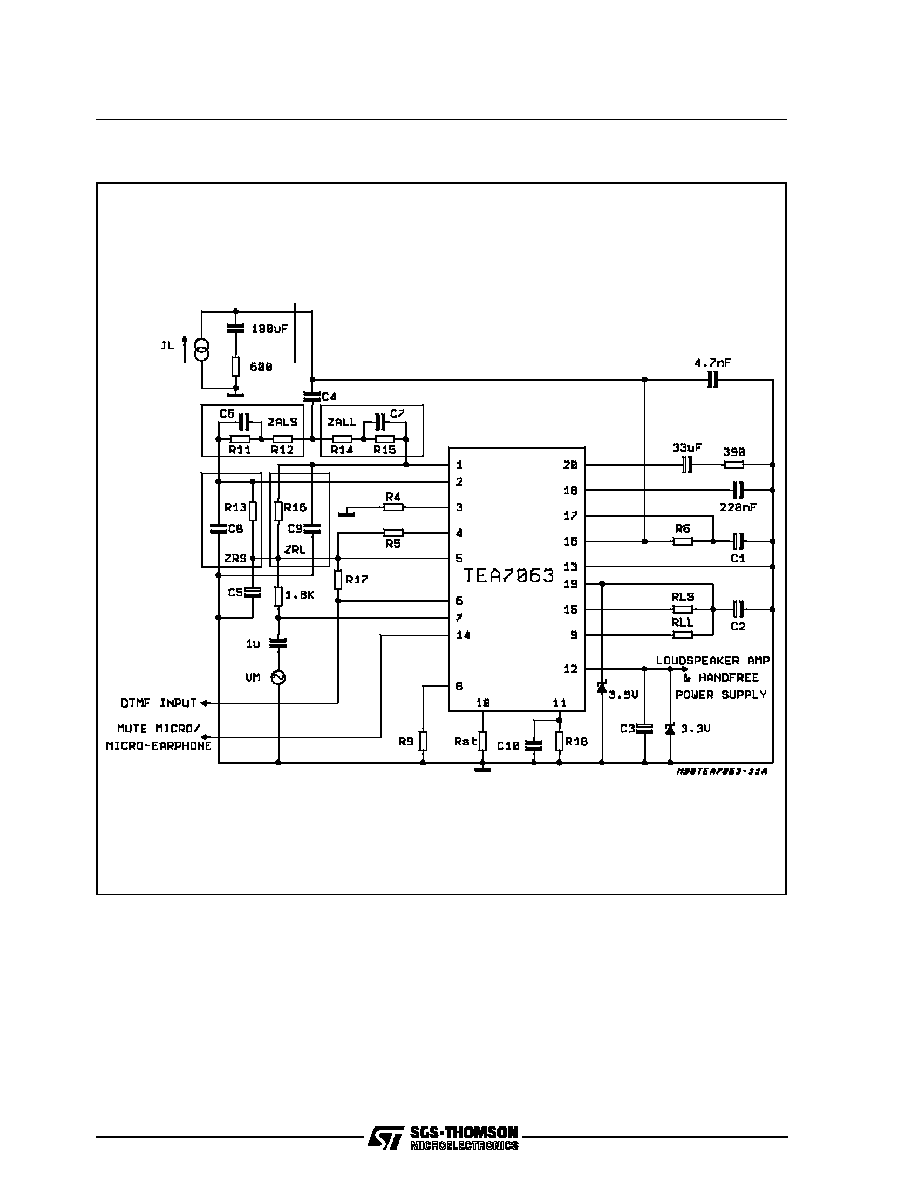
TEST CIRCUIT
R4 = 75
R5 = 5.1K
R6 = 22K
R9 = 100K
R11 = 140K
R12 = 0
R13 = 2.7K
R14 = 0
R15 = 140K
R16 = 2.7K
R17 = 1.8K
R18 = 560K
C1 = 47
µ
F
C2 = 4.7
µ
F
C3 = 47
µ
F
C4 = 470nF
C5 = 100
µ
F
C6 = 47pF
C7 = 47pF
C8 = 2.2nF
C9 = 2.2nF
C10 = 150nF
RLL = 150K
RLS = 100K
RST = 330K
TEA7063
3/15
ELECTRICAL CHARACTERISTICS (T
amb
= 25
∞
C; f = 1KHz; R9 = 100K
; unless otherwise specified)
Symbol
Parameter
Test Condition
Min.
Typ.
Max.
Unit
V
C
Stabilized Voltage (pin 17)
I
L
= 25mA; R9 = 100K
2.25
2.5
2.75
V
Iint
Internal Bias Current (pin 17)
I
L
= 25mA
I
L
= 25mA; R9 = 180K
(V16 - R6*Iint +V
C
)
120
140
105
160
µ
A
µ
A
V
ref
Reference Voltage
I
L
= 25mA
1.05
1.2
1.35
V
I
ref
Current at V
ref
-100
+10
µ
A
V
mp
Stabilized Supply at pin 19
3.1
3.3
3.5
V
I
cmp
Charging Current at Pin 19
Pin 17 = GND
0.6 X
I
line
mA
I
spm
Static Current at Pin 19
I
L
= 25mA; R9 = 100K
1.1
1.5
mA
I
L
= 25mA; R9 = 180K
0.85
mA
I
imp
Internal Consumption
80
110
150
µ
A
I
ea
Supply Current for Parallel
Circuits (pin 12)
I
L
= 25mA
I
L
= 75mA
10
50
12
57
mA
mA
V
mh
V
mb
Mute Microphone (pin 14)
ON
OFF
1.6
0.25
0.8
V
V
V
mh
V
mb
Mute Earphone (pin 14)
ON
OFF
2.7
0.25
2.1
V
V
I
mleak
Mute Leakage Current (pin 14)
V
14
= 5V
20
µ
A
G
S
AGC
S
Tx Gain Long Line
I
L
= 25mA
41.5
-7
42.5
-6
43.5
-5
dB
dB
G
m
f
DTMF Gain
Pin 14 > 1.6V
41.5
42.5
43.5
dB
THD
S
Tx Distortion
I
L
= 25mA
V
mic
= -3dBm -GS
V
mic
= -3dBm -GS + 15dB
3
10
%
%
Z
e
Microphone Impedance
20
K
N
Tx
Tx Noise (psometric)
I
L
= 25mA
2K
at Pins 5-7
-74
dBm
psoph
R
S
Tx Attenuation in Mute Mode
I
L
= 25mA
Pin 14 > 1.6V
60
dB
G
r
AGC
r
Rx Gain Long Line
Line Lenght
I
L
= 25mA
29
-7
30
-6
31
-5
dB
dB
THD
r
Rx Distortion
I
L
= 25mA
Vro = 500mV
Vro = 630mV
3
10
%
%
N
Rx
Rx Noise
I
L
= 25mA
-74
dBmp
R
r
Rx Attenuation in Mute Mode
I
L
= 25mA
Pin = 14 > 2.7V
50
dB
G
as
Antisidetone
I
L
= 25mA
22
dB
Z
ac
AC Impedance
I
L
= 25mA
500
650
800
G
rs
Confidence Level = V
LI NE
/V
REC
(in DTMF)
Pin 14 > 2.7V
35.5
38.5
41.5
dB
I
ST
Soft Clipping Current Level
Control (pin 10)
I
L
= 25mA; R9 = 100K
I
L
= 25mA; R9 = 180K
2.30
2.55
1.4
2.80
mA
µ
A
V
ST
Control Voltage Range (Pin 10)
V
ST
= R
ST x
I
ST
0
1
V
TEA7063
4/15
CIRCUIT DESCRIPTION
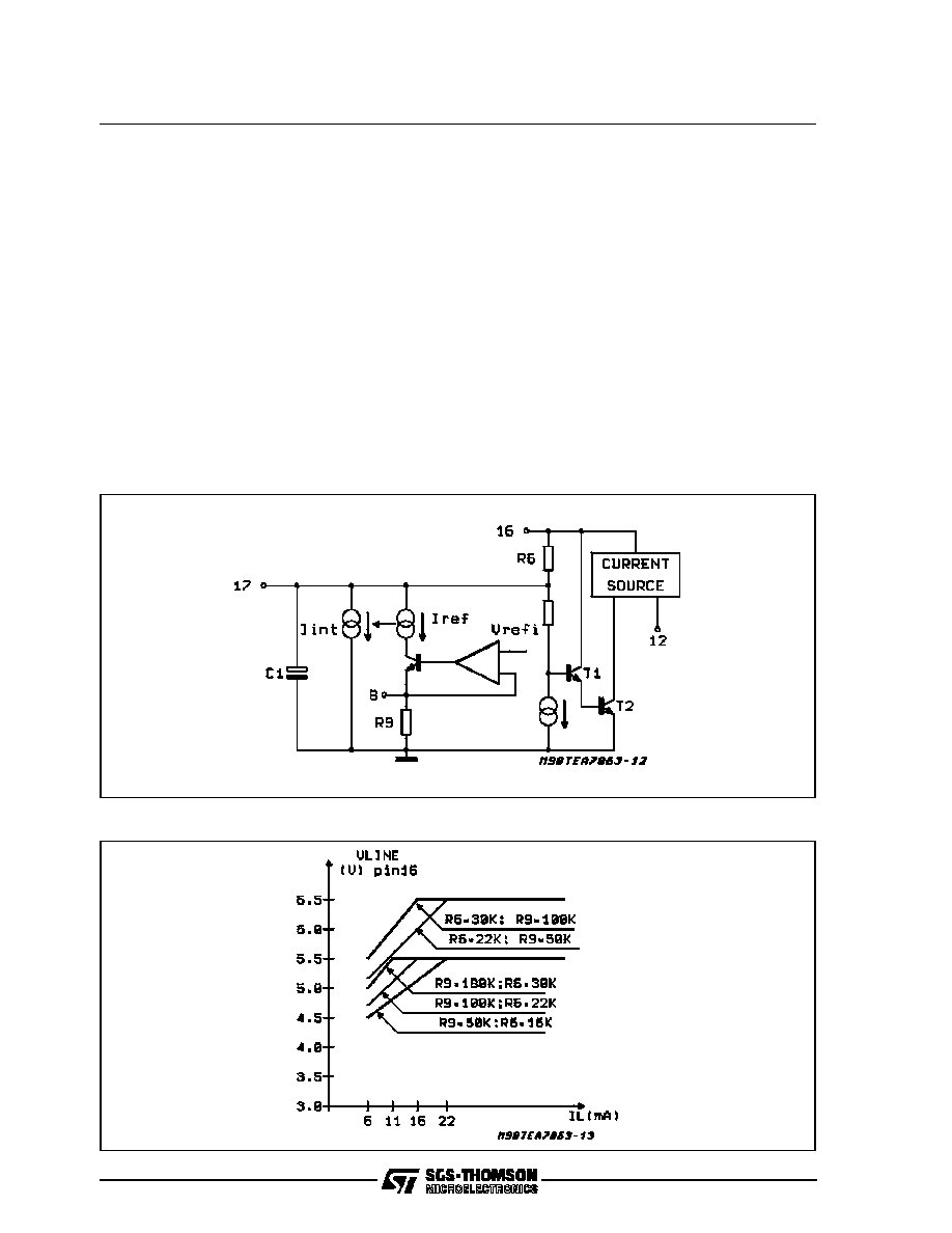
1. DC CHARACTERISTICS
1.1 V
C
(pin 17)
The stabilized voltage VC is connected to Vline
(pin 16) through an internal shunt regulator T1,
T2, which presents to the line a high AC imped-
ance at frequecncies higher than 200Hz. At this
purpose the value of C1 (at pin 17) must be not
lower than 47
µ
F (suggested value is 100
µ
F).
The shunt regulator, T1 and T2, also controls the
extra current source, or power management, at
pin 12 (see also paragraph 6).
1.2 V
LINE
(pin 16)
The line voltage (pin 16) is determined by the
value of the external resistor R6 and by the inter-
nal current, I
int
, flowing between V
C
(pin 17) and
Ground (see also paragr.: 1.1):
V
LINE
= V
C
+ R 6 x I
int
V
C
is fixed by design at about 2.5V.
I
int
is reversely related to R9:
I
int
= 8 Volt/R9 + 60
µ
A at I
L
> 25mA
I
int
= 4 Volt/R9 + 60
µ
A at I
L
= 6mA
where I
L
depends on I
LB
(see supply manage-
ment)
V
LINE
must be externally adjusted (with R6) to
guarantee both DC and AC characteristic in ac-
cordance to the specific standard of the different
adminastrations.
Another adjustment of the DC characteristic is
possible with R9. Increasing the value of R9
causes a decrease of I
int
and consequently a re-
duction of the product I
int
x R9. (see also Para-
graph 7)
Figure 2
Figure 1
TEA7063
5/15

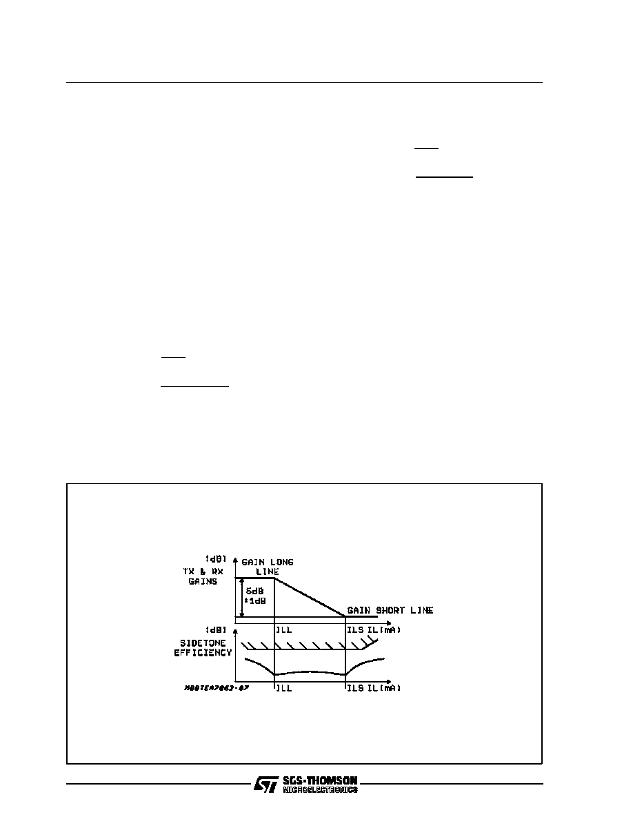
2. TRANSMISSION CHAIN
2.1 A.G.C. In Transmission
The transmission gain between Microphone Input
(pin 7) and Vline (pin 16) is internally decreased
of 6dB when the line current varies from ILL to
ILS with a constant AC load of 600
.
The values of ILL (long line current) and ILS (short
line current) are programmable through I-start (pin
9) and I-slope (pin 15) (see also paragr. 4).
2.2 Sending Impedance
The impedance of the Output Stage Amplifier, Z
out
,
is determined by the impedance Z4 (at pin 3).
Z
out
= 10.65 xZ4
The total AC impedance shown to the line is the
parallel
Z
par
= Z
out
//Z
int
//Z
ext
where:
- Z
int
= 10K
//8.5 nF (internal)
- Z
ext
= R6//C4 (at pin 16)
2.3 Sending Mute
In normal speech operation (V
mute
at pin 14 <
0.8V), the signal at Microphone Input (pin 7) is
amplified to V
line
(pin 16) with the gain Gs (long
line) or 6dB lower (shorter lines) depending on
AGC control (see paragr. 4).
In sending mute condition (V 14 > 1.6V) these
gains are reduced of at least 60dB. In the same
condition, DTMF input (pin 6) is activated, with
gain Gmf to the line independent from I
line
lenght.
2.4 Antisidetone Buffer
The signal coming from the sending preamplifier
is internally presented at pin 4 and than buffered
to pins 1 and 2 for sidetone cancellation (see
paragraph 3.2).
Figure 3
TEA7063
6/15
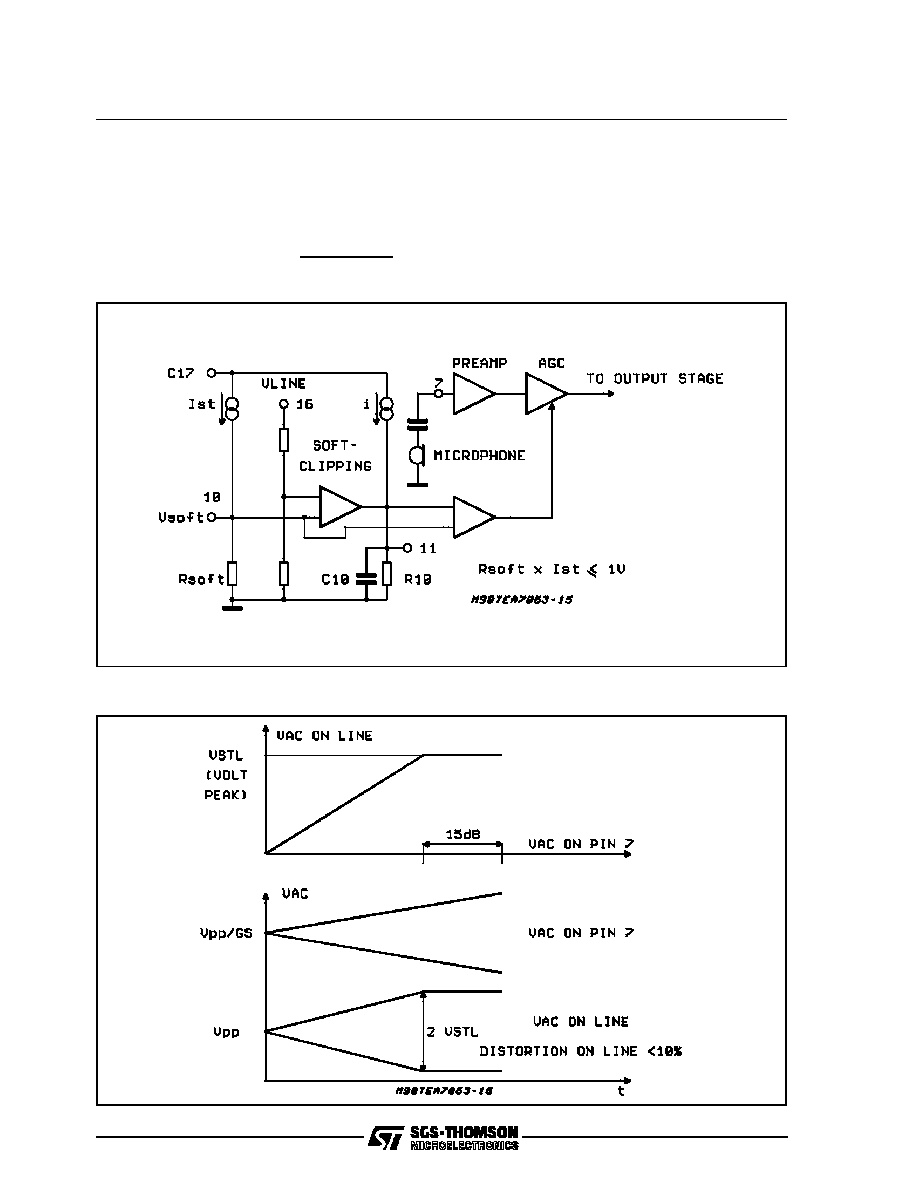
2.5 Soft Clipping
To avoid distortion on line, the TEA7063 has a
"soft clipping" on transmit channel.
The resistor (Rsoft) on pin 10 fixes the maximum
AC peak dynamic on the line: V
STL
V
STL
(Vp) = Vpin16(DC) -1.44
∑
R
soft
(
pin 10
)
R9
(
pin
8
)
where Rsoft
1V
I
ST
I
ST
=
470mV
2
R9
(
pin
8
)
The capacitor (C10) and the resistor (R10) con-
nected on pin 11 fixe the constant time of the soft
clipping.
Recommended values: C10 = 150nF;
R10 = 560K
Figure 4
Figure 5: Transmit Curves
TEA7063
7/15
3. RECEIVE CHAIN
3.1 A.G.C. In Receive
As described for the transmission chain, also the
receiving gains Gr, from pins 1 and 2 to pin 20,
have a reduction of 6dB when Iline moves from
ILL to ILS (see also paragr. 4).
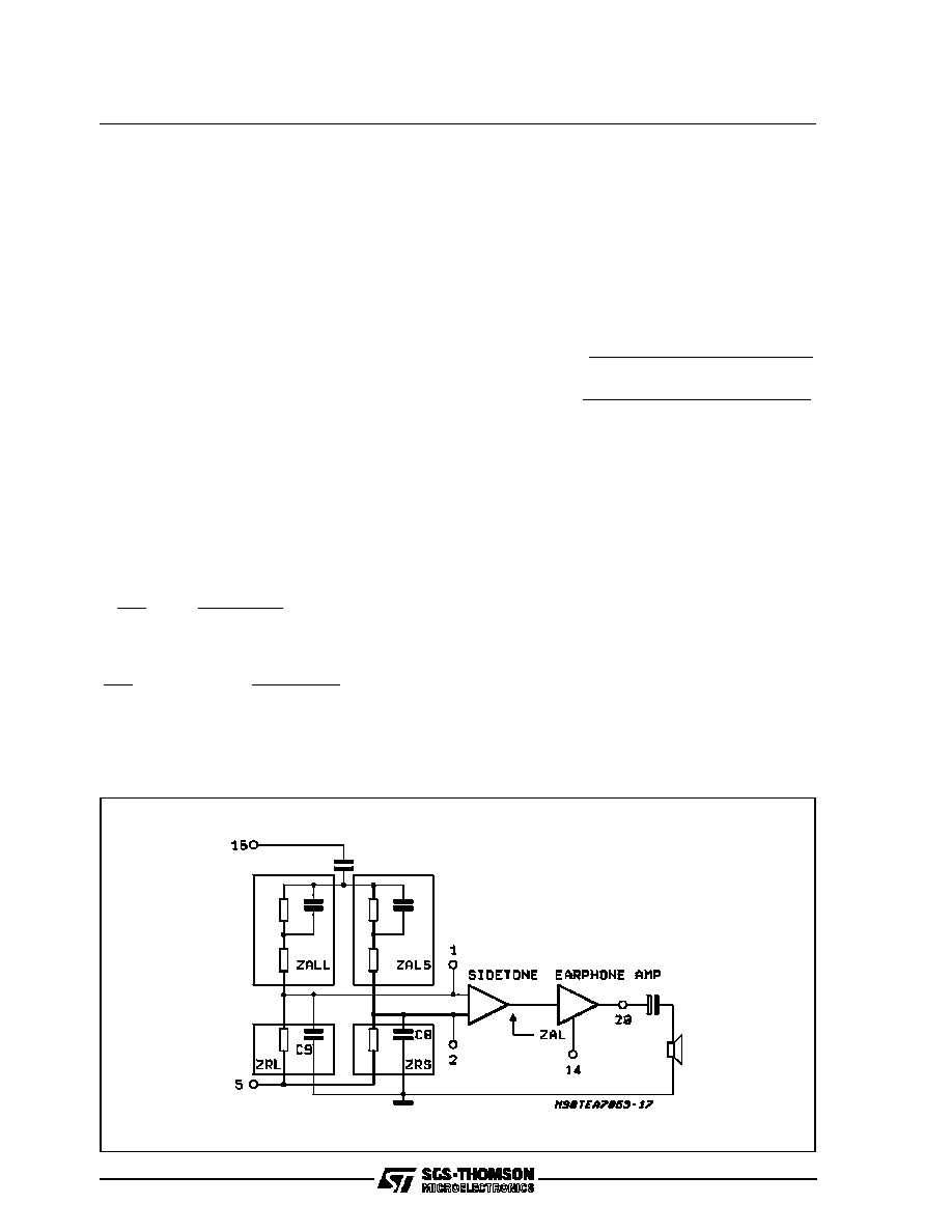
3.2 Sidetone Compensation
The circuit is provided with a double anti-sidetone
network to optimize both at long and short lines.
In case double antisidetone network is not re-
quested by the application needs, pins 1 and 2
can be connected to each other and 5 external
passive components can be saved (ZALL and
ZRL).
Before entering pins 1 and 2, the received signal
is areduced by the two attenating networks:
- ZALL/ZRL to pin 1 for long lines sidetone com-
pensation,
- ZALS/ZRS to pin 2 for short lines sidetone com-
pensation.
ZRL and ZRS define the total receive gains:
a)
V20
V16
=
G
r
∑
ZRL
ZRL
+
ZALL
for
long
lines
b)
V20
V16
= (
G
r
-
6dB
) ∑
ZRS
ZRS
+
ZALS
for short lines
ZALL and ZALS define the sidetone compensa-
tion of the circuit.
The equivalent balancing impedance is given by
the formula:
ZAL = K
∑
ZALS + (1 - K)
∑
ZALL
where:
-K = 0 at I
LINE
= ILL or lower (long line)
-K varies linearly from 0 to 1 with Iline between
ILL and ILS
-K = 1 at I
LINE
= ILS or higher (short line)..
Calculations to define ZALL and ZALS are:
a)
ZALL = 70
∑
R5
∑
Z
line
(
long
) / /
Z
ext
/ /
Z
int
/ /
Z
out
Z
out
b)
ZALL = 70
∑
R5
∑
Z
line
(
short
) / /
Z
ext
/ /
Z
int
/ /
Z
out
Z
out
where:
- Z
ext
= R6//C4//(Zelectret) (at pin 13)
- Z
int
= 10K
//8.5nF (internal impedance)
- Z
out
= 10.65
∑
Z4 (at pin 3; see paragr. 2.2)
- Zline (short) and (long) are the impedances of
the line at minimum and naximum line lenght
- R5 = 5.1K
±
1% (typically)
3.3 AC Impedance
The total AC impedance of the circuit to the line
is:
ZAC = Zout//Zint//Zext (ZALS, ZALL >>ZAC)
3.4 Receive Mute (and confidence level)
When the receive channel is muted (Vpin 14 >
2.7V) the receive gain is reduced of 60dB minimum.
Figure 6
TEA7063
8/15
In this condition an internal connection is acti-
vated from line DTMF output (pin 16) to Receive
Output (pin 20) with an attenuation GRS = 38.5dB
to provide acoustic feedback of the DTMF emis-
sion.
4. A.G.C AND SIDETONE PROGRAMMING
4.1 Programmable Controls
AGC and sidetone attack and disonnect points (or
currents) are programmable externally through
two independents pins, I-start (pin 9) and I-slope
(pin 15).
4.2 I-Start (pin 9)
An external resistor RLL connected between I-
start (pin 9) and Microprocessor Supply (pin 19)
controls the attack point of AGC and ZAL (an-
tisidetone Z).
ILL is the line current at which the control starts.
Formulas for ILL and RLL with R9 = 100K are:
ILL =
2880
RLL
+
11mA
RLL =
2880
(
ILL
-
11mA
)
4.3 I-Slope (pin 15)
An external resistor RLS connected between
I-slope (pin 15) and Microprocessor Supply (pin
19) controls the disconnected point of AGC and
ZAS (antisidetone Z). ILS is the line current at
which the control stops. Formulas for ILS and
RLS with R9 = 100K are:
ILS =
4680
RLS
+
ILL;
RLS =
4680
(
ILS
-
ILL
)
4.4 A.G.C. OFF (pin 9 and 15)
Programming ILL and ILS respectively higher
than 70mA and 450mA is forcing the IC in AGC
OFF Condition.
Suggested external components are:
RLL = 51K
and RLS = 10K
In this case sending, receiving gain and sidetone
compensation are independent of the line lenght.
Pins 1 and 2 can be connected to each other sav-
ing 5 passive external components at pin 2.
4.5 Secret Function for Private (pin 14)
The two separate thresholds for sending and Re-
ceiving Mute (pin 14) allow "Secret Function"
(only microphone muted).
Pin 14 can be set:
a) between 0.25V and 0.8V for speech mode,
b) between 1.6V and 2.1V for "secret" mode (mi-
crophone muted),
c) between 2.7V and 3.3V for "all muted" mode
Figure 7
TEA7063
9/15
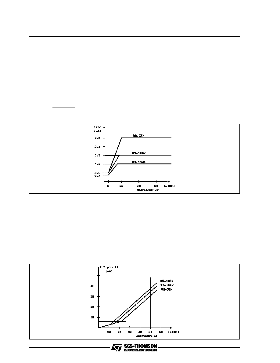
6. CURRENT SOURCE FOR SPEAKERPHONE
6.1 Current Source (pin 12)
Most of the DC current available from the line is
delivered by the speech circuit at the output I
source
(pin 12) through an internal current generator.
Typical values of this current, l
LS
with R9 = 100K,
are:
I
LS
= (0.3
∑
I
LINE
)
for I
LINE
< 16.5mA
I
LS
= (0.9
∑
I
LINE
-10mA) for I
LINE
> 16.5mA
(ex: I
LINE
= 16mA then I
LS
= 5mA
I
LINE
= 30mA then I
LS
= 17mA
I
LINE
= 60mA then I
LS
= 44mA).
The voltage level at pin 12 must be defined by an
external regulator (i.e.: zener) and, if necessary,
filtered with a capacitor (47 to 220
µ
F).
In case V
LINE
(at pin 16) approaches voltage at
pin 12, then the internal current source switches
off and its DC current is shunt to ground through
and internal
complementary generator, thus
avoiding any negative effect on the AC and DC
impedances of the telephone set application.
5. MICROPROCESSOR INTERFACE
5.1 Microprocessor Supply (pin 19)
At "off-hook" the first priority of the circuit is to
make some current available at the Microproces-
sor Supply (pin 19) to charge quickly the external
capacitor C2.
This charging current is I
cpm
= 0.6
∑
I
LINE
T-charge of about 10ms is necessary, with C2 =
47/
µ
F. to charge pin 19 at the specified value of
3.3V typical at I
LINE
= 25mA:
T-charge =
3.3V
∑
C2
0.6
∑
I
LINE
typically
V
mp
= 3.3V in normal operation and current in-
creases linearly from 0.5mA min, at I
LINE
= 6mA,
to1.5mA, at I
LINE
= 25mA, remaining stable for
higher values of I
LINE
. (with R9 = 100K)
In general:
I
mp
=
130Volt
R9
+ 0.3mA at I
L
> 25mA
I
mp
=
11Volt
R9
+ 0.3mA at I
L
> 6mA
A zener of 3.9V typical is generally suggested to
Figure 8
Figure 9
TEA7063
10/15
7. INTERNAL DESCRIPTION OF CURRENT
MANAGEMENT
7.1 Internal Power Supply Management
R9 fixes the line power supply management.
R9 fixes the values of: I
ear
, I
up
, I
ref
and ILS.
A current line information is used to modifie the
values of I
ear
, I
up
, I
ref
and ILS between a minimum
and a maximum values.
On Fig 10:
The transmit output stage is represented by a cur-
rent source (I
tr
). The I
tr
value depends of the DC
voltage on V
LINE
(pin 16) and R
ZAC
value.
The other internal stages connected to V
LINE
(pin
16) are represented by a constant 1.3mA current
source.
7.2 DC Characteristics (internal)
The DC characteristic is equals to:
V
LINE
(pin 16) = V
C
(pin 17) + R6
∑
I
int
Iint is the sum of all the current sources con-
nected on VC (pin 17):
[I
p
+ I
ref
+ Vpin17 / (r7 + r8)]
- I
p
is the bias internal operational amplifiers
power supply.
- I
ref
= 1 / 3
∑
(V
refi
/ R9); with V
refi
= 470mV
- I
ref
= 156 / R9 mA
The current line information changes Iint value;
at low line current (6mA): I
int
= 4V / R9 + 60
µ
A
at low line current (IL = ILb): I
int
=8V / R9 + 60
µ
A
7.3 Microcontroller Supply (internal)
I
up
= [(p2 / r2)
∑
I
ref
+ 0.3] mA = [(p2 / r2)
∑
156 /
R9) + 0.3] mA
The current line information changes p2/r2 value;
at low line current (6mA): p2 / r2 = 70
at a line current (IL = ILb): p2 / r2 = 820
7.4 Earphone Current Supply (internal)
I
ear
= (p1 / r1)
∑
I
ref
mA = (p1 / r1)
∑
(156 / R9) mA
The current line information changes p1/r1 value;
at low line current (6mA): (p1 / r1) = 200
at a line current (IL = ILb): p1 / r1 = 2700
The maximum peak dynamic on the earphone is:
V
pear
= Z
ear
∑
I
ear
7.5 Transmit Output Stage (internal)
The output stage bias current depends of the DC
voltage on pin 16 and on R
ZAC
impedance.
I
tr
=
0.1425
∑
V
LINE
-
0.517
R
Z
(R
Z
is the resistor
connected betwee pin3 and the ground)
7.6 Loudspeaker Current Source (internal)
The current source for external peripherals has
two slopes:
- First slope; before I
ear
, I
up
, I
tr
and I
int
are stabi-
lized at their maximum values: (IL = ILb)
ILS = 0.285
∑
IL
- Second slope; after I
ear
, I
up
, I
tr
and I
int
are sta-
bilized at their maximum values: (for IL > ILb)
(ILS) = 0.91
∑
(I
LINE
I
ear
, I
up
, I
tr
and I
int
are stabilized at their maximum
values between 16 and 26mA, the absolute IL
value depends of R9 value. The line current (ILb)
where I
ear
, I
up
,
Itr
, I
int
are stabilized at their maxi-
mum values and where the slope of ILS change
is:
ILb =
I
ear
+
I
up
+
I
tr
+
I
int
+
1.3
0.715
7.7 Numerical Example
1) R9 = 100K
; R6 = 25K
DC characteristic = 6V for I
int
max:
= 5V for I
int
min:
I
int
min (IL = 6mA) = 4 /100K + 60 = 100
µ
A
I
int
min (IL = ILb) = 8 /100K + 60 = 140
µ
A
Vpin17 = 2.5V
R6 = 25K
Vpin16 min (IL = 6mA) = 2.5 + 25
∑
100E - 3 = 5V
Vpin16 max (IL = ILb) = 2.5 + 25
∑
140E - 3 = 6V
Current Sources
I
up
min (IL = 6mA) = 0.4mA
I
up
max (IL = ILb) = 1.6mA
I
ear
min (IL = 6mA) = 0.3mA
I
ear
max (IL = ILb) = 4.2mA
with R
Z
= 75
I
tr
min (IL = 6mA) = 2.6mA
I
tr
max (IL = ILb) = 4.5mA
ILS min (IL = 6mA) = 1.3mA
ILb
ILb =
1.6
+
4.2
+
4.5
+
0.14
+
1.3
0.715
mA
ILb = 16.5mA
ILS (for IL = ILb) = 0.285
∑
ILb = 4.7mA
at IL = 100mA:
(ILS) = 0.91
∑
(IL) = 0.91
∑
(100 - 16.5) = 76mA
ILS = 4.7 + 76 = 80.7mA
2) R9 = 56K
; R6 = 18K
DC characteristic = 6.1V for I
int
max:
= 4.8V for I
int
min:
TEA7063
11/15

I
int
min (IL = 6mA) = 4 /56K + 60 = 130
µ
A
I
int
min (IL = ILb) = 8 /56K + 60 = 200
µ
A
Vpin17 = 2.5V
R6 = 18K
Vpin16 min (IL = 6mA) = 2.5 + 18
∑
130E - 3 = 4.85V
Vpin16 max (IL = ILb) = 2.5 + 18
∑
200E - 3 = 6.1V
Current Sources
I
up
min (IL = 6mA) = 0.5mA
I
up
max (IL = ILb) = 2.5mA
I
ear
min (IL = 6mA) = 0.55mA
I
ear
max (IL = ILb) = 7.5mA
with R
Z
= 75
I
tr
min (IL = 6mA) = 2.35mA
I
tr
max (IL = ILb) = 4.5mA
ILS min (IL = 6mA) = 1.17mA
ILb
ILb =
2.5
+
7.5
+
4.5
+
0.2
+
1.3
0.715
mA
ILb = 22.4mA
ILS (for IL = ILb) = 0.285
∑
ILb = 6.4mA
at IL = 100mA:
(ILS) = 0.91
∑
(IL) = 0.91
∑
(100 - 22.6) = 64mA
ILS = 6.4 + 64 = 70.4mA
Figure 10: Line Power Supply Management
TEA7063
12/15
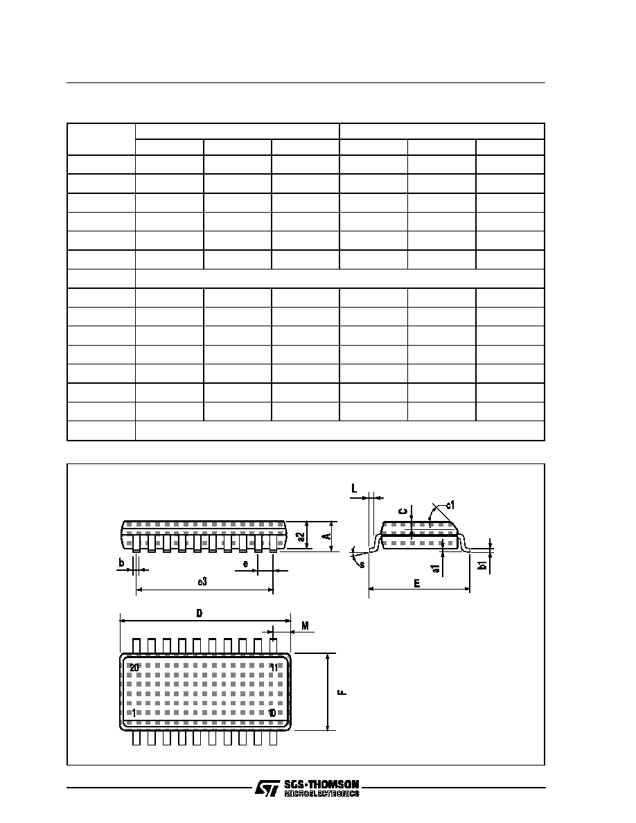
SO20 PACKAGE MECHANICAL DATA
DIM.
mm
inch
Min.
Typ.
Max.
Min.
Typ.
Max.
A
2.65
0.104
a1
0.1
0.2
0.004
0.008
a2
2.45
0.096
b
0.35
0.49
0.014
0.019
b1
0.23
0.32
0.009
0.013
C
0.5
0.020
c1
45
o
(typ.)
D
12.6
13.0
0.496
0.510
E
10
10.65
0.394
0.419
e
1.27
0.050
e3
11.43
0.450
F
7.4
7.6
0.291
0.300
L
0.5
1.27
0.020
0.050
M
0.75
0.030
S
8
o
(max.)
TEA7063
13/15
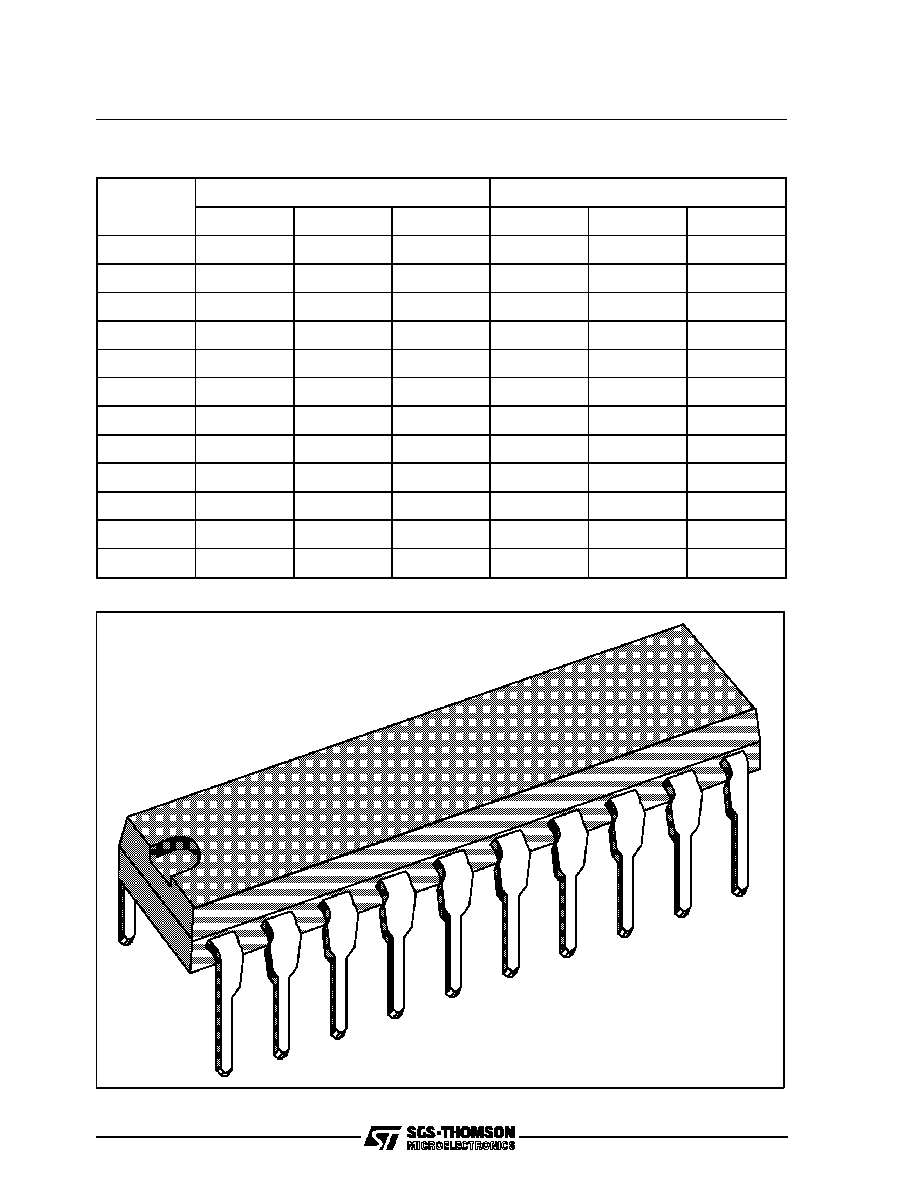
DIP20 PACKAGE MECHANICAL DATA
DIM
mm
inch
Min.
Typ.
Max.
Min.
Typ.
Max.
a1
0.254
0.010
B
1.39
1.65
0.055
0.065
b
0.45
0.018
b1
0.25
0.010
D
25.4
1.000
E
8.5
0.335
e
2.54
0.100
e3
22.86
0.900
F
7.1
0.280
i
3.93
0.155
L
3.3
0.130
Z
1.34
0.053
TEA7063
14/15

Information furnished is believed to be accurate and reliable. However, SGS-THOMSON Microelectronics assumes no responsibility for the
consequences of use of such information nor for any infringement of patents or other rights of third parties which may result from its use. No
license is granted by implication or otherwise under any patent or patent rights of SGS-THOMSON Microelectronics. Specifications men-
tioned in this publication are subject to change without notice. This publication supersedes and replaces all information previously supplied.
SGS-THOMSON Microelectronics products are not authorized for use as critical components in life support devices or systems without ex-
press written approval of SGS-THOMSON Microelectronics.
©
1994 SGS-THOMSON Microelectronics - All Rights Reserved
SGS-THOMSON Microelectronics GROUP OF COMPANIES
Australia - Brazil - France - Germany - Hong Kong - Italy - Japan - Korea - Malaysia - Malta - Morocco - The Netherlands
Singapore - Spain - Sweden - Switzerland - Taiwan - Thaliand - United Kingdom - U.S.A.
TEA7063
15/15