 | ÐлекÑÑоннÑй компоненÑ: TEA7532 | СкаÑаÑÑ:  PDF PDF  ZIP ZIP |
Äîêóìåíòàöèÿ è îïèñàíèÿ www.docs.chipfind.ru
TEA7532
July 1993
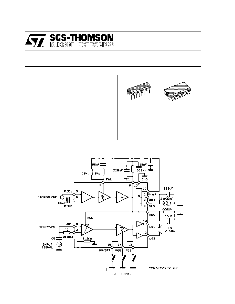
MONITOR AMPLIFIER
.
PROGRAMMABLE GAIN IN STEPS OF 6 dB
.
ON/OFF POSITION
.
LOW VOLTAGE
.
POWER : 100 mW AT 5 V
DESCRIPTION
This 16 pins IC is designed for monitor
(loudspeaker) telephone set and provides :
a) Signal amplification for monitoring (loudspeaker)
b) Antiacoustic feedback (antilarsen)
c) Antidistortion by automatic gain adaptation
d) Antilarsen adjustment (full duplex)
DI P16
SO16
ORDERING NUMBERS : TEA7532DP (DIP16)
TEA7532FP (SO16)
BLOCK DIAGRAM
1/16
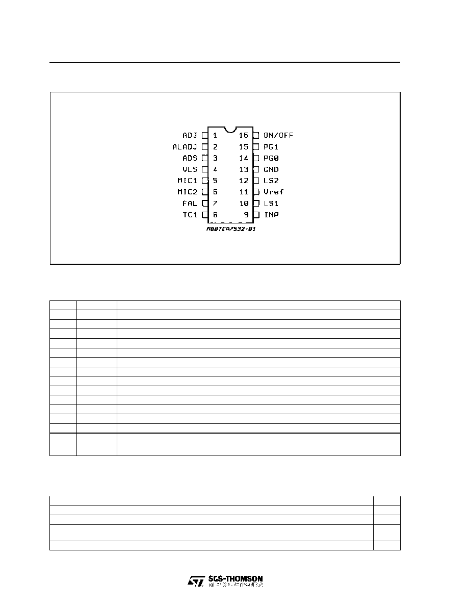
PIN DESCRIPTION
N
°
Symbol
Description
1
ADJ
Adjust Internal Reference V
LS
2
ALADJ
Antilarsen Adjustement
3
ADS
Antidistortion
4
V
LS
Supply
5
MIC1
Microphone Input
6
MIC2
Microphone input
7
FAL
Antilarsen Filter
8
TC1
Antilarsen Time Constant
9
INP
Input Signal
10
LS1
Output Loudspeaker 1
11
V
REF
Internal Resistance
12
LS2
Output Loudspeaker 2
13
GND
Ground
14
15
16
PG0
PG1
ON/OFF
Inputs Program Level to Loudspeaker
PIN CONNECTION (Top view)
ABSOLUTE MAXIMUM RATINGS
Symbol
Parameter
Value
Unit
T
op
Temperature Range
5 to + 45
°
C
V
LS
Supply Voltage
6
V
I
LS
Supply Current
for T > 300ms
for T
300ms
90
150
mA
mA
V
L
Voltage Level (pins, PG0, PG1, on/off)
0.6 > to V
S
+ 0.6
V
TEA7532
2/16
FUNCTIONAL DESCRIPTION
TEA7532 performs the following functions :
The circuit amplifies the incoming signal and feeds
it to the loudspeaker. PG0 and PG1 inputs are used
to set the loudspeaker gain in a range of 32dB to
14dB in 6dB steps.
The TEA7532 inputs (PG0, PG1, ON/OFF) permit
the loudspeaker to be cut-off thus ensuring privacy
of communication.
- The antilarsen (antiacoustic feedback) system is
incorporated.
- The maximum power available on a 50
imped-
ance loudspeaker is 25mW at 3 volts and 100mW
at 5V.
Limit values for external components :
R3 min = 5 k
(R3 adjust VLS), R7 max = 390 k
,
R6 min = R7/35
R max between pin 5 and 6 = 10k
+ C min = 10nF.
ELECTRICAL CHARACTERISTICS (T
amb
= 25
o
C, I
LS
= 30mA unless otherwise specified)
Symbol
Parameter
Test Conditions
Min.
Typ. Max.
Unit
V
LS1
V
LS
Supply
I
LS
= 2mA (fig. 7)
I
LS
= 30mA (fig. 7)
2.6
3.0
3.15
3.4
3.4
V
V
V
LSM
V
LS
Maximum
I
pin 1
= 50
µ
A (fig. 7 ; So = closed)
5.5
V
V
ADJ
Voltage Pin 1
I
LS
= 2mA to 30mA (fig. 7)
1.1
1.25
1.4
V
G
Loudspeaker Amplifier Gain =
V
10
-
V
12
V
9
ON/OFF
PG0
PG1
G000
G001
G010
G011
G100
GND
GND
GND
GND
V
LS
GND
GND
V
LS
V
LS
X
GND
V
LS
GND
V
LS
X
12
18
24
30
14
20
26
32
30
16
22
28
34
20
dB
dB
dB
dB
dB
THD
Distortion
f = 300Hz to 2kHz,
V
10
V
12
= 0.8V
RMS
,
G = G011, (fig. 8)
2
%
G2
[V(10) V(12)]/V2
P
G0
= P
G1
= V
LS
, V
8
= 0.8V (fig. 8)
30
32
34
dB
Z
MICIN
Microphone Input
Symetrical at (pins 5-6)
Asymetrical at (pin 6) fig. 9
4.5
k
Z
INPIN
Earphone Input
(fig. 9)
2.2
2.8
3.4
k
Z
IN2
Antilarsen Adjustment Input
1
1.2
1.45
k
V
OFFS
Ouput Offset
[V
(10)
V
(12)
]
G011 ; (fig. 8)
50
50
mV
I
ON/OFF
I
PG0
I
PG1
Input Current ON State
V
PG1
= 0V ; (fig. 8)
10
10
10
5
5
5
µ
A
µ
A
µ
A
I
ON/OFF
I
PG0
I
PG1
Input Current OFF State
V
PG1
= V
LS
; (fig. 8)
1
1
1
µ
A
µ
A
µ
A
V
IL ON/OFF
V
IL PG0
V
IL PG1
Input Voltage ON State
0.45
0.45
0.45
V
V
V
V
IH ON/OFF
V
IH PG0
V
IH PG1
Input Voltage OFF State
1.5
1.5
1.5
V
V
V
G
MIC
Microphone Gain = V
(7)
/[V
(5)
V
(6)
]
V
MIC
= 10mV
RMS
, f = 2kHz (fig. 10)
22.5
23.5
24.5
dB
Vg
Voltage Pin 8
0.48
0.67
0.75
V
G
ATT
Loudspeaker Attenuated
Gain = [V
(10)
V
(12)
]/V
(9)
G011 ; V
8
= 0.6V ; (fig. 10)
G011 ; V
8
= 0.4V ; (fig. 10)
20
30
30
20
dB
dB
TEA7532
3/16
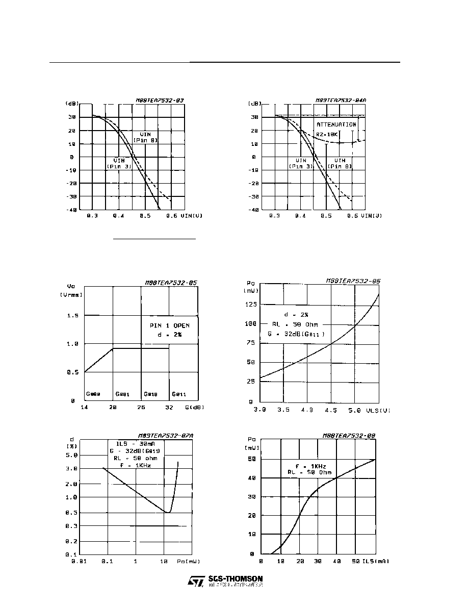
Figure 1 : Loudspeaker Gain Versus Voltage on
Pin (3) - (8) with Pin 2 Open.
Figure 3 : AC Output Voltage Versus Amplifier
Gain.
Figure 4 : Power Available on Loudspeaker
Versus V
LS
Typical Curve.
Figure 2 :LoudspeakerGain Versus Voltage on
Pin (3) - (8) and Versus R
2
. (*)
Zin2 (1.2 K)
R2 = 10 K
ATT = 20 dB
(*) ATTENUATION =
Zin2 (1.2 K) + R2 (E X T)
R2 = 3 K
ATT
10 dB
Figure 5 : Distortion Versus Output Power.
Figure 6 : Output Power Versus Supply Current.
TEA7532
4/16
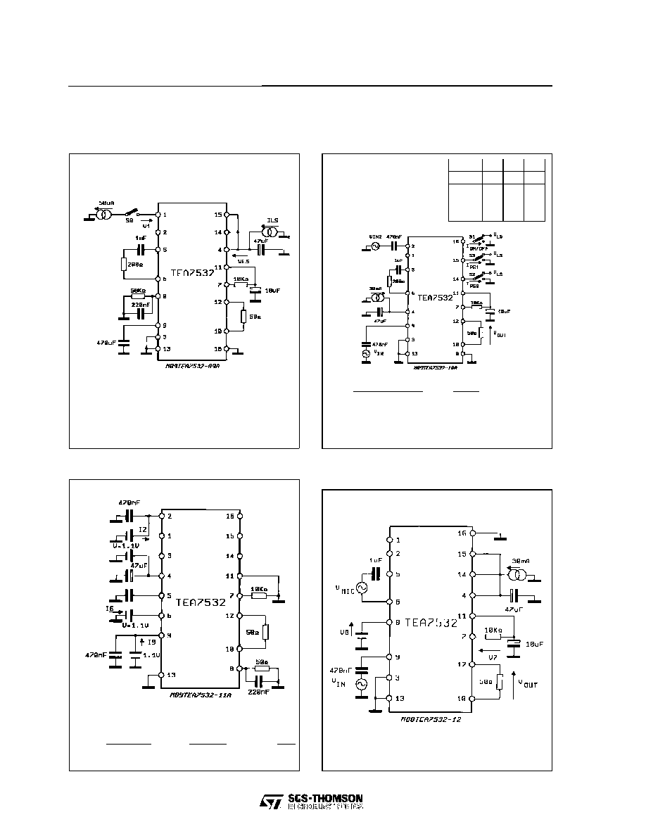
TEST CIRCUITS
Figure 7 : Shuntvoltage Regulator/ Reference
Voltage at Pin 1.
Note : S0 open for VLS 1
S0 close for VLSM.
Figure 8 : Loudspeaker Amplifier : Gain/Distor
tion/Output Offset.
V (10) V (12)
Vout
·
G =
=
V (9)
V (9)
·
VOFFS with Vin = 0.
V
LS
= 1
G
ND
= 0
Figure 9 : Impedance ZMIC, ZINP and Zin2.
1.1 V
1.1 V
1.1 V
Zmic =
; Zinp =
; Zin2 =
I6
I9
I2
Figure 10 : Antiacoustic Feedback System at
G011.
S1
S2
S3
G1XX
1
X
X
G000
0
0
0
G010
0
1
0
G001
0
0
1
TEA7532
5/16