TS5070
TS5071
PROGRAMMABLE CODEC/FILTER
COMBO 2
ND
GENERATION
COMPLETE CODEC AND FILTER SYSTEM
INCLUDING :
≠ TRANSMIT AND RECEIVE PCM CHANNEL
FILTERS
≠
µ
-LAW OR A-LAW COMPANDING CODER
AND DECODER
≠ RECEIVE POWER AMPLIFIER DRIVES
300
≠ 4.096 MHz SERIAL PCM DATA (max)
PROGRAMMABLE FUNCTIONS :
≠ TRANSMIT GAIN : 25.4 dB RANGE, 0.1 dB
STEPS
≠ RECEIVE GAIN : 25.4 dB RANGE, 0.1 dB
STEPS
≠ HYBRID BALANCE CANCELLATION FIL-
TER
≠ TIME-SLOT ASSIGNMENT: UP TO
64
SLOTS/FRAME
≠ 2 PORT ASSIGNMENT (TS5070)
≠ 6 INTERFACE LATCHES (TS5070)
≠ A OR
µ
-LAW
≠ ANALOG LOOPBACK
≠ DIGITAL LOOPBACK
DIRECT
INTERFACE
TO
SOLID-STATE
SLICs
SIMPLIFIES TRANSFORMER SLIC, SINGLE
WINDING SECONDARY
STANDARD SERIAL CONTROL INTERFACE
80 mW OPERATING POWER (typ)
1.5mW STANDBY POWER (typ)
MEETS OR EXCEEDS ALL CCITT AND
LSSGR SPECIFICATIONS
TTL AND CMOS COMPATIBLE DIGITAL IN-
TERFACES
DESCRIPTION
The TS5070 series are the second generationcom-
bined PCM CODEC and Filter devices optimized
for digital switching applications on subscriber and
trunk line cards.
Using advanced switched capacitor techniques the
TS5070 and TS5071 combine transmit bandpass
and receive lowpass channel filters with a com-
panding PCM encoder and decoder. The devices
are A-law and
µ
-law selectable and employ a con-
ventional serial PCM interface capable of being
clocked up to 4.096 MHz. A number of programma-
ble functions may be controlled via a serial control
port.
Channel gains are programmable over a 25.4 dB
range in each direction, and a programmable filter
is included to enable Hybrid Balancing to be ad-
justed to suit a wide range of loop impedance con-
ditions.
Both transformer and active SLIC interface circuits
with real or complex termination impedances can
be balanced by this filter, with cancellation in ex-
cess of 30 dB being readily achievable when meas-
ured across the passbandagainst standardtest ter-
mination networks.
To enable COMBO IIG to interface to the SLIC con-
trol leads, a number of programmable latches are
included ; each may be configured as either an in-
put or an output. The TS5070 provides 6 latches
and the TS5071 5 latches.
December 1997
DIP20 (Plastic)
ORDERING NUMBER:TS5071N
PLCC28
ORDERING NUMBERS: TS5070FN
TS5070FNTR
1/32
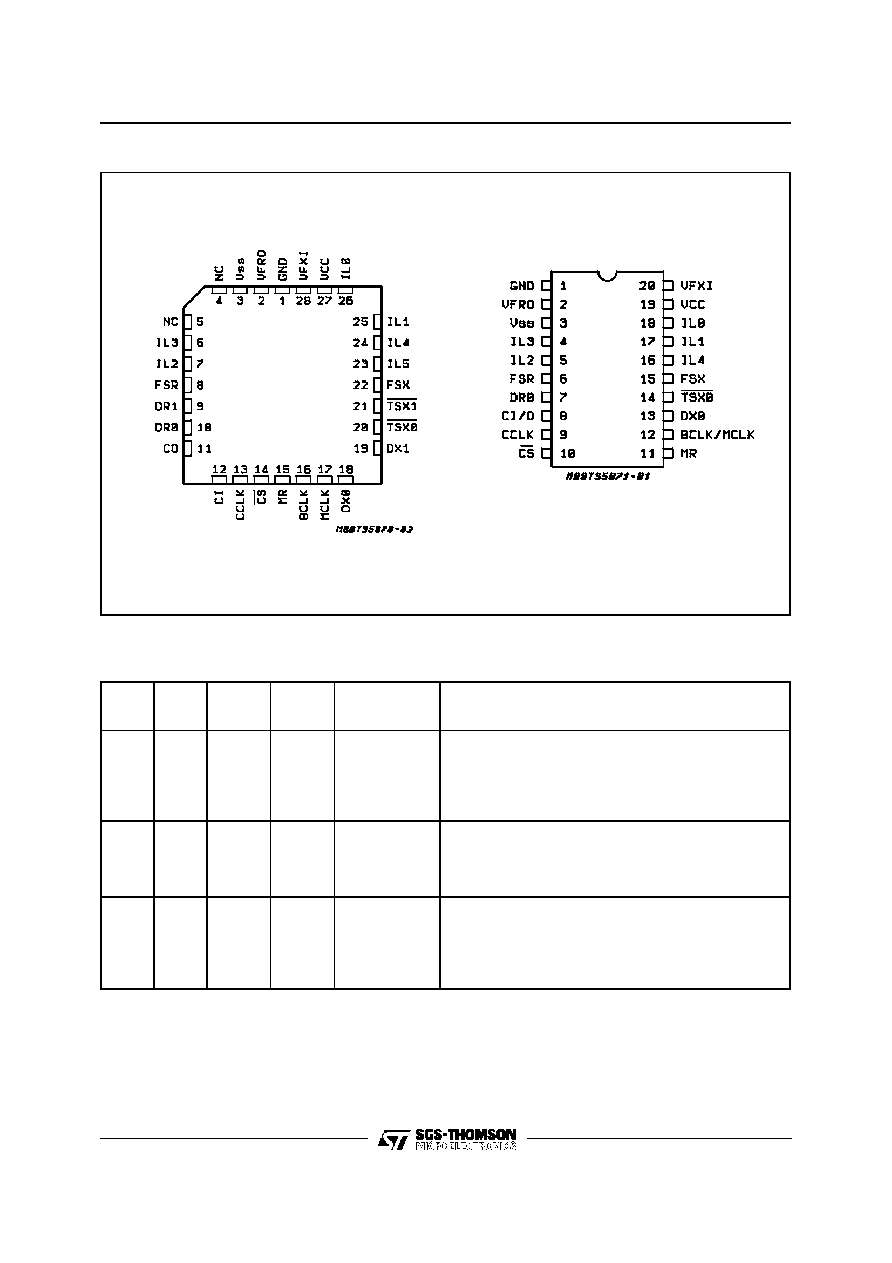
TS5070 PIN FUNCTIONALITY (PLCC28)
No.
Name
Function
1
GND
Ground Input (+0V)
2
VF
R
0
Analog Output
3
V
SS
Supply Input (-5V)
4
NC
Not Connected
5
NC
Not Connected
6
IL3
Digital Input or Output defined by LDR register content
7
IL2
Digital Input or Output defined by LDR register content
8
FS
R
Digital input
9
D
R
1
Digital input sampled by BCLK falling edge
10
D
R
0
Digital input sampled by BCLK falling edge
11
CO
Digital output (shifted out on CCLK rising edge)
12
CI
Digital input (sampled on CCLK falling edge)
13
CCLK
Digital input (clock)
14
CS
Digital input (chip select for CI/CO)
15
MR
Digital Input
16
BCLK
Digital input (clock)
17
MCLK
Digital input
18
D
X
0
Digital output clocked by BCLK rising edge
19
D
X
1
Digital output clocked by BCLK rising edge
20
TS
X
0
Open drain output (pulled low by active DX0 time slot)
21
TS
X
1
Open drain output (pulled low by active DX1 time slot)
22
FS
X
Digital input
23
IL5
Digital input or output defined by LDR register content
24
IL4
Digital input or output defined by LDR register content
25
IL1
Digital input or output defined by LDR register content
26
IL0
Digital input or output defined by LDR register content
27
V
CC
Supply input (+5V)
28
VF
X
I
Analog input
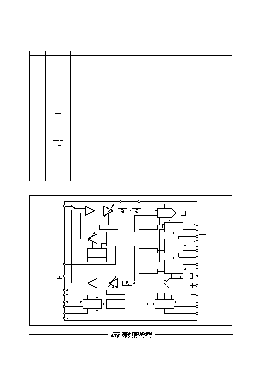
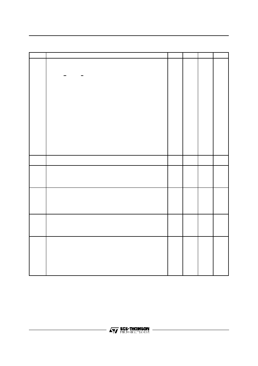
HYBRID
BALANCE
FILTER
ENCODER
TX GAIN
TX
REGISTER
TX TIME SLOT
Vref
HYBAL 1
HYBAL 2
HYBAL 3
TIME-SLOT
ASSIGNMENT
CTL REG.
RX TIME SLOT
RX
REGISTER
RX GAIN
DECODER
AZ
TS5070/71
INTERFACE
LATCHES
LATCH DIR
LATCH CONT.
CONTROL
INTERFACE
DX0
DX1
TSX0
TSX1
FSX
BCLK
FSR
DR0
DR1
MCLK
MR
CS
CCLK
CO
CI
VSS=-5V
VCC=+5V
VFXI
VFRO
GND
IL5
IL4
IL3
IL2
IL1
IL0
D94TL135
TS5070 FUNCTIONAL DIAGRAM
TS5070 - TS5071
2/32
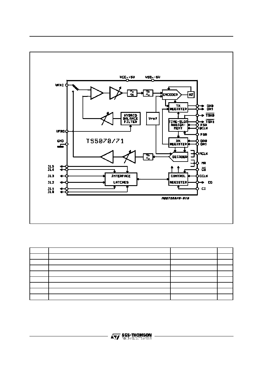
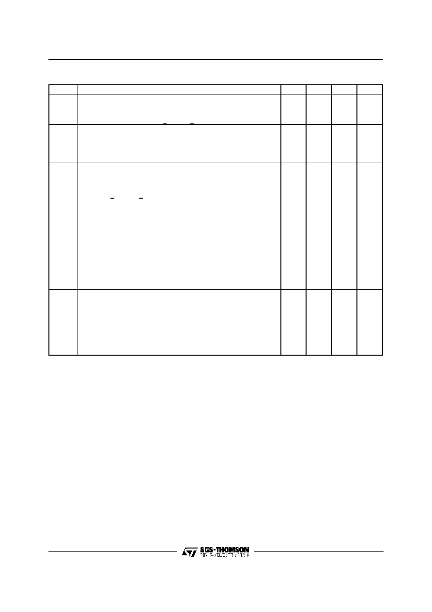
BLOCK DIAGRAM
ABSOLUTE MAXIMUM RATINGS
Symbol
Parameter
Value
Unit
V
CC
V
CC
to GND
7
V
V
SS
V
SS
to GND
≠ 7
V
Voltage at VFXI
V
CC
+ 0.5 to V
SS
≠ 0.5
V
V
IN
Voltage at Any Digital Input
V
CC
+ 0.5 to GND ≠ 0.5
V
Current at VFRO
±
100
mA
I
O
Current at Any Digital Output
±
50
mA
T
stg
Storage Temperature Range
≠ 65, + 150
∞
C
T
lead
Lead Temperature Range (soldering, 10 seconds)
300
∞
C
TS5070 - TS5071
3/32
PIN CONNECTIONS
POWER SUPPLY, CLOCK
Name
Pin
Type
TS5070
FN
TS5071
N
Function
Description
V
CC
V
SS
GND
S
S
S
27
3
1
19
3
1
Positive Power
Supply
Negative
Power Supply
Ground
+ 5 V
±
5 %
≠ 5 V
±
5 %
All analog and digital signals are referenced to this pin.
BCLK
I
16
12
Bit Clock
Bit clock input used to shift PCM data into and out of the
D
R
and D
X
pins. BCLK may vary from 64 kHz to 4.096
MHz in 8 kHz increments, and must be synchronous with
MCLK (TS5071 only).
MCLK
I
17
12
Master Clock
Master clock input used by the switched capacitor filters
and the encoder and decoder sequencing logic. Must be
512 kHz, 1. 536/1. 544 MHz,
2.048 MHz or 4.096 MHz and synchronous with BCLK.
BCLK and MCLK are wired together in the TS5071.
PLCC28
TS5070FN
DIP20
TS5071N
TS5070 - TS5071
4/32
TRANSMIT SECTION
Name
Pin
Type
TS5070
FN
TS5071
N
Function
Description
FS
X
I
22
15
Transmit
Frame Sync.
Normally a pulse or squarewave waveform with an 8 kHz
repetition rate is applied to this input to define the start of
the transmit time-slot assigned to this device (non-delayed
data mode) or the start of the transmit frame (delayed
data mode using the internal time-slot assignment
counter).
VF
X
I
I
28
20
Transmit
Analog
This is a high≠impedance input. Voice frequency signals
present on this input are encoded as an A≠law or
µ
≠law
PCM bit stream and shifted out on the selected D
X
pin.
D
X
0
D
X
1
0
0
18
19
13
≠
Transmit Data
D
X
1 is available on the TS5070 only, D
X
0 is available on
all devices. These transmit data TRI≠STATE
Æ
outputs
remain in the high impedance state except during the
assigned transmit time≠slot on the assigned port, during
which the transmit PCM data byte is shifted out on the
rising edges of BCLK.
TS
X
0
TS
X
1
0
0
20
21
14
≠
Transmit
Time≠slot
TS
X
1 is available on the TS5070 only.
TS
X
0 is available on all devices. Normally these opendrain
outputs are floating in a high impedance state except
when a time≠slot is active on one of the D
X
outputs, when
the apppropriate TS
X
output pulls low to
enable a backplane line≠driver. Should be strapped to
ground (GND) when not used.
RECEIVE SECTION
Name
Pin
Type
TS5070
FN
TS5071
N
Function
Description
FS
R
I
8
6
Receive Frame
Sync.
Normally a pulse or squarewave waveform with an 8 kHz
repetition rate is applied to this input to define the start of
the receive time≠slot assigned to this device (non-delayed
frame mode) or the start of the receive frame (delayed
frame mode using the internal time-slot assignment
counter.
VF
R
0
0
2
2
Receive Analog
The receive analog power amplifier output, capable of
driving load impedances as low as 300
(depending on
the peak overload level required). PCM data received on
the assigned D
R
pin is decoded and appears at this output
as voice frequency signals.
D
R
0
D
R
1
I
I
10
9
7
≠
Receive Data
D
R
1 is available on the TS5070 only, D
R
0 is available on
all devices. These receive data input(s) are inactive
except during the assigned receive time≠slot of the
assigned port when the receive PCM data is shifted in on
the falling edges of BCLK.
TS5070 - TS5071
5/32
FUNCTIONAL DESCRIPTION
POWER-ON INITIALIZATION
When power is first applied, power-on reset cir-
cuitry initializes COMBO IIG and puts it into the
power-down state. The gain control registers for
the transmit and receive gain sections are pro-
grammed for no output, the hybrid balance circuit
is turned off, the power amp is disabled and the
device is in the non-delayed timing mode. The
Latch Direction Register (LDR) is pre-set with all
IL pins programmed as inputs, placing the SLIC
interface pins in a high impedance state. The
CI/O pin is set as an input ready for the first con-
trol byte of the initialization sequence. Other initial
states in the Control Register are indicated in Ta-
ble 2.
A reset to these same initial conditions may also be
forced by driving the MR pin momentarilyhigh. This
may be done either when powered-up or down. For
normal operation this pin must be pulled low. If not
used, MR should be hard-wired to ground.
The desired modes for all programmable functions
may be initialized via the control port prior to a
Power-up command.
INTERFACE, CONTROL, RESET
Name
Pin
Type
TS5070
FN
TS5071
N
Function
Description
IL5
IL4
IL3
IL2
IL1
IL0
I/O
I/O
I/O
I/O
I/O
I/O
23
24
6
7
25
26
≠
16
4
5
17
18
Interface
Latches
IL5 through IL0 are available on the TS5070,
IL4 through IL0 are available on the TS5071.
Each interface Latch I/O pin may be individually
programmed as an input or an output determined by the
state of the corresponding bit in the Latch Direction
Register (LDR) . For pins configured as inputs, the logic
state sensed on each input is latched into the interface
Latch Register (ILR) whenever control data is written to
COMBO IIG, while CS is low, and the information is
shifted out on the CO (or CI/O) pin. When configured as
outputs, control data written into the ILR appears at the
corresponding IL pins.
CCLK
I
13
9
Control Clock
This clock shifts serial control information into or out of CI
or CO (or CI/O) when the CS input is low depending on
the current instruction. CCLK may be asynchronous with
the other system clocks.
CI/O
I/O
≠
8
Control Data
Input/output
This is Control Data I/O pin wich is provided on the
TS5071. Serial control information is shifted into or out of
COMBO IIG on this pin when CS is low. The direction of
the data is determined by the current instruction as defined
in Table 1.
CI
CO
I
O
12
11
≠
≠
Control Data
Input
Control Data
Output
These are separate controls, availables only on the
TS5070. They can be wired together if required.
CS
I
14
10
Chip Select
When this pins is low, control information can be written to
or read from the COMBO IIG via the CI and CO pins (or
CI/O).
MR
I
15
11
Master Reset
This logic input must be pulled low for normal operation of
COMBO IIG. When pulled momentarily high, all
programmable registers in the device are reset to the
states specified under "Power≠on Initialization".
TS5070 - TS5071
6/32

POWER-DOWN STATE
Following a period of activity in the powered-up
state the power-down state may be re-entered by
writing any of the control instructions into the serial
control port with the "P" bit set to "1" It is recom-
mended that the chip be powered down before writ-
ing any additional instructions. In the power-down
state, all non-essential circuitry is de-activated and
the D
X
0 and D
X
1 outputs are in the high impedance
TRI-STATE condition.
The coefficients stored in the Hybrid Balance circuit
and the Gain Control registers, the data in the LDR
and ILR, and all control bits remain unchanged in
the power-down state unless changed by writing
new data via the serial control port, which remains
operational. The outputs of the Interface Latches
also remain active, maintaining the ability to moni-
tor and control a SLIC.
TRANSMIT FILTER AND ENCODER
The Transmit section input, VF
X
I, is a high imped-
ance summing input which is used as the differenc-
ing point for the internal hybrid balancecancellation
signal. No external components are needed to set
the gain. Following this circuit is a programmable
gain/attenuationamplifier which is controlled by the
contents of the Transmit Gain Register (see Pro-
grammable Functions section). An active prefilter
then precedes the 3rd order high-pass and 5th or-
der low-pass switched capacitor filters. The A/D
converter has a compressingcharacteristic accord-
ing to the standard CCITT A or
µ
255 coding laws,
which must be selected by a control instruction dur-
ing initialization (see table 1 and 2). A precision on-
chip voltage reference ensures accurate and highly
stable transmission levels. Any offset voltage aris-
ing in the gain-set amplifier, the filters or the com-
parator is cancelled by an internal auto-zero circuit.
Each encode cycle begins immediately following
the assigned Transmit time-slot. The total signal
delay referenced to the start of the time-slot is ap-
proximately 165
µ
s (due to the Transmit Filter)
plus 125
µ
s (due to encoding delay), which totals
290
µ
s. Data is shifted out on D
X
0 or D
X
1 during
the selected time slot on eight rising edges of
BCLK.
DECODER AND RECEIVE FILTER
PCM data is shifted into the Decoder's Receive
PCM Register via the D
R
0 or D
R
1 pin during the se-
lected time-slot on the 8 fallingedges of BCLK. The
Decoder consists of an expanding DAC with either
A or
µ
255 law decoding characteristic, which is se-
lected by the same control instruction used to select
the Encode law during initialization. Following the
Decoder is a 5th order low-pass switched capacitor
filter with integral Sin x/x correction for the 8 kHz
sample and hold. A programmable gain amplifier,
which must be set by writing to the Receive Gain
Register, is included, and finally a Post-Filter/Power
Amplifier capable of driving a 300
load to
±
3.5
V, a 600
load to
±
3.8 V or 15 k
load to
±
4.0 V
at peak overload.
A decode cycle begins immediately after each re-
ceive time-slot, and 10
µ
s later the Decoder DAC
output is updated. The total signal delay is 10
µ
s
plus 120
µ
s (filter delay) plus 62.5
µ
s (1/2 frame)
which gives approximately 190
µ
s.
PCM INTERFACE
The FS
X
and FS
R
frame sync inputs determine the
beginning of the 8-bit transmit and receive time-
slots respectively. They may have any duration
from a single cycle of BCLK to one MCLK period
LOW. Two different relationships may be estab-
lished betweenthe framesync inputs and theactual
time-slots on the PCM busses by setting bit 3 in the
Control Register (see table 2). Non delayed data
mode is similar to long-frame timing on the
ETC5050/60 series of devices : time-slots being
nominally coincident with the rising edge of the ap-
propriate FS input. The alternative is to use De-
layed Data mode which is similar to short-frame
sync timing, in which each FS input must be high
at least a half-cycle of BCLK earlier than the time-
slot.
The Time-Slot Assignment circuit on the device can
only be used with Delayed Data timing. When using
Time-Slot Assignment, the beginning of the first
time-slot in a frame is identified by the appropriate
FS input. The actual transmit and receive time-slots
are then determined by the internal Time-Slot As-
signment counters. Transmit and Receive frames
and time-slots may be skewed from each other by
any number of BCLK cycles.
During each assigned transmit time-slot, the se-
lected D
X
0/1 output shifts data out from the PCM
register on the rising edges of BCLK. TS
X
0 (or
TS
X
1 as appropriate) also pulls low for the first 7
1/2 bit times of the time-slot to control the TRI-
STATE Enable of a backplane line driver. Serial
PCM data is shifted into the selected D
R
0/1 input
during each assigned Receive time slot on the
falling edges of BCLK. D
X
0 or D
X
1 and D
R
0 or
D
R
1 are selectable on the TS5070 only.
SERIAL CONTROL PORT
Control information and data are written into or
readback from COMBO IIG via the serial control
port consisting of the control clock CCLK ; the serial
data input/ou tput CI/O (or separate input CI, and
output CO on the TS5070 only) ; and the Chip Se-
lect input CS. All control instructions require 2
bytes,as listed in table 1, with the exceptionof a sin-
gle byte power-up/down command. The byte 1 bits
are used as follows: bit 7 specifies power-up or
power-down; bits 6, 5, 4 and 3 specify the register
address; bit 2 specifies whether the instructions is
read or write; bit 1 specifies a one or two byte in-
TS5070 - TS5071
7/32
struction; and bit 0 is not used. To shift control data
into COMBO IIG, CCLK must be pulsed high 8
times while CS is low. Data on the CI or CI/O input
is shifted into the serial input register on the falling
edge of each CCLK pulse. After all data is shifted
in, the content s of the input shift register are de-
coded, and may indicate that a 2nd byte of control
data will follow. This second byte may either be de-
fined by a secondbyte-wide CS pulse or may follow
the first continuously,i.e. it is not mandatory for CS
to return high in between the first and second con-
trol bytes. On the falling edge of the 8
th
CCLK clock
pulse in the 2nd control byte the data is loaded into
the appropriateprogrammable register. CS may re-
main low continuously when programming succes-
sive registers, if desired.However CS shouldbe set
high when no data transfers are in progress.
To readbackinterface Latch data or status informa-
tion from COMBO IIG, the first byte of the appropri-
ate instruction is strobed in during the first CS pulse,
as defined in table 1. CS must then be taken low for
a further 8 CCLK cycles, during which the data is
shifted onto the CO or CI/O pin on the rising edges
of CCLK. When CS is high the CO or CI/O pin is in
the high-impedanceTRI-STATE, enabling the CI/O
pins of many devices to be multiplexed together.
Thus, to summarize, 2-byte READ and WRITE in-
structions may use either two 8-bit wide CS pulses
or a single 16-bit wide CS pulse.
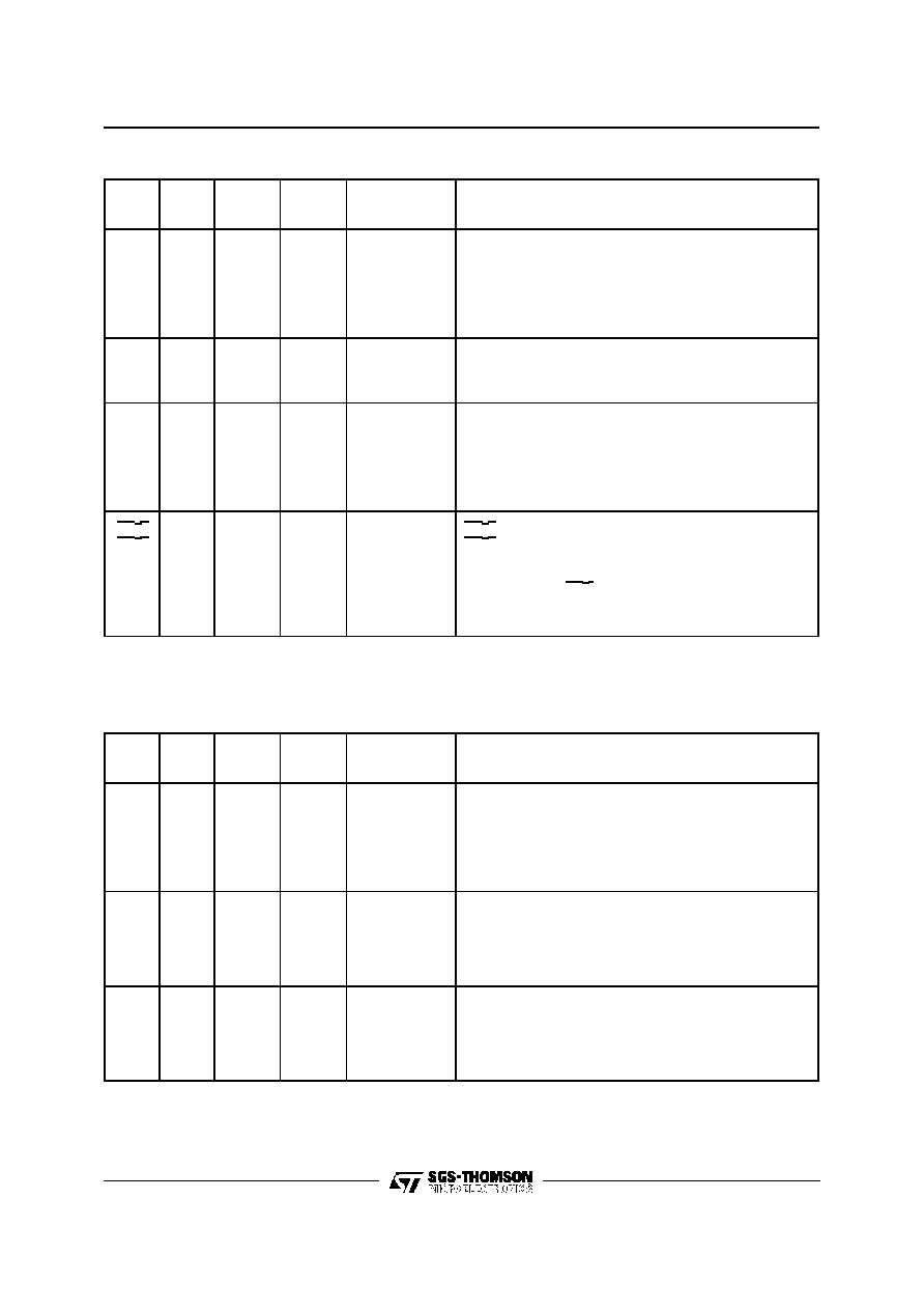
Function
Byte 1
Byte 2
7
6
5
4
3
2
1
0
Single Byte Power≠up/down
P
X
X
X
X
X
0
X
None
Write Control Register
Read≠back Control Register
P
P
0
0
0
0
0
0
0
0
0
1
1
1
X
X
See Table 2
See Table 2
Write Latch Direction Register (LDR)
Read Latch Direction Register
P
P
0
0
0
0
1
1
0
0
0
1
1
1
X
X
See Table 4
See Table 4
Write Latch Content Register (ILR)
Read Latch Content Register
P
P
0
0
0
0
0
0
1
1
0
1
1
1
X
X
See Table 5
See Table 5
Write Transmit Time≠slot/port
Read≠back Transmit Time≠slot/port
P
P
1
1
0
0
1
1
0
0
0
1
1
1
X
X
See Table 6
See Table 6
Write Receive Time≠slot/port
Read≠back Receive Time≠slot/port
P
P
1
1
0
0
0
0
1
1
0
1
1
1
X
X
See Table 6
See Table 6
Write Transmit Gain Register
Read Transmit Gain Register
P
P
0
0
1
1
0
0
1
1
0
1
1
1
X
X
See Table 7
See Table 7
Write Receive Gain Register
Read Receive Gain Register
P
P
0
0
1
1
0
0
0
0
0
1
1
1
X
X
See Table 8
See Table 8
Write Hybrid Balance Register
1
Read Hybrid Balance Register
1
P
P
0
0
1
1
1
1
0
0
0
1
1
1
X
X
See Table 9
See Table 9
Write Hybrid Balance Register
2
Read Hybrid Balance Register
2
P
P
0
0
1
1
1
1
1
1
0
1
1
1
X
X
See Table 10
See Table 10
Write Hybrid Balance Register
3
Read Hybrid Balance Register
3
P
P
1
1
0
0
0
0
0
0
0
1
1
1
X
X
Table 1: Programmable Register Instructions
PROGRAMMABLE FUNCTIONS
POWER-UP/DOWN CONTROL
Following power-on initialization, power-up and
power-down control may be accomplished by
writing any of the control instructions listed in ta-
ble 1 into COMBO IIG with the "P" bit set to "0"
for power-up or "1" for power-down. Normally it is
recommended that all programmable functions be
initially programmed while the device is powered
down. Power state control can then be included
with the last programming instruction or the sepa-
rate single-byte instruction. Any of the program-
mable registers may also be modified while the
device is powered-up or down be setting the "P"
bit as indicated. When the power up or down con-
trol is entered as a single byte instruction, bit one
(1) must be set to a 0.
When a power-up command is given, all de-acti-
vated circuits are activated, but the TRI-STATE
PCM output(s), D
X
0 (and D
X
1), will remain in the
high impedance state until the second FS
X
pulse
after power-up.
Notes: 1. Bit 7 of bytes 1 and 2 is always the first bit clocked into or out of the CI, CO or CI/CO pin.
2. "P" is the power-up/down control bit, see "Power-up" section ("0" = Power Up "1" = Power Down).
TS5070 - TS5071
8/32
CONTROL REGISTER INSTRUCTION
The first byte of a READ or WRITE instruction to
the Control Register is as shown in table 1. The
second byte functions are detailed in table 2.
MASTER CLOCK FREQUENCY SELECTION
A Master clock must be provided to COMBO IIG
for operation of the filter and coding/decoding
functions. The MCLK frequency must be either
512 kHz, 1.536 MHz, 1.544 MHz, 2.048 MHz, or
4.096 MHz and must be synchronous with BCLK.
Bits F1 and F0 (see table 2) must be set during
initialization to select the correct internal divider.
CODING LAW SELECTION
Bits "MA" and "IA" in table 2 permit the selection
of
µ
255 coding or A-law coding with or without
even-bit inversion.
ANALOG LOOPBACK
Analog Loopback mode is entered by setting the
"AL" and "DL" bits in the Control Register as shown
in table 2. In the analog loopback mode, the Trans-
mit input VF
X
I is isolated from the input pin and in-
ternally connected to the VF
R
O output, forming a
loop from the Receive PCM Register back to the
Transmit PCM Register. The VF
R
O pin remains ac-
tive, and the programmed settings of the Transmit
and Receive gains remain unchanged, thus care
must be taken to ensure that overload levels are
not exceeded anywhere in the loop.
Hybrid balancing must be disabled for meaning
ful analog loopback Function.
DIGITAL LOOPBACK
Digital Loopback mode is entered by setting the
"DL" bit in the Control Register as shown in table 2.
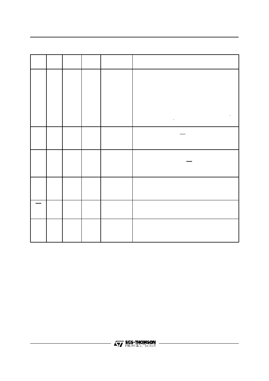
Bit Number
Fun ction
7
6
5
4
3
2
1
0
F1
F0
MA
IA
DN
DL
AL
PP
0
0
1
1
0
1
0
1
MCLK = 512 kHz
MCLK = 1. 536 or 1. 544 MHz
MCLK = 2. 048 MHz
*
MCLK = 4. 096 MHz
0
1
1
X
0
1
Select
µ
. 255 Law
*
A≠law, Including Even Bit Inversion
A≠Law, No Even Bit Inversion
0
1
Delayed Data Timing
Non≠delayed Data Timing
*
0
1
0
0
X
1
Normal Operation
*
Digital Loopback
Analog Loopback
0
1
Power Amp Enabled in PDN
Power Amp Disabled in PDN
*
Table 2: Control Register Byte 2 Functions
Table 3: Coding Law Conventions.
m255 Law
MSB LSB
True A-law with
even bit inversion
MSB LSB
A-law without
even bit inversion
MSB LSB
V
IN
= +Full Scale
1
0
0
0
0
0
0
0
1
0
1
0
1
0
1
0
1
1
1
1
1
1
1
1
V
IN
= 0V
1
0
1
1
1
1
1
1
1
1
1
1
1
1
1
1
1
0
1
1
0
0
1
1
0
0
1
1
0
0
1
1
1
0
0
0
0
0
0
0
0
0
0
0
0
0
0
0
V
IN
= -Full Scale
0
0
0
0
0
0
0
0
0
0
1
0
1
0
1
0
0
1
1
1
1
1
1
1
Note: The MSB is always the first PCM bit shifted in or out of COMBO IIG.
(*) State at power-on initialization (bit 4 = 0)
TS5070 - TS5071
9/32
This mode provides another stage of path verifica-
tion by enabling data written into the Receive PCM
Register to be read back from that register in any
Transmit time-slot at D
X
0 or D
X
1.
For Analog Loopback as well as for Digital Loop-
back PCM decoding continues and analog output
appears at VF
R
O. The output can be disabled by
pro gramming "No Output" in the Receive Gain
Register (see table 8).
INTERFACE LATCH DIRECTIONS
Immediately following power-on, all Interface
Latches assume they are inputs, and therefore all
IL pins are in a high impedance state. Each IL pin
may be individually programmed as a logic input or
output by writing the appropriate instruction to the
LDR, see table 1 and 4. Bits L
5
-L
0
must be set by
writing the specific instruction to the LDR with the
L bits in the second byte set as specified in table 4.
Unused interface latches should be programmed
as outputs. For the TS5071, L5 should always be
programmed as an output.
(*) State at power-on initilization.
Note: L5 should be programmed as an output for the TS5071.
INTERFACE LATCH STATES
Interface Latches configured as outputs assume
the state determined by the appropriate data bit in
the 2-byte instruction written to the Latch Content
Register (ILR) as shown in tables 1 and 5.
Latches configured as inputs will sense the state
applied by an external source, such as the Off-
Hook detect output of a SLIC. All bits of the ILR,
i.e. sensed inputs and the programmed state of
outputs, can be read back in the 2nd byte of a
READ from the ILR. It is recommended that, dur-
ing initialization, the state of IL pins to be config-
ured as outputs should first be programmed, fol-
lowed
immediately
by
the
Latch
Direction
Register.
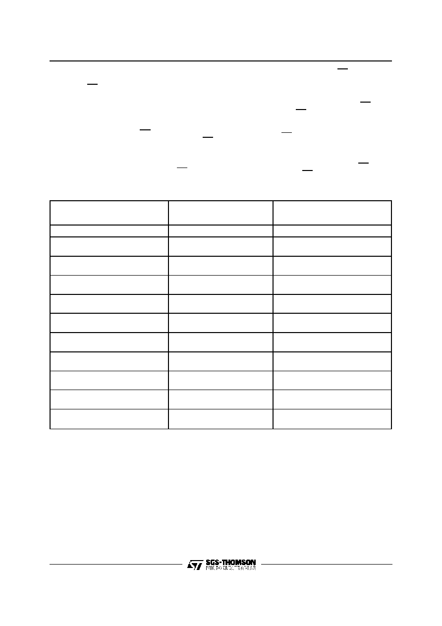
TIME-SLOT ASSIGNMENT
COMBO IIG can operate in either fixed time-slot or
time-slot assignment mode for selecting the Trans-
mit and Receive PCM time-slots. Following power-
on, the deviceis automaticallyin Non-Delayed Tim-
ing mode, in which the time-slot always begins with
the leading (rising) edge of frame sync inputs FS
X
and FS
R
. Time-Slot Assignment may only be used
with Delayed Data timing : see figure 6. FS
X
and
FS
R
may have any phase relationship with each
other in BCLK period increments.
Bit Number
7
6
5
4
3
2
1
0
L0
L1
L2
L3
L4
L5
X
X
Table 4: Byte 2 Function of Latch Direction Register
L
N
Bit
IL Direction
0
1
Input
*
Output
Bit Number
Function
7
EN
6
PS
(note 1)
5
T5
(note 2)
4
T4
3
T3
2
T2
1
T1
0
T0
0
X
X
X
X
X
X
X
Disable D
X
Outputs (transmit instruction) *
Disable D
R
Inputs (receive instruction) *
1
0
Assign One Binary Coded Time-slot from 0≠63
Assign One Binary Coded Time-slot from 0≠63
Enable D
X
0 Output, Disable D
X
1 Output
(Transmit instruction)
Enable D
R
0 Input, Disable D
R
1 Input
(Receive Instruction)
1
1
Assign One Binary Coded Time-slot from 0≠63
Assign One Binary Coded Time-slot from 0≠63
Enable D
X
1 Output, Disable D
X
0 Output
(Transmit instruction)
Enable D
R
1 Input, Disable D
R
0 Input
(Receive Instruction)
Table 6: Byte 2 of Time-slot and Port Assignment Instructions
Bit Number
7
6
5
4
3
2
1
0
D0
D1
D2
D3
D4
D5
X
X
Table 5: Interface Latch Data Bit Order
Notes:
1. The "PS" bit MUST always be set to 0 for the TS5071.
2. T5 is the MSB of the time-slot assignment.
(*) State at power-on initialization
TS5070 - TS5071
10/32
Alternatively, the internal time-slot assignment
counters and comparators can be used to access
any time-slot in a frame,using the framesync inputs
as marker pulses for the beginning of transmit and
receive time-slot 0. In this mode, a frame may con-
sist of up to 64 time-slots of 8 bits each. A time-slot
is assignedby a 2-byte instructionas shown in table
1 and 6. The last 6 bits of the second byte indicate
the selected time-slot from 0-63 using straight bi-
nary notation. A new assignment becomes active
on the second frame following the end of the Chip
Select for the second control byte. The "EN" bit al-
lows the PCM inputs D
R
0/1 or outputs D
X
0/1 as ap-
propriate, to be enabled or disabled.
Time-Slot Assignment mode requires that the FS
X
and FS
R
pulses must conform to the delayed timing
format shown in figure 6.
PORT SELECTION
On the TS5070 only, an additional capability is
available : 2 Transmit serial PCM ports, D
X
0 and
D
X
1, and 2 receive serial PCM ports, D
R
0 and D
R
1,
are provided to enable two-way space switching to
be implemented. Port selections for transmit and
receive are made within the appropriate time-slot
assignmentinstruction using the "PS" bit in the sec-
ond byte.
On the TS5071, only ports D
X
0 and D
R
0 are avail-
able, therefore the "PS" bit MUST always be set to
0 for these devices.
Table 6 shows the format for the second byte of
both transmit and receive time-slot and port assign-
ment instructions.
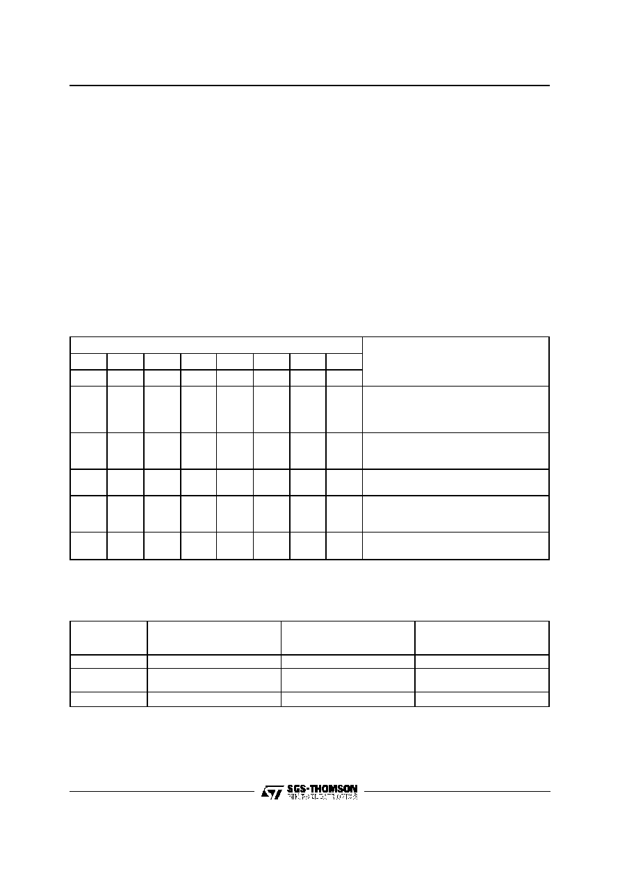
TRANSMIT GAIN INSTRUCTION BYTE 2
The transmit gain can be programmed in 0.1 dB
steps by writing to the Transmit Gain Register as
defined in tables 1 and 7. This corresponds to a
range of 0 dBm0 levels at VF
X
I between 1.619
Vrms and 0.087 Vrms (equivalent to + 6.4 dBm to
≠ 19.0 dBm in 600
).
To calculate the binary code for byte 2 of this in-
struction for any desired input 0 dBm0 level in
Vrms, take the nearest integer to the decimal
number given by :
and convert to the binary equivalent. Some exam-
ples are given in table 7.
Bit Number
0dBm0 Test Leve at VF
X
I
7
6
5
4
3
2
1
0
In dBm (Into 600
)
In Vrms (approx.)
0
0
0
0
0
0
0
0
No Output
0
0
0
0
0
0
0
0
0
0
0
0
0
1
1
0
≠ 19
≠ 18.9
0.087
0.088
1
0
1
1
1
1
1
1
0
0.775
1
1
1
1
1
1
1
1
1
1
1
1
1
1
0
1
+6.3
+6.4
1.60
1.62
Table 7: Byte 2 of Transmit Gain Instructions.
(*) State at power initialization
RECEIVE GAIN INSTRUCTION BYTE 2
The receive gain can be programmed in 0.1 dB
steps by writing to the Receive Gain Register as de-
fined in table 1 and 8. Note the following restriction
on output drive capability :
a) 0 dBm0 levels
8.1dBm at VF
R
O may be
driven into a load of
15 k
to GND,
b) 0 dBm0 levels
7.6dBm at VF
R
O may be
driven into a load of
600
to GND,
c) 0 dBm levels
6.9dBm at VF
R
O may be driven
into a load of
300
to GND.
To calculate the binary code for byte 2 of this in-
struction for any desired output 0 dBm0 level in
Vrms, take the nearest integer to the decimal num-
ber given by :
a
n
d convert to the binary equivalent. Some exam-
ples are given in table 8.
200 X log
10
(V/
6
) + 191
200 X log
10
(V/
6
) + 174
TS5070 - TS5071
11/32
HYBRID BALANCE FILTER
The Hybrid Balance Filter on COMBO IIG is a
programmable filter consisting of a second-order
Bi-Quad section, Hybal1, followed by a first-order
section, Hybal2, and a programmable attenuator.
Either of the filter sections can be bypassed if
only one is required to achieve good cancellation.
A selectable 180 degree inverting stage is in-
cluded to compensate for interface circuits which
also invert the transmit input relative to the re-
ceive output signal. The Bi-Quad is intended
mainly to balance low frequency signals across a
transformer SLIC, and the first order section to
balance midrange to higher audio frequency sig-
nals. The attenuator can be programmed to com-
pensate for VF
R
O to VF
X
I echos in the range
of -2.5 to ≠ 8.5 dB.
As a Bi-Quad, Hybal1 has a pair of low frequency
zeroes and a pair of complex conjugate poles.
When configuring the Bi-Quad, matching the
phase of the hybrid at low to midband frequencies
is most critical. Once the echo path is correctly
balanced in phase, the magnitude of the cancella-
tion signal can be corrected by the programmable
attenuator.
The Bi-Quad mode of Hybal1 is most suitable for
balancing interfaces with transformers having high
inductance of 1.5 Henries or more. An alternative
configuration for smaller transformers is available
by converting Hybal1 to a simple first-order section
with a single real low frequency pole and 0 Hz zero.
In this mode, the pole/zero frequency may be pro-
grammed.
Many line interfaces can be adequately balanced
by use of the Hybal1 section only, in which case
the Hybal2 filter should be de-selected to bypass
it.
Hybal2, the higher frequency first-order section, is
provided for balancing an electronic SLIC, and is
also helpful with a transformer SLIC in providing
additional phase correction for mid and high-band
frequencies, typically 1 kHz to 3.4 kHz. Such a
correction is particularly useful if the test balance
impedance includes a capacitor of 100 nF or less,
such as the loaded and non-loaded loop test net-
works in the United States. Independent place-
ment of the pole and zero location is provided.
Bit
State
Function
7
0
Disable Hybrid Balance Circuit Completely.
No internal cancellation is provided.
*
1
Enable Hybrid Balance Cancellation Path
6
0
Phase of the internal cancellation signal assumes inverted phase of the echo
path from VF
R
O to VF
X
I.
1
Phase of the internal cancellation signal assumes no phase inversion in the line
interface.
5
0
Bypass Hybal 2 Filter Section
1
Enable Hybal 2 Filter Section
G4≠G0
Attenuation Adjustment for the Magnitude of the Cancellation Signal. Range is
≠ 2.5 dB (00000) to ≠ 8.5 dB (11000)
Table 9: Hybrid Balance Register 1 Byte 2 Instruction.
Notes:
1. Maximum level into 300
; 2. Maximum level into 600
;
3. R
L
15K
(*) State at power on initialization
(*) State at power on initialization
Setting = Please refer to software TS5077 2
Bit Number
0dBm0 Test Leve at VF
R
0
7
6
5
4
3
2
1
0
In dBm (Into 600
)
In Vrms (approx.)
0
0
0
0
0
0
0
0
No Output
0
0
0
0
0
0
0
0
0
0
0
0
0
1
1
0
≠ 17.3
≠ 17.2
0.106
0.107
1
0
1
0
1
1
1
0
0
0.775
1
1
1
1
0
0
1
1
+ 6.9 (note 1)
1.71
1
1
1
1
1
0
1
0
+ 7.6 (note 2)
1.86
1
1
1
1
1
1
1
1
+ 8.1 (note 3)
1.07
Table 8: Byte 2 of Receive Gain Instructions.
TS5070 - TS5071
12/32
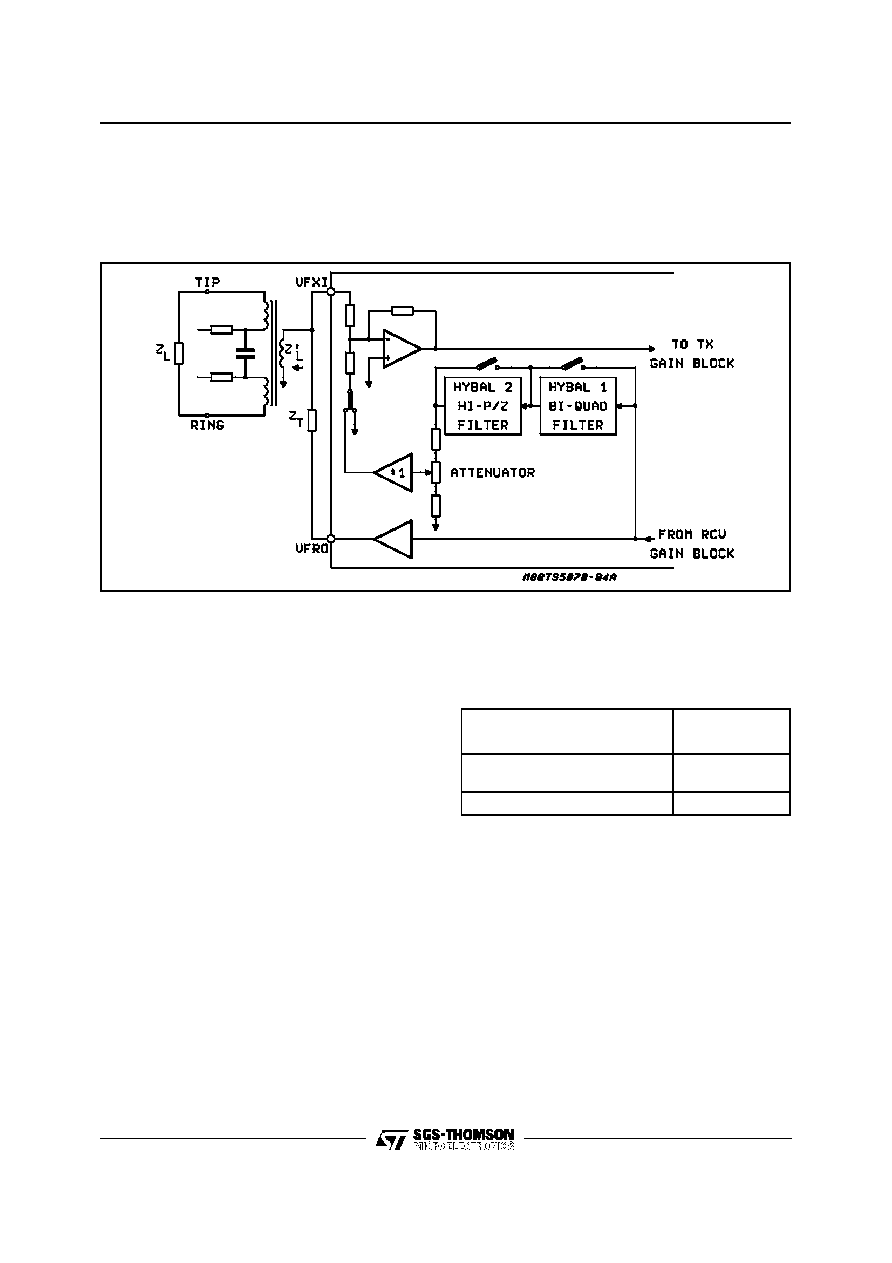
Figure 1 shows a simplified diagram of the local
echo path for a typical application with a trans-
former interface. The magnitude and phase of the
local echo signal, measured at VF
X
I, are a function
of the termination impedance Z
T
, the line trans-
former and the impedanceof the 2 W loop, Z
L
. If the
impedance reflected back into the transformer pri-
mary is expressed as Z
L
' then the echo path trans-
fer function from VF
R
O to VF
X
I is :
H(W) = Z
L
' /(Z
T
+ Z
L
')
(1)
Figure 1: Simplified Diagram of Hybrid Balance Circuit
PROGRAMMING THE FILTER
On initial power-up the Hybrid Balance filter is dis-
abled. Before the hybrid balance filter can be pro-
grammed it is necessary to design the transformer
and terminationimpedance in orderto meet system
2 W input return loss specifications, which are nor-
mally measured against a fixed test impedance
(600 or 900
in most countries). Only then can the
echo path be modeled and the hybrid balance filter
programmed. Hybrid balancing is also measured
against a fixed test impedance, specified by each
national Telecom administration to provide ade-
quate control of talker and listener echo over the
majority of their network connections. This test im-
pedance is Z
L
in figure 1. The echo signal and the
degree of transhybrid loss obtained by the pro-
grammable filter must be measured from the PCM
digital input D
R
0, to the PCM digital output D
X
0,
either by digital test signal analysis or by conversion
back to analog by a PCM CODEC/Filter.
Three registers must be programmed in COMBO
IIG to fully configure the Hybrid Balance Filter as
follows :
Register 1: select/de-select Hybrid Balance Filter;
invert/non-invert cancellation signal;
select/de-select Hybal2 filter section;
attenuatorsetting.
Register 2: select/de-select Hybal1 filter;
set Hybal1 to Bi-Quad or 1st order;
program pole and zero frequency.
Register 3 : program pole frequency in Hybal2 filter;
program zero frequencyin Hybal2 filter;
settings = Please refer to software
TS5077-2.
Standard filter design techniques may be used to
model the echo path (see equation (1)) and design
a matching hybrid balance filter configuration.Alter-
natively, the frequency response of the echo path
can be measured and the hybrid balance filter pro-
grammed to replicate it.
An Hybrid Balance filter design guide and soft-
ware optimization program are available under li-
cense from SGS-THOMSON Microelectronics (or-
der TS5077-2).
Bit Number
Function
7
6
5
4
3
2
1
0
0
0
0
0
0
0
0
0
By Pass Hybal 1
Filter
X
X
X
X
X
X
X
X
Pole/zero Setting
Table 10: Hybrid Balance Register 2 Byte 2 in-
structions
TS5070 - TS5071
13/32

APPLICATION INFORMATION
Figure 2 shows a typical application of the TS5070
together with a transformer SLIC.
The design of the transformer is greatly simplified
due to the on-chip hybrid balance cancellation filter.
Only one single secondary winding is required (see
application note AN.091 - Designing a subscriber
line card module using the TS5070/COMBO IIG).
Figures 3 and 4 show an arrangement with SGS-
Thomson monolithic SLICS.
POWER SUPPLIES
While the pins of the TS5070 and TS5071/COMBO
IIG devices are well protected against electrical
misuse, it is recommended that the standard
CMOS practice of applying GND to the device be-
fore any otherconnectionsare made shouldalways
be followed.In applicationswhere the printedcircuit
card may be plugged into a hot socket with power
and clocks already present, an extra long ground
pin on the connector should be used and a Schottky
diode connected between V
SS
and GND. To mini-
mize noise sources all ground connections to each
device should meet at a common point as close as
possible to the GND pin in order to prevent the in-
teraction of ground return currents flowing through
a common bus impedance. Power supply decou-
pling capacitors of 0.1
µ
F shouldbe connectedfrom
this common device ground point to V
CC
and V
SS
as closeto thedevice pins as possible. V
CC
and V
SS
should also be decoupled with low effective series
resis-tance capacitorsof at least 10
µ
F locatednear
the card edge connector.
TS5070 - TS5071
14/32
Figure 2: Transformer SLIC + COMBO IIG.
TS5070 - TS5071
15/32
Figure 4: Interface with L3092 + L3000 Silicon SLIC.
L
309
2
L
3
000
TS5070 - TS5071
16/32
ELECTRICAL OPERATING CHARACTERISTICS
Unless otherwise noted, limits in BOLD characters
are guaranteed for V
CC
= + 5 V
±
5 % ; V
SS
= ≠ 5
V
±
5 %. T
A
= -40
∞
C to 85
∞
C by correlation with
100% electrical testing at T
A
= 25
∞
C. All other limits
are assured by correlation with other production
tests and/or product design and characterisation.
All signals referenced to GND. Typicals specified at
V
CC =
+ 5 V, V
SS
=
-
5 V, T
A
= 25
∞
C.
DIGITAL INTERFACE
Symbol
Parameter
Min.
Typ.
Max.
Unit
V
IL
Input Low Voltage All Digital Inputs (DC measurement)
0.7
V
V
IH
Input High Voltage All Digital Inputs (DC measurement)
2.0
V
V
OL
Output Low Voltage
D
X
0 and D
X
1, TS
X
0, TS
X
1 and CO, I
L
= 3.2mA
All Other Digital Outputs, I
L
= 1mA
0.4
V
V
OH
Output High Voltage DX0 and DX1 and CO, I
L
= -3.2mA
All other digital outputs except TS
X
, I
L
= -1mA
All Digital Outputs, I
L
= -100
µ
A
2.4
V
CC
-0.5
V
V
I
IL
Input Low Current all Digital Inputs (GND < V
IN
< V
IL
)
-10
10
µ
A
I
IH
Input High Current all Digital Inputs Except MR (V
IH
< V
IN
< V
CC
)
-10
10
µ
A
I
IH
Input High Current on MR
-10
100
µ
A
I
OZ
Output Current in High Impedance State (TRI-STATE)
DX0 and DX1, CO and CI/O (as an input) IL5-IL0 as inputs
(GND < V
O
< V
CC
)
-10
10
µ
A
ANALOG INTERFACE
Symbol
Parameter
Min.
Typ.
Max.
Unit
I
VFXI
Input Current VF
X
I (-3.3V < VF
X
I < 3.3V)
-10
10
µ
A
R
VFXI
Input Resistance VF
X
I (-3.3V < VF
X
I < 3.3V)
390
620
k
VOS
X
Input offset voltage at VF
X
I
0dBm0 = -19dBm
0dBm0 = +6.4dBm
10
200
mV
mV
RL
VFRO
Load Resistance at VF
R
O
0dBm0 = 8.1dBm
0dBm0 = 7.6dBm
0dBm0 = 6.9dBm
15
600
300
k
CL
VFRO
Load Capacitance CLVFRO from VFRO to GND
200
pF
RO
VFRO
Output Resistance VFRO (steady zero PCM code applied to DR0 or
D
R
1)
1
3
V
OSR
Output Offset Voltage at VF
R
O (alternating
±
zero PCM code applied
to D
R
0 or D
R
1, 0dBm0 = 8.1dBm)
-200
200
mV
TS5070 - TS5071
17/32
TIMING SPECIFICATIONS
Unless otherwisenoted,limits in BOLD charactersare
guaranteed for V
CC
= + 5 V
±
5 %; V
SS
= -5V
±
5 %
.
T
A
= -40
∞
C to 85
∞
C by correlation with 100 % elec-
trical testing at T
A
= 25
∞
C. All other limits are as-
sured by correlation with other production tests
and/or product design and characterization. All sig-
nals referenced to GND. Typicals specified at
V
CC
= + 5 V, V
SS
= -5 V, T
A
= 25
∞
C. All timing pa-
rametersaremeasuredat V
OH
= 2.0V andV
OL
= 0.7 V.
See Definitions and Timing Conventions section
for test methods information.
ELECTRICAL OPERATING CHARACTERISTICS (continued)
POWER DISSIPATION
Symbol
Parameter
Min.
Typ.
Max.
Unit
ICC0
Power Down Current (CCLK, CI/O, CI = 0.4V, CS = 2.4V)
Interface Latches set as Outputs with no load
All over Inputs active, Power Amp Disabled
0.3
1.5
mA
-ISS0
Power Down Current (as above)
0.1
0.3
mA
ICC1
Power Up Current (CCLK, CI/O, CI = 0.4V, CS = 2.4V)
No Load on Power Amp
Interface Latches set as Outputs with no Load
7
11
mA
-ISS1
Power Up Current (as above)
7
11
mA
ICC2
Power Down Current with Power Amp Enabled
2
4
mA
-ISS2
Power Down Current with Power Amp Enabled
2
4
mA
MASTER CLOCK TIMING
Symbol
Parameter
Min.
Typ.
Max.
Unit
f
MCLK
Frequency of MCLK
(selection of frequency is programmable, see table 2)
512
1.536
1.544
2.048
4.096
kHz
MHz
MHz
MHz
MHz
t
WMH
Period of MCLK High (measured from V
IH
to V
IH
, see note 1)
80
ns
t
WML
Period of MCLK Low (measured from V
IL
to V
IL
, see note 1 )
80
ns
t
RM
Rise Time of MCLK (measured from V
IL
or V
IH
)
30
ns
t
FM
Fall Time of MCLK (measured from V
IH
to V
IL
)
30
t
HBM
Hold Time, BCLK Low to MCLK High (TS5070 only)
50
ns
t
WFL
Period of FS
X
or FS
R
Low (Measured from V
IL
to V
IL
)
1
(*)
(*) MCLK period
TS5070 - TS5071
18/32
TIMING SPECIFICATIONS (continued)
PCM INTERFACE TIMING
Symbol
Parameter
Min.
Typ.
Max.
Unit
f
BCLK
Frequency of BCLK (may vary from 64KHz to 4.096MHz in 8KHz
increments, TS5070 only)
64
4096
kHz
t
WBH
Period of BCLK High (measured from V
IH
to V
IH
)
80
ns
t
WBL
Period of BCLK Low (measured from V
IL
to V
IL
)
80
ns
t
RB
Rise Time of BCLK (measured from V
IL
to V
IH
)
30
ns
t
FB
Fall Time of BCLK (measured from V
IH
to V
IL
)
30
ns
t
HBF
Hold Time, BCLK Low to FS
X/R
High or Low
30
ns
t
SFB
Setup Time FS
X/R
High to BCLK Low
30
ns
t
DBD
Delay Time, BCLK High to Data Valid (load = 100pF plus 2 LSTTL
loads)
80
ns
t
DBZ
Delay Time from BCLK8 Low to Dx Disabled (if FSx already low);
FSx Low to Dx Disabled (if BCLK8 low);
BCLK9 High to Dx Disabled (if FSx still high)
15
80
ns
t
DBT
Delay Time from BCLK and FSx Both High to TSx Low (Load = 100pF
plus 2 LSTTL loads)
60
ns
t
ZBT
Delay Time from BCLK8 low to TSx Disabled (if FSx already low);
FSx Low to TSx Disabled
(if BCLK8 low);
BCLK9 High to TSx Disabled
(if FSx still high);
15
60
ns
t
DFD
Delay Time, FSx High to Data Valid (load = 100pF plus 2 LSTTL
loads, applies if FSx rises later than BCLK rising edge in non-
delayed data mode only)
80
ns
t
SDB
Setup Time, D
R
0/1 Valid to BCLK Low
30
ns
t
HBD
Hold Time, BCLK Low to DR0/1 Invalid
20
ns
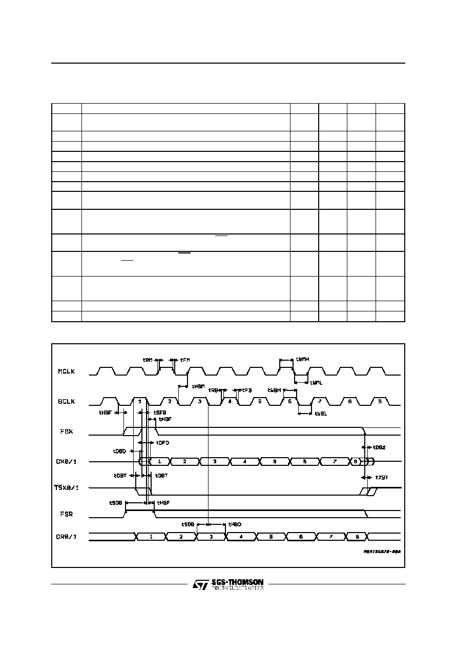
Figure 5: Non Delayed Data Timing (short frame mode)
TS5070 - TS5071
19/32
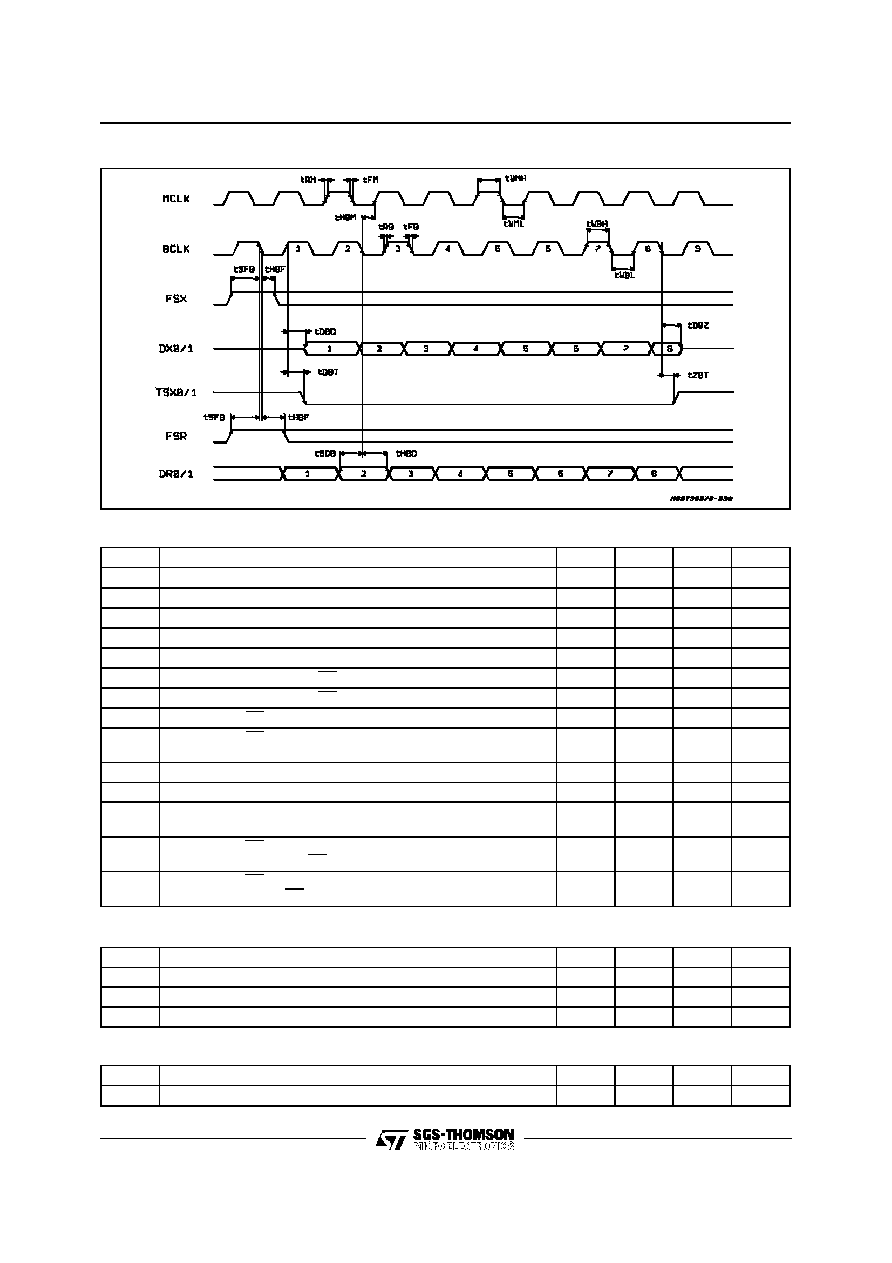
Figure 6: Delayed Data Timing (short frame mode)
SERIAL CONTROL PORT TIMING
Symbol
Parameter
Min.
Typ.
Max.
Unit
f
CCLK
Frequency of CCLK
2.048
MHz
t
WCH
Period of CCLK High (measured from V
IH
to V
IH
)
160
ns
t
WCL
Period of CCLK Low (measured from V
IL
to V
IL
)
160
ns
t
RC
Rise Time of CCLK (measured from V
IL
to V
IH
)
50
ns
t
FC
Fall Time of CCLK (measured from V
IH
to V
IL
)
50
ns
t
HCS
Hold Time, CCLK Low to CS Low (CCLK1)
10
ns
t
HSC
Hold Time, CCLK Low to CS High (CCLK8)
100
ns
t
SSC
Setup Time, CS Transition to CCLK Low
70
ns
t
SSCO
Setup Time, CS Transition to CCLK High (to insure CO is not
enabled for single byte)
50
ns
t
SDC
Setup Time, CI (CI/O) Data in to CCLK low
50
ns
t
HCD
Hold Time, CCLK Low to CI (CI/O) Invalid
50
ns
t
DCD
Delay Time, CCLK High to CO (CI/O) Data Out Valid
(load = 100 pF plus 2 LSTTL loads)
80
ns
t
DSD
Delay Time, CS Low to CO (CI/O) Valid
(applies only if separate CS used for byte 2)
80
ns
t
DDZ
Delay Time, CS or CCLK9 High to CO (CI/O) High Impedance
(applies to earlier of CS high or CCLK9 high)
15
80
ns
INTERFACE LATCH TIMING
Symbol
Parameter
Min.
Typ.
Max.
Unit
t
SLC
Setup Time, I
L
Valid to CCLK 8 of Byte 1 Low. I
L
as Input
100
ns
t
HCL
Hold Time, I
L
Valid from CCLK 8 of Byte 1 Low. I
L
as Input
50
ns
t
DCL
Delay Time, CCLK 8 of Byte 2 Low to I
L
. C
L
= 50 pF. I
L
as Output
200
ns
MASTER RESET PIN
Symbol
Parameter
Min.
Typ.
Max.
Unit
t
WMR
Duration of Master Reset High
1
µ
s
TS5070 - TS5071
20/32
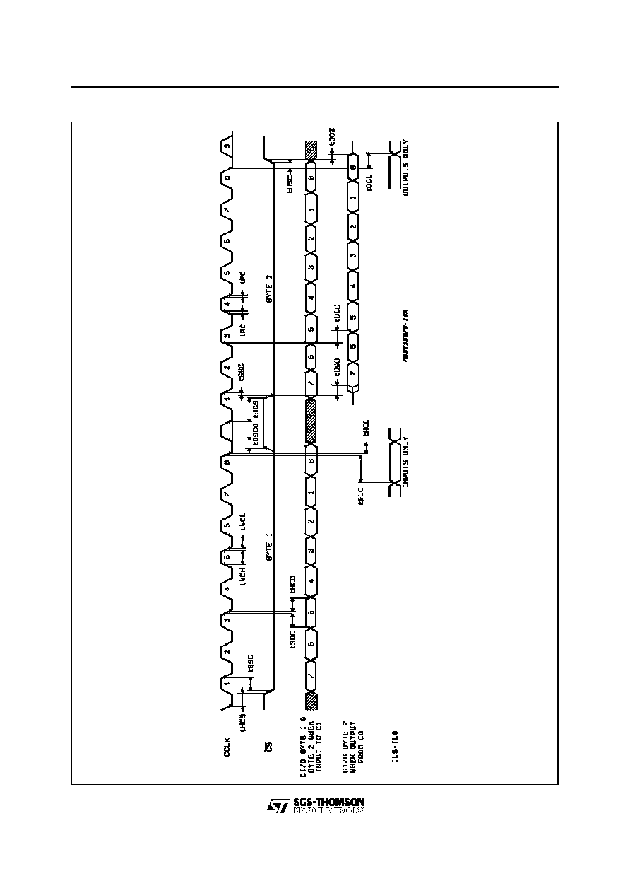
Figure 7: Control Port Timing
TS5070 - TS5071
21/32
TRANSMISSION CHARACTERISTICS
Unless otherwise noted, limits printed in BOLD
characters are guaranteed for V
CC
= + 5 V
±
5 % ;
V
SS
= ≠ 5 V
±
5 %, T
A
=-40
∞
C to 85
∞
C by correlation
with 100 % electrical testing at T
A
= 25
∞
C (-40
∞
C
to 85
∞
C for TS5070-X and TS5071-X).
f = 1031.25 Hz, VF
X
I = 0 dBm0, D
R
0 or D
R
1 = 0
dBm0 PCM code, Hybrid Balance filter disabled. All
other limits are assured by correlation with other
production tests and/or product design and char-
acterization. All signals referenced to GND. dBm
levels are into 600 ohms. Typicals specified at
V
CC
= + 5 V, V
SS
= -5 V, T
A
= 25
∞
C.
AMPLITUDE RESPONSE
Symbol
Parameter
Min.
Typ.
Max.
Unit
Absolute levels
The nominal 0 dBm 0 levels are :
VF
X
I
0 dB Tx Gain
25.4 dB Tx Gain
VF
R
O
0 dB Rx Attenuation (RL
15 k
)
0.5 dB Rx Attenuation (RL
600
)
1.2 dB Rx Attenuation (RL
300
)
25.4 dB Rx Attenuation
1.618
86.9
1.968
1.858
1.714
105.7
Vrms
mVrms
Vrms
Vrms
Vrms
mVrms
Maximum Overload
The nominal overload levels are :
A-law
VF
X
I
0 dB Tx Gain
25.4 dB Tx Gain
VF
R
O
0 dB Rx Attenuation (R
L
15 k
)
0.5 dB Rx Attenuation (R
L
300
)
1.2 dB Rx Attenuation (R
L
300
)
25.4 dB Rx Attenuation
µ
-law
VF
X
I
0 dB Tx Gain
25.4 dB Tx Gain
VF
R
O
0 dB Rx Attenuation (R
L
15 k
)
0.5 dB Rx Attenuation (R
L
600
)
1.2 dB Rx Attenuation (R
L
300
)
25.4 dB Rx Attenuation
2.323
124.8
2.825
2.667
2.461
151.7
2.332
125.2
2.836
2.677
2.470
152.3
Vrms
mVrms
Vrms
Vrms
Vrms
mVrms
Vrms
mVrms
Vrms
Vrms
Vrms
mVrms
GXA
Transmit Gain Absolute Accurary
Transmit Gain Programmed for 0 dBm0 = 6.4 dBm, A-law
Measure Deviation of Digital Code from Ideal 0 dBm0 PCM Code
at D
X
0/1, f = 1031.25 Hz
T
A
= 25
∞
C, V
CC
= 5 V, V
SS
= ≠ 5 V
≠ 0.15
0.15
dB
GXAG
Transmit gain Variation with Programmed Gain
Programmed level from
-12.6dBm
0dBm
6.4dBm
Programmed level from
-19dBm
0dBm
12.7dBm
Note:
±
0.1dB min/max is available as a selected part
Calculate the Deviation from the Programmed Gain Relative to
GXA
i.e., GXAG = Gactual ≠ Gprog ≠ GXA
T
A
= 25
∞
C, V
CC
= 5 V, V
SS
= ≠ 5 V
≠ 0.1
≠ 0.3
0.1
0.3
dB
dB
TS5070 - TS5071
22/32
AMPLITUDE RESPONSE (continued)
Symbol
Parameter
Min.
Typ.
Max.
Unit
GXAF
Transmit Gain Variation with Frequency
Relative to 1031.25 Hz (note 2)
-19 dBm < o dBm0 < 6.4 dBm
D
R
0 (or D
R
1) = 0 dBm0 Code
f = 60Hz
f = 200 Hz
f = 300 Hz to 3000 Hz
f = 3400 Hz
f = 4000 Hz
f > 4600 Hz Measure Response at Alias Frequency from 0 kHz to 4 kHz
0 dBm0 = 6.4 dBm
VFXI = -4 dBm0 (note2)
f = 62.5 Hz
f = 203.125 Hz
f = 2093.750 Hz
f = 2984.375 Hz
f = 3296.875 Hz
f = 3406.250 Hz
f = 3984.375 Hz
f = 5250 Hz, Measure 2750 Hz
f = 11750Hz, Measure 3750 Hz
f = 49750 Hz, Measure 1750 Hz
-1.8
-0.15
-0.7
-1.7
-0.15
-0.15
-0.15
-0.74
-26
-0.1
0.15
0
-14
-32
dB
dB
dB
dB
dB
dB
dB
dB
dB
dB
dB
dB
dB
dB
dB
dB
GXAT
Transmit Gain Variation with Temperature
Measured Relative to GXA, VCC = 5V, VSS= -5V -19dBm < 0dBm < 6.4dBm
-0.1
0.1
dB
GXAV
Transmit Gain Variation with Supp ly
V
CC
= 5V
±
5%, V
SS
= -5V
±
5%
Measured Relative to GXA
T
A
= 25
∞
C, o dBm0 = 6.4dBm
-0.05
0.05
dB
GXAL
Transmit Gain Variation with Signal Level
Sinusoidal Test Method, Reference Level = 0 dBm0
VF
X
I = -40 dBm0 to + 3 dBm0
VF
X
I = -50 dBm0 to -40 dBm0
VF
X
I = -55 dBm0 to -50 dBm0
-0.2
-0.4
-1.2
0.2
0.4
1.2
dB
dB
dB
GRA
Receive Gain Absolute Accuracy
0 dBm0 = 8.1 dBm, A-law
Apply 0 dBm0 PCM Code to D
R
0 or D
R
1 Measure VF
R
O, f =1015.625Hz
T
A
= 25
∞
C, V
CC
= 5V, V
SS
= -5V
-0.15
0.15
dB
GRAG
Receive Gain Variation with Programmed Gain
Programmed level from
-10.9dBm
0dBm
8.1dBm
Programmed level from
-17.3dBm
0dBm
-11dBm
Note:
±
0.1dB min/max is available as a selected part
Calculate the Deviation from the Programmed Gain Relative to GRA
I.e. GRAG = Gactual - Gprog - GRA T
A
= 25
∞
C, V
CC
= 5V, V
SS
= -5V
-0.1
-0.3
0.1
0.3
dB
dB
-24.9
-0.1
0.15
0.15
0.15
0
-13.5
-32
-32
-32
TS5070 - TS5071
23/32
AMPLITUDE RESPONSE (continued)
Symbol
Parameter
Min.
Typ.
Max.
Unit
GRAT
Receive Gain Variation with Temperature
Measure Relative to GRA
V
CC
= 5V, V
SS
= -5V -17dBm < 0dBm0 < 8.1dBm
-0.1
0.1
dB
GRAV
Receive Gain Variation with Supply
Measured Relative to GRA
V
CC
= 5V
±
5%, V
SS
= -5V
±
5%
T
A
= 25
∞
C, 0dBm 0 = 8.1 dBm
-0.05
0.05
dB
GRAF
Receive Gain Variation with Frequency
Relative to 1015.625 Hz, (note 2)
D
R
0 or D
R
1 = 0 dBm0 Code
-17.3dBm < 0 dBm0 < 8.1dBm
f = 200Hz
f = 300Hz to 3000Hz
f = 3400Hz
f = 4000Hz
GR = 0dBm0 = 8.1dBm
D
R
0 = -4dBm0
Relative to 1015.625 (note 2)
f = 296.875 Hz
f = 1906.250Hz
f = 2812.500Hz
f = 2984.375Hz
f = 3406.250Hz
f = 3984.375Hz
-0.25
-0.15
-0.7
-0.15
-0.15
-0.15
-0.15
-0.74
0.15
0.15
0
-14
0.15
0.15
0.15
0.15
0
-13.5
dB
dB
dB
dB
dB
dB
dB
dB
dB
dB
GRAL
Receive Gain Variation with Signal Level
Sinusoidal Test Method Reference Level = 0dBm0
D
R
0 = -40dBm0 to +3dBm0
D
R
0 = -50dBm0 to -40dBm0
D
R
0 = -55dBm0 to -50dBm0
DR0 = 3.1dBm0
R
L
= 600
, 0dBm0 = 7.6dBm
R
L
= 300
, 0dBm0 = 6.9dBm
-0.2
-0.4
-1.2
-0.2
-0.2
0.2
0.4
1.2
0.2
0.2
dB
dB
dB
dB
dB
TS5070 - TS5071
24/32

ENVELOPE DELAY DISTORTION WITH FREQUENCY
Symbol
Parameter
Min.
Typ.
Max.
Unit
DXA
Tx Delay Absolute
f = 1600 Hz
315
µ
s
DXR
Tx Delay, Relative to DXA
f = 500 ≠ 600 Hz
f = 600 ≠ 800 Hz
f = 800 ≠ 1000 Hz
f = 1000 ≠ 1600 Hz
f = 1600 ≠ 2600 Hz
f = 2600 ≠ 2800 Hz
f = 2800 ≠ 3000 Hz
220
145
75
40
75
105
155
µ
s
µ
s
µ
s
µ
s
µ
s
µ
s
µ
s
DRA
Rx Delay, Absolute
f = 1600 Hz
200
µ
s
DRR
Rx Delay, Relative to DRA
f = 500 ≠ 1000 Hz
f = 1000 ≠ 1600 Hz
f = 1600 ≠ 2600 Hz
f = 2600 ≠ 2800 Hz
f = 2800 ≠ 3000 Hz
≠ 40
≠ 30
90
125
175
µ
s
µ
s
µ
s
µ
s
µ
s
TS5070 - TS5071
25/32

NOISE
Symbol
Parameter
Min.
Typ.
Max.
Unit
NXC
Transmit Noise, C Message Weighted
µ
-law Selected (note 3)
0 dBm0 = 6.4dBm
12
15
dBrnC0
NXP
Transmit Noise, Psophometric Weighted
A-law Selected (note 3)
0 dBm0 = 6.4dBm
-74
-67
dBm0p
NRC
Receive Noise, C Message Weighted
µ
-law Selected
PCM code is alternating positive and negative zero
8
11
dBrnC0
NRP
Receive Noise, Psophometric Weighted
A-law Selected
PCM Code Equals Positive Zero
-82
-79
dBm0p
NRS
Noise, Single Frequency
f = 0Hz to 100kHz, Loop Around Measurement VF
X
I = 0Vrms
-53
dBm0
PPSRX
Positive Power Supply Rejection Transmit
V
CC
= 5V
DC
+ 100mVrms
f = 0Hz to 4000Hz (note 4)
f = 4kHz to 50kHz
30
30
dBp
dBp
NPSRX
Negative Power Supply Rejection Transmit
V
SS
= -5V
DC
+ 100mVrms
f = 0Hz to 4000Hz (note 4)
f = 4kHz to 50kHz
30
30
dBp
dBp
PPSRR
Positive Power Supply Rejection Receive
PCM Code Equals Positive Zero
V
CC
= 5V
DC
+ 100mVrms
Measure VFR0
f = 0Hz to 4000Hz
f = 4kHz to 25kHz
f = 25kHz to 50kHz
30
40
36
dBp
dB
dB
NPSRR
Negative Power Supply Rejection Receive
PCM Code Equals Positive Zero
V
SS
= -5V
DC
+ 100mVrms
Measure VFR0
f = 0Hz to 4000Hz
f = 4kHz to 25kHz
f = 25kHz to 50kHz
30
40
36
dBp
dB
dB
SOS
Spurious Out-of Band Signals at the Channel Output
0dBm0 300Hz to 3400Hz input PCM code applied at D
R
0 (D
R
1)
Relative to f = 1062.5Hz
4600Hz to 7600Hz
7600Hz to 8400Hz
8400Hz to 50000Hz
-30
-40
-30
dB
dB
dB
TS5070 - TS5071
26/32
DISTORTION
Symbol
Parameter
Min.
Typ.
Max.
Unit
STDX
Signal to Total Distortion Transmit
Sinusoidal Test Method
Half Channel
Level = 3dBm0
Level = -30dBm0 to 0dBm0
Level = -40dBm0
Level = -45dBm0
33
36
30
25
dBp
dBp
dBp
dBp
STDR
Signal to Total Distortion Receive
Sinusoidal Test Method
Half Channel
Level = 3dBm0
Level = -30dBm0 to 0dBm0
Level = -40dBm0
Level = -45dBm0
33
36
30
25
dBp
dBp
dBp
dBp
SFDX
Single Frequency Distortion Transmit
-46
dB
SFDR
Single Frequency Distortion Receive
-46
dB
IMD
Intermodulation Distortion Transmit or Receive
Two Frequencies in the Range 300Hz to 3400Hz
-41
dB
CROSSTALK
Symbol
Parameter
Min.
Typ.
Max.
Unit
CTX-R
Transmit to Receive Crosstalk,
0dBm0 Transmit Level
f = 300 to 3400Hz
DR = Idle PCM Code
-90
-75
dB
CTR-X
Receive to Transmit Crosstalk,
0dBm0 Receive Level
f = 300 to 3400Hz (note 4)
-90
-70
dB
Notes:
1. Applies only to MCLK frequencies
1.536 MHz. At 512 kHz A 50:50
±
2 % duty cycle must be used.
2. A multi-tone test technique is used (peak/rms
9.5 dB).
3. Measured by grounded input at VF
X
I.
4. PPSRX, NPSRX and CTR-X are measured with a ≠ 50 dBm0 activation signal applied to VF
X
I.
A signal is Valid if it is above V
IH
or below V
IL
and invalid if it is between V
IL
and V
IH
. For the purpose of the specification the following conditions
apply :
a) All input signals are defined as V
IL
= 0.4 V, V
IH
= 2.7 V, t
R
< 10 ns, t
F
10 ns
b) t
R
is measured from V
IL
to V
IH
, t
F
is measured from V
IH
to V
IL
c) Delay Times are measured from the input signal Valid to the clock input invalid
d) Setup Times are measured from the data input Valid to the clock input invalid
e) Hold Times are measured from the clock signal Valid to the data input invalid
f) Pulse widths are measured from V
IL
to V
IL
or from V
IH
to V
IH
TS5070 - TS5071
27/32

DEFINITIONS AND TIMING CONVENTIONS
DEFINITIONS
V
IH
VIH is the D.C. input level above which an input level is guaranteed to appear as a logical one.
This parameter is to be measured by performing a functional test at reduced clock speeds and
nominal timing (i.e. not minimum setup and hold times or output strobes), with the high level of
all driving signals set to V
IH
and maximum supply voltages applied to the device.
V
IL
VIL is the D.C. input level below which an input level is guaranteed to appear as a logical zero
the device. This parameter is measured in the same manner as V
IH
but with all driving signal
low levels set to V
IL
and minimum supply voltage applied to the device.
V
OH
VOH is the minimmum D.C. output level to which an output placed in a logical one state will
converge when loaded at the maximum specified load current.
V
OL
VOL is the maximum D.C. output level to which an output placed in a logical zero state will
converge when loaded at the maximum specified load current.
Threshold Region
Valid Signal
The threshold region is the range of input voltages between V
IL
and V
IH
.
A signal is Valid if it is in one of the valid logic states. (i.e. above V
IH
or below V
IL
). In timing
specifications, a signal is deemed valid at the instant it enters a valid state.
Invalid signal
A signal is invalid if it is not in a valid logic state, i.e., when it is in the threshold region between
V
IL
and V
IH
. In timing specifications, a signal is deemed Invalid at the instant it enters the
threshold region.
TIMING CONVENTIONS
For the purpose of this timing specifications the following conventions apply :
Input Signals
All input signals may be characterized as : V
L
= 0.4 V, V
H
= 2.4 V, tR < 10 ns, tF < 10 ns.
Period
The period of the clock signal is designated as tPxx where xx represents the mnemonic of the
clock signal being specified.
Rise Time
Rise times are designated as tRyy, where yy represents a mnemonic of the signal whose rise
time is being specified, tRyy is measured from V
IL
to V
IH
.
Fall Time
Fall times are designated as tFyy, where yy represents a mnemonic of the signal whose fall
time is being specified, tFyy is measured from V
IH
to V
IL
.
Pulse Width High
The high pulse width is designated as tWzzH, where zz represents the mnemonic of the input
or output signal whose pulse width is being specified. High pulse width are measured from V
IH
to V
IH
.
Pulse Width Low
The low pulse is designated as tWzzL' where zz represents the mnemonic of the input or output
signal whose pulse width is being specified. Low pulse width are measured from V
IL
to V
IL
.
Setup Time
Setup times are designated as tSwwxx where ww represents the mnemonic of the input signal
whose setup time is being specified relative to a clock or strobe input represented by mnemonic
xx. Setup times are measured from the ww Valid to xx Invalid.
Hold Time
Hold times are designated as THwwxx where ww represents the mnemonic of the input signal
whose hold time is being specified relative to a clock or strobe input represented by the
mnemonic xx. Hold times are measured from xx Valid to ww Invalid
Delay Time
Delay times are designated as TDxxyy [H/L], where xx represents the mnemonic of the input
reference signal and yy represents the mnemonic of the output signal whose timing is being
specified relative to xx. The mnemonic may optionally be terminated by an H or L to specify the
high going or low going transition of the output signal. Maximum delay times are measured from
xx Valid to yy Valid. Minimum delay times are measured from xx Valid to yy Invalid. This
parameter is tested under the load conditions specified in the Conditions column of the Timing
Specifications section of this datasheet.
TS5070 - TS5071
28/32
COMBO II SALES TYPE LIST
Ordering
Number
Electrical
description
Package Marking Packing
TS5070FN
Stdandard
Selection
Datasheet
December
1997
PLCC28 TS5070FN Tubes
TS5070FNTR
PLCC28 TS5070FN
Tape
and reel
TS5071N
PDIP20 TS5071N
Tubes
TSW5070FN
Relaxed
selection
(Gxa, Gra,
Grag, Gxag)
PLCC28 TS5070FN Tubes
Param Page
Conditions
Min Max Unit
TSW5070FNTR
PLCC28 TS5070FN
Tape
and reel
Gxa
22
--
-0.2 0.2
dB
TSW5071N
PDIP20 TS5071N
Tubes
Gxag
22
-6.3dBm<0dbm0<6.4dBm
-0.1 0.1
dB
-12.7dBm<0dBm0<-6.4dBm -0.2 0.2
dB
-19dBm<0dBm0<-12.8dBm
-0.5 0.5
dB
Gra
23
--
-0.2 0.2
dB
Grag
23
-4.6dBm<0dBm0<8.1dBm
-0.1 0.1
dB
-11dBm<0dBm0<-4.7dBm
-0.2 0.2
dB
-17.3dBm<0dBm0<-11.1dBm -0.5 0.5
dB
TSP5070FN
Special
selection
for
Grag/Gxag
PLCC28 TS5070FN
Tubes
Param Page
Conditions
Min Max Unit
TSP5070FNTR
PLCC28 TS5070FN
Tape
and reel
Gxag
22
all programmed gains
-0.1 0.1
dB
TSP5071N
PDIP20 TS5071N
Tubes
Grag
23
all programmed gains
-0.1 0.1
dB
TS5070 - TS5071
29/32
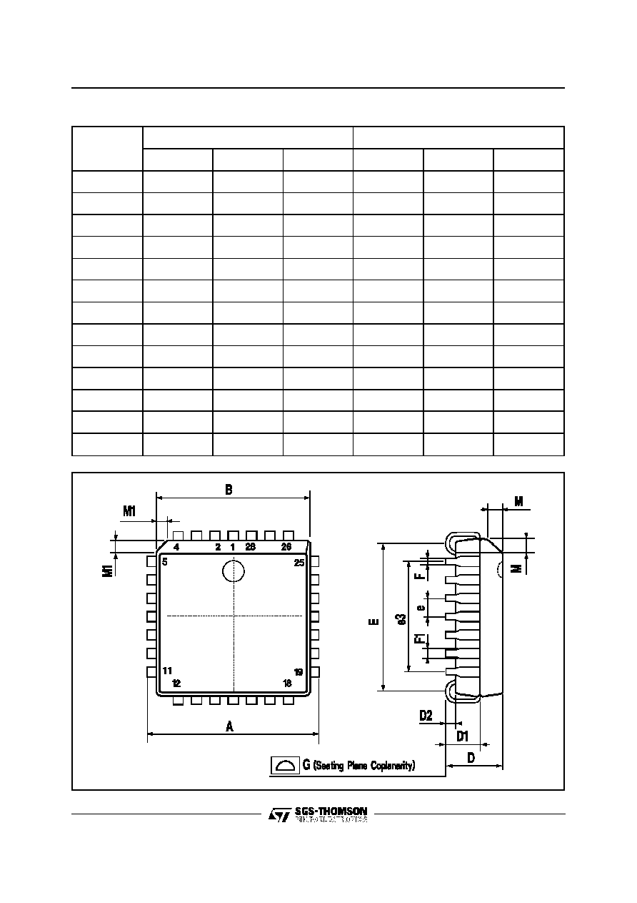
PLCC28 PACKAGE MECHANICAL DATA
DIM.
mm
inch
MIN.
TYP.
MAX.
MIN.
TYP.
MAX.
A
12.32
12.57
0.485
0.495
B
11.43
11.58
0.450
0.456
D
4.2
4.57
0.165
0.180
D1
2.29
3.04
0.090
0.120
D2
0.51
0.020
E
9.91
10.92
0.390
0.430
e
1.27
0.050
e3
7.62
0.300
F
0.46
0.018
F1
0.71
0.028
G
0.101
0.004
M
1.24
0.049
M1
1.143
0.045
TS5070 - TS5071
30/32
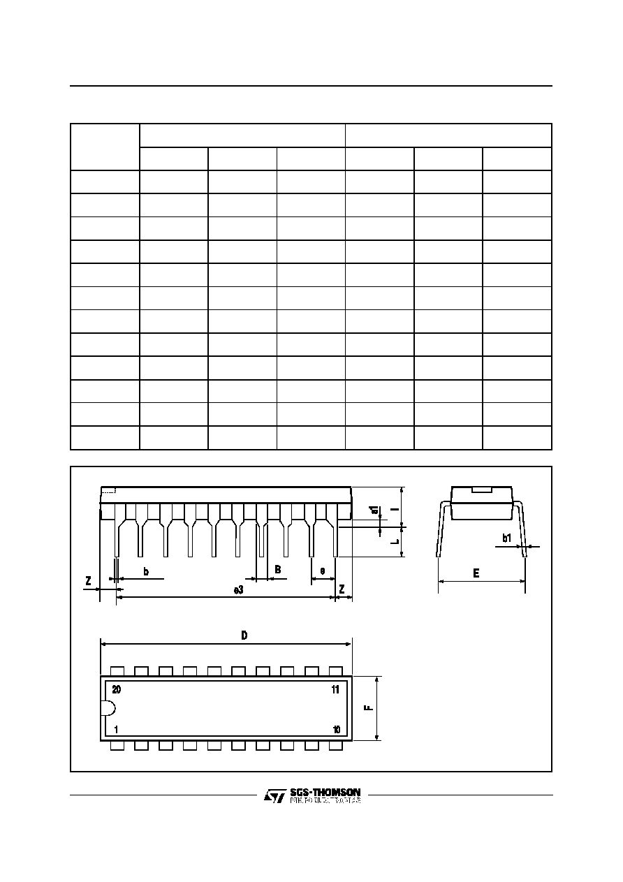
DIP20 PACKAGE MECHANICAL DATA
DIM.
mm
inch
MIN.
TYP.
MAX.
MIN.
TYP.
MAX.
a1
0.254
0.010
B
1.39
1.65
0.055
0.065
b
0.45
0.018
b1
0.25
0.010
D
25.4
1.000
E
8.5
0.335
e
2.54
0.100
e3
22.86
0.900
F
7.1
0.280
I
3.93
0.155
L
3.3
0.130
Z
1.34
0.053
TS5070 - TS5071
31/32

Information furnished is believed to be accurate and reliable. However, SGS-THOMSON Microelectronics assumes no responsibility for the
consequences of use of such information nor for any infringement of patents or other rights of third parties which may result from its use. No
license is granted by implication or otherwise under any patent or patent rights of SGS-THOMSON Microelectronics. Specification mentioned
in this publication are subject to change without notice. This publication supersedes and replaces all information previously supplied. SGS-
THOMSON Microelectronics products are not authorized for use as critical components in life support devices or systems without express
written approval of SGS-THOMSON Microelectronics.
©
1997 SGS-THOMSON Microelectronics ≠ Printed in Italy ≠ All Rights Reserved
SGS-THOMSON Microelectronics GROUP OF COMPANIES
Australia - Brazil - Canada - China - France - Germany - Italy - Japan - Korea - Malaysia - Malta - Morocco - The Netherlands -
Singapore - Spain - Sweden - Switzerland - Taiwan - Thailand - United Kingdom - U.S.A.
TS5070 - TS5071
32/32