 | –≠–ª–µ–∫—Ç—Ä–æ–Ω–Ω—ã–π –∫–æ–º–ø–æ–Ω–µ–Ω—Ç: TSM104N | –°–∫–∞—á–∞—Ç—å:  PDF PDF  ZIP ZIP |
Æ
N
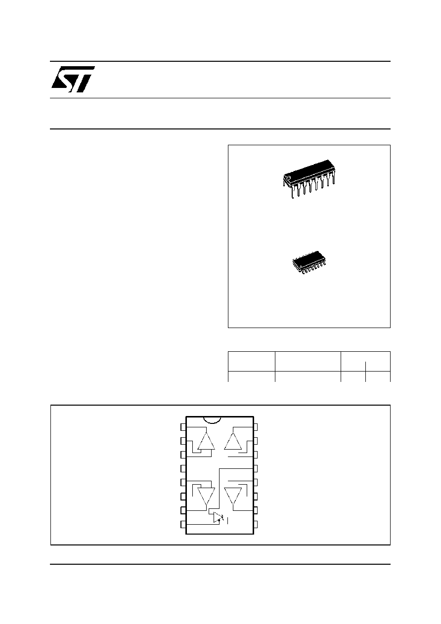
DIP16
(Plastic Package)
OPERATIONAL AMPLIFIERS
.
LOW SUPPLY CURRENT : 375
µ
A/op.
(@ V
CC
= 5V)
.
LOW INPUT BIAS CURRENT : 20nA
.
MEDIUM SPEED : 0.9MHz
.
LOW INPUT OFFSET VOLTAGE : 0.5mV typ
for TSM104A
.
WIDE POWER SUPPLY RANGE :
±
1.5V to
±
15V
VOLTAGE REFERENCE
.
ADJUSTABLE OUTPUT VOLTAGE :
V
ref
to 36V
.
0.4% AND 1% VOLTAGE PRECISION
.
SINK CURRENT CAPABILITY : 1 to 100mA
.
TYPICAL OUTPUT IMPEDANCE : 0.2
DESCRIPTION
The TSM104 is a monolithic IC that includes four
op-amps and an adjustable shunt voltage refer-
ence. This device is offering space and cost saving
in many applications like power supply manage-
ment or data acquisition systems.
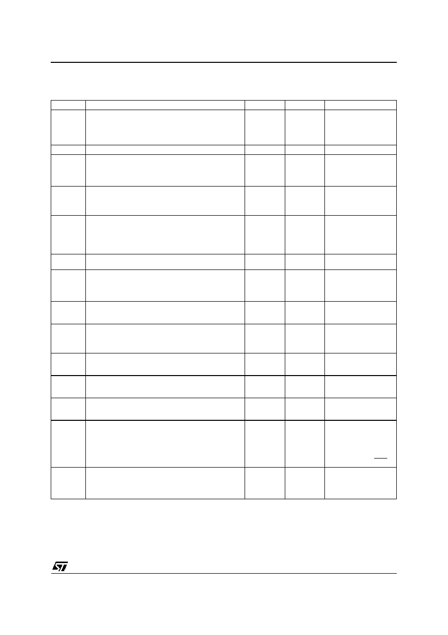
1
2
3
4
13
14
15
16
5
6
7
8
12
11
10
9
Output 1
Inverting Input 1
Non-inve rting Input 1
V
CC
+
Non-inve rting Input 2
Inverting Input 2
Output 2
Adjust
Output 4
Inverting Input
Non-inve rting Input 4
Non-inve rting Input 3
Inverting Input 3
Output 3
Ca thode
V
CC
-
PIN CONNECTIONS
QUAD OPERATIONAL AMPLIFIER AND
PROGRAMMABLE VOLTAGE REFERENCE
TSM104/A
ORDER CODES
Part number
Temperature Range
Package
N
D
TSM104I/AI
-40
o
C, +105
o
C
∑
∑
February1999
D
SO16
(Plastic Micropac
1/9

ABSOLUTE MAXIMUM RATINGS
Symbol
Parameter
Value
Unit
V
CC
Supply Voltage
36
V
V
id
Differential Input Voltage
36
V
V
i
Input Voltage
-0.3 to 36
V
T
oper
Operating Free-air Temperature Range
-55 to +125
o
C
T
j
Maximum Junction Temperature
150
o
C
R
thja
Thermal Resistance Juction to Ambient (SO package)
150
o
C/W
ELECTRICAL CHARACTERISTICS
V
CC
+
= 5V, V
CC
-
= 0V, T
amb
= 25
o
C (unless otherwise specified)
Symbol
Parameter
Min
Typ
Max
Unit
I
CC
Total Supply Current, excluding current in the
Voltage Reference
V
CC
+
= 5V, no load
T
min.
< T
amb
< T
max
V
CC
+
= 30V, no load
T
min.
< T
amb
< T
max
1.4
2.4
4
mA
TSM104/A
2/9
OPERATIONAL AMPLIFIERS
V
CC
+
= 5V, V
CC
-
= Ground, V
O
= 1.4V, T
amb
= 25
o
C (unless otherwise specified)
Symbol
Parameter
Min.
Typ.
Max.
Unit
V
io
Input Offset Voltage
TSM104, T
amb
= 25
o
C
T
min.
T
amb
T
max.
TSM104A, T
amb
= 25
o
C
T
min.
T
amb
T
max.
1
0.5
5
6
3
4
mV
DV
io
Input Offset Voltage Drift
7
µ
V/
o
C
I
io
Input Offset Current
T
min.
T
amb
T
max.
2
30
50
nA
I
ib
Input Bias Current
T
min.
T
amb
T
max.
20
150
200
nA
A
vd
Large Signal Voltage Gain
V
CC
= 15V, R
L
= 2k
V
O
= 1.4V to 11.4V
T
min.
T
amb
T
max.
50
25
100
V/mV
SVR
Supply Voltage Rejection Ratio
V
CC
= 5V to 30V
65
100
dB
V
icm
Input Voltage Mode Voltage Range
V
CC
= +30V - see note 1
T
min.
T
amb
T
max.
0
0
VCC
+
-1.5
V
CC
+
-2
V
CMR
Common Mode Rejection Ratio
T
min.
T
amb
T
max.
70
60
85
dB
I
source
Output Current Source
V
o
= 2V, V
CC
= +15V, V
id
= +1V
20
40
mA
I
O
Short Circuit to Ground
V
CC
= +15V
40
60
mA
I
sink
Output Current Sink
V
id
= -1V,
V
CC
= +15V, V
o
= +2V
10
20
mA
V
OH
High Level Output Voltage
R
L
= 10k, V
CC
+
= 30V
T
amb
= 25
o
C
T
min.
T
amb
T
max.
27
27
28
V
V
OL
Low Level Output Voltage
R
L
= 10k
T
min.
T
amb
T
max.
5
20
20
mV
SR
Slew Rate at Unity Gain
V
i
= 0.5 to 3V, V
CC
= 15V
R
L
= 2k, C
L
= 100pF, unity gain
0.1
0.3
V/
µ
s
GBP
Gain Bandwidth Product
V
CC
= 30V, R
L
= 2k, C
L
= 100pF
f = 100kHz, V
in
= 10mV
0.5
0.9
MHz
THD
Total Harmonic Distortion
f = 1kHz
A
V
= 20dB, R
L
= 2k, V
CC
= 30V
C
L
= 100pF, V
O
= 2V
pp
0.02
%
en
Equivalent Input Noise Voltage
f = 1kHz, V
CC
= 30V, R
S
= 100
50
nV
Hz
cs
Channel Separation
1kHz < f < 20kHz
120
dB
C
s
Channel Separation
1kHz<f<20kHz
120
dB
Note 1 :
The input common-mode voltage of either input signal voltage should not be allowed to go negative by more than 0.3V. The upper
end of the common-mode voltage range is V
CC
+
-1.5V
But either of both inputs can go to +36V without damage.
TSM104/A
3/9
VOLTAGE REFERENCE
Symbol
Parameter
Value
Unit
I
K
Cathode Current
1 to 100
mA
Symbol
Parameter
Min.
Typ.
Max.
Unit
V
ref
Reference Input Voltage
TSM104, T
amb
= 25
o
C
T
min.
T
amb
T
max.
TSM104A, T
amb
= 25
o
C
T
min.
T
amb
T
max.
2.475
2.45
2.49
2.48
2.5
2.5
2.525
2.55
2.51
2.52
V
V
ref
Reference Input Voltage Deviation Over
Temperature Range
V
KA
= V
ref,
I
K =
10mA
T
min.
T
amb
T
max.
7
30
mV
V
ref
V
KA
Ratio of Change in Reference Input Voltage to Change in Cathode to
Anode Voltage
I
K
= 10mA,
V
ka
= 36V to 3V
-2
-1.1
mV/V
I
ref
Reference Input Current
I
K
= 10mA
T
min.
T
amb
T
max.
1.5
2.5
3
µ
A
I
ref
Reference Input Current Deviation over T
o
Range
0.8
1.2
µ
A
I
min
Minimum Cathode Current for Regulation
V
KA
= V
ref
0.5
1
mA
I
off
Off-State Cathode Current
180
500
nA
|Z
KA
|
Dynamic Impedance - (note 1)
V
KA
= V
ref
,
I
K
= 1 to 100mA, f < 1kHz
0.2
0.5
Note 1 : the dynamic impedance is defined as |Z
KA
| =
V
KA
/
I
K
TSM104/A
4/9

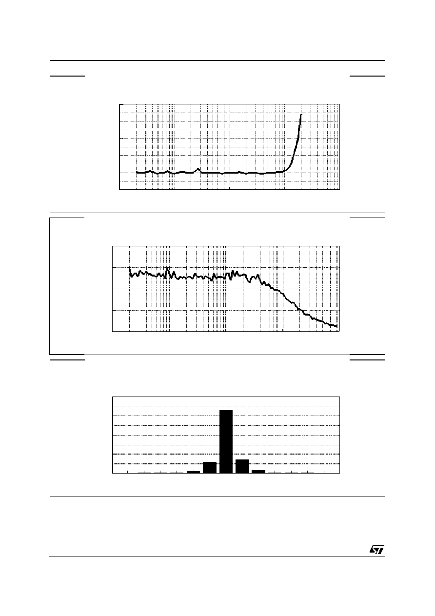
-0,015
-0,01
-0,005
0
0,005
0,01
0,015
0
200
400
600
800
1000
Thousands
source <=
I (A)
=> sink
Unit
Freq
Unit Frequency = F(I)
Vcc=+/-15V, RL=2k, CL=100pF
-0,015
-0,01
-0,005
0
0,005
0,01
0,015
0
10
20
30
40
50
60
-14
-12
-10
-8
-6
-4
-2
0
2
Gain
Margin
(dB)
source <=
I (A)
=> sink
Phase
Margin
(deg)
Phase and Gain Margin = F(I)
Vcc=+/- 15V, RL=2k, CL=100pF
-0,015
-0,01
-0,005
0
0,005
0,01
0,015
0
200
400
600
800
Thousands
source <=
I (A)
=> sink
GBP
GBP = F(I)
Vcc=+/-15V, RL=2k, CL=100pF
OPERATIONAL AMPLIFIERS
TSM104/A
5/9
0,01
0,1
1
10
100
0
20
40
60
80
Frequency (Hz)
Noise(nV/SQR(Hz))
Noise = F(frequency)
10
100
1000
10000
100000
0,004
0,006
0,008
0,01
0,012
0,014
Frequency (Hz)
THD(%)
Total Harmonic Distorsion THD = F(freq)
0
20
40
60
80
Vio (mV)
Distribution
(%)
-3
-2,5
-2
-1,5
-1
-0,5
0
0,5
1
1,5
2
2,5
3
Vio Distribution
Vcc+=5V, Vcc-=0V
TSM104/A
6/9

0,0001
0,001
0,01
0,1
0,5
1
1,5
2
2,5
3
Cathode Curr ent Ik (Amps)
Vref
(V)
Vref = F(Ik)
1,000000E-10
1,000000E-09
1,000000E-08
1,000000E-07
1,000000E-06
0,00001
0
0,02
0,04
0,06
Capacitor(F)
Current
(Amps)
Vref Stability = f(I,C)
Unstable
Stable
VOLTAGE REFERENCE
TSM104/A
7/9
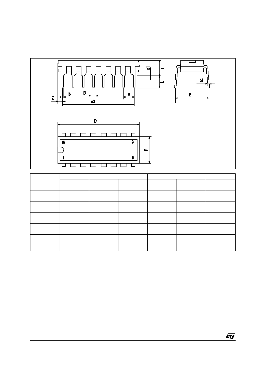
PACKAGE MECHANICAL DATA
16 PINS - PLASTIC PACKAGE
Dim.
Millimeters
Inches
Min.
Typ.
Max.
Min.
Typ.
Max.
a1
0.51
0.020
B
0.77
1.65
0.030
0.065
b
0.5
0.020
b1
0.25
0.010
D
20
0.787
E
8.5
0.335
e
2.54
0.100
e3
17.78
0.700
F
7.1
0.280
i
5.1
0.201
L
3.3
0.130
Z
1.27
0.050
TSM104/A
8/9
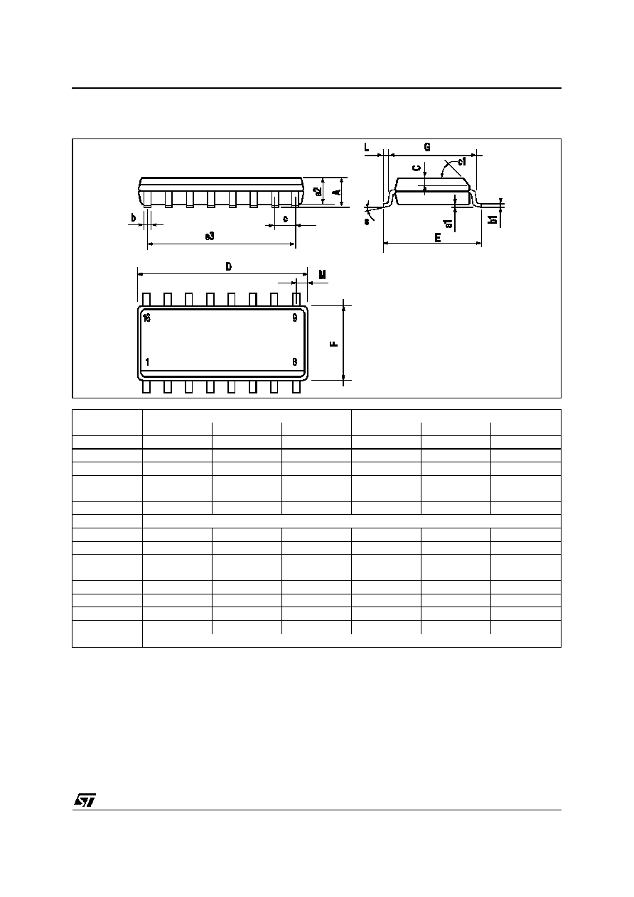
PACKAGE MECHANICAL DATA
16 PINS - PLASTIC MICROPACKAGE (SO)
Dim.
Millimeters
Inches
Min.
Typ.
Max.
Min.
Typ.
Max.
A
1.75
0.069
a1
0.1
0.2
0.004
0.008
a2
1.6
0.063
b
0.35
0.46
0.014
0.018
b1
0.19
0.25
0.007
0.010
C
0.5
0.020
c1
45
o
(typ.)
D
9.8
10
0.386
0.394
E
5.8
6.2
0.228
0.244
e
1.27
0.050
e3
8.89
0.350
F
3.8
4.0
0.150
0.157
G
4.6
5.3
0.181
0.209
L
0.5
1.27
0.020
0.050
M
0.62
0.024
S
8
o
(max.)
Information furnished is believed to be accurate and reliable. However, STMicroelectronics assumes no responsibility for the
consequences of use of such information nor for any infringement of patents or other rights of third parties which may result from
its use. No license is granted by implication or otherwise under any patent or patent rights of STMicroelectronics. Specifications
mentioned in this pub lication are subject to change without notice. This publication supersedes and replaces all information
previously supplied. STMicroelectronics products are not authorized for use as critical components in life support devices or systems
without express written approval of STMicroelectronics.
©
The ST logo is a trademark of STMicroelectronics
©
1999 STMicroelectronics ≠ Printed in Italy ≠ All Rights Reserved
STMicroelectronics GROUP OF COMPANIES
Australia - Brazil - Canada - China - France - Germany - Italy - Japan - Korea - Malaysia - Malta - Mexico - Morocco
The Netherlands - Singapore - Spain - Sweden - Switzerland - Taiwan - Thailand - United Kingdom - U.S.A.
©
http://www.st.com
TSM104/A
9/9