 | –≠–ª–µ–∫—Ç—Ä–æ–Ω–Ω—ã–π –∫–æ–º–ø–æ–Ω–µ–Ω—Ç: TSM111 | –°–∫–∞—á–∞—Ç—å:  PDF PDF  ZIP ZIP |
TRIPLE VOLTAGE AND CURRENT SUPERVISOR
Æ
.
OVERVOLTAGE PROTECTION FOR 3.3V, 5V
AND
12V
WITHOUT
EXTERNAL
COMPONENTS
.
OVERCURRENT PROTECTION FOR 3.3V, 5V
AND 12V WITH INTERNAL THRESHOLD
VOLTAGE
.
POWER GOOD CIRCUITRY
.
GENERATES POWER GOOD SIGNAL
.
REMOTE ON/OFF FUNCTION
.
PROGRAMMABLE
TIMING
FOR
POWER
GOOD SIGNAL
.
14.5V TO 36V SUPPLY VOLTAGE RANGE
.
TWO 1.6% VOLTAGE REFERENCES FOR
MAIN
AND
AUXILIARY
CONVERTER
REGULATION LOOPS
DESCRIPTION
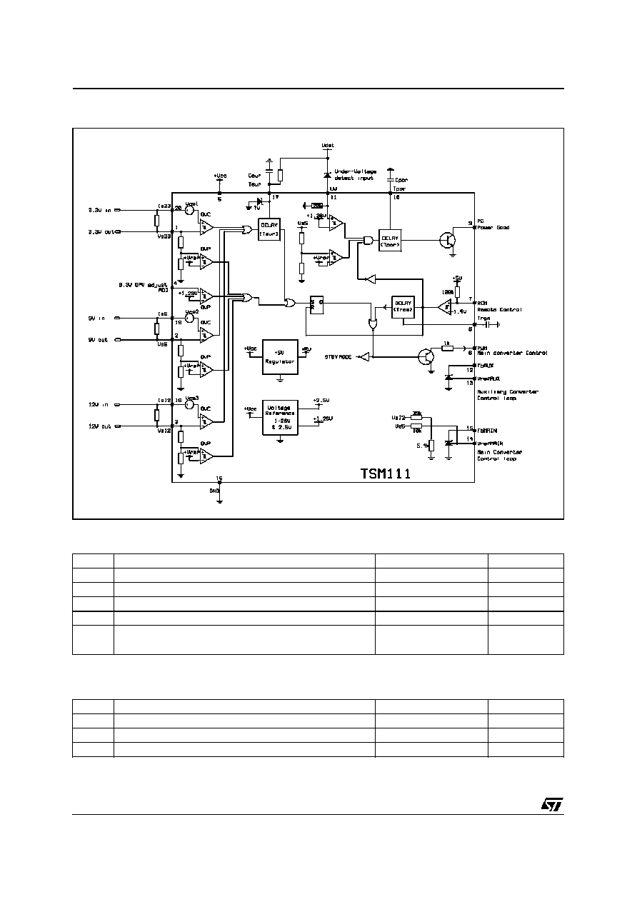
The TSM111 integrated circuit incorporates all
sensing circuit to control a triple output power sup-
ply. It includes voltage references , comparatorsand
matched resistors bridge for overcurrent and over-
voltage detection without the need of any external
components.Timing generatorwith external capaci-
tors, control turn On and Off delays. It provides an
integrated and cost effective solution for simultane-
ous multiple voltage control.
APPLICATIONS
This circuit is designedto be used in SMPS forDesk-
top PC, to supervise currents and voltages of all out-
puts and generate power good information to the
system while managing all timing during transitory
operation.
The IC also manages the standby mode of SMPS
while the PC is in sleep mode.
ORDER CODES
Part
Number
Temperature
Range
Package
N
D
TSM111C
0, +70
o
C
∑
∑
Example : TSM111CD
1
2
3
4
5
6
7
8
9
10
11
12
13
14
15
16
17
18
19
20
Vs33
Vs5
Vs12
ADJ
Vcc
P WM
REM
Tre m
P G
Tpor
Is33
Is5
Is12
Ts ur
GND
FbMAIN
VrefMAIN
VrefAUX
FbAUX
UV
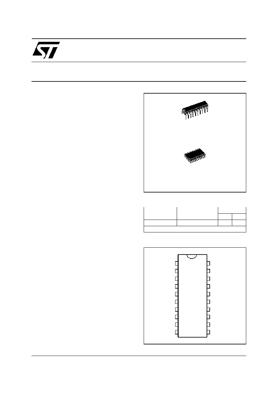
PIN CONNECTIONS (top view)
TSM111
May 1999
N
DIP20
(Plastic Package)
D
SO20
(Plastic Micropackage)
1/18
ABSOLUTE MAXIMUM RATINGS
Symbol
Parameter
Value
Unit
V
CC
DC Supply Voltage pin 5 - note 1
44
V
I
out
Output Current Power Good and PWM
30
mA
P
d
Power Dissipation
1
W
T
stg
Storage Temperature Range
-55 to +150
o
C
ESD
Electrostatic Discharge
2
kV
I
in
Input Current
50
mA
Note : 1.
Al l vol tages val ues, except dif ferenti al voltage, are w ith respect to netw ork ground terminal.
SCHEMATIC DIAGRAM
OPERATING CONDITIONS
Symbol
Parameter
Value
Unit
V
CC
DC Supply Voltage pin 5 - note 2
15 to 36
V
T
oper
Operating Free Air Temperature Range
0 to +70
o
C
I
k
Operating Cathode Current, Vrefaux and Vrefmain
30
mA
Note :
2. The D C supply voltage must be higher than t he maxi mum vol tage applied on the 3.3, 5, 12V inputs
(I s3.3, Is5, Is12) plus 2V.
For example, if 13.2V is present on the I s12 input, the mi nimum required value on V
CC
is 15.2V .
TSM111
2/18

ELECTRICAL CHARACTERISTICS
V
CC
= 16V, T
amb
= 0
o
C to 70
o
C (typical values given for 25
o
C)
Symbol
Parameter
Test Condition
Min.
Typ.
Max.
Unit
I
CC
Total Suppy Current
PG Low
5
10
mA
V
cs1
Current Sense Threshold Voltage 3.3V
46.5
50
53.5
mV
V
cs2
Current Sense Threshold Voltage 5V
46.5
50
53.5
mV
V
cs3
Current Sense Threshold Voltage 12V
60.5
65
69.5
mV
V
iscm
Current Sense Input Common Mode
Voltage Range
see note 2
0
V
CC
-2
V
V
vs1
Overvoltage Sense 3.3V
3.8
4
4.2
V
V
vs2
Overvoltage Sense 5v
5.8
6.1
6.4
V
V
vs3
Overvoltage Sense 12V
13.4
14.2
15
V
V
Adj
Threshold Voltage, 3.3V OVP
Protection.
ADJ input pin4
1.22
1.26
1.3
V
V
sur
Threshold voltage (Tsur input)
2.4
2.5
2.6
V
T
sur
Tsur Timing with Determined External
Components
33k
to V
CC
, 4.7
µ
F to
ground
21
ms
V
surend
Tsur Input Clamp Voltage
7
8
V
V
pull
Input Pulled Down Voltage for V33, V5
and V12
Isink = 100
µ
A,
REMOTE high
0.4
V
VOLTAGE REFERENCE, AUXILIARY CONVERTER (Fbaux)
Symbol
Parameter
Test Condition
Min.
Typ.
Max.
Unit
Vrefaux
Reference Voltage
I
r
= 0.5mA, T
amb
= 25
o
C
2.46
2.5
2.54
V
Iaux
Current Stability
I
r
= 0.5mA to 10mA
20
mV
Taux
Temperature Stability
17
mV
Regliaux
Line Regulation
15 < V
CC
< 36V
1
mV/V
Ioutaux
Output Sinking Current Capability
V
out
> 2V
15
25
mA
VOLTAGE REFERENCE, MAIN CONVERTER (Fbmain)
Symbol
Parameter
Test Condition
Min.
Typ.
Max.
Unit
Vrefmain
Reference Voltage
I
r
= 0.5mA, T
amb
= 25
o
C
2.46
2.5
2.54
V
Imain
Current Stability
I
r
= 0.5mA to 10mA
20
mV
Tmain
Temperature Stability
17
mV
Reglimain
Line Regulation
15 < V
CC
< 36V
1
mV/V
Ioutmain
Output Sinking Current Capability
V
out
> 2V
15
25
mA
Resp
Absolute Precision of the Internal
Resistor Connected to Vrefmain
(39k, 10k, 5.4k)
+-15
%
Resm
Matching of the Internal Resistors
Connected to Vrefmain
(39k, 10k, 5.4k)
+-1
%
TSM111
3/18
POWER GOOD SECTION
Symbol
Parameter
Test Condition
Min.
Typ.
Max.
Unit
Tpor
Turn on Delay for Power Good,
Cpor = 2.2
µ
F
Ic = 20
µ
A typ.,
Vth = 2V typ.
100
300
500
ms
Ic
Tpor Delay Charging Current
12
20
28
µ
A
Vth
Tpor Delay Threshold Voltage
1.8
2
2.2
V
Vhdet
Under Voltage Comparator Hysteresis
20
40
80
mV
Vhpor
Hysteresis on Tpor
200
250
mV
Vdet
Voltage Detect Level
UV Input pin 11
1.22
1.26
1.3
V
Rdet
Load Resistor on Vdetect
UV Input pin 11
20
k
Vvs4
Undervoltage Sense 5V
4.1
4.3
4.5
V
tr
PG Output Rise Time
C
L
= 100pF
1
µ
s
tf
PG Output Fall Time
C
L
= 100pF
300
ns
Vol2
Power Good Output Saturation Level
Ic = 15mA
0.4
V
Ioh2
Power Good Leakage Current Collector
V
out
= 5V
1
µ
A
REMOTE On/Off
Symbol
Parameter
Test Condition
Min.
Typ.
Max.
Unit
Vrem
Remote On/Off Input Threshold Level
1
1.8
V
Iil
Remote Input Low Driving Current
1
mA
Vol1
Remote Output (PWM) Saturation Level
Ic = 0.5mA
1.3
V
Ioh1
Remote Output (PWM) Collector
Leakage Current
Vout = 5V
1
µ
A
Vih1
Remote Input Voltage Level
Pin 7 open
4.2
5.25
V
Trem1
Timing On to Off in to On/Off
out, Cext = 100nF
4
8
14
ms
Trem2
Timing Off to On in to On/Off
out, Cext = 100nF
16
24
34
ms
TSM111
4/18
PIN DESCRIPTION
Name
Pin
Type
Function
V
CC
5
supply
Positive supply voltage. The DC supply voltage must be higher than
the maximum voltage applied on the 3.3, 5, 12V inputs (Is3.3, Is5,
Is12) plus 2V.
For example, if 13.2V is present on the Is12 input, the minimum
required value on V
CC
is 15.2V
Vrefmain
14
analog input
Reference comparison input for main converter regulation loop.
2.5V +-1.6%
Fbmain
15
analog output
Output for main converter regulation loop (optocoupler)
Vrefaux
13
analog input
Reference comparison input for auxiliary converter regulation loop.
2.5V +-1.6%
Fbaux
12
analog output
Output for auxiliary converter regulation loop (optocoupler)
IS33
20
analog input
3.3V overcurrent control sense input.
V33
1
analog input
3.3V overvoltage control sense input.
IS5
19
analog input
5V overcurrent control sense input.
V5
2
analog input
5V overvoltage control sense input.
IS12
18
analog input
12V overcurrent control sense input.
V12
3
analog input
12V overvoltage control sense input.
Adj
4
ana input
Adjustment pin for 3.3V OVP. This pin is to be used for an OVP other
than 3.3V (eg for
µ
C power supply = 2.7V). When not in use, this pin
should be grounded. When in use, V
S33
should not be connected.
Tsur
17
program.
analog input
Overcurrent blank-out time 20 to 30ms settable through external RC.
The voltage at this pin is clamped at typically 5V. Trip voltage = 1.25V.
Rem
7
logic input
Remote On/Off logic input for
µ
C, turn off PWM after Trem delay.
Rem = 0 means that the main SMPS is operational.
Trem
8
program.
analog input
Connected to external capacitor to determine Trem (remote control
delay) timing. Trem (on to off) is 8ms typ. Trem (off to on) is 24ms typ.
Crem = 0.1
µ
F
PWM
6
logic output
Output signal to control the primary side of the main SMPS through
an opto-coupler. When PWM is low, the main SMPS is operational.
Tpor
10
program.
analog input
Connected to external capacitor for Power-on-reset timing.
Cpor = 2.2
µ
F
UV
11
analog input
Undervoltage detection, control and detect main AC voltage failure.
PG
9
logic input
Power Good logic output, 0 or 5V. Power Good high (=1) means that
the power is good for operation.
GND
16
supply
Ground or Negative supply voltage.
TSM111
5/18
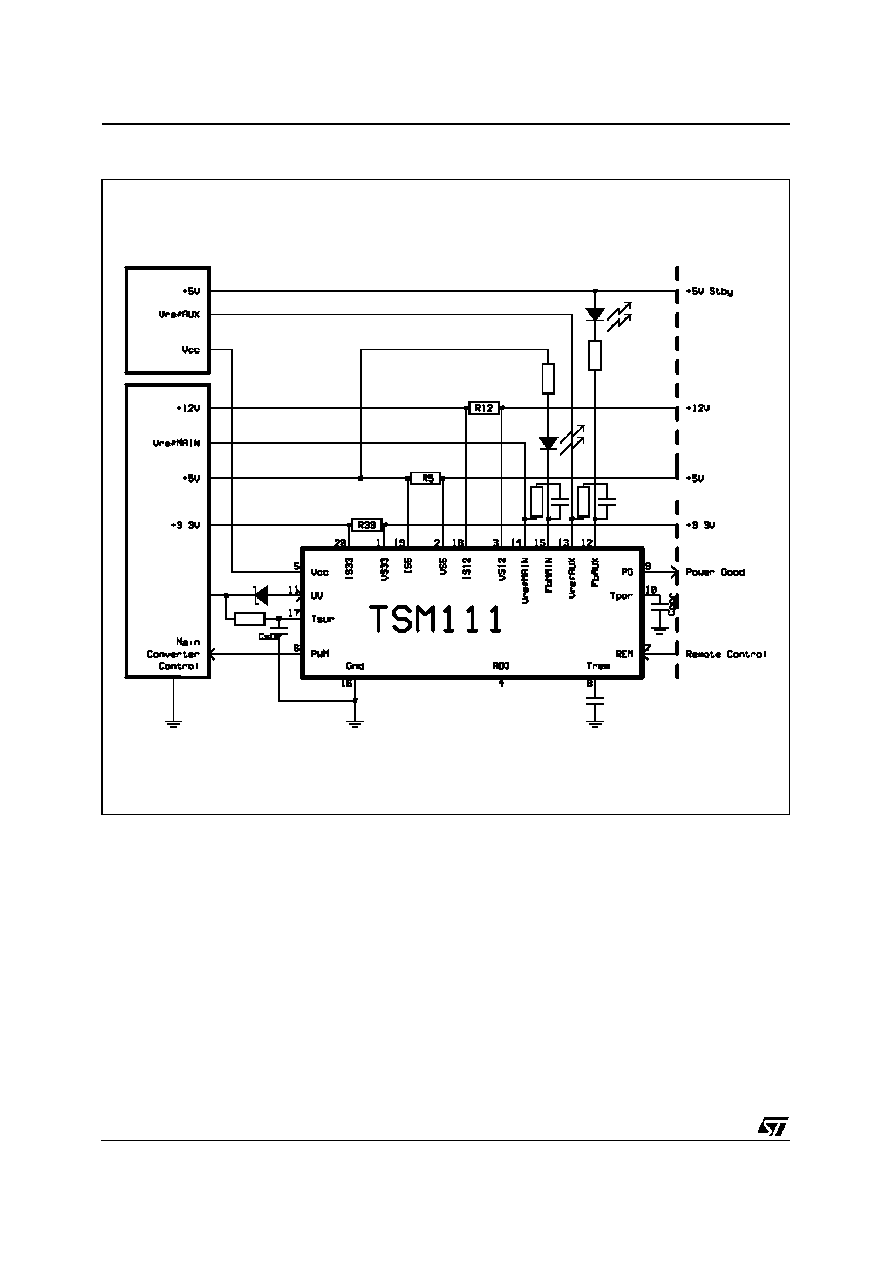
APPLICATION DIAGRAM
TSM111
6/18
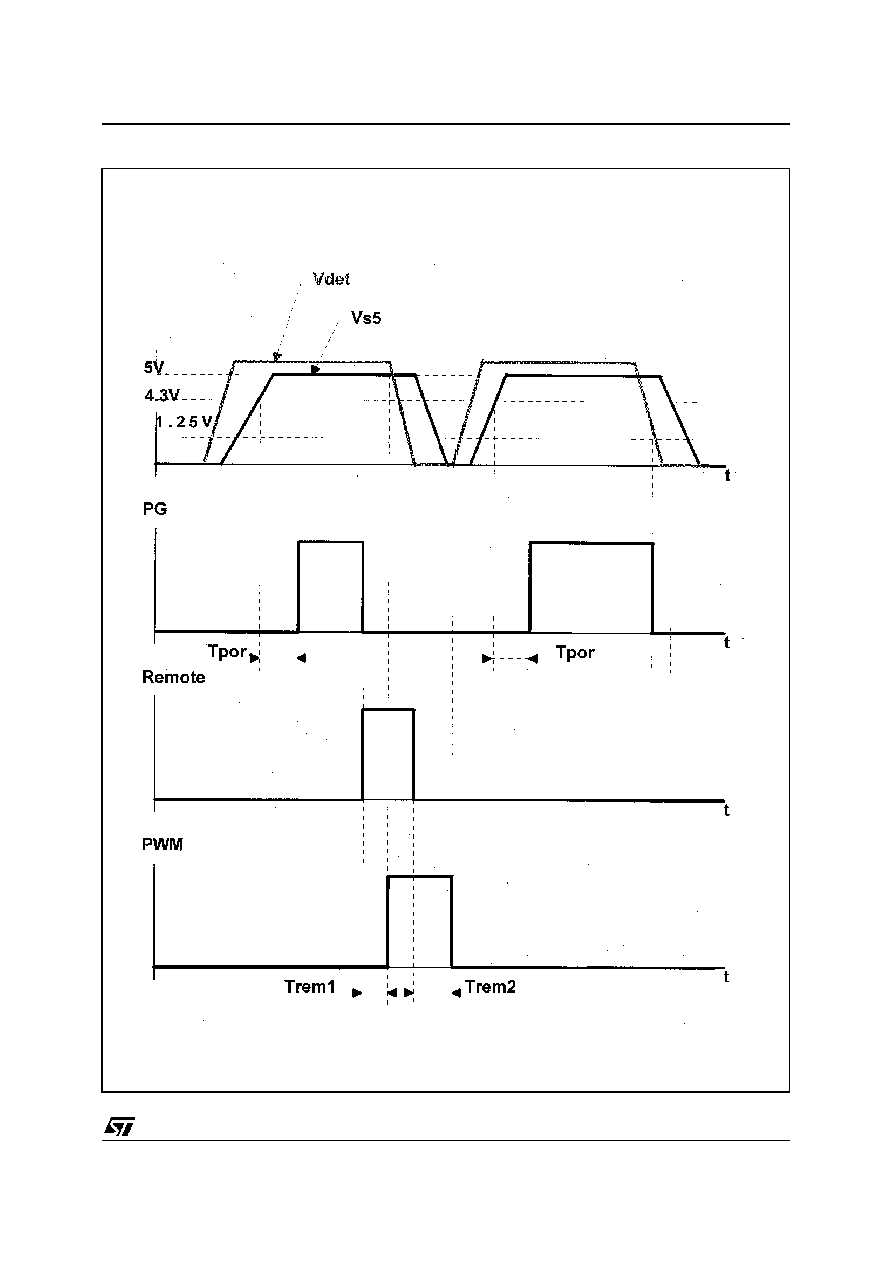
TIMING DIAGRAM : remote control
TSM111
7/18
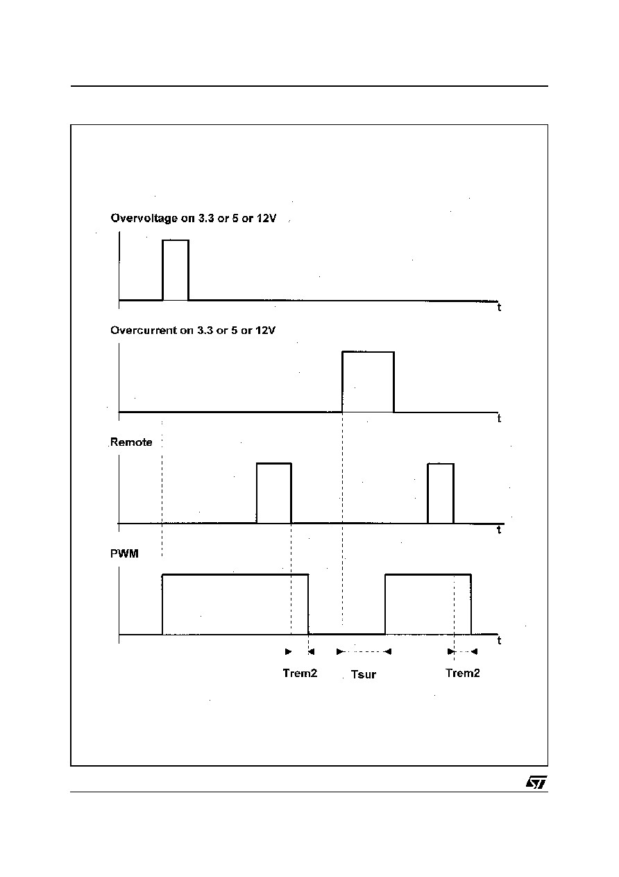
TIMING DIAGRAM : overvoltage or overcurrent shut-down
TSM111
8/18

AN EXAMPLE OF 90W MICRO ATX
POWER SUPPLY USING L5991A, VI-
PER20 AND TSM111
Protection against accidental short circuits and fault
conditions is mandatory in PC power supplies.
These protection circuits can be realized by using
many discrete components which occupy a lot of
PCB space, design time in fine tuning the circuit and
also add to assembling costs.
ST's single chip TSM111 IC provides complete pro-
tection circuits design easier, with fewer number of
components. TSM111 is an ideal supervisor IC for
PC power supplies.
The salient features and benefits of this device are
listed below :
a) Over voltage protectionfor 3.3V,5V and12V with-
out external component.
b) Over current protection for 3.3V, 5V and 12V.
c) Generates Power Good signal.
d) Programmable timing for Power Good signal.
e) Wide range supply operating voltage up to 36V
(44V AMR).
f) Stable internal voltage reference.
g) Two 1.6% voltage reference for Main and Auxil-
iary regulation.
h) Few external components.
i) Circuit occupies little space on PCB.
j) Easy implementation of the circuit.
FEATURE DESCRIPTIONS
a) Over voltage protectioncan be implemented with-
out any additional components. Overvoltage sense
levels for 3.3V, 5V, 12V are 4V, 6.1V, 14.2V respec-
tively. With very little tolerances, better protection is
achieved.
b) Over current protection can be implemented with
very small value sense resistors. As the current
sense threshold levels are set very low, regulation
is not affected. The current sense threshold levels
for 3.3V, 5V, 12V are 50mV, 50mV and 65mV re-
spectively.
c) The power good signal (pin9) is asserted to indi-
cate the 5V and 3.3V is above the under voltage
threshold level. PG pin goes high when the above
condition is reached. Pull up resistor R27 (3.1K) is
connected to 5V STDBY supply from this pin.
d) The timing of the power good signal can be con-
trolled by adjusting the value of the charging capaci-
tor on pin 10. With 2.2
µ
F/16V capacitor on pin 10,
400msec turn on delay is achieved.
e) The power supply can be operated from 14.5V to
36V. The V
CC
must always be higher than the supply
voltage on the 12V input pin by 2V .i.e. if 14V is ap-
pearing 12V input pin the Vcc must be > 16V.
A COMPLETE PC SMPS SECONDARY SUPERVISOR
TSM111
9/18

f) Two internal high precision TL431 shunt regula-
tors are built-in. It provides stable referencevoltages
with a voltage precision of 1.6%.
SUPERVISORY CIRCUIT OPERATION
The system power ON/OFF logic is generated by
the PC, which is "Low" in system "On" condition and
"High" when the system is "Off". This is connected
to remote pin 7.
The IC's internal logic circuit generatesa control sig-
nal on pin 6. In normal operation, when there is no
over voltage or over current at the three inputs, the
voltage on pin 6 follows the Remote pin 7 voltage,
i.e. if the remote pin 7 is low the pin 6 is also low or
vice versa.
When fault is detected on the inputs, control pin 6
goes "High". This control pin 6 output can be used
to turn off the Mains Power Supply during fault con-
dition. An optocoupler is connected directly, with
cathode connected to the IC pin 6 and anode to
5V (from STDBY supply).
In normal operation the voltage on pin 6 is (opto
cathode) is around 3.7 V. On the primary side the
opto transistor collector is pulled through a resistor
to Vref.
It is required to invert the signal before connecting
to the feedback compensation pin 6 of L5991A for
reverse logic. i.e during normal operation the com-
pensation pin is not affected and during fault condi-
tion the pin is pulled Low. Slight delay (R34,C32) is
introduced on the primary side to avoid fault turn on
condition.
Note : Once the fault conditi on is removed, it is required to
reset the Remote pin to make the system functi on again.
TSM111
10/18
No
Part Number
Qt
Manufacturers
Remarks/Descirptions
ICs
1
L5991A
1
ST
Advanced PWM Controller
2
VIPer20DIP
1
ST
Aux controller PWM+Mos
3
TSM111
1
ST
Triple Voltage and Current Supervisor
4
LM7912CV
1
ST
-12V Post Regulator
5
TL431
1
ST
Programmable Voltage Reference
MOSFETs
6
STP6NB80
1
ST
TO220 6A, 800V Mos
7
STP3020L
1
ST
TO220 22mohm 30V Mos
Rectifiers
8
BYV10-40
1
ST
1A, 40V or BYV10-60 or BYW100-200
9
BYW100-200
3
ST
1A, 100V or 200V, BYW100-100
10
STPS20L40CT
1
ST
2x10A, 40V or STPS2045CT or
STPS30L40CT
11
STSPS10L40CT
1
ST
2x5A, 40V
12
KAL04
1
-
3Amp 400VAC Bridge Rectifier or higher
13
1N4148
1
-
Transformers / Inductors
12
HM00-98150
1
BI Tech.**
Aux Transformer
13
HM00-98151
1
BI Tech.
Main Transformer
14
HM00-98148
1
BI Tech.
Coupled inductors
15
HM50-150K
1
BI Tech.
15uH inductors - output filter
16
HM11-51502
1
BI Tech.
2.2uH Inductors - output filter
17
HM28-32022
1
BI Tech.
Common Mode choke - AC input filter
18
10uH
1
-
10uH inductors - output filter
Connectors
19
AC input conn
1
-
20
20-pin conn:
39-01-2200
1
Molex
20pin output connector with terminals
Molex 39-00-0038
21
Fann connector
1
-
22
Fuse 3.5A
1
-
23
NTC
1
Siemens
2.2 ohm
24
TLP621 Optocoupler
3
Toshiba
100% transfer ratio
25
AC switch
1
-
26
115V-230V selector
1
-
BILL OF MATERIAL
The following are the bill of material for the 90W SMPS :
TSM111
11/18
No
Part Number
Qt
No
Part Number
Qt
Capacitors
Resistors
27
47UF/25V
1
52
20K
1
28
3.9NF
1
53
47K,3W
1
29
.47UF/16V
1
54
100K,1/2W
2
30
1NF
2
55
5.1K
1
31
100UF/25
1
56
3 MOHM
1
32
.22UF/250V A.C
2
57
1OR
2
33
1000UF/10V
2
58
10 MOHM
1
34
3300UF/10
1
59
4.7K
5
35
470UF/16V
2
60
68K
1
36
2.2NF
2
61
680R
1
37
2.2UF/16
1
62
39K
1
38
470UF/25V
1
63
3.1K
1
39
4.7NF
4
64
470K
1
40
47UF/16V
1
65
100R
1
41
100UF/25V
3
66
10K
4
42
100UF/25V
1
67
3.3K
1
43
47NF
3
68
5 MOHM
1
44
220UF/200V
2
69
1K
1
45
1000UF/25V
1
70
330R
1
46
2.2UF
1
71
10,1/4W
2
47
1.5NF
1
72
470R
1
48
10NF
1
73
0.68
2
49
.1UF
1
74
6.8K
2
50
3.3NF
1
51
56NF
1
** BI Technolo ies Pte Lte
Phone No: 65 249-1115
F ax No: 65 445-1983
Attn: Kelvi n Lim, Sales Dept
.... continued BILL OF MATERIAL
TSM111
12/18
D1
BRIDGE
F1
3.5A
C31
4.7nF
C1
.22uF/250V A.C
C2
.22uF/250V A.C
LF01
R4
10
R2
6.8K
R5
10
R6
470
C6
.1uF
C5
1.5nF
C8
56nF
C9
4.7nF
C11
1nF
C7
3.3nF
Q1
STP6NB80
R7A
.22
R13
10K
IC4
TLP621
IC5
TLP621
T1
MAINS TRANS
+
C10
47uF/25V
+
C3
220uF/200V
+
C4
220uF/200V
C13
3.9nF
R15
5.1K
+
47uF/25V
D4
1N4148
T2
AUX TRANS
D7
BYW100-200
+
C35
470uF/16
R16
4.7K
I N
3
GND
2
O U T
1
IC7
L7912
IC2
TLP621
D15
BYW100-200
D11
STPS2045CT
C21
2.2nF
C26
2.2nF
+
C40
1000uF/25V
+
C24
3300uF/10
+
C22
1000uF/10V
L2
COUPLEDINDUCTOR
R17
10
D16
BYW100-200
R18
10
D8
BYW100-200
+
C17
100uF/25
R39
5mohm
R17A
3.5mohm
R19
10mohm
D5
OP T
D6
OPT
C12
4.7nF
D2
BYT11-800
R10
47K
C41
2.2uF
C28
2.2uF/16
C51
100nF
R23
680
C
100uF/25V
I C 1
I C 6
A . C
I N P U T
1 0 0 V ~
2 4 0 V
A . C
D13
BYW100-200
D12
BYW100-200
C19
100uF/25V
S2
SW SPST
I C 3
1
2
3
4
5
6
7
8
9
1 0
1 1
12
13
14
15
16
1 7
18
19
20
IS33
U V
A D J
T p o r
P G
T s
u r
R E M
FbAUX
V c c
T r e m
VrefAUX
G n d
VrefMAIN
FbMAIN
P W M
IS12
VS5
IS5
VS12
VS33
S U P E R V I S O R
S1
SWSPST
1
2
4
3
1
2
3
4
3
4
1
2
D12
STP1060CT
D3
OP T
D R A I N
( o u t )
3
2
V c c
1
o s c
c o m p
4
5
6
7
8
V I P E R 2 0
G N D
R11
100K,1/2W
R12
100K,1/2W
C34
100uF/25V
1 2
CN1
CON1
1
2
3
5
7
6
9
8
L3
10uH
C18
470uF/16V
R8
6.8K
R9
4.7K
V F B
S
S
S T B Y
R C T
V R E F
D C - L I M
V c c
O U T I S E N
S G N D
P G N D
C O M P
D C
D I S
V c
5
7
1 6
2
3
4
1 5
1 4
9
8
1 0
1 3
1 2 1 1 6
L 5 9 9 1
IC3
L5991A
1
2 3 4 5 6 7 8 9 1 0
1 11 2
1 3
1 41 5
1 6
1 7
1 8
1 92 0
CON3
CN3
R26
39K
C38
47nF
R27
3.1K
C20
470nF
R7A1
6
4
3
5
2
1
1 2
1 1
1 0
7
8
9
R9
47
C16
1nF
C14
.47uF/16V
R7
1K
D
20V
D5
1N4148
R10
10
Q3
STP3020
D14
OP T
R42
1K
R38
3.3K
C23
1000uF/10V
R47
10K
D14
1N4148
C55
10uF/35V
R
20K
IC10
TL431
R44
330
R
X
R43
4.7K
R45
4.7K
GND ANALOG
R24
10K
Q2
NPN1
R34
10K
L4
2.2uH
+
C25
470uF/16V
R20
4.7K
+
C32
220uF/16V
C30
4.7nF
L6
INDUCTOR
C29
470uF/25V
R22
33K
1
2
F
R29
4.7K
R3
100
R28
470K
VAR
R
OPT
R
OPT
R
680,1/2W
1 2
R
1K
C37
47nF
R
8.2K
5
V S T D
B Y
1
7
V
3
.
3
V
5
V
1 2
V
-
1 2
V
T S M 1 1 1
P
W O
K
P
S O
N
/ O
F
F
NTC
2.2ohm
TSM111
13/18
TSM111 is a Housekeeping IC which is best used
in PC Switch Mode Power Supplies for secondary
3.3V, 5V, and 12V power lines protection.
TSM111 integrates all the necessary functions for a
secure and reliable overcurrent and overvoltage
protection, as well as a logic interface for proper
communication with the motherboard and adjust-
able timing circuitry for optimized sequencing man-
agement. Moreover, TSM111 integrates two pre-
cise shunt voltage references for direct optocoupler
drive. TSM111, integrating the equivalent of more
than 25 discrete components, saves a lot of design
time and fine tuning, as well as PCB area, and in-
creases the reliability of the whole application.
How to use the TSM111 Evaluation Board ?
This evaluation board allows to adapt the TSM111
housekeepingchip to an already existing PC Power
Supply by simply choosing proper values for it's ex-
ternal components, and making the adequate con-
nections to the I/O of the evaluation board.
The Electrical Schematic of the TSM111 evaluation
board is shown on figure 1. It includes the TSM111
as well as the minimum component number re-
quired to make the TSM111 fit in a PC SMPS appli-
cation.
Components calculations
The overvoltage protection is not to be adjusted. In-
ternal voltage thresholds are given by Vvs1, Vvs2,
Vvs3 for respective protection of the 3.3V, 5V, 12V
power lines.
The overcurrent protection is given by the choice of
the Sense resistors R1, R2, R3 (respectively for
eachpower line 3.3V, 5V, 12V). Internalprecise volt-
age thresholds define the tripping voltage drops for
each line following equations 1, 2 & 3 :
Vcs1 = R1 x I33
eq1
Vcs2 = R2 x I5
eq2
Vcs3 = R3 x I12
eq3
where I33, I5, and I12 are the tripping currents.
The system will latch (Fault output will be active -
high) if the overcurrent lasts more than the author-
ized surge delay Tsur given by equations 4 & 5 :
Icharge = Vcc / R4
eq4
Tsur = (C1 x Vsur) / Icharge
eq5
Note that eq4 is an approximation of a capacitive
charge where Vcc (16V min) is large versus the
threshold voltage Vsur (2.5V).
R4=33k
, C1=4.7
µ
F => Tsur=21ms
Thanks to the Tsur adjustment, the normal surge
currents which occur during power up (capacitive
EVALUATION BOARD - TECHNICAL NOTICE
V s 3 3
1
I s 3 3
2 0
I s 5
1 9
V s 5
2
I s 1 2
1 8
V s 1 2
3
V r e f M a i n
1 4
F b m a i n
1 5
V r e f A u x
1 3
F b A u x
1 2
PG
9
Tpor
10
Rem
7
T R e m
8
A d j
4
G n d
1 6
V c c
5
UV
11
Tsur
17
PWM
6
U1
TSM111
R1
rs3.3V
R2
rs5V
R3
rs12V
D1
UV
R4
Rsur
C1
Csur
C2
Crem
R5 R rem
C3
Cpor
R6
1
2
J1
Vdet
1
2
J2
Fault
1
2
J3
Optaux
1
J5
In3.3V
1
J6
1
J7
In3.3V
Vdet
Optaux
Fault
In5V
In12V
Out12V
Out5V
Out3.3V
1
J8
Out12V
1
J9
Out5V
1
J10
Out3.3V
PG
1
2
J11
PG
1
2
3
4
SW1
BP Rem
1
2
J12
Rem
Fro m c
5Vstby
5Vstby
1
2
J13
Vcc
1
2
J14
Gnd
VCC
1
2
J15
VrefMain
VrefMain
R7
RoptMain
VrefAux
R8
R9
Roptaux
C4
C5
1
2
J16
VrefAux
R10
1
2
J20
D5
D6
I
1INV
1
2
J18
OptMain
OptMain
Vin
2
G N D
1
Vout
3
U2 78L05
5Vstby
+
C7
R11
5Vstby
In5V
IN12V
EVALUATION BOARD - ELECTRICAL SCHEMATIC
C6
TSM111
14/18
loads charging) are blanked for a time dependingon
each application.
When the system has latched (either after overcur-
rent or overvoltage condition), the system needs to
be reset via the Remote input. The C2 capacitor de-
termines two different timings to the Fault output :
C2=100nF => Trem1(ON to OFF)=8ms
C2=100nF => Trem2(OFF to ON)=24ms
R5 is a pull down resistor on the remote pin of
TSM111. Note that an integrated pull up resistor of
100k
is to be taken into account in the choice of
R5, knowing that the threshold voltage of the input
comparator is 1.4V. Therefore, R5 should be lower
than 38.8k
.
R5 = 1k
is a good value.
The evaluation board integrates the possibility to
make theRemote signaleither manual, or electronic
thanks to the ORing diodes D5 and D6 (and the pull
down resistor R5), and the Push Button (SW1).
These diodes can of course be replaced by straps
according to the evaluation requirements (manual
or electronic).
The Tpor delay time allows the PG output (Power
Good) to rise to high level when the 5V power line
internal supervision circuitry has stayed above the
undervoltage 4.3V threshold for more than Tpor
time following the approximated equation 6 :
C3 x Vth = Ic x Tpor
eq6
where Vth is 2V and Ic is 20
µ
A.
C3=2.2
µ
F => Tpor=300ms
When the 5V power line passes under the 4.3V un-
dervoltage threshold, the Power Good signal (PG)
falls immediately to low level.
The Power Good output can also be triggered by the
Vdet input of the board. This input should be con-
nected to a power line representative of the AC
mains power situation. As an example, an additional
winding on the auxiliary power supply offer an early
warning of power down from the mains power point
of view. The UV threshold is internally fixed to
Vdet=1.26V. Therefore, it is necessary to add a
zener diode D1.
D1=15Vzener => Vdet=16.26V
Note that a 20k
serial pull down resistor is inte-
grated. Therefore, only a low power zener is
needed.
The Fault output needs a pull up resistor R6.
The Power Good output needs a pull up resistor
R11. Both signals are pulled up to the 5Vstandby
power supply which can be generated from the
evaluation board thanks to a 78L05 5V regulator.
This regulator needs a C6 bypass capacitor. The C7
bypass capacitor smoothens the V
CC
pin of
TSM111.
The Adj (Adjust) pin shouldbe connectedto ground.
Adjust allows to tune a new overvoltage protection
value (ex 2.7V instead of 3.3V).
Example of component lists
Table 1 gives an example of component list
Name
Type
Value
Comment
U1
IC
TSM111
DIP20
U2
IC
78L05
TO92
R1
R 1/4W
R 1/2W
R 1W
10m
5m
2.5m
5A
10A
20A
R2
R 1/4W
R 1/2W
R 1W
10m
5m
2.5m
5A
10A
20A
R3
R 1/4W
R 1/2W
R 1W
65m
13m
6.5m
1A
5A
10A
R4
R 1/4W
33k
R5
R 1/4W
1k
R6
R 1/4W
47k
R7
R 1/4W
depends on opto used
R8
R 1/4W
10k
comp. network to
be fine tuned
R9
R 1/4W
depends on opto used
R10
R 1/4W
10k
comp. network to
be fine tuned
R11
R 1/4W
47k
D1
Z 1/4W
15V
D5
D 1/4W
1N4148
D6
D 1/4W
1N4148
C1
C Electro
4.7
µ
F
C2
C Plastic
100nF
C3
C Electro
2.2
µ
F
C4
C Plastic
10NF comp. network to
be fine tuned
C5
C Plastic
10NF comp. network to
be fine tuned
C6
C Plastic
100nF
C7
C Electro
10
µ
F
Figures 2a and 2b show the copper and silkscreen
sides of the Evaluation board PCB.
Note that it is not a 1/1 scale.
TSM111
15/18
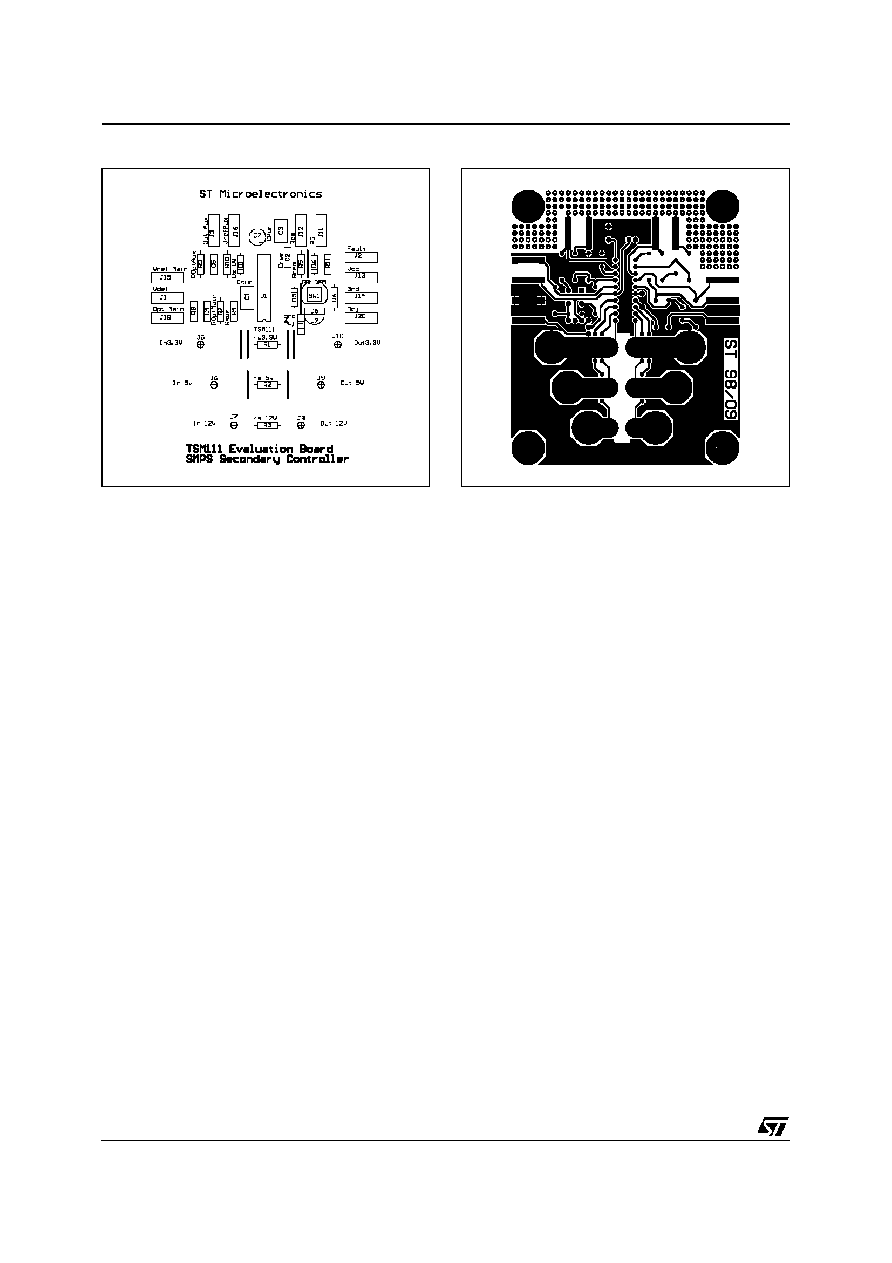
Figure 2a
Figure 2b
TSM111
16/18
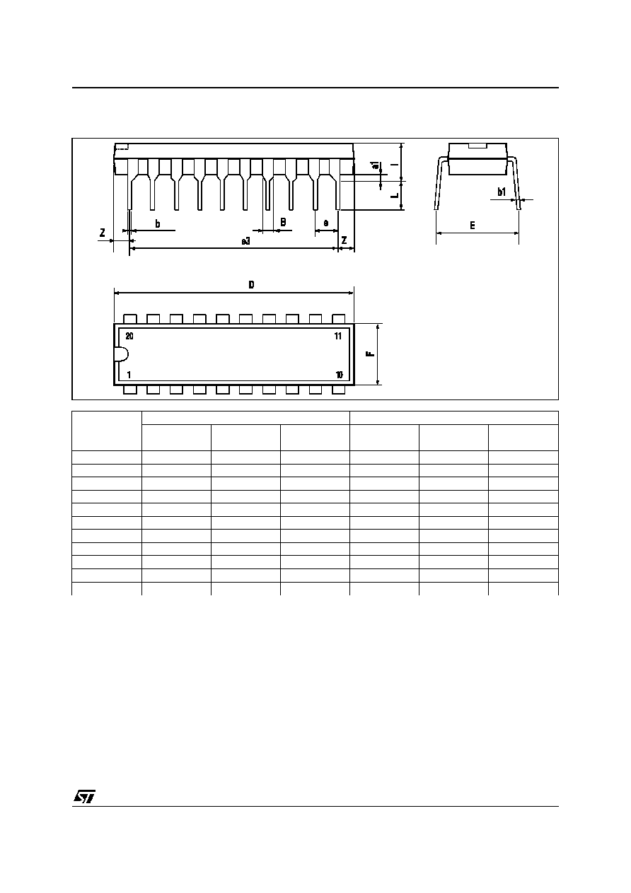
PACKAGE MECHANICAL DATA
20 PINS -PLASTIC DIP
Dimensions
Millimeters
Inches
Min.
Typ.
Max.
Min.
Typ.
Max.
a1
0.254
0.010
B
1.39
1.65
0.055
0.065
b
0.45
0.018
b1
0.25
0.010
D
25.4
1.000
E
8.5
0.335
e
2.54
0.100
e3
22.86
0.900
F
7.1
0.280
I
3.93
0.155
L
3.3
0.130
Z
1.34
0.053
TSM111
17/18
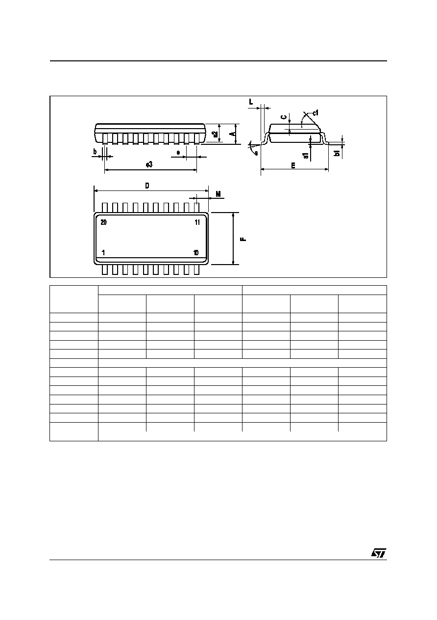
PACKAGE MECHANICAL DATA
20 PINS -PLASTIC MICROPACKAGE (SO)
Dimensions
Millimeters
Inches
Min.
Typ.
Max.
Min.
Typ.
Max.
A
2.65
0.104
a1
0.1
0.3
0.004
0.012
a2
2.45
0.096
b
0.35
0.49
0.014
0.019
b1
0.23
0.32
0.009
0.013
C
0.5
0.020
c1
45
o
(typ.)
D
12.6
13.0
0.496
0.512
E
10
10.65
0.394
0.419
e
1.27
0.050
e3
11.43
0.450
F
7.4
7.6
0.291
0.299
L
0.5
1.27
0.020
0.050
M
0.75
0.030
S
8
o
(Max.)
Information furnished is believed to be accurate and reliable. However, STMicroelectronics assumes no responsibility for the
consequences of use of such information nor for any infringement of patents or other rights of third parties which may result
from its use. No license is granted by implication or otherwise under any patent or patent rights of STMicroelectronics.
Specifications mentioned in this publication are subject to change without noti ce. This publication supersedes and replaces all
information previously supplied. STMicroelectronics products are not author ized for use as critical components in life support
devices or systems without express written approval of STMicroelectronics.
©
The ST log o is a trademark of STMicroelectronics
©
1999 STMicroelectronics ≠ Printed in Italy ≠ All Rights Reserved
STMicroelectronics GROUP OF COMPANIES
Australia - Brazil - Canada - China - France - Germany - Italy - Japan - Korea - Malaysia - Malta - Mexico - Morocco
The Netherlands - Singapore - Spain - Sweden - Switzerland - Taiwan - Thailand - United Kingdom - U.S.A.
©
http://www.st.com
TSM111
18/18