Revision A
1/11
s
Over voltage protection for 3.3V 5V and
12V without external components
s
Under voltage protection for 3.3V 5V and
12V without external components
s
Over voltage protection for -12V or -5V with
external components
s
Externally adjustable under voltage
blanking during power up
s
Power good input/output
s
Externally adjustable pg delay
s
Fault output
s
Remote output
s
Externally adjustable remote delay
s
Precision voltage reference
s
2kV ESD protection
DESCRIPTION
The TSM1121 integrated circuit incorporates all
sensing circuitry to regulate and protect from over
voltage and under voltage a multiple output power
supply (3.3V, 5V and 12V).
TSM1121 incorporates all the necessary functions
for Housekeeping features which allow safe
operation in all conditions, and very high system
integration.
TSM1121 integrates a precise voltage reference.
APPLICATION
s
PC SMPS triple power line housekeeping ic
(3.3V 5V 12V)
ORDER CODE
Note: N = Dual in Line Package (DIP)
D = Small Outline Package (SO) - also available in Tape &
Reel (DT)
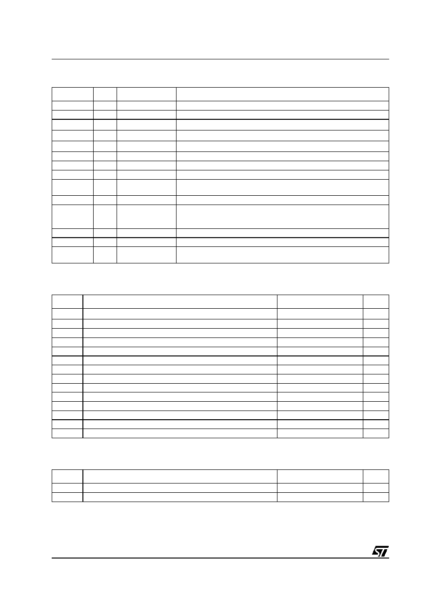
PIN CONNECTIONS (top view)
Part
Number
Temperatur
e Range
Package
Marking
N
D
TSM1121CN
0 to 85�C
�
TSM1121C
TSM1121CD
0 to 85�C
�
M1121
N
DIP14
(Plastic Package)
D
SO14
(Plastic Micropackage)
VCC
REM
TREM
TPG
PG
VS33
VS5
VS12
PI
TUV
EP
GND
VREF
10
9
8
7
6
5
4
3
2
1
11
12
13
14
FAULT
TSM1121
3.3V 5V 12V HOUSEKEEPING IC
May 2003
TSM1121
Pin Description
2/11
1 PIN DESCRIPTION
ABSOLUTE MAXIMUM RATINGS
OPERATING CONDITIONS
Name
Pin #
Type
Function
Vcc
14
Power Supply
Positive Power Supply Line
Gnd
7
Power Supply
Ground Line. 0V Reference For All Voltages
Vs12
3
Analog Input
Over and Under voltage Sense Input Dedicated to the 12V Line
1
1)
Over and Under Voltage Inputs can go higher than Vcc within the allowed Max Rating range
Vs5
2
Analog Input
Over and Under voltage Sense Input Dedicated to the 5V Line
1)
Vs33
1
Analog Input
Over and Under voltage Sense Input Dedicated to the 3.3V Line
1)
Tuv
6
Timing Capacitor
Adjustable Under voltage Blanking Delay at Power Up (Setting Capacitor)
Fault
13
Open Collector
Fault Output. Fault is high when Over or Under Voltage has been Detected
PI
5
Analog Input
Power Good Input. Detection of the Power Conditions
PG
12
Open Collector
Power Good Output. PG output is High when the Power Conditions are
OK
Tpg
11
Timing Capacitor
Adjustable Power Good Delay (Setting Capacitor)
REM
9
Logic Input
Input Remote Control of the Complete System by the Motherboard (
�
Con-
troller). Remote is active high. Switch OFF/ON of the Power Supply. Reset
of the Complete System after a FAULT Activation.
Trem
10
Timing Capacitor
Adjustable Remote Delay (Setting Capacitor).
Vref
8
Voltage Reference
2.5V Reference for all Voltages
EP
4
Analog Input
Extra Protection Circuit. Can be used for -12V or -5V Over Voltage Protec-
tion.
Symbol
DC Supply Voltage
Value
Unit
Vcc
DC Supply Voltage
1
25
V
Iout
Output Current Power Good
30
mA
Io
Output current for the Voltage reference
20
mA
VFault
Fault Ouput
5
V
Pd
Power Dissipation
0.7
W
Tstg
Storage Temperature
-55 to 150
�C
ESD
Electrostatic Discharge
2
kV
Tuv
Adjustable Under voltage Blanking At Power UP
5
V
EP
Extra Protection
5
V
PI
Power Good Input
5
V
PG
Power Good Output
5
V
Tpg
Adjustable Power Good Delay
5
V
REM
Remote Control
5
V
Trem
Adjustable Remote Delay
5
V
1)
All voltage values, except differential voltage are with respect to network ground terminal.
Symbol
Parameter
Value
Unit
Vcc
DC Supply Conditions
4.5 to 24
V
Toper
Operating Free Air Temperature Range
0 to 85
�C
Electrical Characteristics
TSM1121
3/11
2 ELECTRICAL
CHARACTERISTICS
Tamb = 25�C and Vcc = 17V (unless otherwise specified)
Symbol
Parameter
Test Condition
Min
Typ
Max
Unit
Total Current Consumption
Icc
Total Supply Current
3
5
mA
Over Voltage and Under Voltage Protection
Vov33
Over Voltage Sense 3.3V
Input can go higher than
Vcc
3.8
4
4.2
V
Vov5
Over Voltage Sense 5V
Input can go higher than
Vcc
5.8
6.1
6.4
V
Vov12
Over Voltage Sense12V
Input can go higher than
Vcc
13.4
14.2
15
V
Vuv33
Under Voltage Sense 3.3V
2.1
2.3
2.5
V
Vuv5
Under Voltage Sense 5V
3.7
4
4.3
V
Vuv12
Under Voltage Sense 12V
9.2
10
10.8
V
Vep
Extra Over voltage Protection Threshold
1.28
V
Tfault
Fault Delay Before Latching
Internally Fixed Delay
100
�
s
Under Voltage Blanking During Power Up
Tuv
Under Voltage Blanking During Power
Up (Vcc rising)
Cuv = 2.2
�
F
Adjustable Blanking
100
300
500
ms
Thuv
Blanking Threshold
1.28
V
Power Good (PG)
Vpgth
Power Good Voltage Threshold
1.28
V
Vpghyst
Power Good Voltage Threshold Hyster-
esis
70
mV
Vpgol
Low Output Open Collector Saturation
Voltage
Collector Current = 15mA
0.4
V
Ipgoh
High Output Open Collector Leakage
Current
PG Output = 5V
1
�
A
Tpgr
Power Good Output Rise Time
Load Capacitor = 100pF
1
�
s
Tpgf
Power Good Output Fall Time
Load Capacitor = 100pF
1
�
s
Tpg
Power Good Adjustable Delay
Load Capacitor Cpg=2.2
�
F
100
300
500
ms
PIth
Power Input Detection Threshold
1.28
V
Fault
Vfaultol
Fault Output Saturation Voltage Level
IFault = 1mA
1
V
Ifaultoh
Fault Output Leakage Current Level
Vfault = 5V
1
�A
Remote Control (REM)
Vremth
Remote ON/OFF Input Voltage Thresh-
old
0.7
0.8
1
V
Vremih
High Input Remote Voltage
3.3
3.4
V
Iremil
Low Input Remote Saturation Current
0.5
mA
Trem1
Remote Adjustable Delay ON to OFF
Load Capacitor
Crem=0.1
�
F
40
50
60
ms
Trem2
Remote Adjustable Delay OFF to ON
Load Capacitor
Crem=0.1
�
F
40
50
60
ms
Voltage Reference
Vref
Internal Voltage Reference
Io = 0mA
2.46
2.5
2.54
V
Regline
Line regulation
Io = 0mA
4.5V<Vcc<24V
4
10
mV
Regline
Line regulation
Io = 10mA
4.5V<Vcc<24V
15
mV
Regload Load regulation
1
1)
Do not short circuit the Vref Pin
0<Io<10mA
25
mV
TSM1121
Electrical Characteristics
4/11
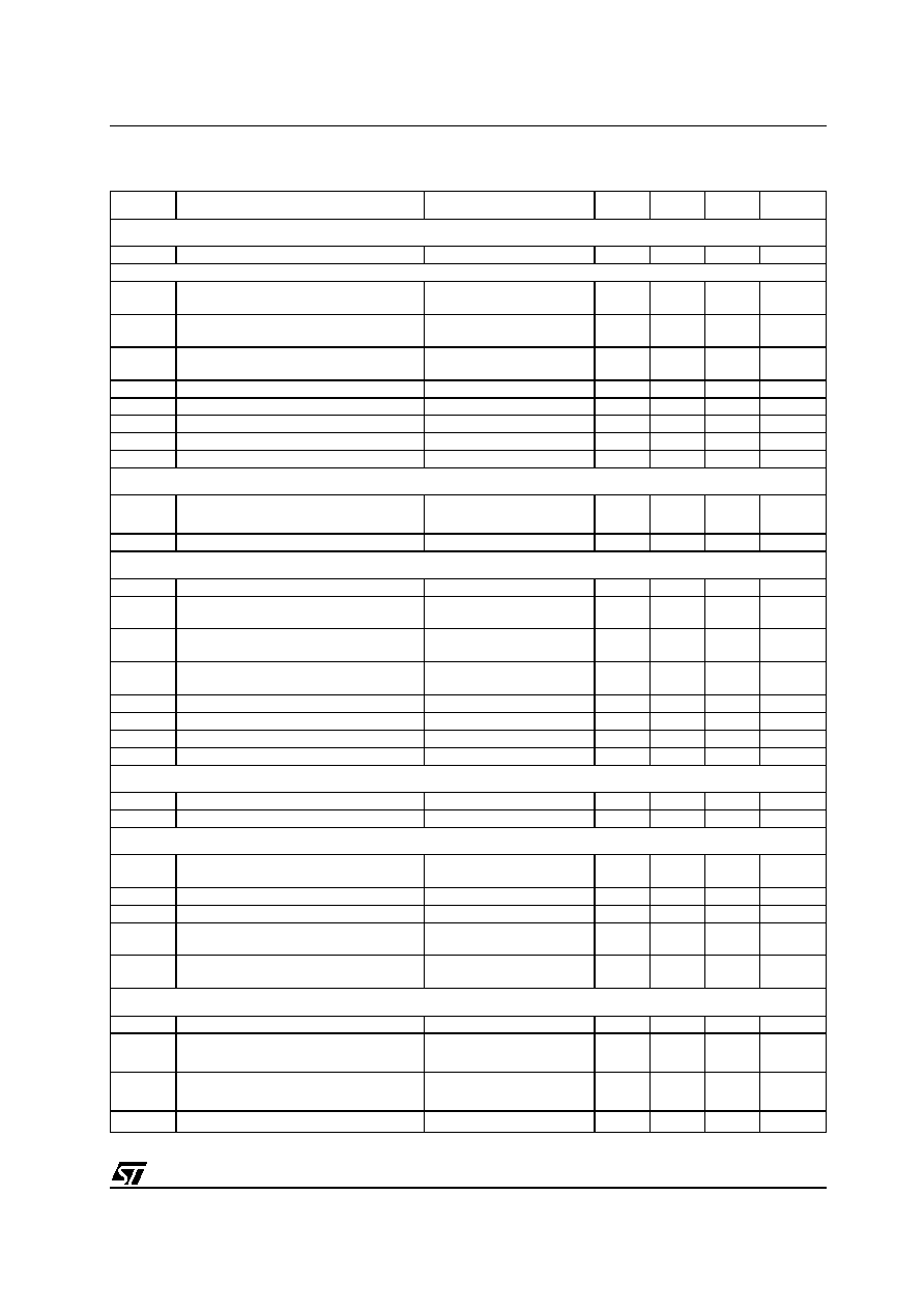
Fig. 1: Application Schematic
Fig. 2: Internal Schematic
PRIMARY
RECT.
MAIN
CONV.
12V
5V
3.3V
AUX.
CONV.
5Vstby
Vcc
~
TSM1121
Over & Undervoltage Protection
Reference
Logic
Sequencer
12V
5V
3.3V
5Vstby
PG
REM
FAULT
PWM + OPTO
PWM + OPTO
+ Vref
+ Vref
OVP
Vref
HOUSEKEEPING
LOGIC
SECONDARY
Vcc
Vs12
Vs5
Vs33
PG
REM
to
M
O
T
H
ER
BO
AR
D
FROM
MAIN
CONV.
POWER
SUPPLY
OUTPUT
12V
5V
3.3V
12V
5V
3.3V
PI
TO
UVP
Trem
Tpg
UV
BLANK
Tuv
FAULT
Gnd
TSM1121
Vref
Ep

Electrical Characteristics
TSM1121
5/11
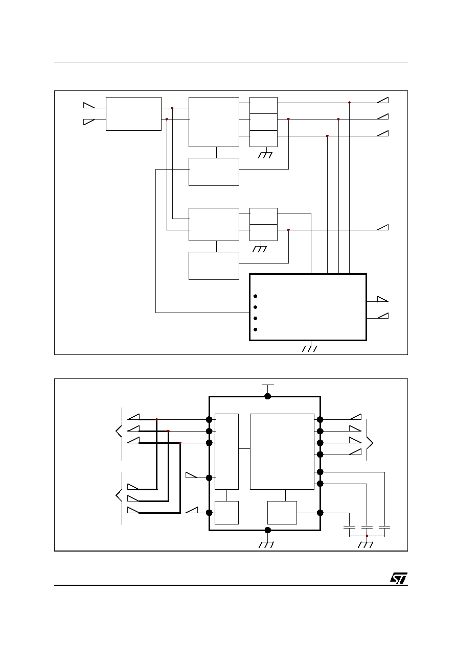
Fig. 3: Detailed Internal Schematic
Vov12
VS12
VS5
VS33
0.8V
FAULT
Rem
Pg
3.47V
S
R
Q
Vcc
PI
VREF
Vuv12
Tfault
Tpg
Cpg
Trem
Cuv
Tuv
Vov5
Vuv5
Vov33
Vuv33
OVP
UVP
TSM1121
Crem
Trem
3.47V
Gnd
Vref
1.25V
VovEP
EP
1k
Vref
Vref
Vref
3
2
1
4
7
8
5
11
9
12
6
10
13
14
1.28V
3.47V
1.28V
1.28V