 | –≠–ª–µ–∫—Ç—Ä–æ–Ω–Ω—ã–π –∫–æ–º–ø–æ–Ω–µ–Ω—Ç: TSM115 | –°–∫–∞—á–∞—Ç—å:  PDF PDF  ZIP ZIP |
July 2004
1/17
s
Over voltage and under voltage protection
for 3.3V +5V and ±12V without external
components
s
Over current protection for 3.3V 5V and
12V with external components
s
Under voltage blanking fonction
s
Power good input/output
s
Externally adjustable PG delay
s
Fault output
s
Remote output
s
Externally adjustable remote delay
s
2kV ESD protection
DESCRIPTION
The TSM115 integrated circuit incorporates all
sensing circuitry to protect from over and under
voltage and over current a multiple output power
supply (3.3V, +5V and ±12V).
TSM115 incorporates all the necessary functions
for Housekeeping features which allow safe
operation in all conditions, and very high system
integration.
APPLICATION
s
PC SMPS Multiple Power Line
Housekeeping IC (3.3V +5V ±12V)
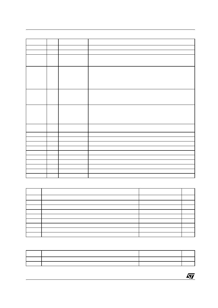
PIN CONNECTIONS (top view)
ORDER CODE
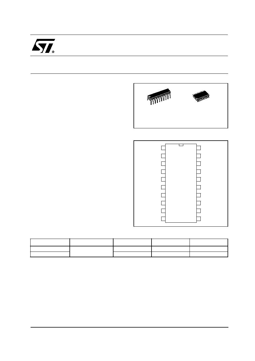
N
DIP-20
(Plastic Package)
D
SO-20
(Plastic Micropackage)
Fault
Gnd
PG
Tuv/Tpg
Rem
Trem/Tsur Vs-12
Bsense
1
2
3
4
5
6
7
8
Vcc
Is3.3
Rcrnt
Vs3.3
Is12
Vs12b
Is5
Vs5
9
10
11
12
13
14
15
16
17
18
19
20
Vs12a
nc
nc
nc
Part Number
Temperature Range
Package
Packaging
Marking
TSM115CN
0 to 95∞C
DIP
Tube
TSM115C
TSM115CD
SO
Tube or Tape & Reel
M115
This is preliminary information on a new product now in development or undergoing evaluation. Details are subject to change without notice.
TSM115
PRELIMINARY DATA
3.3V
+
5V
±
12V Housekeeping IC
TSM115
Pin Description
2/17
1 Pin
Description
ABSOLUTE MAXIMUM RATINGS
OPERATING CONDITIONS
Name
Pin #
Type
Function
Fault
1
Open collector
Fault output. Output of the over voltage and under voltage comparators.
Gnd
2
Power supply
Signal ground and silicon substrate
PG
4
Open collector
Output of the Tpg comparator. This pin goes low upon an under voltage
condition. Except for the delay set by the Tpg capacitor this pin always
reflects the actual state of the under voltage sensing comparators output.
Tuv/Tpg
5
Timing capacitor
A capacitor from this pin to Gnd provides a delay between outputs rail volt-
age within regulation and PG output going high. Capacitor discharges
whenever Bsense low or Rem high or UVP is detected.
This capacitor will also provide the under voltage blanking function when
the voltage at this pin is larger than the Vref voltage. The under voltage
function resume.
Rem
6
Control Input pin
Pulling this pin high will send the Fault pin high latching off the power sup-
ply, reset the internal latch, discharge the start-up timing capacitors, Tuv
and Tpg capacitors, allowing normal start up of the system. Pulling this pin
low will send the Fault pin low, initiating a normal start up function.
Trem/Tsur
7
Timing capacitor
A capacitor from this pin to Gnd will delay the Fault signal when the Rem
pin is used to shut down the power supply. The PG will signal a power fail-
ure warming immediately, but the Fault pin shut down of the power will be
delayed. This capacitor will also provide the overcurrent blanking function
(surge current).
Bsense
9
Control input pin
Non inverting input to the Bsense voltage sensing comparator. Pulling this
pin lower than 2.5V will cause PG goes low and Tuv goes low.
Vs5
10
Analog input
Over voltage and under voltage detection for +5V rail
Is5
11
Analog Input
5V overcurrent control sense input.
Vs12a
12
Analog input
Over voltage and under voltage detection for +12V rail
Vs12b
13
Analog input
Over voltage and under voltage detection for +12V rail
Vs-12
14
Analog input
Over voltage and under voltage detection for -12V rail.
Is12
15
Analog Input
12V overcurrent control sense input.
Vs3.3
16
Analog input
Over voltage and under voltage detection for 3.3V rail.
Is3.3
17
Analog Input
3.3V overcurrent control sense input.
Rcrnt
19
Analog input
A resistor from this pin to Gnd will provide the internal constant current.
Vcc
20
Power supply
Supply input voltage
Symbol
DC Supply Voltage
Value
Unit
Vcc
DC Supply Voltage
1
-0.3 to 18
V
Vpmax
Terminal voltage Vs3.3, Is3.3, Vs12, Is12, Vs5, Is5
-0.3 to 18
V
Vnmax
Terminal voltage Vs-12
-15 to 5
V
VDBTT
VTpg/Tuv, VTrem/Tsur input voltage
-0.3 to 3.3V
V
VTER
Other terminals
-0.3 to Vcc
V
PT
Power dissipation
1
W
Tstg
Storage temperature
-55 to 150
∞C
Tj
Junction temperature
150
∞C
ESD
Electrostatic Discharge
2
kV
1) All voltage values, except differential voltage are with respect to network ground terminal.
Symbol
Parameter
Value
Unit
Vcc
DC Supply Conditions
3 to 15
V
Toper
Temperature range
0 to 95
∞C
Electrical Characteristics
TSM115
3/17
2 Electrical
Characteristics
Tamb = 25∞C, Vcc=5V, Vs3.3=3.3V, Vs5=5V, Vs12= 12V, Vs-12=-12V, Rem=Low, Rcrnt=12k
Symbol
Parameter
Test Condition
Min
Typ
Max
Unit
Total Current Consumption
Icc
Total Supply Current
1
mA
Iccstdby
Total Supply Current in Stand-by Condi-
tions
Rem=high
Vs3.3=0V, Vs5=0V
Vs12=0V, Vs-12=0V
1
mA
Vccmin
Min operating Vcc
Tmin < Tamb < Tmax
3
V
Over Voltage and Under Voltage Protection
Vov12
Over Voltage Sense 12V
13.6
14
14.4
V
Vuv12
Under Voltage Sense 12V
8.85
9.12
9.39
V
Iin12b
Input current Voltage sense 12V
50
100
200
µA
Vov5
Over Voltage Sense 5V
6.01
6.20
6.39
V
Vuv5
Under Voltage Sense 5V
4.00
4.12
4.24
V
Iin5
Input current Voltage Sense 5V
50
100
200
µA
Dis5
Disable Voltage Sense 5V
7
7.5
8
V
Vov3.3
Over Voltage Sense 3.3V
3.88
4.00
4.12
V
Vuv3.3
Under Voltage Sense 3.3V
2.52
2.60
2.68
V
Iin3.3
Input current Voltage Sense 3.3V
25
50
100
µA
Vov-12
Over Voltage Sense -12V
-15.49
-15.04
-14.59
V
Vuv-12
Under Voltage Sense -12V
-9.99
-9.70
-9.41
V
Iin-12
Input current Voltage sense -12V
-200
-100
-50
µA
Dis-12
Disable Voltage Sense -12V
3.3
V
Internal delay time
Tdelay
Internal time
30
37
45
µs
Over current Protection
Is3.3
Current source
46
50
54
µA
Vicm3.3
Input common mode
0.7
Vov3.3
V
Vio3.3
Input offset voltage
2
3
mV
Is5
Current source
46
50
54
µA
Vicm5
Input common mode
0.7
Vov5
V
Vio5
Input offset voltage
2
3
mV
Is12
Current source
46
50
54
µA
Vicm12a
Input common mode
0.7
Vov12
V
Vio12a
Input offset voltage
2
3
mV
Vicm12b
Input common mode
0.7
Vov12
V
Vio12b
Input offset voltage
2
3
mV
Iin12a
Input current
10
µA
Bsense
Thbs
Bsense voltage threshold
1.218
1.282
V
Ilbs
Bsense current leakage
Bsense=1V
0
1
µA
Iobs
Current source
Bsense=1.5V
90
100
110
µA
DIobsT
Current source drift in temperature
Tmin < Tamb < Tmax
5
µA
Vbsoh
Clamp voltage
IoBsense=1µA
2.00
2.15
2.30
V
Iclbs
Clamping current
Bsense > 2.5V
Tmin < Tamb < Tmax
3
3.6
5
mA
Vinbs
Input voltage
-0.3
2.5
V
TSM115
Electrical Characteristics
4/17
Rem
THrm
High threshold
From Low to high
1.87
1.93
1.99
V
TLrm
Low threshold
From high to low
1.0
1.25
1.4
V
Power Good (PG)
Ipgol
Sink current
VPg=0.4V
10
mA
Vpgol
Low output voltage
Ipg=10mA
0.4
V
Tpgr
Rise time PG
Rpg=1K
500
ns
Under Voltage Blanking (Tuv) and Power Good (Tpg) times
Iotuvtpg
Current output source
Vtuvtpg = 0V
4.5
5
5.5
µA
THtuv
High threshold blanking
From low to high voltage
0.287
0.312
0.337
V
TLtuv
Low threshold blanking
From high to low voltage
0.25
V
THtpg
High threshold power good
From low to high voltage
1.218
1.25
1.282
V
TLtpg
Low threshold power good
From high to low voltage
0.9
1
1.1
V
Idtuvtpg
Current discharge of TuvTpg
2
5
mA
Vtuvtpgol
Low output voltage
Iotutpg = 1mA
0.2
V
Vtuvtpgoh Clamp voltage
2.1
2.3
2.5
V
VinTuvTpg Input voltage
-0.3
2.3
V
DIotuvtpg
Current source drift in temperature
Tmin < Tamb < Tmax
1
µA
Remote (Trem) and Surge current blanking (Tsur) times
Iotrm
TRem current source
Vtrmtsur = 0V
90
100
110
µA
Iotsur
Tsur current source
Vtrmtsur = 0V
9
10
11
µA
THtrm
High thresold voltage TRem
From low to high
1.218
1.25
1.282
V
TLtrm
Low thresold voltage TRem
From high to low
0.9
1
1.1
V
Idtrmtsur
Current discharge of TRemTsur
2
5
mA
Vtrmtsurol Low output voltage
Iotmtsur = 1mA
0.2
V
Vtrmtsuroh Clamp voltage
2.1
2.3
2.5
V
Vintrmtsur Input voltage
-0.3
2.3
V
DIotrm
Current source drift in temperature
Tmin < Tamb < Tmax
5
µA
DIotsur
Current source drift in temperature
Tmin < Tamb < Tmax
500
nA
Fault
Ifltol
IFault sink current
VFault=0.4V
10
mA
Vfltol
Low output voltage
IFault=10mA
0.4
V
THVcc
High threshold voltage, Vcc low to high
Rem low, all lines between
UV and OV.
2.95
V
TLVcc
Low threshold voltage, Vcc high to low
2.65
V
HystVcc
Vcc hysteresis : THVcc-TLVcc
TBD
300
TBD
mV
Rcrnt
VRcrn
Output voltage
1.20
1.25
1.30
V
Symbol
Parameter
Test Condition
Min
Typ
Max
Unit

Electrical Characteristics
TSM115
5/17
Fig. 1: Application Schematic
Fig. 2: Internal Bloc Schematic
Primary
Rectification
MAIN
Converter
12V
5V
3.3V
Auxiliary
converter
5Vstby
TSM115
Over & Undervoltage Protection
Logic
Sequencer
12V
5V
3.3V
PG
REM
FAULT
PWM + OPTO
PWM + OPTO
+ Vref
+ Vref
-12V
rsc12a
rsc5
rsc3.3
-12V
5Vstby
R
o
cp12
Ro
c
p
5
R
o
cp3.
3
rsc12b
12V
OVP
LOGIC
BLOCK
Is12
Is5
Is33
PG
Rem
TO
M
O
TH
ER
BO
AR
D
12V
5V
3.3V
12V
5V
3.3V
PO
W
E
R
SU
PPL
Y
UVP
Cpg
Trem/Tsur
Tuv/Tpg
Crem
FAULT
Gnd
TSM115
Vs-12
-12V
OCP
r
sc3
.
3
r
s
c
12a
r
sc5
Vs3.3
Vs5
Vs12a
Vcc
Rocp12V
Rocp5V
Rocp3.3V
Bsense
Rcrnt
TO
PWM
Vstby
Vstby
M
A
IN
PO
W
E
R
SU
PPL
Y
r
s
c
12b
12V
Vs12b