 | –≠–ª–µ–∫—Ç—Ä–æ–Ω–Ω—ã–π –∫–æ–º–ø–æ–Ω–µ–Ω—Ç: UAA4713 | –°–∫–∞—á–∞—Ç—å:  PDF PDF  ZIP ZIP |
UAA4713
MOTION DETECTOR INTERFACE
ADVANCE DATA
50/ 60 Hz AC SUPPLY
INPUT FOR PYROELECTRICAL SENSOR
INPUT FOR PHOTORESISTIVE SENSOR
SENSOR FILTER AMPLIFIER
PROGRAMMABLE ON-TIMER
TRIAC OUTPUT AND RELAY OUTPUT
SHORT CIRCUIT PROTECTION
LOW QUIESCENT CURRENT
TWO-WIRE TECHNIQUE
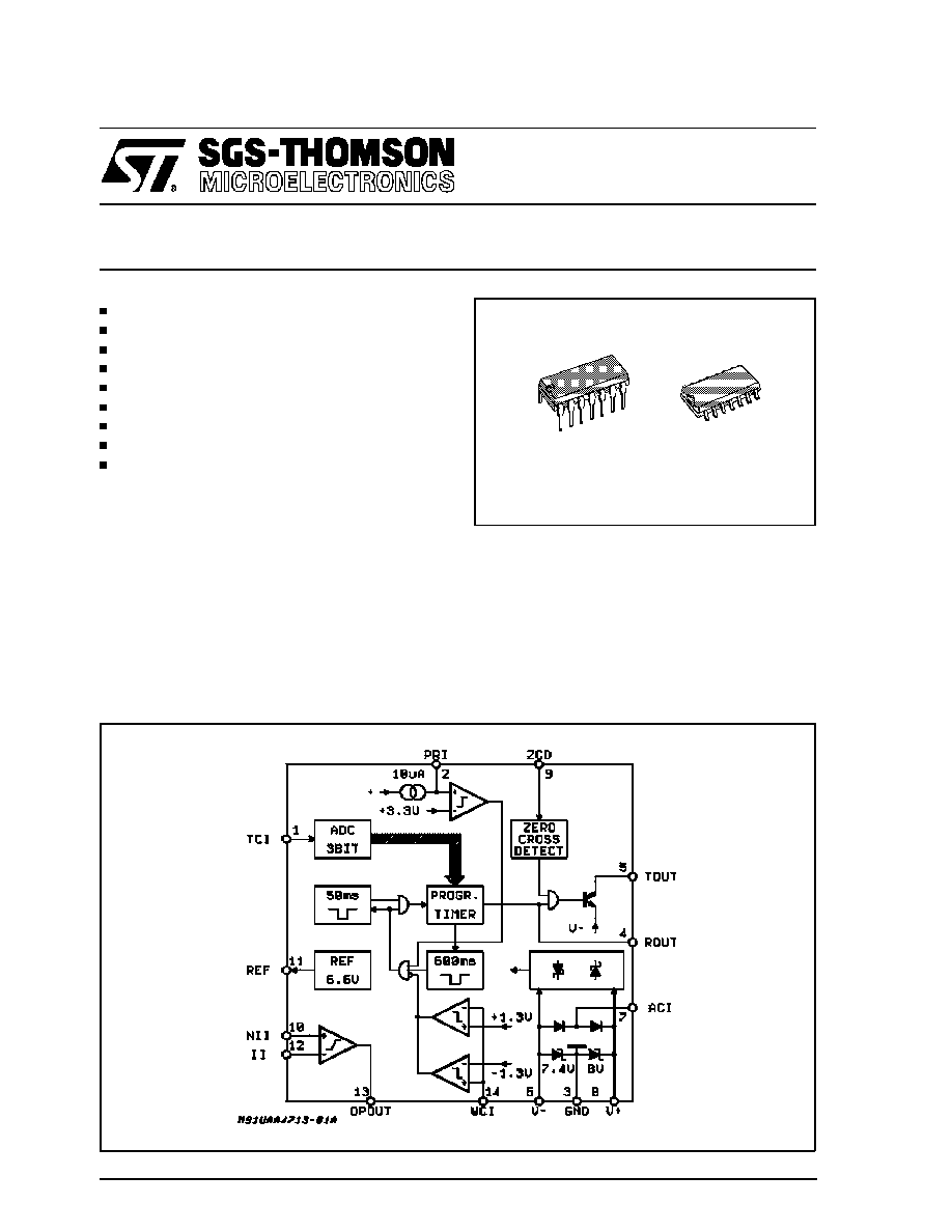
DESCRIPTION
The UAA4713 is a monolithic integrated circuit in-
tended to control triac or relay switch for AC-
mains timer applications.The device can be used
in a wide range of industrial and consumer appli-
cations as light control, automatic door opening
detector, fire alarm, fluid level control .
The circuit processes the output signal of an infra-
red pyroelectric detector which senses tempera-
ture changes caused by heat radiation of the hu-
man body.
If the sensor detects a temperature change, a
programmable timer will start and switch a lamp
or other loads to the mains.
A further input for a photo-resistive sensor allows
to program circuit operation depending on the
day-light intensity.
Internal circuits avoid false triggering of the exter-
nal actuators. (see functional diagram).
This is advanced information on a new product now in development or undergoing evaluation. Details are subject to change without notice.
December 1991
BLOCK DIAGRAM
DIP-14
SO-14
ORDERING NUMBERS:
UAA4713DP
UAA4713FP
1/14
FUNCTIONAL DIAGRAM
ABSOLUTE MAXIMUM RATINGS
Symbol
Parameter
Test Conditions
Unit
I7
AC Supply Current
60
mA
I7
Peak Current (T.P < 200
µ
s)
200
mA
I7
Sourge Current (not repetitive 10ms)
500
mA
I9
ZCD Max. Input Current
5
mA
V6-3
Negative Clamp Voltage
-9
V
V8-3
Positive Clamp Voltage
9.5
V
V14-3
Comp. Input Voltage
±
8
V
V10-12
Differential Input Voltage
±
8
V
Top
Operating Temperature
-25 to 85
∞
C
T
stg
,T
j
Junction and Storage Temperature
-40 to 150
∞
C
P
tot
Total Power Dissipation (T
j
= 85
∞
C)
650
mW
THERMAL DATA
Symbol
Parameter
Value
Unit
R
th j-amb
Thermal Resistance Junction-ambient
max
100
∞
C/W
UAA4713
2/14
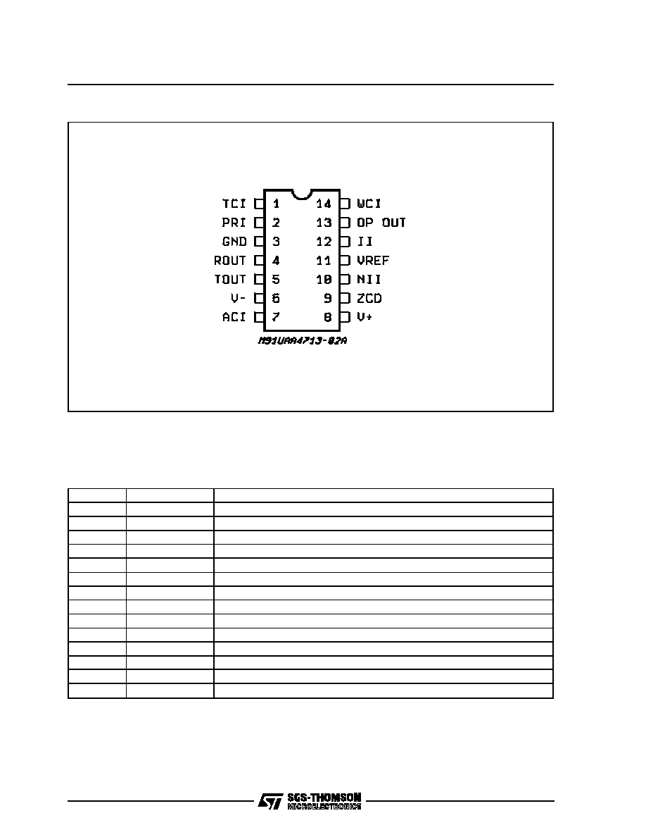
PIN CONNECTION (Top view)
Pin
Symbols
Functions
1
TCI
Time control Input
2
PRI
Photosensor comparator input
3
GND
Ground
4
R
OUT
Relay output
5
T
OUT
Triac output
6
V-
Negative clamp voltage
7
ACI
AC-input supply
8
V+
Positive clamp voltage
9
ZCD
Zero cross detector
10
NII
Non-invert input sensor amplifier
11
V
REF
Sensor reference voltage
12
II
Invert input sensor amplifier
13
OP OUT
Output sensor amplifier
14
WCI
Window comparator input
PIN FUNCTIONS
UAA4713
3/14

ELECTRICAL CHARACTERISTICS (I
S
= + 2mA to +10mA;T
amb
= 25
∞
C unless otherwise specified)
Symbol
Parameter
Test Condition
Pin
Min.
Typ.
Max.
Unit
I
S
Operative Supply Current
7
±
0.7
+ 15
mA
V-
Negative Clamping Voltage
±
I
S
= 0.7mA
6
-7.8
-7
V
V+
Positive Clamping Voltage
8
7.6
8.4
V
V
REF
Sensor Reference Voltage
I
REF
= 50
µ
A
I
REF
= 200
µ
A
11
6
5
6.6
7.2
7.2
V
V
I
ROUT
Output Current Relay Driver during on-time V
ROUT
= 0V
4
80
µ
A
V
R HIGH
Relay Driver Source
Saturation Voltage
I
R OUT
= 80
µ
A
4
2
V
I
R
Relay Sink Output Current
V
R OUT
= 0.4V during on-time
4
1
8
mA
I
TOUT
Triac Firing Current
5
50
65
mA
V
ZCD
Zero Cross Detector
Clamping Voltage
9
±
7.4
±
8
±
8.6
V
I
ZCD
Zero Cross Detector
Operating Current
9
1.6
10
µ
A
I
PRI
Photoresistor Source
Current
V
PRI
= 0V
2
6
10
14
µ
A
V
PRth
Photoresistor Threshold
Voltage
I
S
= 0.7mA
2
3
3.3
3.6
V
I
TCI
Timer Control Input Current
V
TCI
0 to V+
1
0
0.5
µ
A
t
TI M
On-Timer Counter Duration
(depends on the mains
frequency and on externally
adjustable Timer Control
Input Voltage) + 1/2 cicle
precision
V
TCI
14/4
50
60
Hz
11/12 V+
0
0
s
9/12
V+
4.48
3.73
s
7/12
V+
40
33.3
s
5/12
V+
81
67.5
s
3/12
V+
163
135.8
s
1/12
V+
327
272.5
s
0V (GND)
Continue
t
D
Delay Time Between
Window Comparator Input
and Timer Start
50Hz
14/4
40
50
60
ms
60Hz
33.3
41.6
50
ms
t
DR
Delay Time Between Timer
Stop to Retrigger
50Hz
14/4
500
ms
60Hz
600
ms
I
TOL
Triac Output Leakage Current V
TO
= 0V
5
10
µ
A
V
th WCI
Window Comparator T4
Pin 2 open
14/4
±
1.20
±
1.3
±
1.40
V
I
WCI
Window Comparator Input
Current
V
WCI
= -2V to + 2V
14
± 1
mA
OP. AMP.
R
I
Input Resistance
10/12
1
M
I
IO
Input Offset Current
10/12
25
nA
I
IB
Input Bias Current
10/12
1
µ
A
V
IO
Input Offset Voltage
10/12
- 10
+10
mV
V
CM
Common Mode Volt. Renge
10/12
- 4.5
5
V
V
O
Output Voltage Swing
13
±
4
±
5
V
I
O
Output Current
13
1.5
mA
I
SC
Output Short Circuit Current
13
3
mA
G
V
Large Signal Open Loop
Voltage Gain
R
L
= 10K
80
100
V
UAA4713
4/14
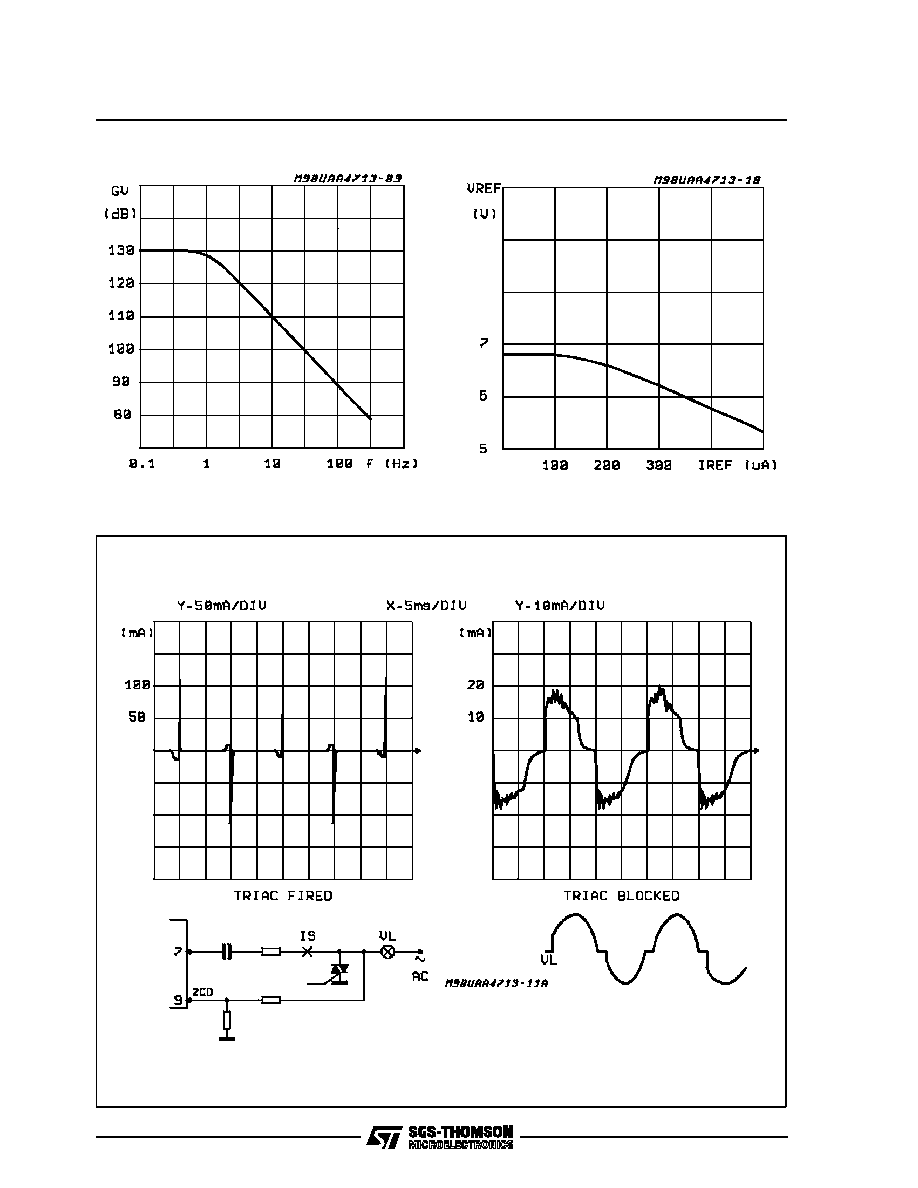
Figure 1: Open Loop Frequency Response
Figure 2: V
REF
versus I
REF
Figure 3: Supply Current
UAA4713
5/14
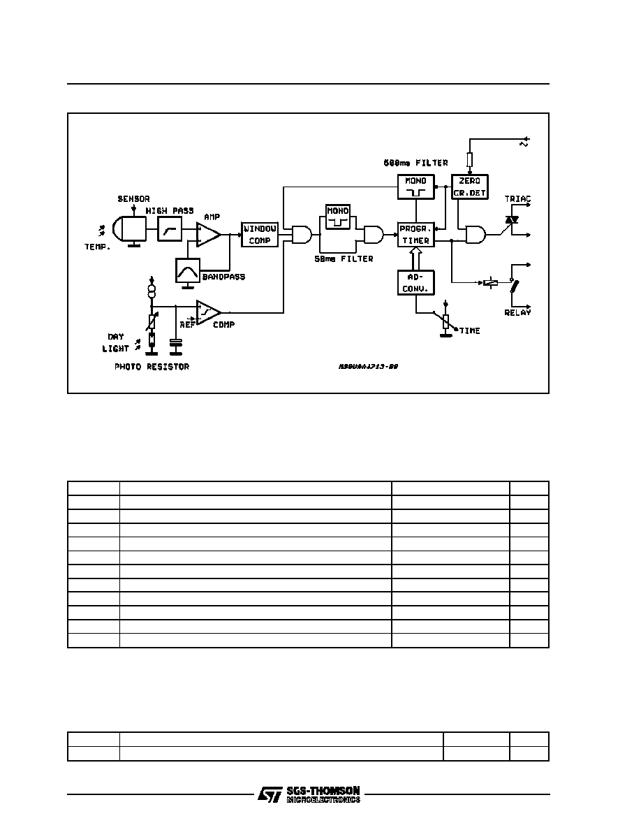
SYSTEM DESCRIPTION (see Functional Diagram)
If a heat source moves in front of the IR-detector,
the sensor delivers a quasi sinusoidal AC-signal
in the
µ
V to mV range. The operational amplifier
amplifies the sensor signal by 72dB.
To reject an unwanted signal, a band pass filter is
needed. If the AC-level at pin 14 exceeds the win-
dow comparator thresholds, the programmable
timer will start. To suppress short sensor signals,
a 50ms time filter is implemented between the
window comparator output and the programmable
timer. This function improves the noise immunity.
After the reset of the timer a second timer will pro-
vide a 600ms dead time to prevent retriggering of
the timer. This function avoids restarting of the
timer, when the turned off lamp temperature. de-
creases
The lamp switched by the triac can be located
close to the sensor.
To avoid circuit operation during day-time, a
photo resistor (LDR) senses the light intensity and
switches off the circuit. The capacitor at pin 2 pre-
vents circuit start-up during short shadow phases,
when a person passes by the sensor.
From the analog input pin 1 via the AD-converter
the on-time duration can be programmed in 7
steps (see t
TIM
table in the electical charac-
teristics). The timer is clocked by the mains fre-
quency.
Two outputs for various applications are avail-
able.
Pin 5 is the trigger output for triac gate.
Pin 4 output can be used to switch a relay or
other loads.
The zero crossing detector provides the firing
pulse for the triac at the right time, shortly after
the zero crossing of the AC-signal.
The RC-network at pin 7 supplies current to the
circuit via a double wave rectification which is pro-
vided by a split power supply. Due to the capaci-
tive energy transfer into pin 7, the circuit will also
be supplied with current if the triac is fired. A short
wire for circuit supply is not needed.
The circuit works similar to a simple two-terminal
switch and can be installed in parallel with ordi-
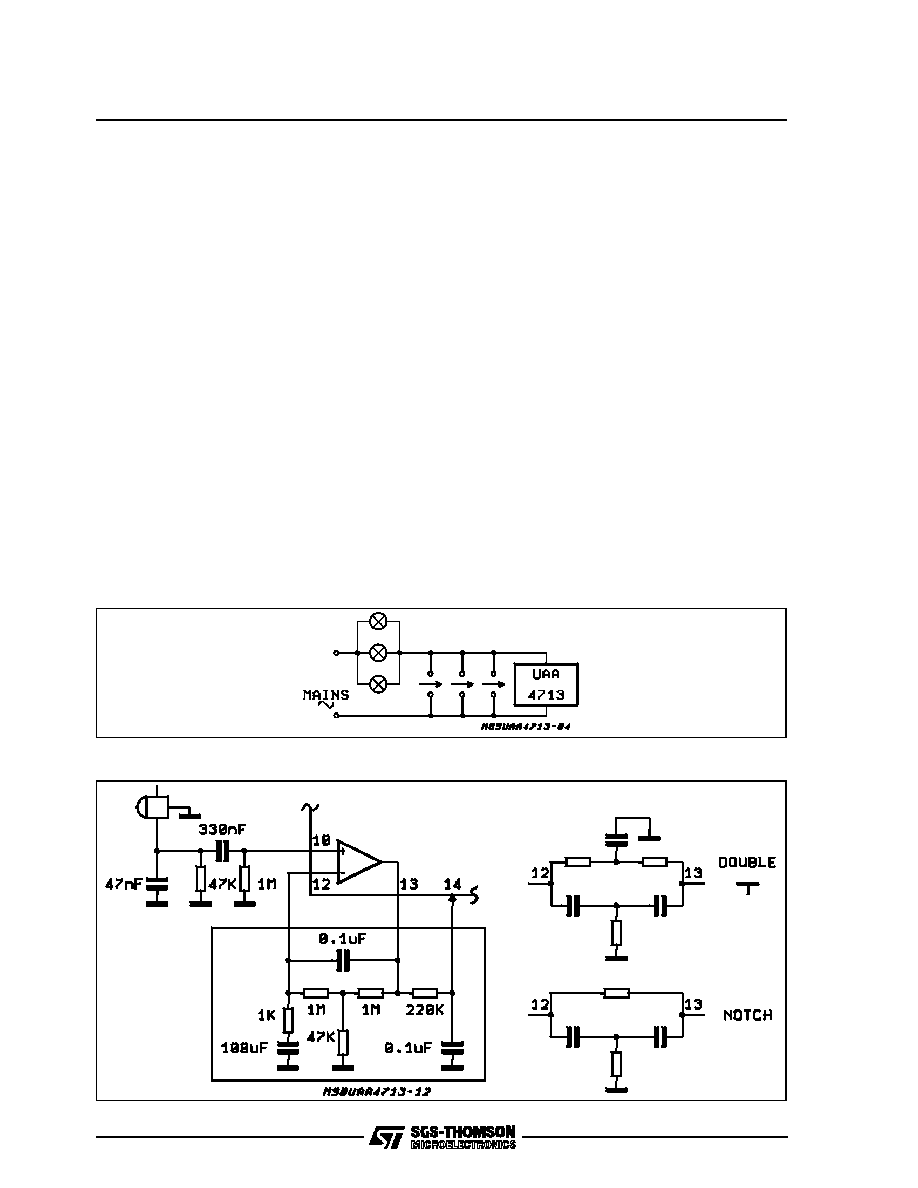
nary mechanical pulse switches (fig. 4).
After a short supply connection via an external
pulse switch, the circuit timer will also start with-
out a sensor signal.
Therefore the circuit can also be used as an ordi-
nary light timer without the IR-moving sensor fea-
ture.
Figure 4
Figure 5: Different Possible Filter Solutions
UAA4713
6/14
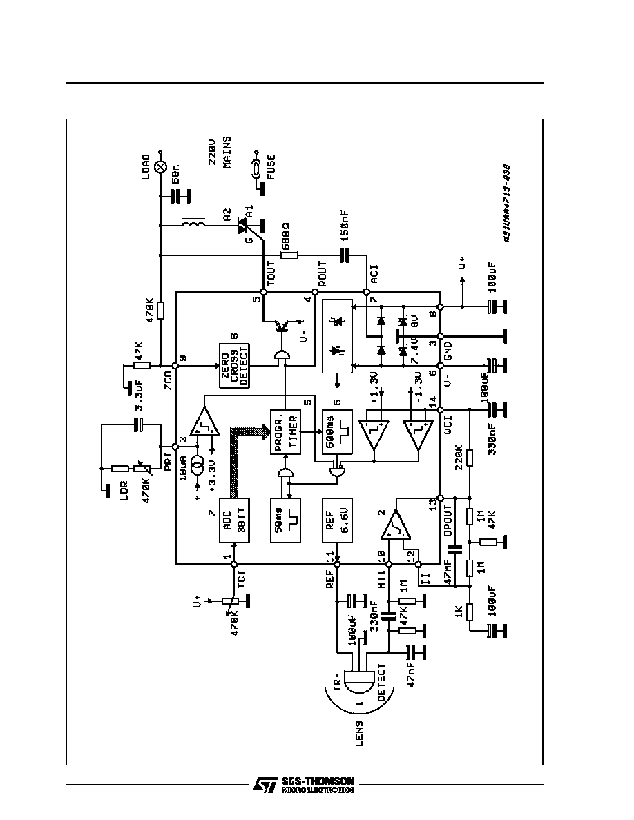
Figure 6: Triac Application
UAA4713
7/14
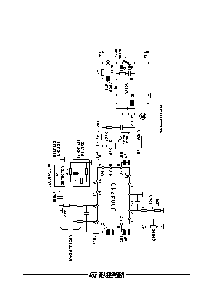
Figure 7: Relay Application
UAA4713
8/14
APPLICATION INFORMATION
1. HOW TO CHOOSE THE TRIAC ASSOCIATED
TO THE MOTION DETECTOR UAA4713
Analysis of the Triac Associated to the Motion
Detector UAA4713
Associated with the UAA4713, the Triac is de-
fined by the driver output stage (Triac output pin
5) and the characteristics of the load.
The Triac is consequently defined by:
1) The gate sensitivity
2) The surge current capability
3) The RMS Triac current
4) The blocking voltage capability
1) The gate sensitivity
The "Triggering gate current" is the parameter to
be taken into consideration. The I
GT
is given at
25
∞
C. as a maximum value required to trigger the
Triac.
ex. BTA06-600CW = I
GT max
(mA) = 35mA
The UAA4713 Triac output provides a current of
65mA typical.
I
Tout
= 65mA(Typ) = I
G
In order to control the Triac properly IG should be
greater than 1.5
x
I
GT
or
I
Tout
> 1.5 I
GT
For this reason it is suggested to use a snubber-
less Triac of the CW series (I
GT
< 35mA).
2) The surge current capability
In the Triac databook the surge current capability
of the Triac is given by the non repetitive surge
peak current:
I
TSM
ex. BTA06-600CW
I
TSM
at T
J initial
= 25
∞
C
t = 8.3mA: 63A
t = 10ms: 60A
The choice of the Triac is defined by the following
application parameters:
a)The starting performance, and the ratio of
the nominal resistance to the cold resis-
tance, KR
I
max
> KR
x
I
nominal x
2
b)The thermal fast fuse behaviour during
short-circuit condition.
(I
2
t) (Triac) > (I
2
t) (fuse)
To select the I
Tsm
(given as a minimum value) the
following table is suggested.
Mains: V
AC
(V)
240V
110V
Power (W)
600
1000
>1000
I
Tsm (min)
50
80
>100
I
Tsm (min)
80
120
>150
3) RMS Triac Current
The RMS Triac current I
TRMS
is defined by the
light power P:
I
TRMS
> 1. 25
x
P
x
V
AC
It depends also on the heat sink which has to limit
the junction temperature in the worse case condi-
tions (T
amb max
and I
TRMS)
.
With the snubberless triac I
TRMS
ranges from 6A
to 25A.
4) Blocking Voltage Capability
The maximum blocking voltage VD
RM
is defined
by the mains:
Country
Mains Voltage
(V) V
AC
V
DRM
(V)
EUROPE
240
600
USA
110
400
5) Conclusion:
Selector guide with the above parameters the op-
timal device selection for a given power to be
controlled is given in the following table:
LIGHT POWER
(W)
MAINS VOLTAGE V
AC
(V)
240
110
600
BTA 06 600 CW
BTA 08 400 CW
1,000
BTA 08 600 CW
BTA 12 400 CW
> 1,000
BTA X 600 CW
X = 10
X = 12
X = 16
BTA X 400 CW
X = 12
X = 16 (A)
Ref: High Performance Triacs that need no snub-
ber (DSTRIACBK/1088)
UAA4713
9/14
APPLICATION INFORMATION (continued)
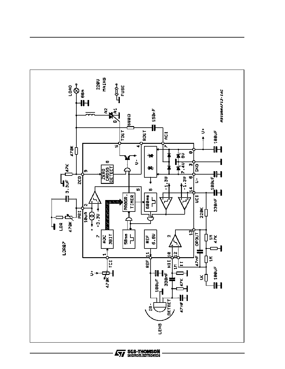
2. MOTION DETECTOR DEMO BOARD
This document allows the user to construct rap-
idly a Demo and Test Board for the UAA4713
Figure 8: Demo Board Diagram
UAA4713
10/14
Demo Board - Part List
QTY
DEVICE
DESCRIPTION
SUPPLIER
1
UAA4713DP OR UAA4713FP
INTEGRATED CIRCUIT
SGS-THOMSON
1
BTA06-600 (240V mains)
BTA08-400 (110V mains)
TRIAC
TRIAC
SGS-THOMSON
SGS-THOMSON
1
KRX10FL or
IRA - EI00S series
SENSOR WIT H FRESNEL LENS
Pyroelectic Infrared Sensor
PHILIPS COMPONENTS
MURATA
1
LDR07
PHOTORESISTOR
PHILIPS COMPONENTS
CAPACITORS
RESISTORS (0.25W)
QUANTITY
VALUE
QUANTITY
VALUE
4
100
µ
F/35V
3
1M
2
330nF
3
47k
2
47nF
1
680
1
4.7nF
1
1K
1
68nF 400V
1
470K
1
150nF 250V
1
220K
1
3.3
µ
F 35V
2 POTENTIOMETERS
500K
APPLICATION INFORMATION (continued)
Figure 9: Demo Board Photo IRA - E100S
UAA4713
11/14
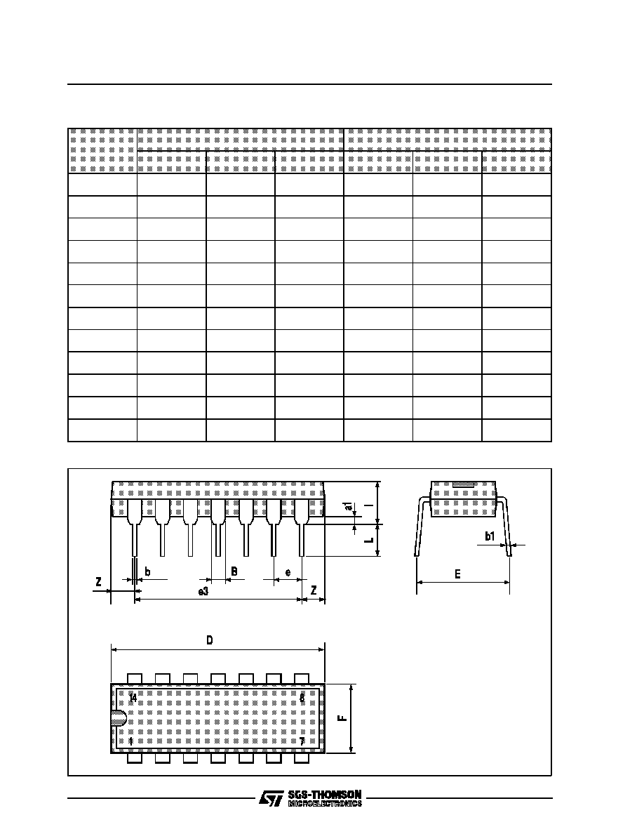
DIP14 PACKAGE MECHANICAL DATA
DIM.
mm
inch
MIN.
TYP.
MAX.
MIN.
TYP.
MAX.
a1
0.51
0.020
B
1.39
1.65
0.055
0.065
b
0.5
0.020
b1
0.25
0.010
D
20
0.787
E
8.5
0.335
e
2.54
0.100
e3
15.24
0.600
F
7.1
0.280
I
5.1
0.201
L
3.3
0.130
Z
1.27
2.54
0.050
0.100
UAA4713
12/14
SO14 PACKAGE MECHANICAL DATA
DIM.
mm
inch
MIN.
TYP.
MAX.
MIN.
TYP.
MAX.
A
1.75
0.069
a1
0.1
0.25
0.004
0.009
a2
1.6
0.063
b
0.35
0.46
0.014
0.018
b1
0.19
0.25
0.007
0.010
C
0.5
0.020
c1
45 (typ.)
D
8.55
8.75
0.336
0.344
E
5.8
6.2
0.228
0.244
e
1.27
0.050
e3
7.62
0.300
F
3.8
4.0
0.15
0.157
L
0.4
1.27
0.016
0.050
M
0.68
0.027
S
8 (max.)
UAA4713
13/14

Information furnished is believed to be accurate and reliable. However, SGS-THOMSON Microelectronics assumes no responsibility for the
consequences of use of such information nor for any infringement of patents or other rights of third parties which may result from its use. No
license is granted by implication or otherwise under any patent or patent rights of SGS-THOMSON Microelectronics. Specifications men-
tioned in this publication are subject to change without notice. This publication supersedes and replaces all information previously supplied.
SGS-THOMSON Microelectronics products are not authorized for use as critical components in life support devices or systems without ex-
press written approval of SGS-THOMSON Microelectronics.
©
1994 SGS-THOMSON Microelectronics - All Rights Reserved
SGS-THOMSON Microelectronics GROUP OF COMPANIES
Australia - Brazil - France - Germany - Hong Kong - Italy - Japan - Korea - Malaysia - Malta - Morocco - The Netherlands - Singapore -
Spain - Sweden - Switzerland - Taiwan - Thaliand - United Kingdom - U.S.A.
UAA4713
14/14