 | –≠–ª–µ–∫—Ç—Ä–æ–Ω–Ω—ã–π –∫–æ–º–ø–æ–Ω–µ–Ω—Ç: UC3843BN | –°–∫–∞—á–∞—Ç—å:  PDF PDF  ZIP ZIP |
UC2842B/3B/4B/5B
UC3842B/3B/4B/5B
March 1999
HIGH PERFORMANCE CURRENT MODE PWM CONTROLLER
.
TRIMMED OSCILLATOR FOR PRECISE FRE-
QUENCY CONTROL
.
OSCILLATOR FREQUENCY GUARANTEED
AT 250kHz
.
CURRENT MODE OPERATION TO 500kHz
.
AUTOMATIC FEED FORWARD COMPENSA-
TION
.
LATCHING PWM FOR CYCLE-BY-CYCLE
CURRENT LIMITING
.
INTERNALLY TRIMMED REFERENCE WITH
UNDERVOLTAGE LOCKOUT
.
HIGH CURRENT TOTEM POLE OUTPUT
.
UNDERVOLTAGE LOCKOUT WITH HYSTER-
ESIS
.
LOW START-UP AND OPERATING CURRENT
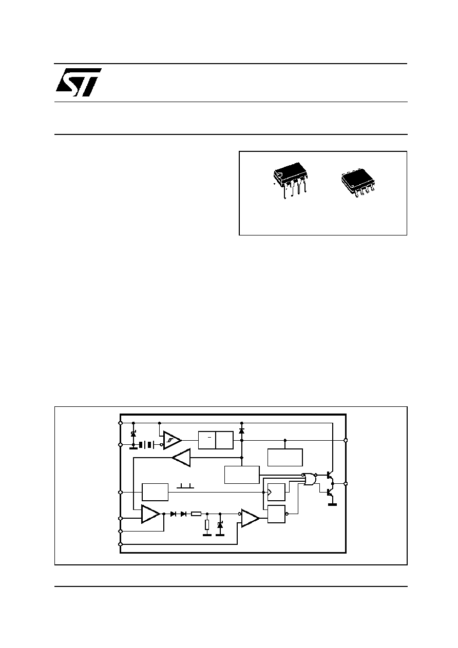
DESCRIPTION
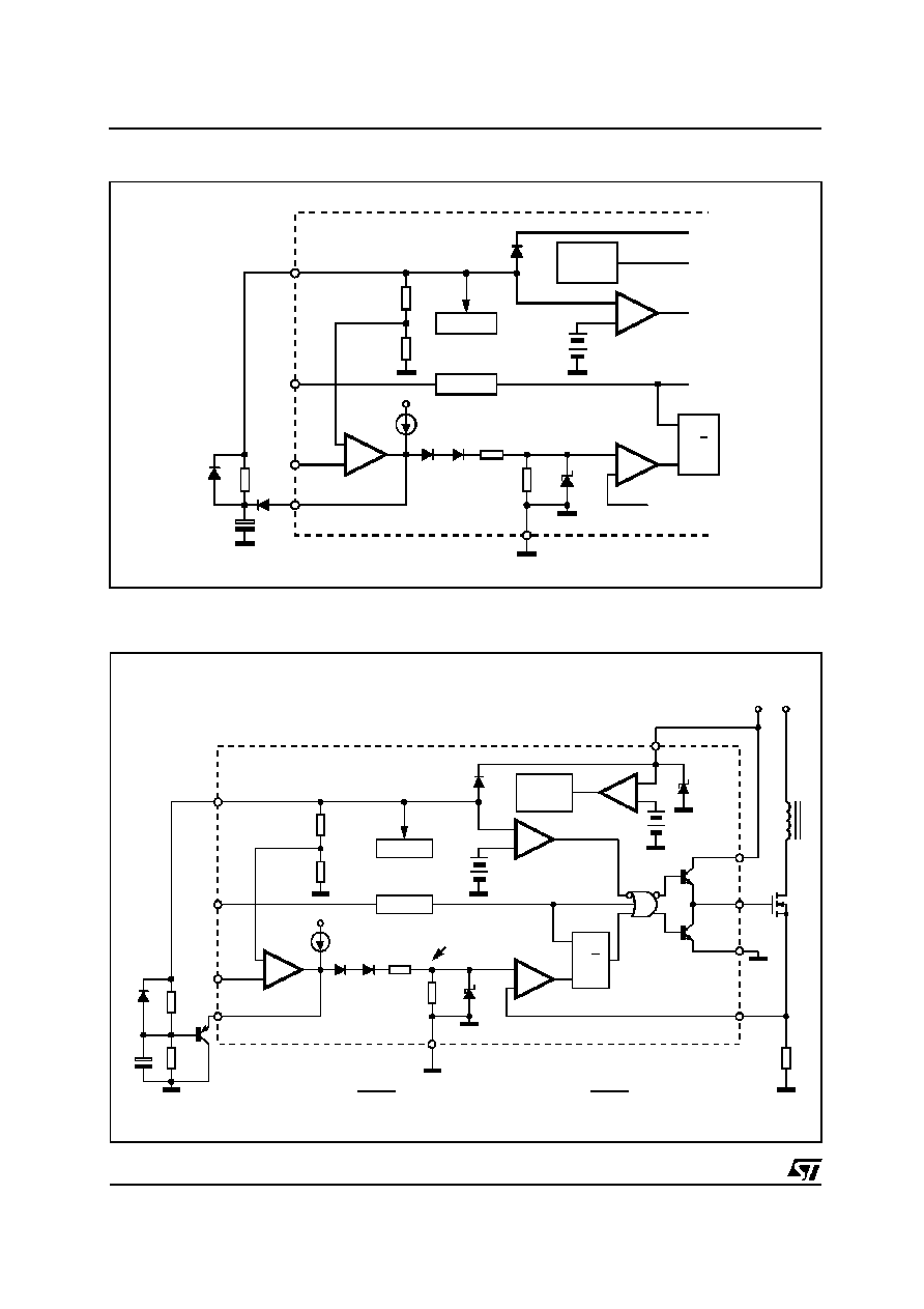
The UC384xB family of control ICs provides the nec-
essary features to implement off-line or DC to DC
fixed frequency current mode control schemes with
a minimal external parts count. Internally imple-
mented circuits include a trimmed oscillator for pre-
cise DUTY CYCLE CONTROL under voltage lock-
outfeaturingstart-up current less than0.5mA,a pre-
cision reference trimmed for accuracy at the error
amp input, logic to insure latched operation, a PWM
comparatorwhich alsoprovidescurrent limit control,
and a totem pole output stage designed to source
or sink high peakcurrent. The output stage, suitable
for driving N-Channel MOSFETs, is low in the off-
state.
Differences between members of this family are the
under-voltagelockout thresholds and maximum duty
cycle ranges. The UC3842B and UC3844B have
UVLO thresholds of 16V (on) and 10V (off), ideally
suitedoff-lineapplicationsThecorrespondingthresh-
oldsforthe UC3843BandUC3845Bare8.5 V and7.9
V. The UC3842B and UC3843B can operate to duty
cycles approaching 100%. A range of the zero to <
50 % is obtained by the UC3844B and UC3845B by
the addition of an internal toggle flip flop which blanks
the output off every other clock cycle.
BLOCK DIAGRAM (toggle flip flop used only in UC3844B and UC3845B)
UVLO
S/R
5V
REF
34V
INTERNAL
BIAS
VREF GOOD
LOGIC
2.50V
T
S
R
OSC
R
1V
CURRENT
SENSE
COMPARATOR
2R
+
-
PWM
LATCH
7
5
4
2
1
3
8
6
ERROR AMP.
Vi
GROUND
RT/CT
VFB
COMP
CURRENT
SENSE
VREF
5V 50mA
OUTPUT
D95IN331
Mini dip
Æ
SO8
UC3842B
1/15

* All voltages are with respect to pin 5, all currents are positive into the specified terminal.
PIN CONNECTION (top view)
COMP
V
FB
I
SENSE
R
T
/C
T
GROUND
OUTPUT
Vi
V
REF
1
3
2
4
6
5
7
8
D95IN332
Minidip/SO8
ORDERING NUMBERS
SO8
Minidip
UC2842BD1; UC3842BD1
UC2843BD1; UC3843BD1
UC2844BD1; UC3844BD1
UC2845BD1; UC3845BD1
UC2842BN; UC3842BN
UC2843BN; UC3843BN
UC2844BN; UC3844BN
UC2845BN; UC3845BN
ABSOLUTE MAXIMUM RATINGS
Symbol
Parameter
Valu e
Un it
V
i
Supply Voltage (low impedance source)
30
V
V
i
Supply Voltage (Ii < 30mA)
Self Limiting
I
O
Output Current
±
1
A
E
O
Output Energy (capacitive load)
5
µ
J
Analog Inputs (pins 2, 3)
≠ 0.3 to 5.5
V
Error Amplifier Output Sink Current
10
mA
P
tot
Power Dissipation at T
amb
25
∞
C (Minidip)
1.25
W
P
tot
Power Dissipation at Tamb
25
∞
C (SO8)
800
mW
T
stg
Storage Temperature Range
≠ 65 to 150
∞
C
T
J
Junction Operating Temperature
≠ 40 to 150
∞
C
T
L
Lead Temperature (soldering 10s)
300
∞
C
PIN FUNCTIONS
No
Function
Description
1
COMP
This pin is the Error Amplifier output and is made available for loop compensation.
2
V
FB
This is the inverting input of the Error Amplifier. It is normally connected to the switching
power supply output through a resistor divider.
3
I
SENSE
A voltage proportional to inductor current is connected to this input. The PWM uses this
information to terminate the output switch conduction.
4
R
T
/C
T
The oscillator frequency and maximum Output duty cycle are programmed by connecting
resistor R
T
to Vref and cpacitor C
T
to ground. Operation to 500kHz is possible.
5
GROUND
This pin is the combined control circuitry and power ground.
6
OUTPUT
This output directly drives the gate of a power MOSFET. Peak currents up to 1A are sourced
and sunk by this pin.
7
V
CC
This pin is the positive supply of the control IC.
8
V
ref
This is the reference output. It provides charging current for capacitor C
T
through resistor R
T
.
UC2842B/3B/4B/5B - UC3842B/3B/4B/5B
2/15

ELECTRICAL CHARACTERISTICS ( [note 1] Unless otherwise stated, these specifications apply for
-25 < T
amb
< 85
∞
C for UC284XB; 0 < T
amb
< 70
∞
C for UC384XB; V
i
= 15V (note 5); R
T
= 10K; C
T
= 3.3nF)
Symbo l
Parameter
T est Cond it ion s
UC284XB
UC384XB
Uni t
Min. Typ. Max. Min. Typ. Max.
REFERENCE SECTION
V
REF
Output Voltage
T
j
= 25
∞
C I
o
= 1mA
4.95
5.00
5.05
4.90
5.00
5.10
V
V
REF
Line Regulation
12V
V
i
25V
2
20
2
20
mV
V
REF
Load Regulation
1
I
o
20mA
3
25
3
25
mV
V
REF
/
T
Temperature Stability
(Note 2)
0.2
0.2
mV/
∞
C
Total Output Variation
Line, Load, Temperature
4.9
5.1
4.82
5.18
V
e
N
Output Noise Voltage
10Hz
f
10KHz T
j
= 25
∞
C
(note 2)
50
50
µ
V
Long Term Stability
T
amb
=
125
∞
C,
1000Hrs
(note 2)
5
25
5
25
mV
I
SC
Output Short Circuit
-30
-100 -180
-30
-100
-180
mA
OSCILLATOR SECTION
f
OSC
Frequency
T
j
= 25
∞
C
T
A
= T
low
to T
high
T
J
= 25
∞
C (R
T
= 6.2k, C
T
= 1nF)
49
48
225
52
≠
250
55
56
275
49
48
225
52
≠
250
55
56
275
KHz
KHz
KHz
f
OSC
/
V
Frequency Change with Volt. V
CC
= 12V to 25V
≠
0.2
1
≠
0.2
1
%
f
OSC
/
T
Frequency Change with Temp.
T
A
= T
low
to T
high
≠
1
≠
≠
0.5
≠
%
V
OSC
Oscillator Voltage Swing
(peak to peak)
≠
1.6
≠
≠
1.6
≠
V
I
dischg
Discharge Current (V
OSC
=2V) T
J
= 25
∞
C
T
A
= T
low
to T
high
7.8
7.5
8.3
≠
8.8
8.8
7.8
7.6
8.3
≠
8.8
8.8
mA
mA
ERROR AMP SECTION
V
2
Input Voltage
V
PIN1
= 2.5V
2.45
2.50
2.55
2.42
2.50
2.58
V
I
b
Input Bias Current
V
FB
= 5V
-0.1
-1
-0.1
-2
µ
A
A
VOL
2V
V
o
4V
65
90
65
90
dB
BW
Unity Gain Bandwidth
T
J
= 25
∞
C
0.7
1
0.7
1
MHz
PSRR
Power Supply Rejec. Ratio
12V
V
i
25V
60
70
60
70
dB
I
o
Output Sink Current
V
PIN2
= 2.7V
V
PIN1
= 1.1V
2
12
2
12
mA
I
o
Output Source Current
V
PIN2
= 2.3V V
PIN1
= 5V
-0.5
-1
-0.5
-1
mA
V
OUT
High
V
PIN2
= 2.3V;
R
L
= 15K
to Ground
5
6.2
5
6.2
V
V
OUT
Low
V
PIN2
= 2.7V;
R
L
= 15K
to Pin 8
0.8
1.1
0.8
1.1
V
CURRENT SENSE SECTION
G
V
Gain
(note 3 & 4)
2.85
3
3.15
2.85
3
3.15
V/V
V
3
Maximum Input Signal
V
PIN1
= 5V (note 3)
0.9
1
1.1
0.9
1
1.1
V
SVR
Supply Voltage Rejection
12
V
i
25V (note 3)
70
70
dB
I
b
Input Bias Current
-2
-10
-2
-10
µ
A
Delay to Output
150
300
150
300
ns
THERMAL DATA
Symbo l
Descri ption
Minid ip
SO 8
Unit
R
th j-amb
Thermal Resistance Junction-ambient.
max.
100
150
∞
C/W
UC2842B/3B/4B/5B - UC3842B/3B/4B/5B
3/15

Notes :
1. Max package power dissipation limits must be respected; low duty cycle pulse techniques are used during test maintain T
j
as
close to T
amb
as possible.
2. These parameters, although guaranteed, are not 100% tested in production.
3. Parameter measured at trip point of latch with V
PIN2
= 0.
4. Gain defined as :
V
PIN1
A =
; 0
V
PIN3
0.8 V
V
PIN3
5. Adjust V
i
above the start threshold before setting at 15 V.
ELECTRICAL CHARACTERISTICS (continued)
Symbo l
Parameter
T est Cond iti ons
UC284XB
UC384XB
Un it
Min . Typ . Max. Mi n. T yp. Max.
OUTPUT SECTION
V
OL
Output Low Level
I
SINK
= 20mA
0.1
0.4
0.1
0.4
V
I
SINK
= 200mA
1.6
2.2
1.6
2.2
V
V
OH
Output High Level
I
SOURCE
= 20mA
13
13.5
13
13.5
V
I
SOURCE
= 200mA
12
13.5
12
13.5
V
V
OLS
UVLO Saturation
VCC = 6V; I
SINK
= 1mA
0.1
1.1
0.1
1.1
V
t
r
Rise Time
T
j
= 25
∞
C
C
L
= 1nF (2)
50
150
50
150
ns
t
f
Fall Time
T
j
= 25
∞
C
C
L
= 1nF (2)
50
150
50
150
ns
UNDER-VOLTAGE LOCKOUT SECTION
Start Threshold
X842B/4B
15
16
17
14.5
16
17.5
V
X843B/5B
7.8
8.4
9.0
7.8
8.4
9.0
V
Min Operating Voltage
After Turn-on
X842B/4B
9
10
11
8.5
10
11.5
V
X843B/5B
7.0
7.6
8.2
7.0
7.6
8.2
V
PWM SECTION
Maximum Duty Cycle
X842B/3B
94
96
100
94
96
100
%
X844B/5B
47
48
50
47
48
50
%
Minimum Duty Cycle
0
0
%
TOTAL STANDBY CURRENT
I
st
Start-up Current
V
i
= 6.5V for UCX843B/45B
0.3
0.5
0.3
0.5
mA
V
i
= 14V for UCX842B/44B
0.3
0.5
0.3
0.5
mA
I
i
Operating Supply Current
V
PIN2
= V
PIN3
= 0V
12
17
12
17
mA
V
iz
Zener Voltage
I
i
= 25mA
30
36
30
36
V
UC2842B/3B/4B/5B - UC3842B/3B/4B/5B
4/15

Figure 1: Open Loop Test Circuit.
R
T
A
2N2222
4.7K
1K
ERROR AMP.
ADJUST
4.7K
5K
I
SENSE
ADJUST
100K
COMP
V
FB
I
SENSE
R
T
/C
T
1
2
3
4
C
T
7
6
5
8
V
REF
V
i
OUTPUT
GROUND
0.1
µ
F
0.1
µ
F
V
REF
V
i
OUTPUT
GROUND
1W
1K
D95IN343
High peak currents associated with capacitive loads
necessitate careful grounding techniques. Timing
and bypass capacitors should be connected close
to pin 5 in a single point ground. The transistor and
5 K
potentiometerareusedto samplethe oscillator
waveform and apply an adjustable ramp to pin 3.
10K
20K
30K
50K
100K
200K
300K
500K
fOSC(KHz)
1
2
5
10
20
50
D95IN333
C
T
=10nF
C
T
=5nF
C
T
=2nF
C
T
=1nF
C
T
=500pF
C
T
=200pF
C
T
=100pF
V
i
=15V
T
A
=25
∞
C
RT
(K
)
0.8
Figure 2: Timing Resistor vs. Oscillator Fre-
quency
10K
20K
30K
50K
100K
200K
300K
500K
fOSC(KHz)
1
2
3
5
10
20
30
50
%
C
T
=10nF
C
T
=5nF
C
T
=2nF
C
T
=1nF
C
T
=500pF
C
T
=200pF
C
T
=100pF
D95IN334
V
i
=15V
T
A
=25
∞
C
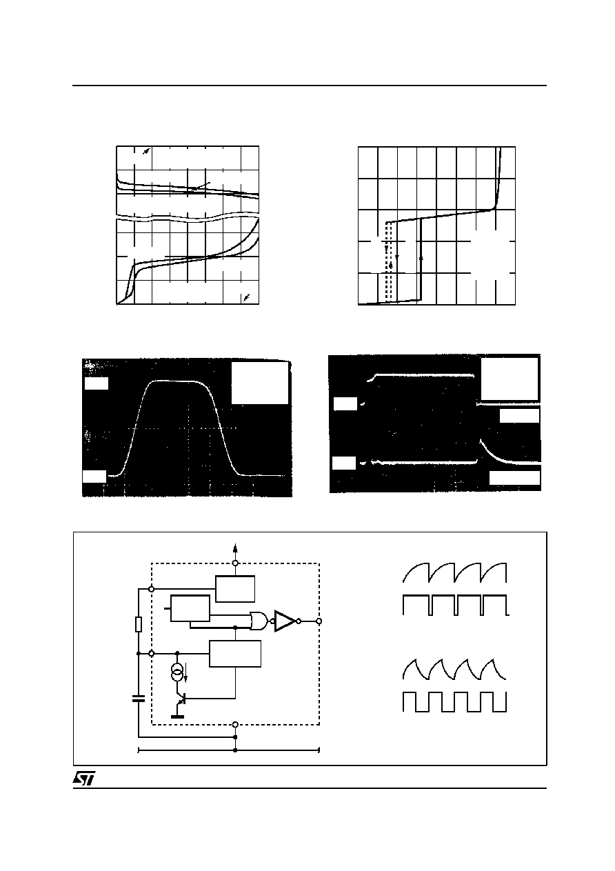
Figure 3: Output Dead-Time vs. Oscillator Fre-
quency
UC2842B
UC2842B/3B/4B/5B - UC3842B/3B/4B/5B
5/15

-55
-25
0
25
50
75
100 T
A
(
∞
C)
7.0
7.5
8.0
8.5
I
dischg
(mA)
D95IN335
V
i
=15V
V
OSC
=2V
Figure 4: Oscillator Discharge Current vs. Tem-
perature.
1
2
3
5
40
50
60
70
80
90
D
max
(%)
0.8
R
T
(K
)
D95IN336
V
i
=15V
C
T
=3.3nF
T
A
=25
∞
C
I
dischg
=7.5mA
I
dischg
=8.8mA
Figure 5: Maximum Output Duty Cycle vs. Tim-
ing Resistor.
10
100
1K
10K
100K
1M
f(Hz)
-20
0
20
40
60
80
(dB)
180
150
120
90
60
30
D95IN337
V
i
=15V
V
O
=2V to 4V
R
L
=100K
T
A
=25
∞
C
Gain
Phase
Figure 6: Error Amp Open-Loop Gain and
Phase vs. Frequency.
0
2
4
6
V
O
(V)
0.0
0.2
0.4
0.6
0.8
1.0
V
th
(V)
D95IN338
V
i
=15V
T
A
=-40
∞
C
T
A
=125
∞
C
T
A
=25
∞
C
Figure 7: Current Sense Input Threshold vs. Er-
ror Amp Output Voltage.
0
20
40
60
80
100 I
ref
(mA)
D95IN339
0
10
20
30
40
50
60
V
i
=15V
T
A
=-40
∞
C
T
A
=125
∞
C
T
A
=25
∞
C
Figure 8: Reference Voltage Change vs.
Source Current.
-55
-25
0
25
50
75
100 T
A
(
∞
C)
D95IN340
50
60
70
80
90
100
I
SC
(mA)
V
i
=15V
R
L
0.1
Figure 9: Reference Short Circuit Current vs.
Temperature.
UC2842B/3B/4B/5B - UC3842B/3B/4B/5B
6/15
0
200
400
600
I
O
(mA)
0
1
2
3
-2
-1
V
sat
(V)
D95IN341
V
i
=15V
80
µ
s Pulsed Load 120Hz Rate
T
A
=-40
∞
C
T
A
=25
∞
C
V
i
T
A
=-40
∞
C
T
A
=25
∞
C
GND
Sink Saturation
(Load to V
i
)
Source Saturation
(Load to Ground)
Figure 10: Output Saturation Voltagevs. Load
Current.
0
10
20
30
V
i
(V)
0
5
10
15
20
I
i
(mA)
UCX843/45
UCX842/44
R
T
=10K
C
T
=3.3nF
V
FB
=0V
I
Sense
=0V
T
A
=25
∞
C
D95IN342
Figure 11: Supply Current vs. Supply Voltage.
Figure 12: Output Waveform.
Figure 13: Output Cross Conduction
5V REG
OSCILLATOR
PWM
CLOCK
8
4
5
6
R
T
C
T
GND
OUTPUT
7
V
i
I
D
CT
OUTPUT
LARGE R
T
/SMALL C
T
CT
OUTPUT
SMALL R
T
/LARGE C
T
D95IN344
Figure 14: Oscillator and Output Waveforms.
V
i
=15V
C
L
= 1.0nF
T
A
= 25
∞
C
90%
10%
50ns/DIV
V
i
=30V
C
L
= 15pF
T
A
= 25
∞
C
V
O
I
CC
100ns/DIV
100mA/DIV
20V/DIV
UC2842B/3B/4B/5B - UC3842B/3B/4B/5B
7/15

Figure 15 : Error Amp Configuration.
Z
i
Z
f
1mA
2
1
V
FB
COMP
2.5V
D95IN345
+
-
Figure 16 : Under Voltage Lockout.
UC3842B
UC3844B
UC3843B
UC3845B
16V
8.4V
10V
7.6V
V
ON
V
OFF
V
i
ON/OFF COMMAND
TO REST OF IC
7
<0.5mA
<17mA
I
CC
V
CC
V
OFF
V
ON
D95IN346
Figure 17 : Current Sense Circuit .
ERROR
AMPL.
2R
R
1V
CURRENT
SENSE
COMPARATOR
1
CURRENT
SENSE
COMP
C
R
S
R
3
5
GND
I
S
D95IN347
Peak current (i
s
) is determined by the formula
1.0 V
I
S max
R
S
A small RC filter may be required to suppress switch transients.
During UVLO, the Output is low
UC2842B/3B/4B/5B - UC3842B/3B/4B/5B
8/15
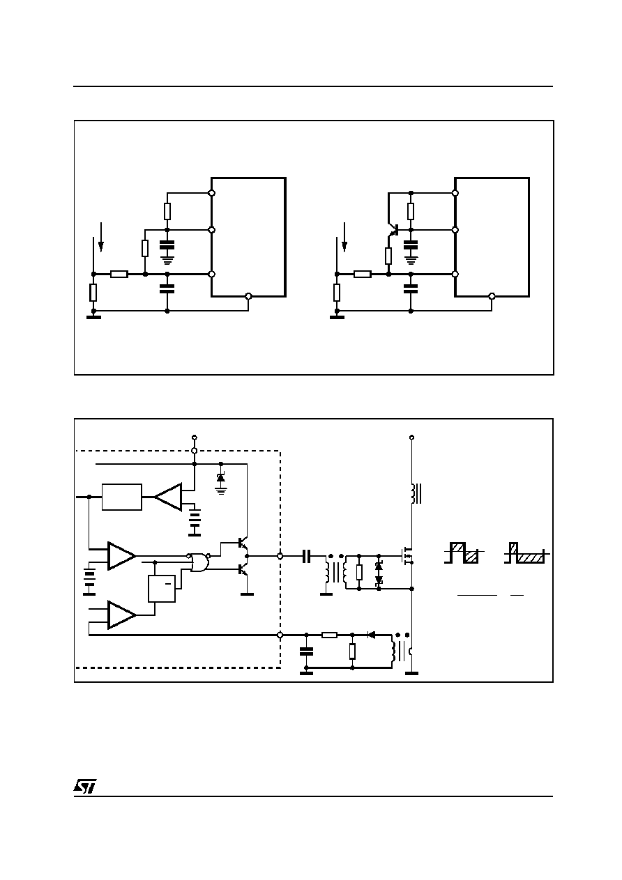
Figure 18 : Slope Compensation Techniques.
R
S
R
1
I
S
R
SLOPE
C
T
R
T
V
REG
8
R
T
/C
T
I
SENSE
4
3
5
GND
R
S
R
1
I
S
R
SLOPE
C
T
R
T
V
REG
8
R
T
/C
T
I
SENSE
4
3
5
GND
D95IN348
Figure 19 : Isolated MOSFET Drive and Current Transformer Sensing.
7
6
COMP/LATCH
ISOLATION
BOUNDARY
D95IN349
5.0Vref
V
CC
+
-
+
-
Q
S
R
+
-
3
R
R
S
N
S
C
V
in
Q1
N
P
V
GS
Waveforms
+
0
+
0
-
-
50% DC
25% DC
I
pk
=
V
(pin 1)
-1.4
3R
S
N
S
N
P
( )
UC3842B
UC3842B
UC2842B/3B/4B/5B - UC3842B/3B/4B/5B
9/15
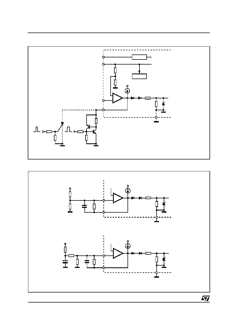
Figure 20 : Latched Shutdown.
D95IN350
BIAS
+
-
EA
R
+
OSC
2N
3905
2N
3903
1mA
R
R
2R
1
2
8
4
SCR must be selected for a holding current of less than 0.5mA at T
A(min)
.
The simple two transistor circuit can be used in place of the SCR as shown. All resistors are 10K.
5
D95IN351
+
-
EA
R
i
+
1mA
R
d
R
2R
5
C
f
R
f
1
2
From V
O
2.5V
+
-
EA
R
P
+
1mA
R
d
R
2R
5
C
f
R
f
1
2
From V
O
2.5V
Error Amp compensation circuit for stabilizing any current-mode topology except
for boost and flyback converters operating with continuous inductor current.
C
P
R
i
Error Amp compensation circuit for stabilizing current-mode boost and flyback
topologies operating with continuous inductor current.
Figure 21: Error Amplifier Compensation
UC2842B/3B/4B/5B - UC3842B/3B/4B/5B
10/15

D95IN353
+
-
+
R
A
1
7
f =
R
BIAS
OSC
C
6
V
REF
R
R
B
+
-
+
-
EA
R
2R
R
S
Q
8
4
5
2
3
5K
5K
5K
NE555
8
4
2
1
5
TO ADDITIONAL
UCX84XAs
1.44
(R
A
+ 2R
B
)C
D
max
=
R
B
R
A
+ 2R
B
Figure 23: External Duty Cycle Clamp and Multi Unit Synchronization.
D95IN352
+
-
EA
+
R
2R
5
R
T
1
2
EXTERNAL
SYNC INPUT
The diode clamp is required if the Sync amplitude is large enough to cause
the bottom side of C
T
to go more than 300mV below ground
R
BIAS
OSC
C
T
0.01
µ
F
47
4
8
V
REF
R
Figure 22: External Clock Synchronization.
UC2842B/3B/4B/5B - UC3842B/3B/4B/5B
11/15
D95IN354
+
R
BIAS
OSC
C
R
+
-
+
-
EA
R
2R
R
S
Q
8
4
2
1
5
1mA
1V
+
-
5V
ref
1M
Figure 24: Soft-Start Circuit
D95IN355
+
R
BIAS
OSC
C
R
+
-
+
-
EA
R
2R
R
S
Q
8
4
2
1
5
1mA
1V
+
-
5V
ref
R2
R1
V
Clamp
+
-
Comp/Latch
7
R
S
V
CC
Q1
V
in
7
6
5
BC109
V
CLAMP
=
∑
R
1
R
1
+ R
2
where 0 <V
CLAMP
<1V
I
pk(max)
=
V
CLAMP
R
S
Figure 25: Soft-Start and Error Amplifier Output Duty Cycle Clamp.
UC2842B/3B/4B/5B - UC3842B/3B/4B/5B
12/15
DIM.
mm
inch
MIN.
TYP.
MAX.
MIN.
TYP.
MAX.
A
1.75
0.069
a1
0.1
0.25
0.004
0.010
a2
1.65
0.065
a3
0.65
0.85
0.026
0.033
b
0.35
0.48
0.014
0.019
b1
0.19
0.25
0.007
0.010
C
0.25
0.5
0.010
0.020
c1
45
∞
(typ.)
D (1)
4.8
5.0
0.189
0.197
E
5.8
6.2
0.228
0.244
e
1.27
0.050
e3
3.81
0.150
F (1)
3.8
4.0
0.15
0.157
L
0.4
1.27
0.016
0.050
M
0.6
0.024
S
8
∞
(max.)
(1) D and F do not include mold flash or protrusions. Mold flash or
potrusions shall not exceed 0.15mm (.006inch).
SO8
OUTLINE AND
MECHANICAL DATA
UC2842B/3B/4B/5B - UC3842B/3B/4B/5B
13/15

Minidip
DIM.
mm
inch
MIN.
TYP.
MAX.
MIN.
TYP.
MAX.
A
3.32
0.131
a1
0.51
0.020
B
1.15
1.65
0.045
0.065
b
0.356
0.55
0.014
0.022
b1
0.204
0.304
0.008
0.012
D
10.92
0.430
E
7.95
9.75
0.313
0.384
e
2.54
0.100
e3
7.62
0.300
e4
7.62
0.300
F
6.6
0.260
I
5.08
0.200
L
3.18
3.81
0.125
0.150
Z
1.52
0.060
OUTLINE AND
MECHANICAL DATA
UC2842B/3B/4B/5B - UC3842B/3B/4B/5B
14/15

Information furnished is believed to be accurate and reliable. However, STMicroelectronics assumes no responsibility for the conse-
quences of use of such information nor for any infringement of patents or other rights of third parties which may result from its use. No
license is granted by implication or otherwise under any patent or patent rights of STMicroelectronics. Specification mentioned in this
publication are subject to change without notice. This publication supersedes and replaces all information previously supplied. STMi-
croelectronics products are not authorized for use as critical components in life support devices or systems without express written
approval of STMicroelectronics.
The ST logo is a registered trademark of STMicroelectronics
©
1999 STMicroelectronics ≠ Printed in Italy ≠ All Rights Reserved
STMicroelectronics GROUP OF COMPANIES
Australia - Brazil - Canada - China - France - Germany - Italy - Japan - Korea - Malaysia - Malta - Mexico - Morocco - The Netherlands -
Singapore - Spain - Sweden - Switzerland - Taiwan - Thailand - United Kingdom - U.S.A.
http://www.st.com
UC2842B/3B/4B/5B - UC3842B/3B/4B/5B
15/15