 | –≠–ª–µ–∫—Ç—Ä–æ–Ω–Ω—ã–π –∫–æ–º–ø–æ–Ω–µ–Ω—Ç: UC3845T | –°–∫–∞—á–∞—Ç—å:  PDF PDF  ZIP ZIP |
UC3842T UC3843T
UC3844T UC3845T
September 2001
HIGH PERFORMANCE CURRENT MODE PWM CONTROLLER
.
TRIMMED OSCILLATOR FOR PRECISE FRE-
QUENCY CONTROL
.
OSCILLATOR FREQUENCY GUARANTEED
AT 250kHz
.
CURRENT MODE OPERATION TO 500kHz
.
AUTOMATIC FEED FORWARD COMPENSA-
TION
.
LATCHING PWM FOR CYCLE-BY-CYCLE
CURRENT LIMITING
.
INTERNALLY TRIMMED REFERENCE WITH
UNDERVOLTAGE LOCKOUT
.
HIGH CURRENT TOTEM POLE OUTPUT
.
UNDERVOLTAGE LOCKOUT WITH HYSTER-
ESIS
.
LOW START-UP AND OPERATING CURRENT
DESCRIPTION
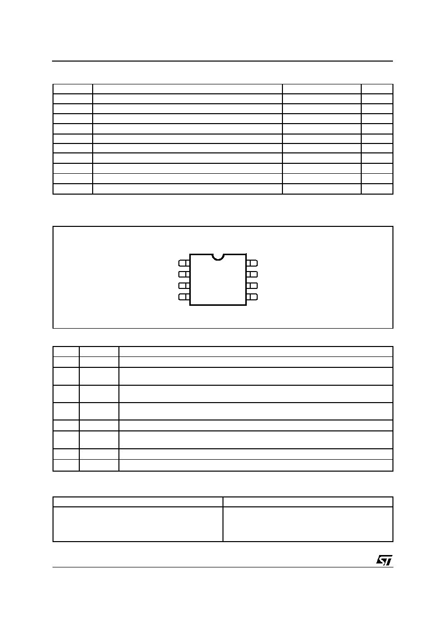
The UC384XT family of control ICs provides the
necessary features to implement off-line or DC to
DC fixed frequency current mode control schemes
with a minimal external parts count. Internally imple-
mented circuits include a trimmed oscillator for pre-
cise DUTY CYCLE CONTROL under voltage lock-
out featuring start-up current less than 0.5mA, a pre-
cision reference trimmed for accuracy at the error
amp input, logic to insure latched operation, a PWM
comparator which also provides current limit control,
and a totem pole output stage designed to source
or sink high peak current. The output stage, suitable
for driving N-Channel MOSFETs, is low in the off-
state.
Differences between members of this family are the
under-voltage lockout thresholds and maximum duty
cycle ranges. The UC3842T and UC3844T have
UVLO thresholds of 16V (on) and 10V (off), ideally
suited to off-line applications The corresponding
thresholds for the UC3843T and UC3845T are 8.5 V
and 7.9 V. The UC3842T and UC3843T can operate
to duty cycles approaching 100%. A range of zero to
< 50 % is obtained by the UC3844T and UC3845T by
the addition of an internal toggle flip flop which blanks
the output off every other clock cycle.
BLOCK DIAGRAM (toggle flip flop used only in UC3844T and UC3845T)
UVLO
S/R
5V
REF
34V
INTERNAL
BIAS
VREF GOOD
LOGIC
2.50V
T
S
R
OSC
R
1V
CURRENT
SENSE
COMPARATOR
2R
+
-
PWM
LATCH
7
5
4
2
1
3
8
6
ERROR AMP.
Vi
GROUND
RT/CT
VFB
COMP
CURRENT
SENSE
VREF
5V 50mA
OUTPUT
D95IN331
Minidip
Æ
SO8
1/15
* All voltages are with respect to pin 5, all currents are positive into the specified terminal.
PIN CONNECTION (top view)
COMP
V
FB
I
SENSE
R
T
/C
T
GROUND
OUTPUT
Vi
V
REF
1
3
2
4
6
5
7
8
D95IN332
Minidip/SO8
ORDERING NUMBERS
SO8
Minidip
UC3842TD
UC3843TD
UC3844TD
UC3845TD
UC3842TN
UC3843TN
UC3844TN
UC3845TN
ABSOLUTE MAXIMUM RATINGS
Symbol
Parameter
Value
Unit
V
i
Supply Voltage (low impedance source)
30
V
V
i
Supply Voltage (Ii < 30mA)
Self Limiting
I
O
Output Current
±
1
A
E
O
Output Energy (capacitive load)
5
µ
J
Analog Inputs (pins 2, 3)
≠ 0.3 to 5.5
V
Error Amplifier Output Sink Current
10
mA
P
tot
Power Dissipation at T
amb
25
∞
C (Minidip)
1.25
W
P
tot
Power Dissipation at Tamb
25
∞
C (SO8)
800
mW
T
stg
Storage Temperature Range
≠ 65 to 150
∞
C
T
L
Lead Temperature (soldering 10s)
300
∞
C
PIN FUNCTIONS
No
Function
Description
1
COMP
This pin is the Error Amplifier output and is made available for loop compensation.
2
V
FB
This is the inverting input of the Error Amplifier. It is normally connected to the switching
power supply output through a resistor divider.
3
I
SENSE
A voltage proportional to inductor current is connected to this input. The PWM uses this
information to terminate the output switch conduction.
4
R
T
/C
T
The oscillator frequency and maximum Output duty cycle are programmed by connecting
resistor R
T
to Vref and cpacitor C
T
to ground. Operation to 500kHz is possible.
5
GROUND
This pin is the combined control circuitry and power ground.
6
OUTPUT
This output directly drives the gate of a power MOSFET. Peak currents up to 1A are sourced
and sunk by this pin.
7
V
CC
This pin is the positive supply of the control IC.
8
V
ref
This is the reference output. It provides charging current for capacitor C
T
through resistor R
T
.
UC3842T - UC3843T - UC3844T - UC3845T
2/15
ELECTRICAL CHARACTERISTICS ( [note 1] Unless otherwise stated, these specifications apply for
0 < T
amb
< 105∞C; V
i
= 15V (note 5); R
T
= 10K; C
T
= 3.3nF)
Symbol
Parameter
Test Conditions
Value
Unit
Min.
Typ.
Max.
REFERENCE SECTION
V
REF
Line Regulation
12V
V
i
25V
2
20
mV
V
REF
Load Regulation
1
I
o
20mA
3
25
mV
V
REF
/
T
Temperature Stability
(Note 2)
0.2
mV/
∞
C
Total Output Variation
Line, Load, Temperature
4.85
5.15
V
e
N
Output Noise Voltage
10Hz
f
10KHz T
j
= 25
∞
C
(note 2)
50
µ
V
Long Term Stability
T
amb
= 125
∞
C, 1000Hrs (note 2)
5
25
mV
I
SC
Output Short Circuit
-30
-100
-180
mA
OSCILLATOR SECTION
f
OSC
Frequency
T
j
= 25
∞
C
T
A
= T
low
to T
high
T
J
= 25∞C (R
T
= 6.2k, C
T
= 1nF)
49
48
225
52
≠
250
55
56
275
KHz
KHz
KHz
f
OSC
/
V
Frequency Change with Volt.
V
CC
= 12V to 25V
≠
0.2
1
%
f
OSC
/
T
Frequency Change with Temp.
T
A
= T
low
to T
high
≠
1
≠
%
V
OSC
Oscillator Voltage Swing
(peak to peak)
≠
1.6
≠
V
I
dischg
Discharge Current (V
OSC
=2V)
T
A
= T
low
to T
high
7.3
≠
8.8
mA
ERROR AMP SECTION
V
2
Input Voltage
V
PIN1
= 2.5V
2.42
2.50
2.58
V
I
b
Input Bias Current
V
FB
= 5V
-0.1
-2
µ
A
A
VOL
2V
V
o
4V
65
90
dB
BW
Unity Gain Bandwidth
T
J
= 25∞C
0.7
1
MHz
PSRR
Power Supply Rejec. Ratio
12V
V
i
25V
60
70
dB
I
o
Output Sink Current
V
PIN2
= 2.7V V
PIN1
= 1.1V
2
12
mA
I
o
Output Source Current
V
PIN2
= 2.3V V
PIN1
= 5V
-0.5
-1
mA
V
OUT
High
V
PIN2
= 2.3V;
R
L
= 15K
to Ground
5
6.2
V
V
OUT
Low
V
PIN2
= 2.7V;
R
L
= 15K
to Pin 8
0.8
1.1
V
CURRENT SENSE SECTION
G
V
Gain
(note 3 & 4)
2.85
3
3.15
V/V
V
3
Maximum Input Signal
V
PIN1
= 5V (note 3)
0.9
1
1.1
V
SVR
Supply Voltage Rejection
12
V
i
25V (note 3)
70
dB
I
b
Input Bias Current
-2
-10
µ
A
Delay to Output
100
300
ns
THERMAL DATA
Symbol
Description
Minidip
SO8
Unit
R
th j-amb
Thermal Resistance Junction-ambient. max.
100
150
∞
C/W
U3842T - UC3843T - UC3844T - UC3845T
3/15
Notes :
1. Max package power dissipation limits must be respected; low duty cycle pulse techniques are used during test maintain T
j
as
close to T
amb
as possible.
2. These parameters, although guaranteed, are not 100% tested in production.
3. Parameter measured at trip point of latch with V
PIN2
= 0.
4. Gain defined as :
V
PIN1
A =
; 0
V
PIN3
0.8 V
V
PIN3
5. Adjust V
i
above the start threshold before setting at 15 V.
ELECTRICAL CHARACTERISTICS (continued)
Symbol
Parameter
Test Conditions
Value
Unit
Min.
Typ.
Max.
OUTPUT SECTION
V
OL
Output Low Level
I
SINK
= 20mA
0.1
0.4
V
I
SINK
= 200mA
1.6
2.2
V
V
OH
Output High Level
ISOURCE = 20mA
13
13.5
V
I
SOURCE
= 200mA
12
13.5
V
V
OLS
UVLO Saturation
VCC = 6V; I
SINK
= 1mA
0.1
1.1
V
t
r
Rise Time
T
j
= 25
∞
C C
L
= 1nF (2)
50
150
ns
t
f
Fall Time
T
j
= 25
∞
C C
L
= 1nF (2)
50
150
ns
UNDER-VOLTAGE LOCKOUT SECTION
Start Threshold
UC3842T/4T
15
16
17
V
UC3843T/5T
7.8
8.4
9.0
V
Min Operating Voltage
After Turn-on
UC3842T/4T
9
10
11
V
UC3843T/5T
7.0
7.6
8.2
V
PWM SECTION
Maximum Duty Cycle
UC3842T/3T
94
96
100
%
UC3844T/5T
47
48
50
%
Minimum Duty Cycle
0
%
TOTAL STANDBY CURRENT
I
st
Start-up Current
V
i
= 6.5V for UC3843T/45T
0.3
0.5
mA
V
i
= 14V for UC3842T/44T
0.3
0.5
mA
I
i
Operating Supply Current
V
PIN2
= V
PIN3
= 0V
12
17
mA
V
iz
Zener Voltage
I
i
= 25mA
30
36
V
UC3842T - UC3843T - UC3844T - UC3845T
4/15
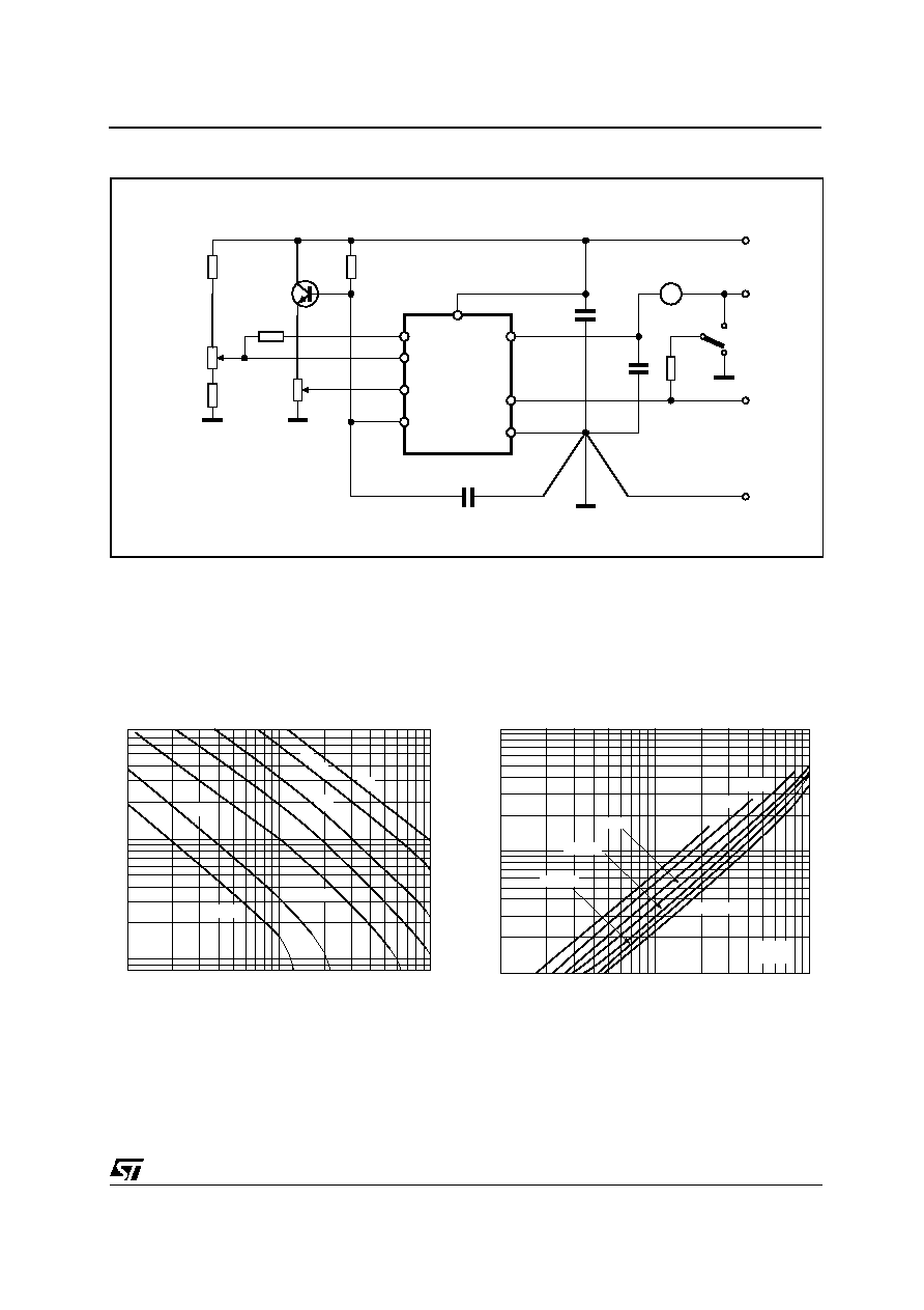
Figure 1: Open Loop Test Circuit.
R
T
A
2N2222
4.7K
1K
ERROR AMP.
ADJUST
4.7K
5K
I
SENSE
ADJUST
100K
COMP
V
FB
I
SENSE
R
T
/C
T
1
2
3
4
C
T
7
6
5
8
V
REF
V
i
OUTPUT
GROUND
0.1
µ
F
0.1
µ
F
V
REF
V
i
OUTPUT
GROUND
1W
1K
D95IN343
D.U.T.
High peak currents associated with capacitive loads
necessitate careful grounding techniques. Timing
and bypass capacitors should be connected close
to pin 5 in a single point ground. The transistor and
5 K
potentiometer are used to sample the oscillator
waveform and apply an adjustable ramp to pin 3.
10K
20K
30K
50K
100K
200K 300K
500K
f
OSC
(KHz)
1
2
5
10
20
50
D95IN333
C
T
=10nF
C
T
=5nF
C
T
=2nF
C
T
=1nF
C
T
=500pF
C
T
=200pF
C
T
=100pF
V
i
=15V
T
A
=25∞C
RT
(K
)
0.8
Figure 2: Timing Resistor vs. Oscillator Fre-
quency
10K
20K
30K
50K
100K
200K 300K
500K fOSC(KHz)
1
2
3
5
10
20
30
50
%
C
T
=10nF
C
T
=5nF
C
T
=2nF
C
T
=1nF
C
T
=500pF
C
T
=200pF
C
T
=100pF
D95IN334
V
i
=15V
T
A
=25∞C
Figure 3: Output Dead-Time vs. Oscillator Fre-
quency
U3842T - UC3843T - UC3844T - UC3845T
5/15