1/8
DATA BRIEFING
June 2002
Complete data available on
Data-on-Disc CD-ROM or at www.st.com .
µ
PSD3200 FAMILY
Flash Programmable System Device
with 8032 Microcontroller Core
FEATURES SUMMARY
s
The
µ
PSD3200 Family combines a Flash PSD
architecture with an 8032 microcontroller core
The
µ
PSD3200 Family of Flash PSDs features
dual banks of Flash memory, SRAM, general
purpose I/O and programmable logic, supervi-
sory functions and access via USB, I
2
C, ADC,
DDC and PWM channels, and an on-board
8032 microcontroller core, with two UARTs,
three 16-bit Timer/Counters and one External
Interrupt. As with other Flash PSD families, the
µ
PSD3200 Family is also in-system program-
mable (ISP) via a JTAG ISP interface.
s
Large 8 KByte SRAM with battery back-up
option
s
Dual bank Flash memories
≠ 128 KByte or 256 KByte main Flash memory
≠ 32 KByte secondary Flash memory
s
Content Security
≠ Block access to Flash memory
s
Programmable Decode PLD for flexible address
mapping of all memories.
s
High-speed clock standard 8032 core (12-cycle)
s
USB Interface (
µ
PSD3234A-40U6 only)
s
I
2
C interface for peripheral connections
s
Five Pulse Width Modulator (PWM) channels
s
Standalone Display Data Channel (DDC)
s
Six I/O ports with up to 50 I/O pins
s
3000 gate PLD with 16 macrocells
s
Supervisor functions
s
In-System Programming (ISP) via JTAG
s
Zero-Power Technology
s
Single Supply Voltage
≠ 4.5 to 5.5 V
≠ 3.0 to 3.6 V
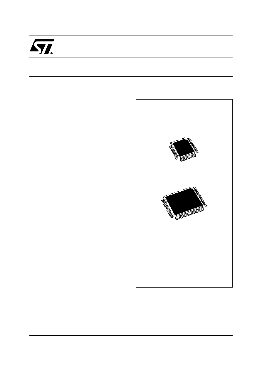
Figure 1. Packages
TQF P52 (T)
TQFP80 (U)

µ
PSD3200 FAMILY
2/8
SUMMARY DESCRIPTION
s
Dual bank Flash memories
≠ Concurrent operation, read from memory one
while erasing and writing the other. In-Appli-
cation Programming (IAP) for remote updates
≠ Large 128 KByte or 256 KByte main Flash
memory for application code, operating sys-
tems, or bit maps for graphic user interfaces
≠ Large 32 KByte secondary Flash memory di-
vided in small sectors. Eliminate external EE-
PROM with software EEPROM emulation
≠ Secondary Flash memory is large enough for
sophisticated communication protocol (USB)
during IAP while continuing critical system
tasks
s
Large SRAM with battery back-up option
≠ 8 KByte SRAM for RTOS, high-level languag-
es, communication buffers, and stacks
s
Programmable Decode PLD for flexible address
mapping of all memories
≠ Place individual Flash and SRAM sectors on
any address boundary
≠ Built-in page register breaks restrictive 8032
limit of 64 KByte address space
≠ Special register swaps Flash memory seg-
ments between 8032 "program" space and
"data" space for efficient In-Application Pro-
gramming
s
High-speed clock standard 8032 core (12-cycle)
≠ 40 MHz operation at 5 V, 24 MHz at 3.3 V
≠ Two UARTs with independent baud rate,
three 16-bit Timer/Counters and two External
Interrupts
s
USB Interface (
µ
PSD3234A-40U6 only)
≠ Supports USB 1.1 Slow Mode (1.5 Mbit/s)
≠ Control endpoint 0 and interrupt endpoints 1
and 2
s
I
2
C interface for peripheral connections
≠ Capable of master or slave operation
s
Five Pulse Width Modulator (PWM) channels
≠ Four 8-bit PWM units
≠ One 16-bit PWM unit
s
Standalone Display Data Channel (DDC)
≠ For use in monitor, projector, and TV applica-
tions
≠ Compliant with VESA standards DDC1 and
DDC2B
≠ Eliminate external DDC PROM
s
Six I/O ports with up to 50 I/O pins
≠ Multifunction I/O: GPIO, DDC, I
2
C, PWM,
PLD I/O, supervisor, and JTAG
≠ Eliminates need for external latches and logic
s
3000 gate PLD with 16 macrocells
≠ Create glue logic, state machines, delays,
etc.
≠ Eliminate external PALs, PLDs, and 74HCxx
≠ Simple PSDsoft Express software ...Free
s
Supervisor functions
≠ Generates reset upon low voltage or watch-
dog time-out. Eliminate external supervisor
device
≠ Reset In pin
s
In-System Programming (ISP) via JTAG
≠ Program entire chip in 10 - 25 seconds with
no involvement of 8032
≠ Allows efficient manufacturing, easy product
testing, and Just-In-Time inventory
≠ Eliminate sockets and pre-programmed parts
≠ Program with FlashLINK
TM
cable and any PC
s
Content Security
≠ Programmable Security Bit blocks access of
device programmers and readers
s
Zero-Power Technology
≠ Memories and PLD automatically reach
standby current between input changes
s
Packages
≠ 52-pin TQFP
≠ 80-pin TQFP: allows access to 8032 address/
data/control signals for connecting to external
peripherals
3/8
µ
PSD3200 FAMILY
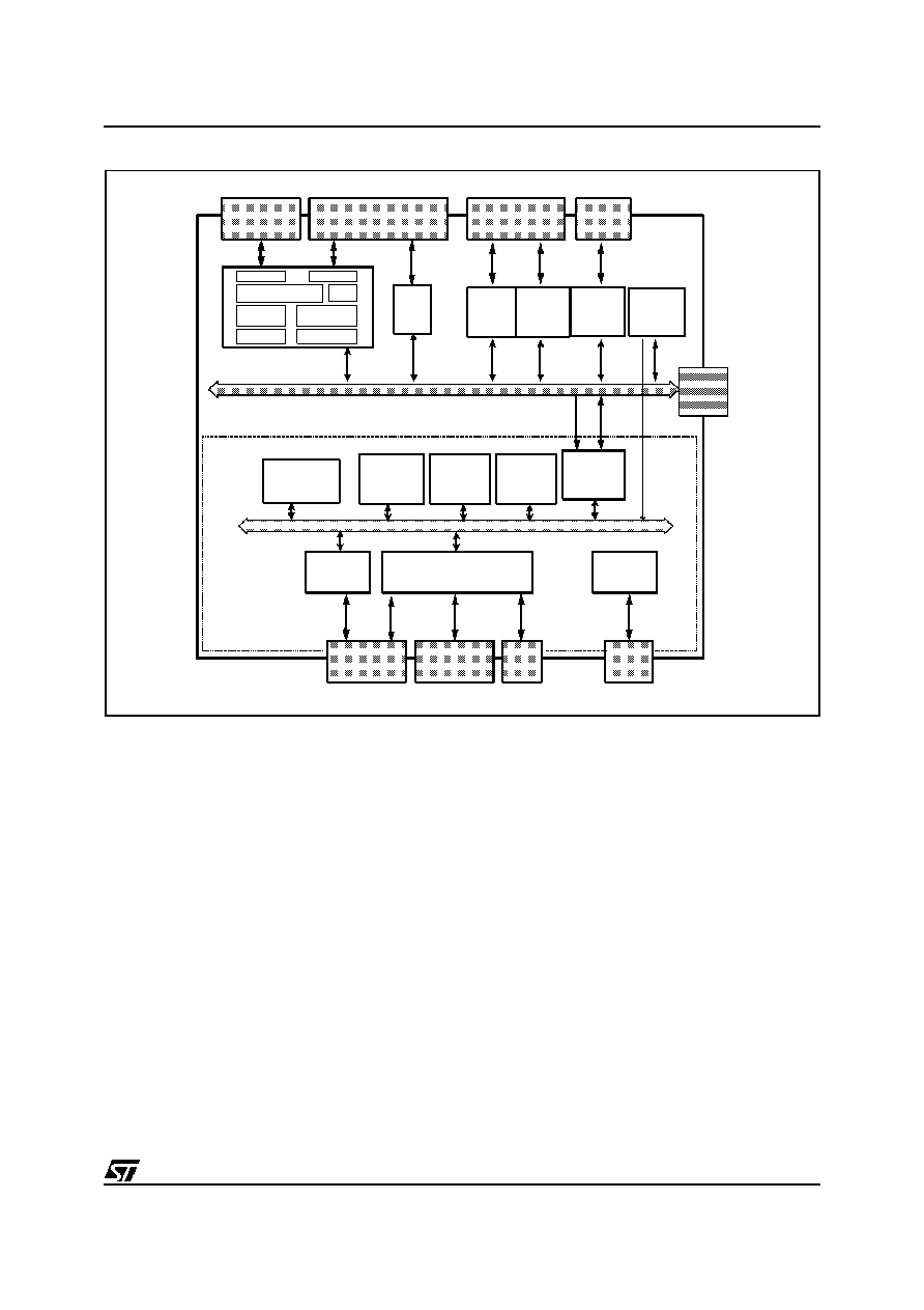
Figure 2.
µ
PSD3200 Family Functional Modules
AI06619
4
Channel
ADC
1Mb or 2Mb
Main Flash
Decode PLD
64Kb
SRAM
CPLD - 16 MACROCELLS
JTAG ISP
Port 1
Port 3
2 UARTS
Interrupt
3 Timer /
Counters
256 Byte SRAM
8051 Core
Port 3, UART,
Intr, Timers,I2C
PSD Internal Bus
8032 Internal Bus
USB
&
Transceiver
Port 1, Timers and
2nd UART and ADC
DDC
w/ 256 Byte
SRAM
PWM
5 Channels
Port 4 PWM
and DDC
Dedicated
USB Pins
Port A & B, PLD
I/O and GPIO
Port D
GPIO
Port C,
JTAG, PLD I/O
and GPIO
VCC, GND,
XTAL
256Kb
Secondary
Flash
Dedicated
Pins
I2C
Port 0, 2
Ext. Bus
Reset Logic
LVD & WDT
Bus Interface
Reset
D0-D7
A0-A15
RD,PSEN
WR,ALE
Page Register
PSD MODULE
MCU MODULE
µ
PSD3200 FAMILY
4/8
Table 1. 80-Pin Package Pin Description
Note: PSD Port A and MCU Address/Data bus are added for 80-pin device
Signal Name
In/Out
Function
Basic
Alternate
AD7-AD0
I/O
Multiplexed Address/Data bus
A11-A8
I/O
External Address Bus
RxD2-RxD1
I/O
General I/O port pins
UART Receive
TxD2-TxD1
I/O
UART Transmit
INT1-INT0
I/O
Interrupt inputs / timer gate controls
T2-T0
I/O
Counter inputs
SDA1-SDA2
I/O
I
2
C Bus serial data I/O / DDC interface
SCL1-SCL2
I/O
I
2
C Bus clock I/O
VSYNC
I/O
VSYNC input for DDC interface
T2EX
I/O
Timer 2 Trigger input
ADC3-ADC0
I/O
ADC Channels input
PWM4-PWM0
I/O
8-bit Pulse Width Modulation outputs
USB-, USB+
I/O
USB I/O
AVREF
O
Reference Voltage input for ADC
RD_
O
Read signal, external bus
WR_
O
Write signal, external bus
PSEN_
O
PSEN signal, external bus
ALE
O
Address Latch signal, external bus
RESET_
I
Active low reset input
XTAL1
I
Oscillator input pin for system clock
XTAL2
O
Oscillator output pin for system clock
PA7-PA0
I/O
General I/O port pins
1. PLD Macro-cell outputs
2. PLD inputs
3. Latched Address Out (A0-A7)
4. Peripheral I/O mode
PB7-PB0
I/O
General I/O port pins
1. PLD Macro-cell outputs
2. PLD inputs
3. Latched Address Out (A0-A7)
PC7-PC0
I/O
General I/O port pins
1. PLD Macro-cell outputs
2. PLD inputs
3. SRAM stand by voltage input (VSTBY)
4. JTAG Interface (TDI, TDO, TMS, TCK, TSTAT,
TERR)
5. SRAM battery-on indicator (PC4)
PD2-PD1
I/O
General I/O port pin
1. PLD I/O
2. Clock input to PLD and APD
3. Chip select to PSD Module

5/8
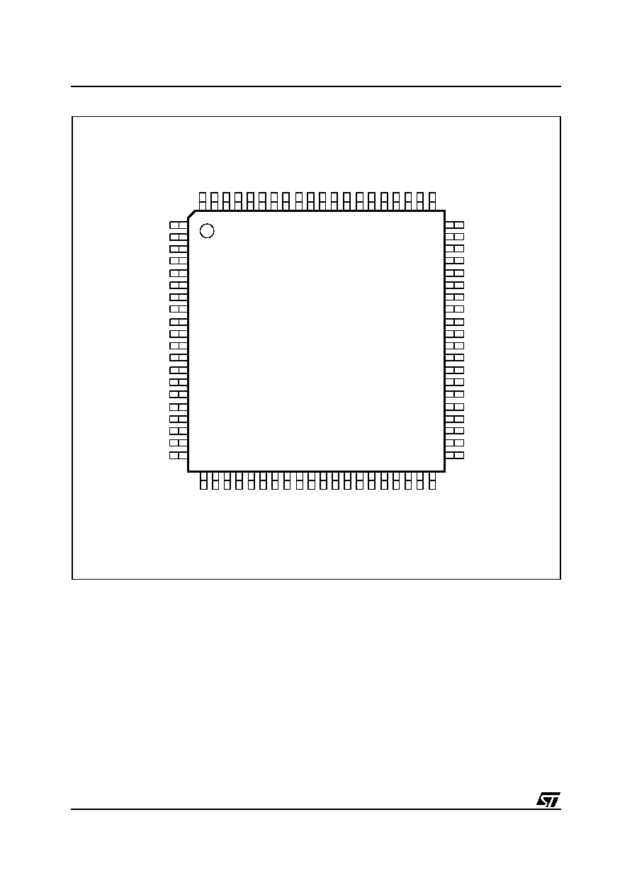
µ
PSD3200 FAMILY
Figure 3. TQFP52 Connections
Note: NC = Not Connected
PU = Pull-up resistor required (2k
for 3V devices, 7.5k
for 5V devices)
39 P1.5 / ADC1
38 P1.4 / ADC0
37 P1.3 / TXD1
36 P1.2 / RXD1
35 P1.1 / T2X
34 P1.0 / T2
33 V
CC
32 XTAL2
31 XTAL1
30 P3.7 / SCL1
29 P3.6 / SDA1
28 P3.5 / T1
27 P3.4 / T0
PD1
PC7
PC6
PC5
PU
PC4
NC
V
CC
GND
PC3
PC2
PC1
PC0
1
2
3
4
5
6
7
8
9
10
11
12
13
52
51
50
49
48
47
46
45
44
43
42
41
40
PB0
PB1
PB2
PB3
PB4
PB5
VREF
GND
RST-IN
PB6
PB7
ADC3
ADC2
14
15
16
17
18
19
20
21
22
23
24
25
26
P4.7
/
PWM4
P4.6
/
PWM3
P4.5
/
PWM2
P4.4
/
PWM1
P4.3
/
PWM0
GND
P4.2
/
DDC
VSYNC
P4.1
/
DDC
SCL
P4.0
/
DDC
SDA
P3.0
/
RXD
P3.1
/
TXD
P3.2
/
EXINT0
P3.3
/
EXINT1
AI05790B
µ
PSD3200 FAMILY
6/8
Figure 4. TQFP80 Connections
Note: 1. NC = Not Connected
2. USB- needs a pull-up resistor (see the description of the USB function)
60 P1.5 / ADC1
59 P1.4 / ADC0
58 P1.3 / TXD1
57 P2.3, A11
56 P1.2 / RXD1
55 P2.2, A10
54 P1.1 / T2X
53 P2.1, A9
52 P1.0 / T2
51 P2.0, A8
50 VCC
49 XTAL2
48 XTAL1
47 P0.7, AD7
46 P3.7 / SCL1
45 P0.6, AD6
44 P3.6 / SDA1
43 P0.5, AD5
42 P3.5 / T1
41 P0.4, AD4
PD2
P3.3 /EXINT1
PD1
PD0, ALE
PC7
PC6
PC5
USB-
PC4
USB+
NC
VCC
GND
PC3
PC2
PC1
NC
P4.7 / PWM4
P4.6 / PWM3
PC0
1
2
3
4
5
6
7
8
9
10
11
12
13
14
15
16
17
18
19
20
80
79
78
77
76
75
74
73
72
71
70
69
68
67
66
65
64
63
62
61
PB0
P3.2
/
EXINT0
PB1
P3.1
/
TXD
PB2
P3.0
/
RXD
PB3
PB4
PB5
NC
VREF
GND
RESET-IN
PB6
PB7
RD,
CNTL1
P1.7
/
ADC3
PSEN,
CNTL2
WR,
CNTL0
P1.6
/
ADC2
21
22
23
24
25
26
27
28
29
30
31
32
33
34
35
36
37
38
39
40
PA7
PA6
P4.5
/
PWM2
PA5
P4.4
/
PWM1
PA4
P4.3
/
PWM0
PA3
GND
P4.2
/
DCC
VSYNC
P4.1
/
DDC
SCL
PA2
P4.0
/
DDC
SDA
PA1
PA0
AD0,
P0.0
AD1,
P0.1
AD2,
P0.2
AD3,
P0.3
P3.4
/
T
0
AI05791

7/8
µ
PSD3200 FAMILY
PART NUMBERING
Table 2. Ordering Information Scheme
For a list of available options (speed, package,
etc.) or for further information on any aspect of this
device, please contact your nearest ST Sales Of-
fice.
Example:
uPSD 3
2
3
4
B
V
≠ 24 U
6
T
Device Type
uPSD = Microcontroller PSD
Family
3 = 8032 core
PLD Size
2 = 16 Macrocells
3 = 32 Macrocells
SRAM Size
1 = 16 Kbit
3 = 64 Kbit
5 = 256 Kbit
Main Flash Memory Size
3 = 1 Mbit
4 = 2 Mbit
5 = 4 Mbit
IP Mix
A = USB, I
2
C, PWM, DDC, ADC, (2) UARTs
Supervisor (Reset Out, Reset In, LVD, WD)
B = I
2
C, PWM, DDC, ADC, (2) UARTs
Supervisor (Reset Out, Reset In, LVD, WD)
Operating Voltage
blank = V
CC
= 4.5 to 5.5V
V = V
CC
= 3.0 to 3.6V
Speed
24 = 24 MHz
40 = 40 MHz
Package
T = 52-pin TQFP
U = 80-pin TQFP
Temperature Range
1 = 0 to 70
∞
C (commercial)
6 = ≠40 to 85
∞
C (industrial)
Optio n
T = Tape & Reel Packing

µ
PSD3200 FAMILY
8/8
Information furnished is believed to be accurate and reliable. However, STMicroelectronics assumes no responsibility for the consequences
of use of such information nor for any infringement of patents or other rights of third parties which may result from its use. No license is granted
by implication or otherwise under any patent or patent rights of STMicroelectronics. Specifications mentioned in this publication are subject
to change without notice. This publication supersedes and replaces all information previously supplied. STMi croelectronics products are not
authorized for use as critical components in lif e support devices or systems without express written approval of STMicroelectronics.
The ST logo is registered trademark of STMicroelectronics
All other names are the property of their respective owners
©
2002 STMicroelectronics - All Rights Reserved
STMicroelectronics group of companies
Australia - Brazil - Canada - China - Finland - France - Germany - Hong Kong -
India - Israel - Italy - Japan - Malaysia - Malta - Morocco - Singapore - Spain - Sweden - Switzerland - United Kingdom - United States.
www.st.com