 | –≠–ª–µ–∫—Ç—Ä–æ–Ω–Ω—ã–π –∫–æ–º–ø–æ–Ω–µ–Ω—Ç: UPSD3354D | –°–∫–∞—á–∞—Ç—å:  PDF PDF  ZIP ZIP |

1/129
PRELIMINARY DATA
September 2003
This is preliminary information on a new product now in development or undergoing evaluation. Details are subject to change without notice.
Rev. 1.2
uPSD33XX
uPSD33XX (Turbo Series)
Fast 8032 MCU With Programmable Logic
FEATURES SUMMARY
8-bit System On Chip for Embedded Control
The Turbo uPSD3300 Series combines a power-
ful, 8051-based microcontroller with a flexible
memory structure, programmable logic, and a rich
peripheral mix to form an ideal SOC for embedded
control. At it's core is a fast, 4-cycle 8032 MCU
with a 6-byte instruction prefetch queue and a 4-
entry, fully associative branching cache to maxi-
mize MCU performance, enabling smaller loops of
code to execute very quickly.
s
Fast Turbo 8032 MCU
s
Programmable Counter Array (PCA)
s
JTAG Debug and In-System Programming
s
Programmable Logic, General Purpose
s
Dual Flash Memories w/Memory Managment
≠ True READ-while-WRITE concurrent access
≠ Main Flash size: 64K, 128K, or 256K Bytes
≠ Secondary Flash size: 16K or 32K bytes
≠ 100,000 min erase cycles, 15 year retention
≠ On-chip programmable memory decode logic
s
SRAM
s
Peripheral Interfaces
s
Supervisor Functions
s
Content Security
s
Operating Range
≠ 3.3V applications: V
CC
= 3.3V ± 10%
≠ 5.0V applications: V
CC
: Both 5.0V ± 10% and
3.3V ± 10% sources are required.
≠ Temp: ≠40∞C to +85∞C (Industrial Range)
s
TQFP Packaging
≠ 52-pin (10x10mm)
≠ 80-pin (12x12mm)
Figure 1. 52-lead, Thin, Quad, Flat Package
Figure 2. 80-lead, Thin, Quad, Flat Package
TQFP52 (T)
TQFP80 (U)

uPSD33XX
2/129
TABLE OF CONTENTS
SUMMARY DESCRIPTION . . . . . . . . . . . . . . . . . . . . . . . . . . . . . . . . . . . . . . . . . . . . . . . . . . . . . . . . . . . 6
uPSD33XX HARDWARE DESCRIPTION. . . . . . . . . . . . . . . . . . . . . . . . . . . . . . . . . . . . . . . . . . . . . . . 13
MEMORY ORGANIZATION . . . . . . . . . . . . . . . . . . . . . . . . . . . . . . . . . . . . . . . . . . . . . . . . . . . . . . . . . 15
Internal Memory (MCU Module, Standard 8032 Memory: DATA, IDATA, SFR) . . . . . . . . . . . . 16
External Memory (PSD Module: Program memory, Data memory). . . . . . . . . . . . . . . . . . . . . . 16
8032 MCU CORE PERFORMANCE ENHANCEMENTS . . . . . . . . . . . . . . . . . . . . . . . . . . . . . . . . . . . 17
Pre-Fetch Queue (PFQ) and Branch Cache (BC) . . . . . . . . . . . . . . . . . . . . . . . . . . . . . . . . . . . . 19
PFQ Example, Multi-cycle Instructions . . . . . . . . . . . . . . . . . . . . . . . . . . . . . . . . . . . . . . . . . . . . 19
Aggregate Performance . . . . . . . . . . . . . . . . . . . . . . . . . . . . . . . . . . . . . . . . . . . . . . . . . . . . . . . . 19
MCU MODULE DISCRIPTION . . . . . . . . . . . . . . . . . . . . . . . . . . . . . . . . . . . . . . . . . . . . . . . . . . . . . . . 21
Special Function Registers (SFRs) . . . . . . . . . . . . . . . . . . . . . . . . . . . . . . . . . . . . . . . . . . . . . . . 21
Dual Data Pointers. . . . . . . . . . . . . . . . . . . . . . . . . . . . . . . . . . . . . . . . . . . . . . . . . . . . . . . . . . . . . 22
Data Pointer Control Register, DPTC (85H) . . . . . . . . . . . . . . . . . . . . . . . . . . . . . . . . . . . . . . . . 22
Data Pointer Mode Register, DPTM (86H) . . . . . . . . . . . . . . . . . . . . . . . . . . . . . . . . . . . . . . . . . . 23
Debug Unit . . . . . . . . . . . . . . . . . . . . . . . . . . . . . . . . . . . . . . . . . . . . . . . . . . . . . . . . . . . . . . . . . . . 23
INTERRUPT SYSTEM. . . . . . . . . . . . . . . . . . . . . . . . . . . . . . . . . . . . . . . . . . . . . . . . . . . . . . . . . . . . . . 24
External Int0 . . . . . . . . . . . . . . . . . . . . . . . . . . . . . . . . . . . . . . . . . . . . . . . . . . . . . . . . . . . . . . . . . . 24
Timer 0 and 1 Inputs . . . . . . . . . . . . . . . . . . . . . . . . . . . . . . . . . . . . . . . . . . . . . . . . . . . . . . . . . . . 24
Timer 2 Interrupt . . . . . . . . . . . . . . . . . . . . . . . . . . . . . . . . . . . . . . . . . . . . . . . . . . . . . . . . . . . . . . 24
I2C Interrupt . . . . . . . . . . . . . . . . . . . . . . . . . . . . . . . . . . . . . . . . . . . . . . . . . . . . . . . . . . . . . . . . . . 24
External Int1 . . . . . . . . . . . . . . . . . . . . . . . . . . . . . . . . . . . . . . . . . . . . . . . . . . . . . . . . . . . . . . . . . . 24
ADC Interrupt . . . . . . . . . . . . . . . . . . . . . . . . . . . . . . . . . . . . . . . . . . . . . . . . . . . . . . . . . . . . . . . . . 25
PCA Interrupt . . . . . . . . . . . . . . . . . . . . . . . . . . . . . . . . . . . . . . . . . . . . . . . . . . . . . . . . . . . . . . . . . 25
SPI Interrupt . . . . . . . . . . . . . . . . . . . . . . . . . . . . . . . . . . . . . . . . . . . . . . . . . . . . . . . . . . . . . . . . . . 25
UART Interrupt. . . . . . . . . . . . . . . . . . . . . . . . . . . . . . . . . . . . . . . . . . . . . . . . . . . . . . . . . . . . . . . . 25
Debug Interrupt . . . . . . . . . . . . . . . . . . . . . . . . . . . . . . . . . . . . . . . . . . . . . . . . . . . . . . . . . . . . . . . 25
Interrupt Priority Structure . . . . . . . . . . . . . . . . . . . . . . . . . . . . . . . . . . . . . . . . . . . . . . . . . . . . . . 27
Interrupts Enable Structure . . . . . . . . . . . . . . . . . . . . . . . . . . . . . . . . . . . . . . . . . . . . . . . . . . . . . 27
POWER SAVINGS MODES . . . . . . . . . . . . . . . . . . . . . . . . . . . . . . . . . . . . . . . . . . . . . . . . . . . . . . . . . 29
Idle Mode Function Activity . . . . . . . . . . . . . . . . . . . . . . . . . . . . . . . . . . . . . . . . . . . . . . . . . . . . . 29
Idle Mode . . . . . . . . . . . . . . . . . . . . . . . . . . . . . . . . . . . . . . . . . . . . . . . . . . . . . . . . . . . . . . . . . . . . 30
Power-down Mode . . . . . . . . . . . . . . . . . . . . . . . . . . . . . . . . . . . . . . . . . . . . . . . . . . . . . . . . . . . . . 30
REDUCED FREQUENCY MODE . . . . . . . . . . . . . . . . . . . . . . . . . . . . . . . . . . . . . . . . . . . . . . . . . . . . . 31
CLOCK GENERATION . . . . . . . . . . . . . . . . . . . . . . . . . . . . . . . . . . . . . . . . . . . . . . . . . . . . . . . . . . . . . 31
CPU CLOCK CONTROL REGISTER . . . . . . . . . . . . . . . . . . . . . . . . . . . . . . . . . . . . . . . . . . . . . . . . . . 32

3/129
uPSD33XX
OSCILLATOR . . . . . . . . . . . . . . . . . . . . . . . . . . . . . . . . . . . . . . . . . . . . . . . . . . . . . . . . . . . . . . . . . . . . 33
I/O PORTS (MCU MODULE). . . . . . . . . . . . . . . . . . . . . . . . . . . . . . . . . . . . . . . . . . . . . . . . . . . . . . . . . 33
Port 1 Register P1SFS0, Port 1 Register P1SFS1. . . . . . . . . . . . . . . . . . . . . . . . . . . . . . . . . . . . 34
Port 3 Configuration Register . . . . . . . . . . . . . . . . . . . . . . . . . . . . . . . . . . . . . . . . . . . . . . . . . . . 34
Port 4 Configuration Register . . . . . . . . . . . . . . . . . . . . . . . . . . . . . . . . . . . . . . . . . . . . . . . . . . . 34
Port 4 High Current Option . . . . . . . . . . . . . . . . . . . . . . . . . . . . . . . . . . . . . . . . . . . . . . . . . . . . . . 34
MCU MEMORY BUS INTERFACE . . . . . . . . . . . . . . . . . . . . . . . . . . . . . . . . . . . . . . . . . . . . . . . . . . . . 35
READ Bus Cycle (Code or XDATA) . . . . . . . . . . . . . . . . . . . . . . . . . . . . . . . . . . . . . . . . . . . . . . . 35
WRITE Bus Cycle (XDATA) . . . . . . . . . . . . . . . . . . . . . . . . . . . . . . . . . . . . . . . . . . . . . . . . . . . . . . 35
Bus Control Register (BUSCON) . . . . . . . . . . . . . . . . . . . . . . . . . . . . . . . . . . . . . . . . . . . . . . . . . 35
SUPERVISORY . . . . . . . . . . . . . . . . . . . . . . . . . . . . . . . . . . . . . . . . . . . . . . . . . . . . . . . . . . . . . . . . . . . 37
External Reset . . . . . . . . . . . . . . . . . . . . . . . . . . . . . . . . . . . . . . . . . . . . . . . . . . . . . . . . . . . . . . . . 37
Low V
CC
Voltage Reset . . . . . . . . . . . . . . . . . . . . . . . . . . . . . . . . . . . . . . . . . . . . . . . . . . . . . . . . . 37
Watchdog Timer Overflow Reset . . . . . . . . . . . . . . . . . . . . . . . . . . . . . . . . . . . . . . . . . . . . . . . . . 37
Debug Unit Reset. . . . . . . . . . . . . . . . . . . . . . . . . . . . . . . . . . . . . . . . . . . . . . . . . . . . . . . . . . . . . . 37
Reset Output . . . . . . . . . . . . . . . . . . . . . . . . . . . . . . . . . . . . . . . . . . . . . . . . . . . . . . . . . . . . . . . . . 37
Power-up Reset . . . . . . . . . . . . . . . . . . . . . . . . . . . . . . . . . . . . . . . . . . . . . . . . . . . . . . . . . . . . . . . 37
WATCHDOG TIMER . . . . . . . . . . . . . . . . . . . . . . . . . . . . . . . . . . . . . . . . . . . . . . . . . . . . . . . . . . . . . . . 38
Watchdog Counter . . . . . . . . . . . . . . . . . . . . . . . . . . . . . . . . . . . . . . . . . . . . . . . . . . . . . . . . . . . . 38
WDT Registers . . . . . . . . . . . . . . . . . . . . . . . . . . . . . . . . . . . . . . . . . . . . . . . . . . . . . . . . . . . . . . . . 39
TIMER/COUNTERS (TIMER0, TIMER1, AND TIMER 2) . . . . . . . . . . . . . . . . . . . . . . . . . . . . . . . . . . . 40
Timer 0 and Timer 1. . . . . . . . . . . . . . . . . . . . . . . . . . . . . . . . . . . . . . . . . . . . . . . . . . . . . . . . . . . . 40
Timer 2 . . . . . . . . . . . . . . . . . . . . . . . . . . . . . . . . . . . . . . . . . . . . . . . . . . . . . . . . . . . . . . . . . . . . . . 43
STANDARD SERIAL INTERFACE (UART) . . . . . . . . . . . . . . . . . . . . . . . . . . . . . . . . . . . . . . . . . . . . . 47
Serial Port Control Register . . . . . . . . . . . . . . . . . . . . . . . . . . . . . . . . . . . . . . . . . . . . . . . . . . . . . 47
IRDA INTERFACE TO INFRARED TRANSCEIVER . . . . . . . . . . . . . . . . . . . . . . . . . . . . . . . . . . . . . . 50
Baud Rate Select . . . . . . . . . . . . . . . . . . . . . . . . . . . . . . . . . . . . . . . . . . . . . . . . . . . . . . . . . . . . . . 51
I2C INTERFACE . . . . . . . . . . . . . . . . . . . . . . . . . . . . . . . . . . . . . . . . . . . . . . . . . . . . . . . . . . . . . . . . . . 52
I2C Registers Definition . . . . . . . . . . . . . . . . . . . . . . . . . . . . . . . . . . . . . . . . . . . . . . . . . . . . . . . . 52
Serial Status Register (S1STA) . . . . . . . . . . . . . . . . . . . . . . . . . . . . . . . . . . . . . . . . . . . . . . . . . . 54
Data Shift Register (S1DAT) . . . . . . . . . . . . . . . . . . . . . . . . . . . . . . . . . . . . . . . . . . . . . . . . . . . . . 54
Address Register (S1ADR) . . . . . . . . . . . . . . . . . . . . . . . . . . . . . . . . . . . . . . . . . . . . . . . . . . . . . . 55
SPI (SYNCHRONOUS PERIPHERAL INTERFACE) . . . . . . . . . . . . . . . . . . . . . . . . . . . . . . . . . . . . . . 56
SPI Registers . . . . . . . . . . . . . . . . . . . . . . . . . . . . . . . . . . . . . . . . . . . . . . . . . . . . . . . . . . . . . . . . . 56
Operation . . . . . . . . . . . . . . . . . . . . . . . . . . . . . . . . . . . . . . . . . . . . . . . . . . . . . . . . . . . . . . . . . . . . 59
SPI Configuration . . . . . . . . . . . . . . . . . . . . . . . . . . . . . . . . . . . . . . . . . . . . . . . . . . . . . . . . . . . . . 59

uPSD33XX
4/129
Slave Select Output. . . . . . . . . . . . . . . . . . . . . . . . . . . . . . . . . . . . . . . . . . . . . . . . . . . . . . . . . . . . 60
Receive Operation . . . . . . . . . . . . . . . . . . . . . . . . . . . . . . . . . . . . . . . . . . . . . . . . . . . . . . . . . . . . . 61
ANALOG-TO-DIGITAL CONVERTOR (ADC) . . . . . . . . . . . . . . . . . . . . . . . . . . . . . . . . . . . . . . . . . . . 62
Port 1 ADC Channel Selects . . . . . . . . . . . . . . . . . . . . . . . . . . . . . . . . . . . . . . . . . . . . . . . . . . . . . 62
PROGRAMMABLE COUNTER ARRAY (PCA) WITH PWM . . . . . . . . . . . . . . . . . . . . . . . . . . . . . . . . 64
PCA Block . . . . . . . . . . . . . . . . . . . . . . . . . . . . . . . . . . . . . . . . . . . . . . . . . . . . . . . . . . . . . . . . . . . 64
Operation of TCM Modes . . . . . . . . . . . . . . . . . . . . . . . . . . . . . . . . . . . . . . . . . . . . . . . . . . . . . . . 65
Capture Mode. . . . . . . . . . . . . . . . . . . . . . . . . . . . . . . . . . . . . . . . . . . . . . . . . . . . . . . . . . . . . . . . . 65
Timer Mode . . . . . . . . . . . . . . . . . . . . . . . . . . . . . . . . . . . . . . . . . . . . . . . . . . . . . . . . . . . . . . . . . . 65
Toggle Mode . . . . . . . . . . . . . . . . . . . . . . . . . . . . . . . . . . . . . . . . . . . . . . . . . . . . . . . . . . . . . . . . . 65
PWM Mode - (X8), Fixed Frequency . . . . . . . . . . . . . . . . . . . . . . . . . . . . . . . . . . . . . . . . . . . . . . . 65
PWM Mode - (X8), Programmable Frequency . . . . . . . . . . . . . . . . . . . . . . . . . . . . . . . . . . . . . . . 67
PWM Mode - Fixed Frequency, 16-bit . . . . . . . . . . . . . . . . . . . . . . . . . . . . . . . . . . . . . . . . . . . . . 68
Writing to Capture/Compare Registers . . . . . . . . . . . . . . . . . . . . . . . . . . . . . . . . . . . . . . . . . . . . 68
Control Register Bit Definition . . . . . . . . . . . . . . . . . . . . . . . . . . . . . . . . . . . . . . . . . . . . . . . . . . . 68
TCM Interrupts . . . . . . . . . . . . . . . . . . . . . . . . . . . . . . . . . . . . . . . . . . . . . . . . . . . . . . . . . . . . . . . . 69
PSD MODULE . . . . . . . . . . . . . . . . . . . . . . . . . . . . . . . . . . . . . . . . . . . . . . . . . . . . . . . . . . . . . . . . . . . . 71
Functional Overview . . . . . . . . . . . . . . . . . . . . . . . . . . . . . . . . . . . . . . . . . . . . . . . . . . . . . . . . . . . 71
PSD MODULE REGISTER DESCRIPTION AND ADDRESS OFFSET . . . . . . . . . . . . . . . . . . . . . . . . 73
PSD MODULE DETAILED OPERATION . . . . . . . . . . . . . . . . . . . . . . . . . . . . . . . . . . . . . . . . . . . . . . . 74
MEMORY BLOCKS. . . . . . . . . . . . . . . . . . . . . . . . . . . . . . . . . . . . . . . . . . . . . . . . . . . . . . . . . . . . . . . . 74
Primary Flash Memory and Secondary Flash memory Description . . . . . . . . . . . . . . . . . . . . . 74
Memory Block Select Signals. . . . . . . . . . . . . . . . . . . . . . . . . . . . . . . . . . . . . . . . . . . . . . . . . . . . 74
Flash Memory Instructions . . . . . . . . . . . . . . . . . . . . . . . . . . . . . . . . . . . . . . . . . . . . . . . . . . . . . . 74
READ Flash Memory . . . . . . . . . . . . . . . . . . . . . . . . . . . . . . . . . . . . . . . . . . . . . . . . . . . . . . . . . . . 76
Programming Flash Memory . . . . . . . . . . . . . . . . . . . . . . . . . . . . . . . . . . . . . . . . . . . . . . . . . . . . 77
Erasing Flash Memory . . . . . . . . . . . . . . . . . . . . . . . . . . . . . . . . . . . . . . . . . . . . . . . . . . . . . . . . . 78
Specific Features . . . . . . . . . . . . . . . . . . . . . . . . . . . . . . . . . . . . . . . . . . . . . . . . . . . . . . . . . . . . . . 79
SRAM . . . . . . . . . . . . . . . . . . . . . . . . . . . . . . . . . . . . . . . . . . . . . . . . . . . . . . . . . . . . . . . . . . . . . . . 80
Sector Select and SRAM Select . . . . . . . . . . . . . . . . . . . . . . . . . . . . . . . . . . . . . . . . . . . . . . . . . . 80
Page Register. . . . . . . . . . . . . . . . . . . . . . . . . . . . . . . . . . . . . . . . . . . . . . . . . . . . . . . . . . . . . . . . . 83
PLDs . . . . . . . . . . . . . . . . . . . . . . . . . . . . . . . . . . . . . . . . . . . . . . . . . . . . . . . . . . . . . . . . . . . . . . . . . . . 84
The Turbo Bit in PSD Module . . . . . . . . . . . . . . . . . . . . . . . . . . . . . . . . . . . . . . . . . . . . . . . . . . . . 84
Decode PLD (DPLD) . . . . . . . . . . . . . . . . . . . . . . . . . . . . . . . . . . . . . . . . . . . . . . . . . . . . . . . . . . . 85
Complex PLD (CPLD) . . . . . . . . . . . . . . . . . . . . . . . . . . . . . . . . . . . . . . . . . . . . . . . . . . . . . . . . . . 86
Output Macrocell (OMC) . . . . . . . . . . . . . . . . . . . . . . . . . . . . . . . . . . . . . . . . . . . . . . . . . . . . . . . . 87
Product Term Allocator. . . . . . . . . . . . . . . . . . . . . . . . . . . . . . . . . . . . . . . . . . . . . . . . . . . . . . . . . 88
Input Macrocells (IMC) . . . . . . . . . . . . . . . . . . . . . . . . . . . . . . . . . . . . . . . . . . . . . . . . . . . . . . . . . 89

5/129
uPSD33XX
I/O PORTS (PSD MODULE) . . . . . . . . . . . . . . . . . . . . . . . . . . . . . . . . . . . . . . . . . . . . . . . . . . . . . . . . . 90
General Port Architecture . . . . . . . . . . . . . . . . . . . . . . . . . . . . . . . . . . . . . . . . . . . . . . . . . . . . . . . 90
Port Operating Modes . . . . . . . . . . . . . . . . . . . . . . . . . . . . . . . . . . . . . . . . . . . . . . . . . . . . . . . . . . 91
MCU I/O Mode . . . . . . . . . . . . . . . . . . . . . . . . . . . . . . . . . . . . . . . . . . . . . . . . . . . . . . . . . . . . . . . . 91
PLD I/O Mode . . . . . . . . . . . . . . . . . . . . . . . . . . . . . . . . . . . . . . . . . . . . . . . . . . . . . . . . . . . . . . . . . 91
Address Out Mode. . . . . . . . . . . . . . . . . . . . . . . . . . . . . . . . . . . . . . . . . . . . . . . . . . . . . . . . . . . . . 91
Peripheral I/O Mode . . . . . . . . . . . . . . . . . . . . . . . . . . . . . . . . . . . . . . . . . . . . . . . . . . . . . . . . . . . . 91
JTAG In-System Programming (ISP) . . . . . . . . . . . . . . . . . . . . . . . . . . . . . . . . . . . . . . . . . . . . . . 91
Port Configuration Registers (PCR) . . . . . . . . . . . . . . . . . . . . . . . . . . . . . . . . . . . . . . . . . . . . . . 93
Port Data Registers . . . . . . . . . . . . . . . . . . . . . . . . . . . . . . . . . . . . . . . . . . . . . . . . . . . . . . . . . . . . 94
Ports A and B ≠ Functionality and Structure . . . . . . . . . . . . . . . . . . . . . . . . . . . . . . . . . . . . . . . 95
Port C ≠ Functionality and Structure . . . . . . . . . . . . . . . . . . . . . . . . . . . . . . . . . . . . . . . . . . . . . . 95
Port D ≠ Functionality and Structure . . . . . . . . . . . . . . . . . . . . . . . . . . . . . . . . . . . . . . . . . . . . . . 95
POWER MANAGEMENT . . . . . . . . . . . . . . . . . . . . . . . . . . . . . . . . . . . . . . . . . . . . . . . . . . . . . . . . . . . 96
PLD Power Management. . . . . . . . . . . . . . . . . . . . . . . . . . . . . . . . . . . . . . . . . . . . . . . . . . . . . . . . 98
PSD Chip Select Input (CSI, PD2) . . . . . . . . . . . . . . . . . . . . . . . . . . . . . . . . . . . . . . . . . . . . . . . . 98
Input Clock . . . . . . . . . . . . . . . . . . . . . . . . . . . . . . . . . . . . . . . . . . . . . . . . . . . . . . . . . . . . . . . . . . . 98
Input Control Signals . . . . . . . . . . . . . . . . . . . . . . . . . . . . . . . . . . . . . . . . . . . . . . . . . . . . . . . . . . 98
RESET TIMING AND DEVICE STATUS AT RESET . . . . . . . . . . . . . . . . . . . . . . . . . . . . . . . . . . . . . 100
Warm RESET . . . . . . . . . . . . . . . . . . . . . . . . . . . . . . . . . . . . . . . . . . . . . . . . . . . . . . . . . . . . . . . . 100
I/O Pin, Register and PLD Status at RESET . . . . . . . . . . . . . . . . . . . . . . . . . . . . . . . . . . . . . . . 100
Reset of Flash Memory Erase and Program Cycles. . . . . . . . . . . . . . . . . . . . . . . . . . . . . . . . . 100
PROGRAMMING IN-CIRCUIT USING THE JTAG SERIAL INTERFACE . . . . . . . . . . . . . . . . . . . . . 101
Standard JTAG Signals. . . . . . . . . . . . . . . . . . . . . . . . . . . . . . . . . . . . . . . . . . . . . . . . . . . . . . . . 101
JTAG Extensions . . . . . . . . . . . . . . . . . . . . . . . . . . . . . . . . . . . . . . . . . . . . . . . . . . . . . . . . . . . . . 101
Security and Flash Memory Protection . . . . . . . . . . . . . . . . . . . . . . . . . . . . . . . . . . . . . . . . . . . 101
INITIAL DELIVERY STATE. . . . . . . . . . . . . . . . . . . . . . . . . . . . . . . . . . . . . . . . . . . . . . . . . . . . . . . . . 101
AC/DC PARAMETERS . . . . . . . . . . . . . . . . . . . . . . . . . . . . . . . . . . . . . . . . . . . . . . . . . . . . . . . . . . . . 102
MAXIMUM RATING. . . . . . . . . . . . . . . . . . . . . . . . . . . . . . . . . . . . . . . . . . . . . . . . . . . . . . . . . . . . . . . 104
DC AND AC PARAMETERS. . . . . . . . . . . . . . . . . . . . . . . . . . . . . . . . . . . . . . . . . . . . . . . . . . . . . . . . 104
PART NUMBERING . . . . . . . . . . . . . . . . . . . . . . . . . . . . . . . . . . . . . . . . . . . . . . . . . . . . . . . . . . . . . . 123
PACKAGE MECHANICAL INFORMATION . . . . . . . . . . . . . . . . . . . . . . . . . . . . . . . . . . . . . . . . . . . . 124
REVISION HISTORY. . . . . . . . . . . . . . . . . . . . . . . . . . . . . . . . . . . . . . . . . . . . . . . . . . . . . . . . . . . . . . 128

uPSD33XX
6/129
SUMMARY DESCRIPTION
For the Turbo uPSD3300 Series, code develop-
ment is easily managed without a hardware In-Cir-
cuit Emulator by using the serial JTAG debug
interface. JTAG is also used for In-System Pro-
gramming (ISP), perfect for manufacturing and lab
development. The 8032 core is coupled to Pro-
grammable System Device (PSD) architecture to
optimize 8032 memory structure, offering two in-
dependent banks of Flash memory that can be
placed at virtually any address within 8032 pro-
gram or data space, and easily paged beyond 64K
bytes using on-chip programmable decode logic.
Dual Flash memory banks provide a robust solu-
tion for remote product updates in the field through
In-Application Programming (IAP). Dual Flash
banks also support EEPROM emulation, eliminat-
ing the need for external EEPROM chips.
A wide variety of Flash and SRAM memory sizes
are available, some reaching the largest on the 8-
bit MCU market today. General purpose program-
mable logic is included to build an endless variety
of glue-logic, saving external chips. This SOC also
provides a rich array of peripherals, including ana-
log and supervisor functions.
s
Fast Turbo 8032 MCU
≠ Advanced 8032 core: four clocks per instruc-
tion instruction; pre-fetch; branching cache
≠ 10 MIPs peak performance @40MHz clock
5.0V V
CC
... 8 MIPs peak @40MHz, 3.3V V
CC
≠ 8032 core compatible with 3rd party tools
≠ Internal clock divider for lower-power mode
≠ Three 8032 16-bit timers and external
interrupts
≠ Dual XDATA pointers with auto incr & decr
s
Programmable Counter Array (PCA)
≠ Dual independent timer/counter blocks, each
with three 16-bit timer/counters modules
≠ Use any of the 6 modules as: 16-bit capture/
compare, 16-bit timer/counter, 8/16 bit PWM.
s
JTAG Debug and In-System Programming
≠ Set Breakpoints, trace, single-step, display,
modify memory and SFRs; external event
pin.
≠ ISP the chip in 10-20sec, 8032 not involved.
s
Programmable Logic, General Purpose
≠ 16 Macrocells with architecture similar to in-
dustry standard 22V10 PLDs
≠ Create shifters, state machines, chip-selects,
glue-logic to keypads, panels, LCDs, others
≠ Configure PLD with simple PSDsoft Express
software ... download at no charge from web.
s
Dual Flash Memories w/Memory Managment
≠ True READ-while-WRITE concurrent access
≠ Main Flash size: 64K, 128K, or 256K Bytes
≠ Secondary Flash size: 16K or 32K bytes
≠ 100,000 min erase cycles, 15 year retention
≠ On-chip programmable memory decode logic
s
SRAM
≠ 2K, 8K, or 32K Bytes; use as XDATA or code.
≠ Capable of battery backup w/external battery.
s
Peripheral Interfaces
≠ Eight channels of 10-bit ADC, 10µsec
conversion
≠ I
2
C Master/Slave bus controller up to 800kHz
≠ SPI Master bus controller
≠ Two standard UARTs with independent baud
≠ IrDA protocol support up to 115K baud rate
≠ 8032 address/data bus (80 pin package only)
≠ Up to 46 I/O; eight can sink/source 10mA.
s
Supervisor Functions
≠ Watchdog timer, V
CC
monitor with 10ms
Reset generator, Filtered Reset input
s
Content Security
≠ Cannot use JTAG to read or alter Flash
memory and chip configuration once the
Security Bit is set.
≠ Defeat the Security Bit only be full-chip erase,
then the chip may be used again.
s
Operating Range
≠ 3.3V applications: V
CC
= 3.3V ± 10%
≠ 5.0V applications: V
CC
: Both 5.0V ± 10% and
3.3V ± 10% sources are required.
≠ Temp: ≠40∞C to +85∞C (Industrial Range)
s
TQFP Packaging
≠ 52-pin (10x10mm) or 80-pin (12x12mm)

7/129
uPSD33XX
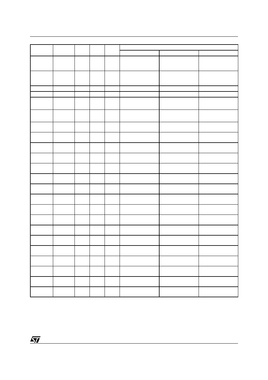
Table 1. uPSD33XX Device Selector Guide
Part No.
Main
Flash
Kbyte
2nd
Flash
Kbyte
SRAM
Kbyte
PLD
I
2
C
SPI,
Dual
UART,
IrDA
ADC,
Super-
visor
3 std
timers,
+6 prog
timer/
PWM
modules
GPIO
8032
Bus
Pins
JTAG,
ISP, &
Debug
Pkg
Op V
CC
uPSD
3312DV-
40T6
64K
16K
2K
16
macro
cells
Yes
Yes
Yes
Up to
37
No
yes
52-pin
TQFP
3.3V±10%
uPSD
3312D-
40T6
64K
16K
2K
16
macro
cells
Yes
Yes
Yes
Up to
37
No
Yes
52-pin
TQFP
3.3V &
5.0V±10%
uPSD
3333DV-
40U6
128K
32K
8K
16
macro
cells
Yes
Yes
Yes
Up to
46
Yes
Yes
80-pin
TQFP
3.3V±10%
uPSD
3333D-
40U6
128K
32K
8K
16
macro
cells
Yes
Yes
Yes
Up to
46
Yes
Yes
80-pin
TQFP
3.3V &
5.0V±10%
uPSD
3333DV-
40T6
128K
32K
8K
16
macro
cells
Yes
Yes
Yes
Up to
37
No
Yes
52-pin
TQFP
3.3V±10%
uPSD
3333D-
40T6
128K
32K
8K
16
macro
cells
Yes
Yes
Yes
Up to
37
No
Yes
52-pin
TQFP
3.3V &
5.0V±10%
uPSD
3334DV-
40T6 16
256K
32K
8K
16
macro
cells
Yes
Yes
Yes
Up to
46
Yes
Yes
80-pin
TQFP
3.3V±10%
uPSD
3334D-
40U6
256K
32K
8K
16
macro
cells
Yes
Yes
Yes
Up to
46
Yes
Yes
80-pin
TQFP
3.3V &
5.0V±10%
uPSD
3354DV-
40T6
256K
32K
32K
16
macro
cells
Yes
Yes
Yes
Up to
37
No
Yes
52-pin
TQFP
3.3V±10%
uPSD
3354D-
40T6
256K
32K
32K
16
macro
cells
Yes
Yes
Yes
Up to
37
No
Yes
52-pin
TQFP
3.3V &
5.0V±10%
uPSD
3354DV-
40T6 16
256K
32K
32K
16
macro
cells
Yes
Yes
Yes
Up to
46
Yes
Yes
80-pin
TQFP
3.3V±10%
uPSD
3354D-
40U6
256K
32K
32K
16
macro
cells
Yes
Yes
Yes
Up to
46
Yes
Yes
80-pin
TQFP
3.3V &
5.0V±10%

uPSD33XX
8/129
Figure 3. TQFP52 Connections
Note: 1. For 5V applications, V
DD
must be connected to a 5.0V source. For 3.3V applications, V
DD
must be connected to a 3.3V source.
2. These signals can be used on one of two different ports (Port 1 or Port 4) for flexibility. Default is Port1.
3. V
REF
and 3.3V V
CC
are shared in the 52-pin package only. ADC channels must use 3.3V as V
REF
for the 52-pin package.
39 P1.5/SPIRXD
(2)
/ADC5
38 P1.4/SPICLK
(2)
/ADC4
37 P1.3/TXD1(IrDA)
(2)
/ADC3
36 P1.2/RXD1(IrDA)
(2)
/ADC2
35 P1.1/T2X
(2)
/ADC1
34 P1.0/T2
(2)
/ADC0
33 V
DD
(1)
32 XTAL2
31 XTAL1
30 P3.7/I
2
CSCL
29 P3.6/I
2
CSDA
28 P3.5/C1
27 P3.4/C0
PD1/CLKIN
PC7
JTAG TDO
JTAG TDI
DEBUG
3.3V V
CC
PC4/TERR_
V
DD
(1)
GND
PC3/TSTAT
PC2/V
STBY
JTAG TCK
JTAG TMS
1
2
3
4
5
6
7
8
9
10
11
12
13
52
51
50
49
48
47
46
45
44
43
42
41
40
PB0
PB1
PB2
PB3
PB4
3.3V V
CC
/V
REF
(3)
PB5
GND
RESET_IN_
PB6
PB7
P1.7/SPISEL_
(2)
/ADC7
P1.6/SPITXD
(2)
/ADC6
14
15
16
17
18
19
20
21
22
23
24
25
26
SPISEL_
(2)
/PCACLK1/P4.7
SPITXD
(2)
/TCM5/P4.6
SPIRXD
(2)
/TCM4/P4.5
SPICLK
(2)
/TCM3/P4.4
TXD1(IrDA)
(2)
/PCACLK0/P4.3
GND
RXD1(IrDA)
(2)
/TCM2/P4.2
T2X
(2)
/TCM1/P4.1
T2
(2)
/TCM0/P4.0
RXD0/P3.0
TXD0/P3.1
EXTINT0/TG0/P3.2
EXTINT1/TG1/P3.3
AI07822

9/129
uPSD33XX
Figure 4. TQFP80 Connections
Note: NC = Not Connected
1. For 5V applications, V
DD
must be connected to a 5.0V source. For 3.3V applications, V
DD
must be connected to a 3.3V source.
2. These signals can be used on one of two different ports (Port 1 or Port 4) for flexibility. Default is Port1.
60 P1.5/SPIRXD
(2)
/ADC5
59 P1.4/SPICLK
(2)
/ADC4
58 P1.3/TXD1(IrDA)
(2)
/ADC3
57 MCU A11
56 P1.2/RXD1(IrDA)
(2)
/ADC2
55 MCU A10
54 P1.1/T2X
(2)
/ADC1
53 MCU A9
52 P1.0/T2
(2)
/ADC0
51 MCU A8
50 V
DD
(1)
49 XTAL2
48 XTAL1
47 MCU AD7
46 P3.7/I
2
CSCL
45 MCU AD6
44 P3.6/I
2
CSDA
43 MCU AD5
42 P3.5/C1
41 MCU AD4
PD2
P3.3/TG1/EXINT1
PD1
ALE
PC7
JTAG TDO
JTAG TDI
DEBUG
PC4/TERR_
3.3V V
CC
NC
V
DD
(1)
GND
PC3/TSTAT
PC2/V
STBY
JTAG TCK
NC
SPISEL_
(2)
/PCACLK1/P4.7
SPITXD
(2)
/TCM5/P4.6
JTAG TMS
1
2
3
4
5
6
7
8
9
10
11
12
13
14
15
16
17
18
19
20
80
79
78
77
76
75
74
73
72
71
70
69
68
67
66
65
64
63
62
61
PB0
P3.2/EXINT0/TG0
PB1
P3.1/TXD0
PB2
P3.0/RXD0
PB3
PB4
3.3V V
CC
PB5
V
REF
GND
RESET_IN_
PB6
PB7
RD_
P1.7/SPISEL_
(2)
/ADC7
PSEN_
WR_
P1.6/SPITXD
(2)
/ADC6
21
22
23
24
25
26
27
28
29
30
31
32
33
34
35
36
37
38
39
40
PA7
PA6
SPIRXD
(2)
/TCM4/P4.5
PA5
SPICLK
(2)
/TCM3/P4.4
PA4
TXD1(IrDA)
(2)
/PCACLK0/P4.3
PA3
GND
RXD1(IrDA)
(2)
/TCM2/P4.2
T2X
(2)
/TCM1/P4.1
PA2
T2
(2)
/TCM0/P4.0
PA1
PA0
MCU AD0
MCU AD1
MCU AD2
MCU AD3
P3.4/C0
AI07823

uPSD33XX
10/129
Table 2. Pin Descriptions
Port Pin
Signal
Name
80-Pin
No.
52-Pin
No.
(1)
In/Out
Function
Basic
Alternate 1
Alternate 2
MCUAD0
AD0
36
N/A
I/O
External Bus
Multiplexed
Address/Data bus
A0/D0
MCUAD1
AD1
37
N/A
I/O
Multiplexed
Address/Data bus
A1/D1
MCUAD2
AD2
38
N/A
I/O
Multiplexed
Address/Data bus
A2/D2
MCUAD3
AD3
39
N/A
I/O
Multiplexed
Address/Data bus
A3/D3
MCUAD4
AD4
41
N/A
I/O
Multiplexed
Address/Data bus
A4/D4
MCUAD5
AD5
43
N/A
I/O
Multiplexed
Address/Data bus
A5/D5
MCUAD6
AD6
45
N/A
I/O
Multiplexed
Address/Data bus
A6/D6
MCUAD7
AD7
47
N/A
I/O
Multiplexed
Address/Data bus
A7/D7
MCUA8
A8
51
N/A
O
External Bus, Addr
A8
MCUA9
A9
53
N/A
O
External Bus, Addr
A9
MCUA10
A10
55
N/A
O
External Bus, Addr
A10
MCUA11
A11
57
N/A
O
External Bus, Addr
A11
P1.0
T2 ADC0
52
34
I/O
General I/O port pin
Timer 2 Count input
(T2)
ADC Channel 0
input (ADC0)
P1.1
T2EX
ADC1
54
35
I/O
General I/O port pin
Timer 2 Trigger input
(T2X)
ADC Channel 1
input (ADC1)
P1.2
RxD1
ADC2
56
36
I/O
General I/O port pin
UART1 or IrDA
Receive (RxD1)
ADC Channel 2
input (ADC2)
P1.3
TXD1
ADC3
58
37
I/O
General I/O port pin
UART or IrDA
Transmit (TxD1)
ADC Channel 3
input (ADC3)
P1.4
SPICLK
ADC4
59
38
I/O
General I/O port pin
SPI Clock Out
(SPICLK)
ADC Channel 4
input (ADC4)
P1.5
SPIRxD
ADC6
60
39
I/O
General I/O port pin
SPI Receive
(SPIRxD)
ADC Channel 5
input (ADC5)
P1.6
SPITXD
ADC6
61
40
I/O
General I/O port pin
SPI Transmit
(SPITxD)
ADC Channel 6
input (ADC6)
P1.7
SPISEL
ADC7
64
41
I/O
General I/O port pin
SPI Slave Select
(SPISEL)
ADC Channel 7
input (ADC7)
P3.0
RxD0
75
23
I/O
General I/O port pin
UART0 Receive
(RxD0)
P3.1
TXD0
77
24
I/O
General I/O port pin
UART0 Transmit
(TxD0)
11/129
uPSD33XX
P3.2
EXINT0
TGO
79
25
I/O
General I/O port pin
Interrupt 0 input
(EXTINT0)/Timer 0
gate control (TG0)
P3.3
INT1
2
26
I/O
General I/O port pin
Interrupt 1 input
(EXTINT1)/Timer 1
gate control (TG1)
P3.4
C0
40
27
I/O
General I/O port pin
Counter 0 input (C0)
P3.5
C1
42
28
I/O
General I/O port pin
Counter 1 input (C1)
P3.6
I
2
CSDA
44
29
I/O
General I/O port pin
I
2
C Bus serial data
(I
2
CSDA)
P3.7
I
2
CSCL
46
30
I/O
General I/O port pin
I
2
C Bus clock
(I
2
CSCL)
P4.0
T2 TCM0
33
22
I/O
General I/O port pin
Program Counter
Array0 PCA0-TCM0
Timer 2 Count input
(T2)
P4.1
T2X
TCM1
31
21
I/O
General I/O port pin
PCA0-TCM1
Timer 2 Trigger input
(T2X)
P4.2
RXD1
TCM2
30
20
I/O
General I/O port pin
PCA0-TCM2
UART1 or IrDA
Receive (RxD1)
P4.3
TXD1
PCACLK0
27
18
I/O
General I/O port pin
PCACLK0
UART1 or IrDA
Transmit (TxD1)
P4.4
SPICLK
TCM3
25
17
I/O
General I/O port pin
Program Counter
Array1 PCA1-TCM3
SPI Clock Out
(SPICLK)
P4.5
SPIRXD
TCM4
23
16
I/O
General I/O port pin
PCA1-TCM4
SPI Receive
(SPIRxD)
P4.6
SPITXD
19
15
I/O
General I/O port pin
PCA1-TCM5
SPI Transmit
(SPITxD)
P4.7
SPISEL
PCACLK1
18
14
I/O
General I/O port pin
PCACLK1
SPI Slave Select
(SPISEL)
V
REF
70
N/A
I
Reference Voltage
input for ADC
RD_
65
N/A
O
READ Signal,
external bus
WR_
62
N/A
O
WRITE Signal,
external bus
PSEN_
63
N/A
O
PSEN Signal,
external bus
ALE
4
N/A
O
Address Latch
signal, external bus
RESET_
IN_
68
44
I
Active low reset
input
XTAL1
48
31
I
Oscillator input pin
for system clock
XTAL2
49
32
O
Oscillator output pin
for system clock
DEBUG
8
5
I/O
I/O to the MCU
Debug Unit
Port Pin
Signal
Name
80-Pin
No.
52-Pin
No.
(1)
In/Out
Function
Basic
Alternate 1
Alternate 2

uPSD33XX
12/129
Note: 1. N/A = Signal Not Available on 52-pin package.
PA0
35
N/A
I/O
General I/O port pin
All Port A pins
support:
1. PLD Macro-cell
outputs, or
2. PLD inputs, or
3. Latched Address
Out (A0-A7), or
4. Peripheral I/O
Mode
PA1
34
N/A
I/O
General I/O port pin
PA2
32
N/A
I/O
General I/O port pin
PA3
28
N/A
I/O
General I/O port pin
PA4
26
N/A
I/O
General I/O port pin
PA5
24
N/A
I/O
General I/O port pin
PA6
22
N/A
I/O
General I/O port pin
PA7
21
N/A
I/O
General I/O port pin
PB0
80
52
I/O
General I/O port pin
All Port B pins
support:
1. PLD Macro-cell
outputs, or
2. PLD inputs, or
3. Latched Address
Out (A0-A7)
PB1
78
51
I/O
General I/O port pin
PB2
76
50
I/O
General I/O port pin
PB3
74
49
I/O
General I/O port pin
PB4
73
48
I/O
General I/O port pin
PB5
71
46
I/O
General I/O port pin
PB6
67
43
I/O
General I/O port pin
PB7
66
42
I/O
General I/O port pin
JTAGTMS
TMS
20
13
I
JTAG pin (TMS)
JTAGTCK
TCK
16
12
I
JTAG pin (TCK)
PC2
V
STBY
15
11
I/O
General I/O port pin
SRAM Standby
voltage input
(V
STBY
)
PLD Macrocell
output, or PLD input
PC3
TSTAT
14
10
I/O
General I/O port pin
Optional JTAG
Status (TSTAT)
PLD, Macrocell
output, or PLD input
PC4
TERR_
9
7
I/O
General I/O port pin
Optional JTAG
Status (TERR_)
PLD, Macrocell
output, or PLD input
JTAGTDI
TDI
7
4
I
JTAG pin (TDI)
JTAGTDO
TDO
6
3
O
JTAG pin (TDO)
PC7
5
2
I/O
General I/O port pin
PLD, Macrocell
output, or PLD input
PD1
CLKIN
3
1
I/O
General I/O port pin
1. PLD I/O
2. Clock input to
PLD and APD
PD2
CSI
1
N/A
I/O
General I/O port pin
1. PLD I/O
2. Chip select ot
PSD Module
3.3V-V
CC
10
6
V
CC
- MCU Module
3.3V-V
CC
72
47
V
CC
- MCU Module
V
DD
3.3V or 5V
12
8
V
DD
- PSD Module
V
DD
- 3.3V for 3V
V
DD
- 5V for 5V
V
DD
3.3V or 5V
50
33
V
DD
- PSD Module
V
DD
- 3.3V for 3V
V
DD
- 5V for 5V
GND
13
9
GND
29
19
GND
69
45
NC
11
N/A
NC
17
N/A
Port Pin
Signal
Name
80-Pin
No.
52-Pin
No.
(1)
In/Out
Function
Basic
Alternate 1
Alternate 2

13/129
uPSD33XX
uPSD33XX HARDWARE DESCRIPTION
The uPSD33XX has a modular architecture built
from a stacked die process. There are two die, one
is designated "MCU Module" in this document,
and the other is designated "PSD Module" (see
Figure 5, page 14). In all cases, the MCU Module
die operates at 3.3V with 5V tolerant I/O. The PSD
Module is either a 3.3V die or a 5V die, depending
on the uPSD33XX device as described below.
The MCU Module consists of a fast 8032 core, that
operates with 4 clocks per instruction cycle, and
has many peripheral and system supervisor func-
tions. The PSD Module provides the 8032 with
multiple memories (two Flash and one SRAM) for
program and data, programmable logic for ad-
dress decoding and for general-purpose logic, and
additional I/O. The MCU Module communicates
with the PSD Module through internal address and
data busses (A8 ≠ A15, AD0 ≠ AD7) and control
signals (RD_, WR_, PSEN_, ALE, RESET_).
There are slightly different I/O characteristics for
each module. I/Os for the MCU module are desig-
nated as Ports 1, 3, and 4. I/Os for the PSD Mod-
ule are designated as Ports A, B, C, and D.
For all 5V uPSD33XX devices, a 3.3V MCU Mod-
ule is stacked with a 5V PSD Module. In this case,
a 5V uPSD33XX device must be supplied with
3.3VCC for the MCU Module and 5.0VDD for the
PSD Module. Ports 1, 3, and 4 of the MCU Module
are 3.3V ports with tolerance to 5V devices (they
can be directly driven by external 5V devices and
they can directly drive external 5V devices while
producing a V
OH
of 2.4V min and V
CC
max). Ports
A, B, C, and D of the PSD Module are true 5V
ports.
For all 3.3V uPSD33XXV devices, a 3.3V MCU
Module is stacked with a 3.3V PSD Module. In this
case, a 3.3V uPSD33XX device needs to be sup-
plied with a single 3.3V voltage source at both V
CC
and V
DD
. I/O pins on Ports 1, 3, and 4 are 5V tol-
erant and can be connected to external 5V periph-
erals devices if desired. Ports A, B, C, and D of the
PSD Module are 3.3V ports, which are not tolerant
to external 5V devices.
Refer to Table 3 for port type and voltage source
requirements.
80-pin uPSD33XX devices provide access to 8032
address, data, and control signals on external pins
to connect external peripheral and memory devic-
es. 52-pin uPSD33XX devices do not provide ac-
cess to the 8032 system bus.
All non-volatile memory and configuration portions
of the uPSD33XX device are programmed through
the JTAG interface and no special programming
voltage is needed. This same JTAG port is also
used for debugging and emulation of the 8032
core at runtime providing breakpoint, single-step,
display, and trace features. A non-volatile security
bit may be programmed to block all access via
JTAG interface for security. The security bit is de-
feated only by erasing the entire device, leaving
the device blank and ready to use again.
Table 3. Port Type and Voltage Source Combinations
Device Type
V
CC
for MCU
Module
V
DD
for PSD
Module
Ports 1, 3, and 4 on MCU
Module
Ports A, B, C, and D on
PSD Module
5V:
uPSD33XX
3.3V
5.0V
3.3V but 5V tolerant
5V
3.3V:
uPSD33XXV
3.3V
3.3V
3.3V but 5V tolerant
3.3V. NOT 5V tolerant

uPSD33XX
14/129
Figure 5. uPSD33XX Functional Modules
10-bit
ADC
Dedicated Memory
Interface
Prefetch, Jump Cache
Enhanced MCU Interface
Decode PLD
PSD Page Register
SRAM
CPLD - 16 MACROCELLS
JTAG ISP
Reset Logic
WDT
Internal
Reset
Port 1
Port 3
Dual
UARTs
Interrupt
3 Timer /
Counters
256 Byte SRAM
Turbo 8032 Core
PSD Internal Bus
8032 Internal Bus
PSD
Reset
LVD
I
2
C
Unit
Port D
GPIO
Port C
JTAG and
GPIO
Secondary
Flash
Reset Input
uPSD33XX
JTAG
DEBUG
8-Bit Die-to-Die Bus
Main Flash
PCA
PWM
Counters
Reset
Pin
Ext.
Bus
SPI
V
CC
Pins
3.3V
V
DD
Pins
3.3V or 5V
MCU Module
PSD Module
Port 3 - UART0,
Intr, Timers
Port 1 - Timer, ADC, SPI
Port 4 - PCA,
PWM, UART1
Port 3
I
2
C
XTAL
Clock Unit
Port A,B,C PLD
I/O and GPIO
AI07842

15/129
uPSD33XX
MEMORY ORGANIZATION
The 8032 MCU core views memory on the MCU
module as "internal" memory and it views memory
on the PSD module as "external" memory, see
Figure 6.
Internal memory on the MCU Module consists of
DATA, IDATA, and SFRs. These standard 8032
memories reside in 384 bytes of SRAM located at
a fixed address space starting at address 0x0000.
External memory on the PSD Module consists of
four types: main Flash (64K, 128K, or 256K bytes),
a smaller secondary Flash (16K, or 32K), SRAM
(2K, 8K, or 32K bytes), and a block of PSD Module
control registers called CSIOP (256 bytes). These
external memories reside at programmable ad-
dress ranges, specified using the software tool
PSDsoft Express. See the PSD Module section of
this document for more details on these memories.
External memory is accessed by the 8032 in two
separate 64K byte address spaces. One address
space is for program memory and the other ad-
dress space is for data memory. Program memory
is accessed using the 8032 signal, PSEN_. Data
memory is accessed using the 8032 signals, RD_
and WR_. If the 8032 needs to access more than
64K bytes of external program or data memory, it
must use paging (or banking) techniques provided
by the Page Register in the PSD Module.
Note: When referencing program and data mem-
ory spaces, it has nothing to do with 8032 internal
SRAM areas of DATA, IDATA, and SFR on the
MCU Module. Program and data memory spaces
only relate to the external memories on the PSD
Module.
External memory on the PSD Module can overlap
the internal SRAM memory on the MCU Module in
the same physical address range (starting at
0x0000) without interference because the 8032
core does not assert the RD_ or WR_ signals
when accessing internal SRAM.
Figure 6. uPSD33XX Memories
∑ External memories may be placed at virtually
any address using software tool PSDsoft Express.
∑ The SRAM and Flash memories may be placed
in 8032 Program Space or Data Space using
PSDsoft Express.
∑ Any memory in 8032 Data Space is XDATA.
64KB,
128KB,
or
256KB
16KB
or
32KB
Main
Flash
Internal SRAM on
MCU Module
External Memory on
PSD Module
IDATA
SFR
DATA
Secondary
Flash
2KB,
8KB,
or
32KB
SRAM
256 Bytes
CSIOP
384 Bytes SRAM
Direct or Indirect Addressing
FF
80
7F
128 Bytes
128 Bytes
128 Bytes
0
Indirect
Addressing
Fixed
Addresses
Direct
Addressing
AI07843

uPSD33XX
16/129
Internal Memory (MCU Module, Standard 8032
Memory: DATA, IDATA, SFR)
DATA Memory. The first 128 bytes of internal
SRAM ranging from address 0x0000 to 0x007F
are called DATA, which can be accessed using
8032 direct or indirect addressing schemes and
are typically used to store variables and stack.
Four register banks, each 8 registers wide (R0 ≠
R7), occupy addresses 0x0000 to 0x001F. Only
one of these four banks may be enabled at a time.
The next 16 locations at 0x0020 to 0x002F contain
128 directly addressable bit locations that can be
used as software flags. SRAM locations 0x0030
and above may be used for variables and stack.
IDATA Memory. The next 128 bytes of internal
SRAM are named IDATA and range from address
0x0080 to 0x00FF. IDATA can be accessed only
through 8032 indirect addressing and is typically
used to hold the MCU stack as well as data vari-
ables. The stack can reside in both DATA and
IDATA memories and reach a size limited only by
the available space in the combined 256 bytes of
these two memories (since stack accesses are al-
ways done using indirect addressing, the bound-
ary between DATA and IDATA does not exist with
regard to the stack).
SFR Memory. Special Function Registers (Table
4, page 21) occupy a separate physical memory,
but they logically overlap the same 128 bytes as
IDATA, ranging from address 0x0080 to 0x00FF.
SFRs are accessed only using direct addressing.
There 92 active registers used for many functions:
changing the operating mode of the 8032 MCU
core, controlling 8032 peripherals, controlling I/O,
and managing interrupt functions. The remaining
unused SFRs are reserved and should not be ac-
cessed.
16 of the SFRs are both byte- and bit-addressable.
Bit-addressable SFRs are those whose address
ends in "0" or "8" hex as indicated by "*" in Table 4,
page 21.
External Memory (PSD Module: Program
memory, Data memory)
The PSD Module has four memories: main Flash,
secondary Flash, SRAM, and CSIOP. See the
PSD MODULE section for more detailed informa-
tion on these memories.
Memory mapping in the PSD Module is imple-
mented with the Decode PLD (DPLD) and option-
ally the Page Register. The user specifies decode
equations for individual segments of each of the
memories using the software tool PSDsoft Ex-
press. This is a very easy point-and-click process
allowing total flexibility in mapping memories. Ad-
ditionally, each of the memories may be placed in
various combinations of 8032 program address
space or 8032 data address space by using the
software tool PSDsoft Express.
Program Memory. External program memory is
addressed by the 8032 using its 16-bit Program
Counter (PC) and is accessed with the 8032 sig-
nal, PSEN_. Program memory can be present at
any address in program space between 0x0000
and 0xFFFF.
After a power-up or reset, the 8032 begins execu-
tion from location 0x0000 where the reset vector is
stored, causing a jump to an initialization routine in
firmware. At address 0x0003, just following the re-
set vector are the interrupt service locations. Each
interrupt is assigned a fixed interrupt service loca-
tion in program memory. An interrupt causes the
8032 to jump to that service location, where it com-
mences execution of the service routine. External
Interrupt 0 (EXINT0), for example, is assigned to
service location 0x0003. If EXINT0 is going to be
used, its service routine must begin at location
0x0003. Interrupt service locations are spaced at
8-byte intervals: 0x0003 for EXINT0, 0x000B for
Timer 0, 0x0013 for EXINT1, and so forth. If an in-
terrupt service routine is short enough, it can re-
side entirely within the 8-byte interval. Longer
service routines can use a jump instruction to
somewhere else in program memory.
Data Memory. External data is referred to as
XDATA and is addressed by the 8032 using Indi-
rect Addressing via its 16-bit Data Pointer Register
(DPTR) and is accessed by the 8032 signals, RD_
and WR_. XDATA can be present at any address
in data space between 0x0000 and 0xFFFF.
Note: the uPSD33XX has dual data pointers
(source and destination) making XDATA transfers
much more efficient.
Memory Placement. PSD Module architecture
allows the placement of its external memories into
different combinations of program memory and
data memory spaces. This means the main Flash,
the secondary Flash, and the SRAM can be
viewed by the 8032 MCU in various combinations
of program memory or data memory as defined by
PSDsoft Express.
As an example of this flexibility, for applications
that require a great deal of Flash memory in data
space (large lookup tables or extended data re-
cording), the larger main Flash memory can be
placed in data space and the smaller secondary
Flash memory can be placed in program space.
The opposite can be realized for a different appli-
cation if more Flash memory is needed for code
and less Flash memory for data.

17/129
uPSD33XX
By default, the SRAM and CSIOP memories on
the PSD Module must always reside in data mem-
ory space and they are treated by the 8032 as
XDATA. However, the SRAM may optionally re-
side in program space in addition to data space if
it is desired to execute code from SRAM. The main
Flash and secondary Flash memories may reside
in program space, data space, or both.
These memory placement choices specified by
PSDsoft Express are programmed into non-vola-
tile sections of the uPSD33XX, and are active at
power-up and after reset. It is possible to override
these initial settings during runtime for In-Applica-
tion Programming (IAP).
Standard 8032 MCU architecture cannot write to
its own program memory space to prevent acci-
dental corruption of firmware. However, this be-
comes an obstacle in typical 8032 systems when
a remote update to firmware in Flash memory is
required using IAP. The PSD module provides a
solution for remote updates by allowing 8032 firm-
ware to temporarily "reclassify" Flash memory to
reside in data space during a remote update, then
returning Flash memory back to program space
when finished. See the VM Register (Table 84,
page 81) in the PSD Module section of this docu-
ment for more details.
8032 MCU CORE PERFORMANCE ENHANCEMENTS
Before describing performance features of the
uPSD33XX, let us first look at standard 8032 ar-
chitecture. The clock source for the 8032 MCU
creates a basic unit of timing called a machine-cy-
cle, which is a period of 12 clocks for standard
8032 MCUs. The instruction set for traditional
8032 MCUs consists of 1, 2, and 3 byte instruc-
tions that execute in different combinations of 1, 2,
or 4 machine-cycles. For example, there are one-
byte instructions that execute in one machine-cy-
cle (12 clocks), one-byte instructions that execute
in four machine-cycles (48 clocks), two-byte, two-
cycle instructions (24 clocks), and so on. In addi-
tion, standard 8032 architecture will fetch two
bytes from program memory on almost every ma-
chine-cycle, regardless if it needs them or not
(dummy fetch). This means for one-byte, one-cy-
cle instructions, the second byte is ignored. These
one-byte, one-cycle instructions account for half of
the 8032's instructions (126 out of 255 opcodes).
You can see that there are inefficiencies due to
wasted bus cycles and idle bus times that can be
eliminated.
The uPSD33XX 8032 MCU core offers increased
performance in a number of ways, while keeping
the exact same instruction set as the standard
8032 (all opcodes, the number of bytes per in-
struction, and the native number a machine-cycles
per instruction are identical to the original 8032).
The first way performance is boosted is by reduc-
ing the machine-cycle period to just 4 MCU clocks
as compared to 12 MCU clocks in a standard
8032. This shortened machine-cycle improves the
instruction rate for one-byte, one-cycle instruc-
tions by a factor of three (Figure 7, page 18) com-
pared to standard 8051 architectures, and
significantly improves performance of multiple-cy-
cle instruction types.
The example in Figure 7, page 18 shows a contin-
uous execution stream of one-byte, one-cycle in-
structions. The 5V uPSD33XX will yield 10 MIPS
peak performance in this case while operating at
40MHz clock rate. In a typical application however,
the effective performance will be lower since pro-
grams do not use only one-cycle instructions, but
special techniques are implemented in the
uPSD33XX to keep the effective MIPS rate as
close as possible to the peak MIPS rate at all
times. This is accomplished with an instruction
Pre-Fetch Queue (PFQ) and a Branch Cache (BC)
as shown in Figure 8, page 18.

uPSD33XX
18/129
Figure 7. Comparison of uPSD33XX with Standard 8032 Performance
Figure 8. Instruction Pre-Fetch Queue and Branch Cache
MCU Clock
Standard 8032
Fetch Byte for Instruction A
Execute Instruction A
and Fetch a Second Dummy Byte
Turbo uPSD33XX
Execute Instruction and
Pre-Fetch Next Instruction
4 clocks (one machine cycle)
12 clocks (one machine cycle)
1-byte, 1-Cycle Instructions
Dummy Byte is Ignored (wasted bus access)
Execute Instruction and
Pre-Fetch Next Instruction
Execute Instruction and
Pre-Fetch Next Instruction
Instruction A
Instruction B
Instruction C
Instruction A
Turbo uPSD33XX executes instructions A, B, and C in the same
amount of time that a standard 8032 executes only instruction A.
one machine cycle
one machine cycle
AI08808
Branch 4
Code
Branch 4
Code
Branch 4
Code
Branch 4
Code
Branch 4
Code
Branch 4
Code
Previous
Branch 4
8032
MCU
Program
Memory on
PSD Module
Instruction Pre-Fetch Queue (PFQ)
6 Bytes of Instruction
Instruction
Byte
Wait
Stall
8
Instruction
Byte
8
Current
Branch
Address
Compare
Branch
Cache
(BC)
16
AI08809
Address
16
Address
Load on Branch Address Match
Branch 3
Code
Branch 3
Code
Branch 3
Code
Branch 3
Code
Branch 3
Code
Branch 3
Code
Previous
Branch 3
Branch 2
Code
Branch 2
Code
Branch 2
Code
Branch 2
Code
Branch 2
Code
Branch 2
Code
Previous
Branch 2
Branch 1
Code
Branch 1
Code
Branch 1
Code
Branch 1
Code
Branch 1
Code
Branch 1
Code
Previous
Branch 1
Address

19/129
uPSD33XX
Pre-Fetch Queue (PFQ) and Branch Cache
(BC)
The PFQ is always working to minimize the idle
bus time inherent to 8032 MCU architecture, to
eliminate wasted memory fetches, and to maxi-
mize memory bandwidth to the MCU. The PFQ
does this by running asynchronously in relation to
the MCU, looking ahead to pre-fetch code from
program memory during any idle bus periods. Only
necessary bytes will be fetched (no dummy fetch-
es like standard 8032). The PFQ will queue up to
six code bytes in advance of execution, which sig-
nificantly optimizes sequential program perfor-
mance. However, when program execution
becomes non-sequential (program branch), a typ-
ical pre-fetch queue will empty itself and reload
new code, causing the MCU to stall. The Turbo
uPSD33XX diminishes this problem by using a
Branch Cache with the PFQ. The BC is a four-way,
fully associative cache, meaning that when a pro-
gram branch occurs, it's branch destination ad-
dress is compared simultaneously with four recent
previous branch destinations stored in the BC.
Each of the four cache entries contain up to six
bytes of code related to a branch. If there is a hit
(a match), then all six code bytes of the matching
program branch are transferred immediately and
simultaneously from the BC to the PFQ, and exe-
cution on that branch continues with minimal de-
lay. This greatly reduces the chance that the MCU
will stall from an empty PFQ, and improves perfor-
mance in embedded control systems where it is
quite common to branch and loop in relatively
small code localities.
By default, the PFQ and BC are enabled after
power-up or reset. The 8032 can disable the PFQ
and BC at runtime if desired by writing to a specific
SFR (BUSCON).
The memory in the PSD module operates with
variable wait states depending on the value spec-
ified in the SFR named BUSCON. For example, a
5V uPSD33XX device operating at a 40MHz crys-
tal frequency requires four memory wait states
(equal to four MCU clocks). In this example, once
the PFQ has one or more bytes of code, the wait
states become transparent and a full 10 MIPS is
achieved when the program stream consists of se-
quential one-byte, one machine-cycle instructions
as shown in Figure 7, page 18 (transparent be-
cause a machine-cycle is four MCU clocks which
equals the memory pre-fetch wait time that is also
four MCU clocks). But it is also important to under-
stand PFQ operation on multi-cycle instructions.
PFQ Example, Multi-cycle Instructions
Let us look at a string of two-byte, two-cycle in-
structions in Figure 9, page 20. There are three in-
structions executed sequentially in this example,
instructions A, B,and C. Each of the time divisions
in the figure is one machine-cycle of four clocks,
and there are six phases to reference in this dis-
cussion. Each instruction is pre-fetched into the
PFQ in advance of execution by the MCU. Prior to
Phase 1, the PFQ has pre-fetched the two instruc-
tion bytes (A1 and A2) of instruction A. During
Phase one, both bytes are loaded into the MCU
execution unit. Also in Phase 1, the PFQ is pre-
fetching the first byte (B1) of instruction B from
program memory. In Phase 2, the MCU is pro-
cessing Instruction A internally while the PFQ is
pre-fetching the second byte (B2) of Instruction B.
In Phase 3, both bytes of instruction B are loaded
into the MCU execution unit and the PFQ begins
to pre-fetch bytes for the third instruction C. In
Phase 4 Instruction B is processed and the pre-
fetching continues, eliminating idle bus cycles and
feeding a continuous flow of operands and op-
codes to the MCU execution unit.
The uPSD33XX MCU instructions are an exact 1/
3 scale of all standard 8032 instructions with re-
gard to number of cycles per instruction. Figure
10, page 20 shows the equivalent instruction se-
quence from the example above on a standard
8032 for comparison.
Aggregate Performance
The stream of two-byte, two-cycle instructions in
Figure 9, page 20, running on a 40MHz, 5V,
uPSD33XX will yield 5 MIPs. And we saw the
stream of one-byte, one-cycle instructions in Fig-
ure 7, page 18 on the same MCU yield 10 MIPs.
Your effective performance will depend on a num-
ber of things: your MCU clock frequency; the mix-
ture of instructions types (bytes and cycles) in your
application; the amount of time an empty PFQ
stalls the MCU (mix of instruction types and miss-
es on Branch Cache); and the operating voltage.
A 5V uPSD33XX device operates with four mem-
ory wait states, but a 3.3V devices operates with
five memory wait states yielding 8 MIPS peak
compared to 10 MIPs peak for 5V devices. The
same number of wait states will apply to both pro-
gram fetches and to data READ/WRITEs unless
otherwise specified in the SFR named BUSCON.
In general, a 3X aggregate performance increase
is expected over any standard 8032 application
running at the same clock frequency.

uPSD33XX
20/129
Figure 9. PFQ Operation on Multi-cycle Instructions
Figure 10. uPSD33XX Multi-cycle Instructions Compared to Standard 8032
Inst A, Byte 1
Three 2-byte, 2-cycle Instructions on uPSD33XX
PFQ
MCU
Execution
Inst A, Byte 2 Inst B, Byte 1 Inst B, Byte 2 Inst C, Byte 1 Inst C, Byte 2
Previous Instruction
A1
A2
Process A
B1
B2
Process B
C1
C2
AI08810
Process C
Continue to Pre-Fetch
Next Inst
4-clock
Macine Cycle
Instruction A
Instruction B
Instruction C
Pre-Fetch Inst A
Pre-Fetch Inst B
Pre-Fetch Inst C
Phase 1
Phase 2
Phase 3
Phase 4
Phase 6
Phase 5
A1
A2
Inst A
B1
B2
Inst B
C1 C2
Inst C
Three 2-byte, 2-cycle Instructions, uPSD33XX vs. Standard 8032
uPSD33XX
Std 8032
72 Clocks (12 clocks per cycle)
24 Clocks Total (4 clocks per cycle)
Byte 1
Byte 2
Process Inst A
Byte 1
Byte 2
Process Inst B
Byte 1
Byte 2
Process Inst C
AI08811
1 Cycle
1 Cycle

21/129
uPSD33XX
MCU MODULE DISCRIPTION
This section provides a detail description of the
MCU Module system functions and Peripherals,
including:
≠ Special Function Registers
≠ Debug Unit
≠ Interrupts
≠ Power Saving Modes
≠ Oscillator and MCU Clock Generation
≠ I/O Ports
≠ MCU Bus Interface
≠ Supervisory Function (LVD and Watchdog)
≠ Timers/Counter
≠ UART
≠ IrDA Interface
≠ I
2
C Bus
≠ SPI Bus
≠ ADC
≠ Programmable Counter Array (PCA)
Special Function Registers (SFRs)
A map of the on-chip memory area called the Spe-
cial Function Register (SFR) space is shown in Ta-
ble 4. The SFRs can only be addressed directly in
the address range from 80h to FFh. Sixteen ad-
dress in the SFR space are both: byte- and bit-ad-
dressable. The bit-addressable SFRs are those
whose address ends in 0h and 8h (as indicated by
* in the table).
Note: In the SFRs not all of the addresses are oc-
cupied. Unoccupied addresses are not implement-
ed on the chip and are reserved.
Table 4. SFR Memory Map
F8
CCON0
CCON2
CCON3
FF
F0
*B
F7
E8
EF
E0
*ACC
UDT1
UDT0
E7
D8
*SCON1
SBUF1
S1SETUP
S1CON
S1STA
S1DAT
S1ADR
DF
D0
*PSW
SPICLKD
SPISTAT
SPITDR
SPIRDR
SPICON0
SPICON1
D7
C8
*T2CON
RCAP2L
RCAP2H
TL2
TH2
IRDACON
DSTAT
CF
C0
*P4
CAPCOM
L3
CAPCOM
H3
CAPCOM
L4
CAPCOM
H4
CAPCOM
L5
CAPCOM
H5
PWMF1
C7
B8
*IP
PCACL1
PCACH1
PCACON1
TCM
MODE3
TCM
MODE4
TCM
MODE5
BF
B0
*P3
CAPCOM
H1
CAPCOM
L2
CAPCOM
H2
PWMF0
IPA
B7
A8
*IE
TCM
MODE0
TCM
MODE1
TCM
MODE2
CAPCOM
L0
CAPCOM
H0
WDKEY
CAPCOM
L1
AF
A0
*P2
PCACL0
PCACH0
PCACON0
PCASTA
WDRST
IEA
A7
98
*SCON0
SBUF0
BUSCON
DIR
DVR
9F
90
*P1
P3SFS
P4SFS0
P4SFS1
ADC0S
ADAT0
ADAT1
ACON
97
88
*TCON
TMOD
TL0
TL1
TH0
TH1
P1SFS0
P1SFS1
8F
80
*P0
SP
DPL
DPH
DPTC
PDTM
PCON
87

uPSD33XX
22/129
Dual Data Pointers
Data read access to the program memory and
READ/WRITE access to the XRAM are executed
using the data pointer DPTR as a 16-bit address
register for indirect addressing mode. The DPTR
consists of a high byte (DPH, 83H) and a low byte
(DPL, 82H). Its intended function is to hold a 16-bit
address. It may be manipulated as a 16-bit register
or as two independent 8-bit registers.
The uPSD33XX has two data pointers (DPTR0
and DPTR1), one of which is selected by Bit
DPSEL0 in the Data Pointer Control Register
DPTC. After reset, these registers are set to "00H."
Only one DPTR is active at any time, and the se-
lected PDTR resides in SFR address 83H and
82H. The DPTR which is not selected remains in
the background and is not accessible by the CPU.
Data Pointer Control Register, DPTC (85H)
The control register allows the DPTR to be select-
ed manually, or automatically switching between
the two data pointers. Bit DPSEL0 selects one of
two pointers. The automatic switching between
DPTR0 and DPTR1 is controlled by Bit AT (Auto
Toggle). When Bit AT is set, Bit DPSEL0 is toggled
automatically every time after the DPTR is access-
ed. Detailed description for register DPTC is
shown in Table 5 and Table 6.
The data pointer currently selected by the PSEL0
Bit can be modified, whereas the other data point-
ers are kept in the background and remain un-
changed.
Table 5. Data Pointer Control Register, DPTC, Bit Definition (85H, Reset Value 00H)
Table 6. Data Pointer Control Register Details
Note: Standard increment instruction on Register DPTC can be used to toggle Bit DPSEL0.
Bit 7
Bit 6
Bit 5
Bit 4
Bit 3
Bit 2
Bit 1
Bit 0
≠
AT
≠
≠
≠
≠
≠
DPSEL0
BIT
SYMBOL
RW
Definition
7
≠
Reserved
6
AT
RW
0 = Manual Select Data Pointer
1 = Auto Toggle between DPTR0 and DPTR1
5-1
≠
Reserved
0
DPSE0
RW
0 = DPTR0 Selected
1 = DPTR1 Selected

23/129
uPSD33XX
Data Pointer Mode Register, DPTM (86H)
The uPSD33XX provides automatic increment or
decrement of content of the working DPTR
through the DPTM register. The content of the
working DPTR is modified at the access time. De-
tailed description for DPTM is shown in Table 7
and Table 8.
The automatic decrement or increment function in
the DPTM Register is effective only for the MOVX
instruction.
Table 7. Data Pointer Mode Register, DPTM Bit Definition (86H, Reset Value 00H)
Table 8. Data Pointer Mode Register Details
Debug Unit
The MCU Module has a Debug Unit which sup-
ports debugging functions that are required in new
PC board development. The JTAG port in the
uPSD33XX is responsible for communications be-
tween the host development system and the De-
bug Unit. The basic debugging functions
supported include:
≠ Halt or Start CPU execution
≠ Reset the CPU
≠ Single Step
≠ Four breakpoints, breaks on address/data
≠ Debug Interrupt to CPU at breakpoint
≠ Program tracing
≠ READ/WRITE to SFR, PC and Memory
The Debug pin can be configured in the host sys-
tem to generate an output pulse for external trig-
gering when a break condition is met. It can also
be configured as an event input to the breakpoint
logic in the Debug Unit. If not used, this pin should
be pulled high.
Bit 7
Bit 6
Bit 5
Bit 4
Bit 3
Bit 2
Bit 1
Bit 0
≠
≠
≠
≠
MD11
MD10
MD01
MD00
BIT
SYMBOL
RW
Definition
7-4
≠
Reserved
3-2
MD[11:10]
RW
DPTR1 Mode Bits
00: DPTR1 No Change
01: Reserved
10: Auto Increment
11: Auto Decrement
1-0
MD[01:00]
RW
DPTR0 Mode Bits
00: DPTR0 No Change
01: Reserved
10: Auto Increment
11: Auto Decrement

uPSD33XX
24/129
INTERRUPT SYSTEM
There are interrupt requests from 10 sources as
follows:
s
Debug Interrupt
s
INT0 External Interrupt
s
UART0 and UART1 Interrupt
s
Timer 0 Interrupt
s
I
2
C Interrupt
s
INT1 External Interrupt
s
ADC Interrupt
s
Timer 1 Interrupt
s
SPI Interrupt
s
Timer 2 Interrupt
s
PCA Interrupt
External Int0
≠ The INT0 can be either level-active or
transition-active depending on Bit IT0 in
register TCON. The flag that actually
generates this interrupt is Bit IE0 in TCON.
≠ When an external interrupt is generated, the
corresponding request flag is cleared by the
hardware when the service routine is
vectored to only if the interrupt was transition
activated.
≠ If the interrupt was level activated then the
interrupt request flag remains set until the
requested interrupt is actually generated.
Then it has to deactivate the request before
the interrupt service routine is completed, or
else another interrupt will be generated.
Timer 0 and 1 Inputs
≠ Timer 0 and Timer 1 Interrupts are generated
by TF0 and TF1 which are set by an overflow
of their respective Timer/Counter registers
(except for Timer 0 in Mode 3).
≠ These flags are cleared by the internal
hardware when the interrupt is serviced.
Timer 2 Interrupt
≠ Timer 2 Interrupt is generated by TF2 which
is set by an overflow of Timer 2. This flag has
to be cleared by the software - not by
hardware.
≠ It is also generated by the T2EX signal (Timer
2 External Interrupt P1.1) which is controlled
by EXEN2 and EXF2 Bits in the T2CON
register.
I
2
C Interrupt
≠ The interrupt of the I
2
C is generated by Bit
INTR in the register S1STA.
≠ This flag is cleared by hardware.
External Int1
≠ The INT1 can be either level-active or
transition-active, depending on Bit IT1 in
register TCON.
The flag that actually generates this interrupt
is Bit IE1 in TCON.
≠ When an external interrupt is generated, the
corresponding request flag is cleared by the
hardware when the service routine is
vectored to, but only if the interrupt was
transition-activated.
≠ If the interrupt was level-activated, then the
interrupt request flag remains set until the
requested interrupt is actually generated. It
then has to deactivate the request before the
interrupt service routine is completed, or else
another interrupt will be generated.

25/129
uPSD33XX
ADC Interrupt
≠ The ADC unit generates an interrupt when
conversion is completed and AINTEN Bit of
the ACON register is set.
≠ After the interrupt is served, software needs
to clear the interrupt flag AINTF.
PCA Interrupt
≠ Each of the 6 TCMs can generate a "match or
capture" interrupt when enabled. The two 16-
bit counters can also generate two counter
overflow interrupts.
≠ The 8 PCA interrupts are "ORed" to generate
one interrupt to the CPU.
≠ After serving the interrupt, the software has to
clear the flag in the Status register.
SPI Interrupt
≠ The SPI can generate interrupt when the
receive buffer is full and the transmission
buffer is empty.
≠ An interrupt can also be generated at the end
of transmission or receive overrun.
UART Interrupt
≠ The UART Interrupt is generated by RI
(Receive Interrupt) or TI (Transmit Interrupt).
≠ When the UART Interrupt is generated, the
corresponding request flag must be cleared
with software. The interrupt service routine
will have to check the various UART registers
to determine the source and clear the
corresponding flag.
≠ Both UARTs are identical, except for the
additional interrupt controls in the Bit 4 of the
additional interrupt control registers (A7H,
B7H).
Debug Interrupt
≠ The Debug unit generates an interrupt when
a Breakpoint condition is met.
≠ The interrupt has the highest priority.
After the interrupt is served, the software
needs to clear the interrupt flag in the status
register.

uPSD33XX
26/129
Figure 11. Interrupt System
Debug
Ext
INT0
Ext
INT1
Timer 0
UART0
Timer 1
SP I
Reserved
Timer 2
High
Low
I
n
te
r
r
upt P
o
ll
ing
Sequence
Interrupt
Sources
IE/IEA
IP/IP A
P riority
Global
Enable
ADC
P CA
I
2
C
UART1
AI07844
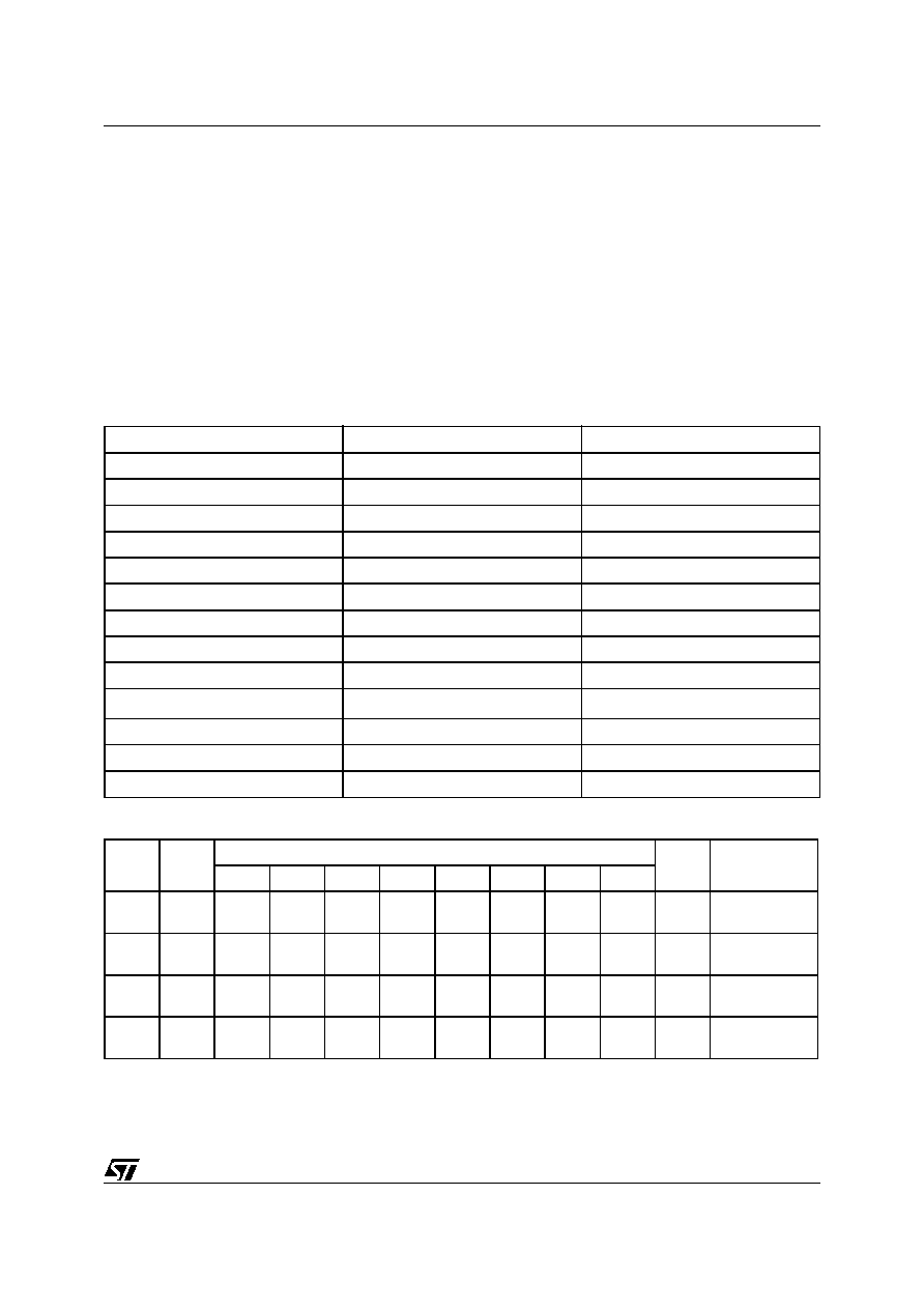
27/129
uPSD33XX
Interrupt Priority Structure
Each interrupt source can be assigned one of two
priority levels. Interrupt priority levels are defined
by the Interrupt Priority special function registers
IP and IPA.
0 = low priority
1 = high priority
A low priority interrupt may be halted by a high pri-
ority level interrupt. A high priority interrupt routine
cannot be halted by any other interrupt source. If
two interrupts of different priority occur simulta-
neously, the higher priority level request is ser-
viced. If requests are of the same priority and are
received simultaneously, an internal polling se-
quence determines which request is serviced.
Thus, within each priority level, there is a second
priority structure determined by the polling se-
quence.
Interrupts Enable Structure
Each interrupt source can be individually enabled
or disabled by setting or clearing a bit in the Inter-
rupt Enable special function register IE and IEA.
All interrupt sources can also be globally disabled
by clearing Bit EA in the IE register.
Table 9. Priority Level
Table 10. Interrupt SFR
Priority
SOURCE
VECTOR ADDRESS
0 (Highest)
DEBUG
0063H
1
ExtINT0
0003H
2
Timer 0
000BH
3
ExtINT1
0013H
4
Timer 1
001BH
5
UART0
0023H
6
Timer 2 + EXF2
002BH
7
SPI
0053H
8
Reserved
0033H
9
I
2
C
0043H
10
ADC
003BH
11
PCA
005BH
12
UART1
004BH
SFR
Addr
Reg
Name
Bit Register Name
Reset
Value
Comments
7
6
5
4
3
2
1
0
A7
IEA
ADC
SPI
PCA
ES1
≠
≠
EI
2
C
00
Interrupt
Enable (2nd)
A8
IE
EA
EDB
ET2
ES0
ET1
EX1
ET0
EX0
00
Interrupt
Enable
B7
IPA
PADC
PSPI
PPCA
PS1
≠
≠
PI
2
C
00
Interrupt
Enable (2nd)
B8
IP
≠
PDB
PT2
PS0
PT1
PX1
PT0
PX0
00
Interrupt
Priority
uPSD33XX
28/129
Table 11. Interrupt Enable SFR IE Bit Definition (A8H)
Table 12. Interrupt Enable Addition SFR IEA Bit Definition (A7H)
Table 13. Interrupt Priority Level SFR IP Bit Definition (B8H)
BIT
SYMBOL
FUNCTION
7
EA
Disable all interrupts.
0 = No interrupt will be acknowledged
1 = Each interrupt source is individually enabled or disabled by setting or clearing its
enable bit.
6
EDB
Debug Unit Interrupt
5
ET2
Enable Timer 2 Interrupt
4
ES0
UART0 Interrupt
3
ET1
Enable Timer 1 Interrupt
2
EX1
Enable External Interrupt (INT1)
1
ET0
Enable Timer 0 Interrupt
0
EX0
Enable External Interrupt (INT0)
BIT
SYMBOL
FUNCTION
7
EADC
ADC Interrupt
6
ESPI
SPI Interrupt
5
EPCA
Programmable Counter Array Interrupt
4
ES1
UART1 Interrupt
3
≠
Reserved
2
≠
Reserved
1
EI
2
C
Enable I
2
C Interrupt
0
≠
Reserved
BIT
SYMBOL
FUNCTION
7
≠
Reserved
6
PDB
Debug Interrupt Level
5
PT2
Timer 2 Interrupt priority level
4
PS0
UART0 Interrupt priority level
3
PT1
Timer 1 Interrupt priority level
2
PX1
External Interrupt (INT1) priority level
1
PT0
Timer 0 Interrupt priority level
0
PX0
External Interrupt (INT0) priority level

29/129
uPSD33XX
Table 14. Interrupt Priority Level Addition SFR IPA Bit Definition (B7H)
POWER SAVINGS MODES
Three software-selectable modes of reduced pow-
er consumption are implemented.
s
Idle Mode
s
Power-down Mode
s
Reduced Frequency Mode
Idle Mode Function Activity
The following functions are switched off when the
microcontroller enters the Idle Mode:
≠ CPU (halted - waiting for interrupt to exit halt)
The following functions remain active during Idle
Mode (except when disabled by the control regis-
ters). Some of these functions may generate an in-
terrupt or reset and thus terminate the Idle Mode.
≠ External Interrupts
≠ Timer 0, Timer 1 and Timer 2
≠ Watchdog Timer
≠ ADC
≠ I
2
C Bus Interface
≠ UART0 and UART1
≠ ADC
≠ SPI
≠ PCA (PWM)
Table 15. Port Status at Power-saving Mode
Table 16. Bus Signals at Power-down and Idle Mode
BIT
SYMBOL
FUNCTION
7
PADC
ADC Interrupt priority level
6
PSPI
SPI Interrupt priority level
5
PPCA
PCA Interrupt level
4
PS1
UART1 Interrupt priority level
3
≠
Not used
2
≠
Not used
1
PI
2
C
I
2
C Interrupt priority level
0
≠
Reserved
Mode
Ports 1, 3, 4
PCA
SPI
I
2
C
ADC
Idle
Maintain Data
Active
Active
Active
Active
Power-down
Maintain Data
Disable
Disable
Disable
Disable
Mode
ALE
PSEN_
RD_
WR_
AD0-7
A8-15
Idle
0
1
1
1
FF
FF
Power-down
0
1
1
1
FF
FF
uPSD33XX
30/129
Idle Mode
The instruction that sets PCON.0 is the last in-
struction executed in the normal operating mode
before Idle Mode is activated. Once in the Idle
Mode, the CPU status is preserved in its entirety:
Stack pointer, Program counter, Program status
word, Accumulator, RAM, and All other registers
maintain their data during Idle Mode.
There are three ways to terminate the Idle Mode:
≠ Activation of any enabled interrupt will cause
PCON.0 to be cleared by hardware,
terminating Idle Mode. The interrupt is
serviced, and following return from interrupt
instruction, RETI, the next instruction to be
executed will be the one which follows the
instruction that wrote a logic '1' to PCON.0.
≠ External hardware reset: the hardware reset
is required to be active for two machine
cycles to complete the RESET operation.
≠ Internal reset: the microcontroller restarts
after 3 machine cycles in all cases.
Power-down Mode
The instruction that sets PCON.1 is the last exe-
cuted prior to going into the Power-down Mode.
Once in Power-down Mode, the oscillator is
stopped. The contents of the on-chip RAM and the
Special Function Register are preserved.
The Power-down Mode can be terminated by an
external RESET.
Table 17. PCON Register Bit Definition (87H, Reset Value 00H)
Note: 1. See the T2CON Register (Table 39, page 44) for details of the flag description.
BIT
SYMBOL
FUNCTION
7
SMOD0
Baud Rate Double Bit (UART0)
0 = No Doubling
1 = Doubling
6
SMOD1
Baud Rate Double Bit for 2nd UART (UART1)
0 = No Doubling
1 = Doubling
5
LVD
Disable LVD by setting this bit.
0 = Enable
1 = Disable
4
POR
Power-on reset sets this bit to '1.' See SUPERVISORY, page 37 for details.
0 = Clear with software
1 = Set by power-on reset generated by Supervisory circuit
3
RCLK1
(1)
Received Clock Flag (UART1)
2
TCLK1
(1)
Transmit Clock Flag (UART1)
1
PD
Activate Power-down Mode
0 = Exit from Power-down
1 = Enter into Power-down
0
IDL
Activate Idle Mode
0 = Exit from Idle Mode
1 = Enter into Idle Mode

31/129
uPSD33XX
REDUCED FREQUENCY MODE
The MCU consumes less power at lower clock fre-
quency than at maximum frequency. The MCU
can reduce the clock frequency by dividing the
f
OSC
with the divider as defined in CCON0 Regis-
ter (see Figure 12). This mode allows the MCU to
remain active while consuming less power at a
slower speed. By changing back to the original di-
vider the MCU returns to normal mode. See
CLOCK GENERATION, page 31 for more infor-
mation.
In Reduced Frequency Mode, the Peripherals can
still be functional at normal f
OSC
frequency.
Figure 12. Clock Generation Logic
Note: 1. XTAL can be divided by 2 to 2048.
CLOCK GENERATION
The clock unit uses the external crystal oscillator
as a reference input clock, whose frequency is de-
noted by F
OSC
. Based on the Frequency Selection
Control registers (CCON0), the clock unit gener-
ates the following clocks:
CPUCLK. A clock for CPU and CPU-tightly-relat-
ed peripherals (e.g., JTAG, WDT, IO_PORT). This
clock is disabled in both the Power-down Mode
and the Idle Mode. The frequency of CPUCLK is
f
CPU
, which is obtained based on the f
OSC
, CP-
UPS[2:0], and internal signals Idle, and Stall.
When 'Idle' is 1, f
CPU
is 0MHz. Otherwise, f
CPU
is
a function of f
OSC
, CPUPS[2:0], and Stall. The
Stall signal is generated from the Pre-fetch Queue
(PFQ) block when the requested program code is
not prepared in PFQ yet. CPUCLK is alive after a
breakpoint match or when the CPU is put in the
halt state by the Debug Unit.
CPUCLK_nonstop. A clock for CPU-loosely-re-
lated peripherals (e.g., Debug, Interrupt). This
clock is the same as CPUCLK, except this clock is
alive in Idle Mode.
PFQCLK. A clock for PFQ. This clock is same as
CPUCLK except that this is alive even in Idle Mode
or when the CPU is stalled.
OSCCLK. A clock for non-CPU related peripher-
als (e.g., TIMER0/1/2, UART0/1, PCA0/1, SPI).
The frequency of OSCCLK is f
OSC
, which is ob-
tained from the external clock input. This clock is
disabled only in the Power-down Mode.
The clock status is summarized in Table 18, page
32.
XT AL1
CPUPS
Buffer
Q
Q
Q
MUX
PCON[0]: IDLE
CP UCLK
(CPU, WDT, IO_PORT)
CP UCLK_nonstop
(DBG, IRU)
OSCCLK
(TIMER0/1/2, UART0/1,
P CA0/1, SP I,ADC)
PCON[1] : Power Down
XTAL1
[Clock Divider]
STALL
P FQCLK
(PFQ)
CP U CLK_muxout
XTAL1 / 2
XTAL1 / 4
XTAL1 / 2048
∑
∑
∑
AI07845
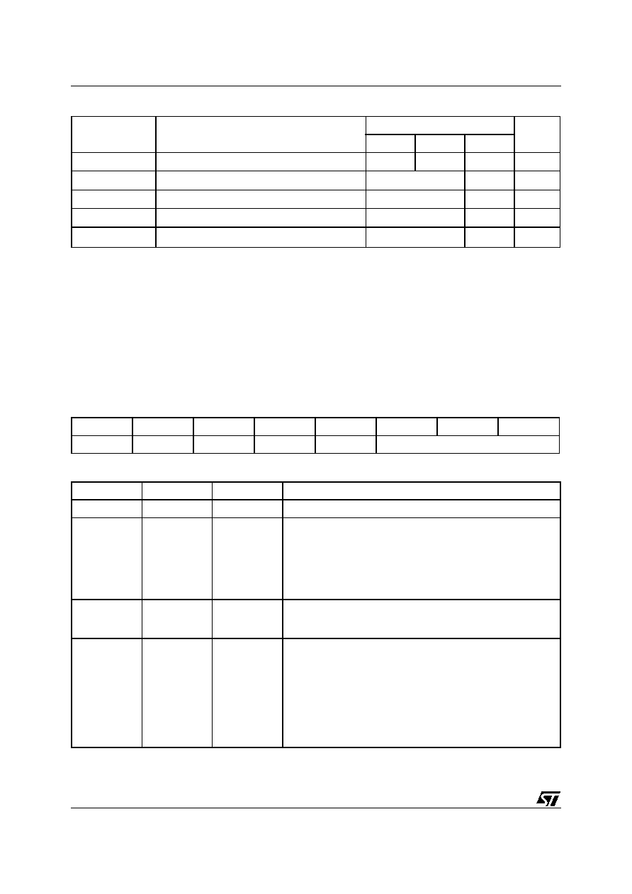
uPSD33XX
32/129
Table 18. Clock Status
Note: 1. OSCCLK is the output of the crystal oscillator.
CPU CLOCK CONTROL REGISTER
The CPU Clock frequency is controlled by the
CCON0 Register. The CPU is running at full fre-
quency at power-up. The CPU Clock frequency
can be changed any time by writing to the CPUPS
Bits in the CCON0 register. After writing to the
CCON0, the CPU Clock will be switched to the
new frequency immediately. The CPU Clock can
be reduced by dividing the f
OSC
by 2 to 2048.
When the CPU is running at reduced clock fre-
quency and the CPUAR Bit is set, it allows the
CPU Clock to return to full frequency immediately
when any interrupt occurs. This is achieved by au-
tomatically changing the CPUPS Bits to '000.'
Table 19. CCON0 Register Bit Definition (0F9H, Reset Value 10H)
Table 20. CCON0 Register Bit Definition Details
Name
Modules
Power-saving Modes
Freq.
NORMAL
IDLE
PD
CPUCLK
CPU, JTAG, WDT, IO_PORT
ON
OFF
OFF
f
CPU
CPUCLK_nonstop
Debug, Interrupt
ON
OFF
f
CPU
PFQCLK
PFQ
ON
OFF
f
CPU
JTAGCLK
JTAG
ON
OFF
f
JTAG
OSCCLK
(1)
TIMER0/1/2, UART0/1, PCA0/1, SPI, I
2
C, ADC
ON
OFF
f
OSC
Bit 7
Bit 6
Bit 5
Bit 4
Bit 3
Bit 2
Bit 1
Bit 0
Reserved
Reserved
Reserved
DBGCE
CUPAR
CPUPS[2:0]
BIT
SYMBOL
RW
Definition
7-5
≠
Reserved
4
DBGCE
RW
Debug Address Comparison Enable
0 = DBG Address Comparison is disabled
1 = DBG Address Comparison is enabled (Default during the reset
period.)
After reset, this bit is set to enable the Debug Unit's Address
Comparison feature for debugging purposes. This bit should be
set to '0' if the debugging function is not needed.
3
CPUAR
RW
Automatic CPU Clock Recovery
0 = There is no change of CPUPS[2:0] when an interrupt occurs.
1 = CPUPS[2:0] becomes 3'b000 whenever any interrupt occurs.
2:0
CPUPS
RW
CPUCLK Pre-Scaler
000: f
CPU
= f
OSC
(Default during the reset period)
001: f
CPU
= f
OSC
/2
010: f
CPU
= f
OSC
/4
011: f
CPU
= f
OSC
/8
100: f
CPU
= f
OSC
/16
101: f
CPU
= f
OSC
/32
110: f
CPU
= f
OSC
/1024
111: f
CPU
= f
OSC
/2048

33/129
uPSD33XX
OSCILLATOR
The oscillator circuit of the uPSD33XX Devices is
a single stage, inverting amplifier in a Pierce oscil-
lator configuration. The circuitry between XTAL1
and XTAL2 is basically an inverter biased to the
transfer point. Either a crystal or ceramic resonator
can be used as the feedback element to complete
the oscillator circuit. Both are operated in parallel
resonance. XTAL1 is the high gain amplifier input,
and XTAL2 is the output. To drive the uPSD33XX
Devices externally, XTAL1 is driven from an exter-
nal source and XTAL2 left open-circuit.
The uPSD33XX can run at maximum 40MHz
clock. The CPU clock frequency can be configured
in the CCON0 Register. However, the I
2
C bus re-
quires a minimum 8MHz clock to be functional.
Figure 13. Oscillator
I/O PORTS (MCU MODULE)
The MCU Module has three ports: Port 1, Port 3,
and Port 4 (see Table 21). (Refer to the PSD
MODULE, page 71 and I/O PORTS (PSD MOD-
ULE), page 90). The ports support:
s
General Purpose I/O
s
Alternate peripheral functions
s
5V tolerant
s
High current on Port 4
The 80-pin uPSD33XX also has two ports in the
MCU Module that are dedicated for the external
MCU address and data bus. Ports 1, 3, and 4 are
the same as in the standard 8032 microcontrollers,
with the exception of the additional special periph-
eral functions. All ports are bi-directional. Pins
which are not configured as Alternate functions
are normally bi-directional I/O.
The following SFR registers are used to control the
mapping of alternate functions onto the I/O Port
Bits (see Table 22 and Table 23). Port 1 and 4 al-
ternate functions are controlled using the PXSFS1
registers. Port 3 alternate functions are controlled
using the P3SFS register. After reset, the port SFR
registers are cleared and are defaulted to general
I/O.
Table 21. I/O Port Functions
AI06620
XTAL1
XTAL2
8 to 40 MHz
XTAL1
XTAL2
External Clock
Port Name
General Purpose I/O
Alternate 1 Function
Alternate 2 Function
Port 1
GPIO
Timer 2 - Pins 0, 1
UART1 - Pins 2, 3
SPI - Pins 4.. 7
ADC - PIns 0.. 7
Port 3
GPIO
UART0 - Pins 0, 1
Interrupt - Pins 2, 3
Timers - Pins 4, 5
I
2
C - Pins 6, 7
None
Port 4
GPIO
PCA0 - Pins 0.. 3
PCA1 - Pins 4-7
Timer 2 - Pins 0, 1
UART1 - Pins 2.. 3
SPI - Pins 4.. 7

uPSD33XX
34/129
Port 1 Register P1SFS0, Port 1 Register P1SFS1
P1SFS0 Register Bits 0.. 7 definition (see Table
22):
0 = Select pin as GPIO
1 = Select pin as Alternate function
When the bit in the P1SFS0 register is '1,' alter-
nate peripheral functions are assigned to the pin.
The new P1SFS1 register bit further selects which
one of the alternate function to be enabled. Table
23 shows the alternate functions assigned to port
1 and how it can be selected.
Table 22. Port 1 Register P1SFS0 (8EH, Reset Value 00H)
Table 23. Port 1 Register P1SFS1 (8FH, Reset Value 00H)
Port 3 Configuration Register
Port 3 configuration is compatible to standard
8032, including alternate function pin assignments
as shown in Table 24.
Port 4 Configuration Register
Port 4 has two registers: P4SFS0 Bit = 0 config-
ures pin as GPIO and Bit = 1 configures pin as al-
ternate function. P4SFS1 Bit determines which
alternate function is to be enabled (see Table 25).
The alternate 2 functions on Port 4 are the same
as the alternate function 1 of Port 1. If an identical
alternate function is assigned to both ports, the
Port 1 function has priority and the Port 4 function
is disabled.
P4SFS0 Register Bits 0.. 7 definition:
0 = Select pin as GPIO
1 = Select pin as Alternate function
Port 4 High Current Option
Port 4 is a high current port (see Table 26). All 8 of
the port pins are capable of a sink/source value of
10mA per pin in alternative function mode. The
pins can sink 10mA in GPIO Mode. See the DC
AND AC PARAMETERS, page 104, for V
OL
/V
OH
specification on Port 4.
Table 24. Port 3 Register P3SFS (91H, Reset Value 00H)
Table 25. Port 4 Register P4SFS0 (92H, Reset Value 00H)
Table 26. Port 4 Register P4SFS1 (93H, Reset Value 00H)
Bit 7
Bit 6
Bit 5
Bit 4
Bit 3
Bit 2
Bit 1
Bit 0
0 = Port 1.7
1 = Alternate
0 = Port 1.6
1 = Alternate
0 = Port 1.5
1 = Alternate
0 = Port 1.4
1 = Alternate
0 = Port 1.3
1 = Alternate
0 = Port 1.2
1 = Alternate
0 = Port 1.1
1 = Alternate
0 = Port 1.0
1 = Alternate
Bit 7
Bit 6
Bit 5
Bit 4
Bit 3
Bit 2
Bit 1
Bit 0
0 = Alternate1
1 = Alternate2
0 = Alternate1
1 = Alternate2
0 = Alternate1
1 = Alternate2
0 = Alternate1
1 = Alternate2
0 = Alternate1
1 = Alternate2
0 = Alternate1
1 = Alternate2
0 = Alternate1
1 = Alternate2
0 = Alternate1
1 = Alternate2
Bit 7
Bit 6
Bit 5
Bit 4
Bit 3
Bit 2
Bit 1
Bit 0
0 = Port 3.7
1 = Alternate
0 = Port 3.6
1 = Alternate
0 = Port 3.5
1 = Alternate
0 = Port 3.4
1 = Alternate
0 = Port 3.3
1 = Alternate
0 = Port 3.2
1 = Alternate
0 = Port 3.1
1 = Alternate
0 = Port 3.0
1 = Alternate
Bit 7
Bit 6
Bit 5
Bit 4
Bit 3
Bit 2
Bit 1
Bit 0
0 = Port 4.7
1 = Alternate
0 = Port 4.6
1 = Alternate
0 = Port 4.5
1 = Alternate
0 = Port 4.4
1 = Alternate
0 = Port 4.3
1 = Alternate
0 = Port 4.2
1 = Alternate
0 = Port 4.1
1 = Alternate
0 = Port 4.0
1 = Alternate
Bit 7
Bit 6
Bit 5
Bit 4
Bit 3
Bit 2
Bit 1
Bit 0
0 = Alternate1
1 = Alternate2
0 = Alternate1
1 = Alternate2
0 = Alternate1
1 = Alternate2
0 = Alternate1
1 = Alternate2
0 = Alternate1
1 = Alternate2
0 = Alternate1
1 = Alternate2
0 = Alternate1
1 = Alternate2
0 = Alternate1
1 = Alternate2

35/129
uPSD33XX
MCU MEMORY BUS INTERFACE
The MCU Module reads or writes to the PSD Mod-
ule through the MCU memory bus. The Memory
Bus is also available to external pins in the 80-pin
package. The 8-bit MCU bus consists of standard
8032 bus signals.
READ Bus Cycle (Code or XDATA)
The READ bus cycle reads 8 bits per bus cycle
and is identical for both the Program Fetch (PSEN)
and Data Read (RD) in terms of timing and func-
tion. When the PSD Module is selected and either
PSEN or RD is active, the PSD Module will drive
data D0-D7 of the MCU bus. For program fetch,
the MCU keeps the byte in the Pre-fetch Buffer. As
for the XDATA READ bus cycle, the MCU routes
the data byte to the CPU core directly. The READ
bus cycle timing and length is controlled by the
BUSCON Register.
WRITE Bus Cycle (XDATA)
The MCU writes one byte per bus cycle. The tim-
ing and length of the WRITE Bus Cycle is con-
trolled by the BUSCON Register, which can be
programmed by the software.
Bus Control Register (BUSCON)
The uPSD33XX has a programmable bus inter-
face where the user can specify the length of a bus
cycle. Based on the PQF Clock frequency, the
number of clocks in a bus cycle can be changed to
maximize data transfer rate (see Table 28). The
uPSD33XX defaults to 6 PFQ clock for all READ
and WRITE bus cycles after reset. Table 29 shows
the minimum number of PFQ clocks in a bus cycle
that are required for different PFQ Clock frequen-
cies.
In addition, the BUSCON allows the user to set
bits to turn on/off the Prefetch Queue and Branch
Cache. In some real time applications, turning off
the queue and cache provides determinable exe-
cution. The user may also wish to turn the queue
and cache off during debugging.
Table 27. BUSCON Register Bit Definition (9DH, Reset Value 2BH)
Table 28. Number of PFQ Clocks Required to Optimize Bus Transfer Rate
Note: 1. V
DD
of the PSD Module
Bit 7
Bit 6
Bit 5
Bit 4
Bit 3
Bit 2
Bit 1
Bit 0
EPFQ
EBC
WRW1
WRW0
RDW1
RDW0
CW1
CW0
PFQ Clock
Frequency
Code Data
READ Data
WRITE Data
3V
(1)
5V
(1)
3V
(1)
5V
(1)
3V
(1)
5V
(1)
25-40MHz
5
4
5
4
5
4
8-24MHz
3
3
4
4
4
4

uPSD33XX
36/129
Table 29. BUSCON Register Bit Definition Details
Register Bit
Definition
CW1.. CW0
Code Fetch bus cycle:
When PFQ fetches code,
2'b00: The code read from memory takes 3 PFQCLK clocks
2'b01: The code read from memory takes 4 PFQCLK clocks
2'b10: The code read from memory takes 5 PFQCLK clocks
2'b11: The code read from memory takes 6 PFQCLK clocks (default)
RDW1.. RDW0
XDATA READ bus cycle:
2'b00: The code read from XDATA takes 4 PFQCLK clocks
2'b01: The code read from XDATA takes 5 PFQCLK clocks
2'b10: The code read from XDATA takes 6 PFQCLK clocks (default)
2'b11: The code read from XDATA takes 7 PFQCLK clocks
WRW1.. WRW0
XDATA WRITE bus cycle
2'b00: The code read from XDATA takes 4 PFQCLK clocks
2'b01: The code read from XDATA takes 5 PFQCLK clocks
2'b10: The code read from XDATA takes 6 PFQCLK clocks (default)
2'b11: The code read from XDATA takes 7 PFQCLK clocks
EBC
Enable Branch Cache
0 = BC is disabled (default)
1 = BC is enabled
EPFQ
Enable Prefetch Queue
0 = PFQ is disabled (default)
1 = PFQ is enabled

37/129
uPSD33XX
SUPERVISORY
There are four ways to invoke a reset and initialize
the uPSD33XX Devices:
s
Via the external RESET pin
s
Via the internal LVR Block.
s
Via Watch Dog timer
Each RESET source will cause an internal reset
signal to be active. The CPU responds by execut-
ing an internal reset and puts the internal registers
in a defined state. This internal reset is also routed
as an active low reset input to the PSD Module.
Figure 14. RESET Configuration
Note: 1. 10ms at 40MHz, 50ms at 8MHz.
External Reset
The RESET pin is connected to a Schmitt trigger
for noise reduction. A RESET is accomplished by
holding the RESET pin LOW for at least 1ms at
power-up while the oscillator is running. Refer to
AC specification on other RESET timing require-
ments.
Low V
CC
Voltage Reset
An internal reset is generated by the LVR circuit
when the V
CC
drops below the reset threshold. Af-
ter V
CC
returns to the reset threshold, the RESET
signal will remain asserted for 10ms before it is re-
leased. On initial power-up the LVR is enabled
(default). After power-up the LVR can be disabled
via the LVREN Bit in the PCON Register.
Note: The LVR logic is functional in both the Idle
and Power-down Modes. The reset circuit resides
in the MCU Module which operates at 3.3V V
CC
.
The reset threshold will always be: 2.5V +/-0.2V
for all uPSD33XX devices.
This logic supports approximately 0.1V of hystere-
sis and 1µs noise-cancelling delay.
Watchdog Timer Overflow Reset
The Watchdog timer generates an internal reset
when its 24-bit counter overflows. See WATCH-
DOG TIMER, page 38 for details.
Debug Unit Reset
The Debug Unit can generate a reset to the Super-
visory circuit for debugging purpose. Under normal
operation, this reset source is disabled.
Reset Output
The output of the reset logic resets the MCU, it
also drives a PSD_Reset signal (active low) which
is connected to the Reset Input on the PSD Mod-
ule. The output of the reset logic remains asserted
for a minimum of approximately 10ms. This time
base is calculated by counting the f
OSC
at 40Mhz
to last a minimum of 10ms at 40Mhz. The time will
be longer as the f
OSC
is lower.
Power-up Reset
At power up, the internal reset generated by the
LVD circuit is latched as a '1' in the PCON register
(Bit POR). Software can read this bit and deter-
mine whether the last CPU reset is a power up or
warm reset. This bit must be cleared with software.
RESET
Input Pin
CPU
&
PERI.
Noise
Cancel
LVR
S
Q
R
CPU
Clock
Sync
10ms
(1)
Timer
WDT
PSD_RST
"Active Low signal"
Debug
AI07849
uPSD33XX
38/129
WATCHDOG TIMER
The hardware watchdog timer (WDT) resets the
uPSD33XX Devices when it overflows. The WDT
is intended as a recovery method in situations
where the CPU may be subjected to a software
upset. To prevent a system reset the timer must be
reloaded in time by the application software. If the
processor suffers a hardware/software malfunc-
tion, the software will fail to reload the timer. This
failure will result in a reset upon overflow thus pre-
venting the processor running out of control.
In the Idle Mode the watchdog timer and reset cir-
cuitry remain active. The WDT consists of a 24-bit
counter, the Watchdog Timer RESET (WDRST)
SFR, and the Watchdog Key Register (WDKEY).
Since the WDKEY register is loaded with 55h after
reset, the Watchdog is disabled until it is enabled
by the software.
Watchdog Counter
The 24-bit counter runs on machine cycle (4 f
OSC
clocks) and has a WDT reset period of about 1.6
seconds (see Figure 15). The 8th MSB of the
counter is loaded from the Watch Dog Timer Clear
Register (WDRST). By writing to the WDRST reg-
ister, the user can change the WDT reset period.
The 24-bit counter overflows when it reaches
FFFFFFh.
Figure 15. Watchdog Counter
T
STALL
: the average waiting time due to PFQ/BC stall
For example, when t
STALL
is '0' and t
OSC
is 25ns, the total required cycle (to reach the overflow of the 24-
bit counter that is clocked at machine cycle) is as below:
Therefore, the reset period is:
8 bit
8 bit
8 bit
WDTRST
23
15
7
0
AI07850
m ach in e cycl e
4T
OSC
T
STALL
+
(
)
wh ere T
OSC
,
1
40M Hz
--------------------
0.025 us
25ns
=
=
=
=
2
24
2
2
◊
2
26
2
6
2
20
◊
64
2
10
(
)
2
◊
=
64 m il li on
O SCcycl e
(
)
=
=
=
rese t p erio d
64M
25n s
1.6 s
=
◊
=

39/129
uPSD33XX
WDT Registers
WDTKEY Register
≠ When this SFR is written as #55h, the WDT is
disabled. Otherwise, writing any other values
to the register will disable the WDT. Since the
reset value of WDTKEY is #55h, the WDT is
disabled at reset. The WDT is disabled after
the reset that is generated by the WDT
counter overflow.
≠ When the WDT is disabled, the 24-bit counter
is cleared. Therefore, the new value of
WDTRST must be written into the 24-bit
counter after the WDT is enabled.
≠ In Idle Mode, the oscillator continues to run.
To prevent the WDT from resetting the
processor while in Idle, the user should
always set up a timer that will periodically exit
Idle, service the WDT, and re-enter Idle
Mode.
WDTRST Register
≠ When this SFR is written as a value, the value
is loaded into the upper 8 bits of 24-bit
counter in WDT. And, the lower 16 bits are
cleared.
≠ If the user write "WDTRST" by '04h, then the
value of the 24-bit counter changes from
040000, 040001, 040002, ..., FFFFFF, then
generates the WDT reset.
Table 30. WDKEY: Watchdog Timer Key Register (0AEH, Reset Value 55H)
Table 31. WDKEY: Watchdog Timer Key Register Details
Table 32. WDRST: Watchdog Timer Clear Register (0A6H, Reset Value 00H)
Table 33. WDRST: Watchdog Timer Clear Register Details
Bit 7
Bit 6
Bit 5
Bit 4
Bit 3
Bit 2
Bit 1
Bit 0
WDKEY7
WDKEY6
WDKEY5
WDKEY4
WDKEY3
WDKEY2
WDKEY1
WDKEY0
Register Bit
Definition
WDKEY7.. 0
Enable or disable watchdog timer. Writing to WDKEY with data pattern 01010101 (= 55h)
will disable the watchdog timer. Other data: enables the watchdog timer.
Bit 7
Bit 6
Bit 5
Bit 4
Bit 3
Bit 2
Bit 1
Bit 0
WDRST7
WDRST6
WDRST5
WDRST4
WDRST3
WDRST2
WDRST1
WDRST0
Register Bit
Definition
WDRST[7.. 0]
To reset watchdog timer, write any value to this register. This value is loaded to the 8th
most significant bits of the 24-bit counter.

uPSD33XX
40/129
TIMER/COUNTERS (TIMER0, TIMER1, AND TIMER 2)
The uPSD33XX Devices has three 16-bit Timer/
Counter registers: Timer 0, Timer 1 and Timer 2.
All of them can be configured to operate either as
timers or event counters and are compatible with
standard 8032 architecture (see Table 34).
In the "Timer" function, the register is incremented
every 1/12 of the oscillator frequency (f
OSC
).
In the "Counter" function, the register is increment-
ed in response to a 1-to-0 transition at its corre-
sponding external input pin, T0 or T1. In this
function, the external input is sampled by the
counter. When the samples show a high in one
machine cycle and a low in the another, the count
is incremented. The new count value appears in
the register during the cycle following the one in
which the transition was detected. The maximum
count rate is 1/24 of the f
OSC
as in standard 8032.
There are no restrictions on the duty cycle of the
external input signal, but to ensure that a given
level is sampled at least once before it changes, it
should be held for at least one full machine cycle.
In addition to the "Timer" or "Counter" selection,
Timer 0 and Timer 1 have four operating modes
from which to select.
Timer 0 and Timer 1
The "Timer" or "Counter" function is selected by
control bits C/T in the Special Function Register,
TMOD (see Table 35). These Timer/Counters
have four operating modes, which are selected by
bit-pairs (M1, M0) in TMOD. Modes 0, 1, and 2 are
the same for Timers/ Counters. Mode 3 is differ-
ent.
Table 34. TCON Register (88H, Reset Value 00H) - Timer 0, 1
Table 35. TCON Register Details - Timer 0, 1
Bit 7
Bit 6
Bit 5
Bit 4
Bit 3
Bit 2
Bit 1
Bit 0
TF1
TR1
TF0
TR0
IE1
IT1
IE0
IT0
Bit
Symbol
Function
7
TF1
Timer 1 Overflow flag. Set by hardware on Timer/Counter overflow. Cleared by
hardware when processor vectors to interrupt routine
6
TR1
Timer 1 Run Control Bit. Set/cleared with software to turn Timer/Counter on or off
5
TF0
Timer 0 Overflow flag. Set by hardier on Timer/Counter overflow. Cleared by hardware
when processor vectors to interrupt routine
4
TR0
Timer 0 Run Control Bit. Set/cleared with software to turn Timer/Counter on or off
3
IE1
Interrupt 1 Edge flag. Set by hardware when external interrupt edge detected. Cleared
when interrupt processed
2
IT1
Interrupt 1 Type Control Bit. Set/cleared with software to specify falling-edge/low-level
triggered external interrupt
1
IE0
Interrupt 0 Edge flag. Set by hardware when external interrupt edge detected. Cleared
when interrupt processed
0
IT0
Interrupt 0 Type Control Bit. Set/cleared with software to specify falling-edge/low-level
triggered external interrupt

41/129
uPSD33XX
Mode 0. Putting either Timer into Mode 0 makes
it look like an 8048 Timer, which is an 8-bit Counter
with a divide-by-32 prescaler. Figure 16 shows the
Mode 0 operation as it applies to Timer 1.
In this mode, the Timer register is configured as a
13-bit register. As the count rolls over from all '1s'
to all '0s,' it sets the Timer Interrupt flag TF1. The
counted input is enabled to the Timer when
TR1 = 1 and either GATE = 0 or /INT1 = 1. (Setting
GATE = 1 allows the Timer to be controlled by ex-
ternal input /INT1 to facilitate pulse width mea-
surements). TR1 is a control bit in the Special
Function Register TCON (TCON Control Regis-
ter). GATE is in TMOD (see Table 36 and Table
37, page 43).
The 13-bit register consists of all 8 bits of TH1 and
the lower 5 bits of TL1. The upper 3 bits of TL1 are
indeterminate and should be ignored. Setting the
run flag does not clear the registers.
Mode 0 operation is the same for the Timer 0 as
for Timer 1. Substitute TR0, TF0, and /INT0 for the
corresponding Timer 1 signals in Figure 16. There
are two different GATE Bits, one for Timer 1 and
one for Timer 0.
Mode 1. Mode 1 is the same as Mode 0, except
that the Timer register is being run with all 16 bits.
Mode 2. Mode 2 configures the Timer register as
an 8-bit Counter (TL1) with automatic reload, as
shown in Figure 17, page 42. Overflow from TL1
not only sets TF1, but also reloads TL1 with the
contents of TH1, which is preset with software.
The reload leaves TH1 unchanged. Mode 2 oper-
ation is the same for Timer/Counter 0.
Mode 3. Timer 1 in Mode 3 simply holds its count.
The effect is the same as setting TR1 = 0.
Timer 0 in Mode 3 establishes TL0 and TH0 as two
separate counters. The logic for Mode 3 on Timer
0 is shown in Figure 18. TL0 uses the Timer 0 con-
trol Bits: C/T, GATE, TR0, INT0, and TF0. TH0 is
locked into a timer function (counting machine cy-
cles) and takes over the use of TR1 and TF1 from
Timer 1. Thus, TH0 now controls the "Timer 1"In-
terrupt.
Mode 3 is provided for applications requiring an
extra 8-bit timer on the counter (see Figure 18,
page 42). With Timer 0 in Mode 3, an uPSD33XX
Devices can look like it has three Timer/Counters.
When Timer 0 is in Mode 3, Timer 1 can be turned
on and off by switching it out of and into its own
Mode 3, or can still be used by the serial port as a
baud rate generator, or in fact, in any application
not requiring an interrupt.
Figure 16. Timer/Counter Mode 0: 13-bit Counter
AI06622
f
OSC
TF1
Interrupt
Gate
TR1
INT1 pin
T1 pin
Control
TL1
(5 bits)
TH1
(8 bits)
C/T = 0
C/T = 1
˜ 12

uPSD33XX
42/129
Figure 17. Timer/Counter Mode 2: 8-bit Auto-reload
Figure 18. Timer/Counter Mode 3: Two 8-bit Counters
AI06623
f
OSC
TF1
Interrupt
Gate
TR1
INT1 pin
T1 pin
Control
TL1
(8 bits)
TH1
(8 bits)
C/T = 0
C/T = 1
˜ 12
AI06624
f
OSC
TF0
Interrupt
Gate
TR0
INT0 pin
T0 pin
Control
TL0
(8 bits)
C/T = 0
C/T = 1
˜ 12
f
OSC
TF1
Interrupt
Control
TH0
(8 bits)
˜ 12
TR1

43/129
uPSD33XX
Table 36. TMOD Register (TMOD)
Table 37. TMOD Register Details
Timer 2
Like Timers 0 and 1, Timer 2 can operate as either
an event timer or as an event counter. This is se-
lected by Bit C/T2 in the special function register
T2CON. It has three operating modes: capture,
autoload, and baud rate generator, which are se-
lected by bits in the T2CON as shown in Table 38
and Table 39, page 44. In the Capture Mode there
are two options which are selected by Bit EXEN2
in T2CON. If EXEN2 = 0, then Timer 2 is a 16-bit
timer or counter which upon overflowing sets Bit
TF2, the Timer 2 Overflow Bit, which can be used
to generate an interrupt. If EXEN2 = 1, then Timer
2 still does the above, but with the added feature
that a 1-to-0 transition at external input T2EX
causes the current value in the Timer 2 registers,
TL2 and TH2, to be captured into registers
RCAP2L and RCAP2H, respectively. In addition,
the transition at T2EX causes Bit EXF2 in T2CON
to be set, and EXF2 like TF2 can generate an in-
terrupt. The Capture Mode is illustrated in Figure
19, page 45.
In the Auto-reload Mode, there are again two op-
tions, which are selected by bit EXEN2 in T2CON
(see Table 40, page 45). If EXEN2 = 0, then when
Timer 2 rolls over it not only sets TF2 but also
causes the Timer 2 registers to be reloaded with
the 16-bit value in registers RCAP2L and
RCAP2H, which are preset with software. If
EXEN2 = 1, then Timer 2 still does the above, but
with the added feature that a 1-to-0 transition at
external input T2EX will also trigger the 16-bit re-
load and set EXF2. The Auto-reload Mode is illus-
trated in Standard Serial Interface (UART) Figure
20, page 46. The Baud Rate Generation Mode is
selected by (RCLK, RCLK1)=1 and/or (TCLK,
TCLK1)=1. It will be described in conjunction with
the serial port.
Bit 7
Bit 6
Bit 5
Bit 4
Bit 3
Bit 2
Bit 1
Bit 0
GATE
C/T
M1
M0
GATE
C/T
M1
M0
Bit
Symbol
Timer
Function
7
GATE
Timer 1
Gating control when set. Timer/Counter 1 is enabled only while INT1 pin is High and
TR1 control pin is set. When cleared, Timer 1 is enabled whenever TR1 Control Bit is
set
6
C/T
Timer or Counter selector, cleared for timer operation (input from internal system clock);
set for counter operation (input from T1 input pin)
5
M1
(M1,M0)=(0,0): 13-bit Timer/Counter, TH1, with TL1 as 5-bit prescaler
(M1,M0)=(0,1): 16-bit Timer/Counter. TH1 and TL1 are cascaded. There is no prescaler.
(M1,M0)=(1,0): 8-bit auto-reload Timer/Counter. TH1 holds a value which is to be
reloaded into TL1 each time it overflows
(M1,M0)=(1,1): Timer/Counter 1 stopped
4
M0
3
GATE
Timer 0
Gating control when set. Timer/Counter 0 is enabled only while INT0 pin is High and
TR0 control pin is set. When cleared, Timer 0 is enabled whenever TR0 Control Bit is
set
2
C/T
Timer or Counter selector, cleared for timer operation (input from internal system clock);
set for counter operation (input from T0 input pin)
1
M1
(M1,M0)=(0,0): 13-bit Timer/Counter, TH0, with TL0 as 5-bit prescaler
(M1,M0)=(0,1): 16-bit Timer/Counter. TH0 and TL0 are cascaded. There is no prescaler.
(M1,M0)=(1,0): 8-bit auto-reload Timer/Counter. TH0 holds a value which is to be
reloaded into TL0 each time it overflows
(M1,M0)=(1,1): TL0 is an 8-bit Timer/Counter controlled by the standard TImer 0 control
bits. TH0 is an 8-bit timer only controlled by Timer 1 Control Bits
0
M0

uPSD33XX
44/129
Table 38. T2CON: Timer/Counter 2 Control Register (C8H, Reset Value 00H))
Table 39. T2CON Register Details
Note: 1. The RCLK1 and TCLK1 Bits in the PCON Register control UART1, and have the same function as RCLK and TCLK.
Bit 7
Bit 6
Bit 5
Bit 4
Bit 3
Bit 2
Bit 1
Bit 0
TF2
EXF2
RCLK
TCLK
EXEN2
TR2
C/T2
CP/RL2
Bit
Symbol
Function
7
TF2
Timer 2 Overflow flag. Set by a Timer 2 overflow, and must be cleared with software.
TF2 will not be set when either (RCLK, RCLK1)=1 or (TCLK, TCLK)=1
6
EXF2
Timer 2 external flag set when either a capture or reload is caused by a negative
transition on T2EX and EXEN2=1. When Timer 2 Interrupt is enabled, EXF2=1 will
cause the CPU to vector to the Timer 2 Interrupt routine. EXF2 must be cleared with
software
5
RCLK
(1)
Receive Clock flag (UART0). When set, causes the serial port to use Timer 2 overflow
pulses for its receive clock in Modes 1 and 3. TCLK=0 causes Timer 1 overflow to be
used for the receive clock
4
TCLK
(1)
Transmit Clock flag (UART0). When set, causes the serial port to use Timer 2 overflow
pulses for its transmit clock in Modes 1 and 3. TCLK=0 causes Timer 1 overflow to be
used for the transmit clock
3
EXEN2
Timer 2 External Enable flag. When set, allows a capture or reload to occur as a result
of a negative transition on T2EX if Timer 2 is not being used to clock the serial port.
EXEN2=0 causes Time 2 to ignore events at T2EX
2
TR2
Start/Stop control for Timer 2. A logic 1 starts the timer
1
C/T2
Timer or Counter Select for Timer 2. Cleared for timer operation (input from internal
system clock, t
CPU
); set for external event counter operation (negative edge triggered)
0
CP/RL2
Capture/Reload flag. When set, capture will occur on negative transition of T2EX if
EXEN2=1. When cleared, auto-reload will occur either with TImer 2 overflows, or
negative transitions of T2EX when EXEN2=1. When either (RCLK, RCLK1)=1 or (TCLK,
TCLK1)=1, this bit is ignored, and timer is forced to auto-reload on Timer 2 overflow
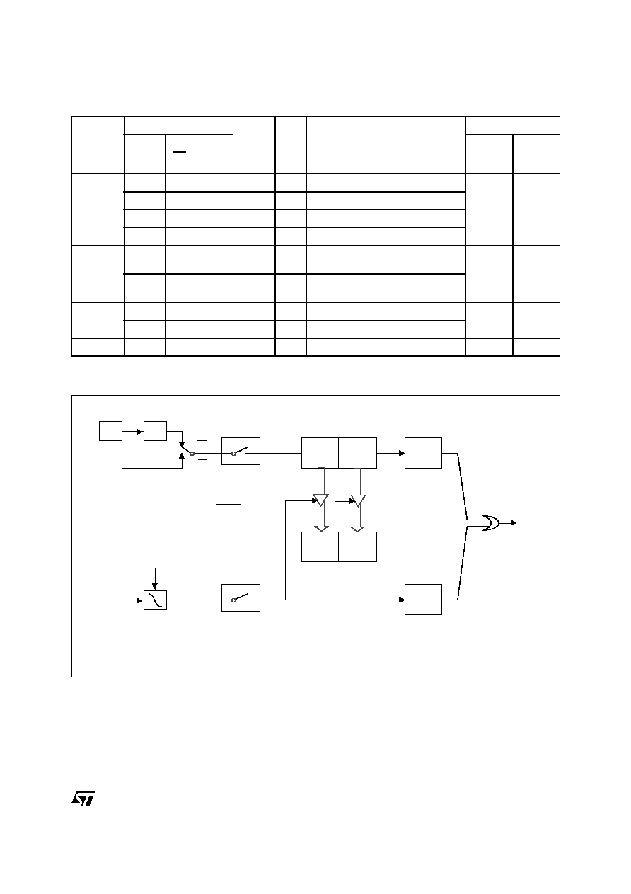
45/129
uPSD33XX
Table 40. Timer/Counter 2 Operating Modes
Note:
= falling edge
Figure 19. Timer 2 in Capture Mode
Mode
T2CON
T2CON
EXEN
P1.1
T2EX
Remarks
Input Clock
RxCLK
or
TxCLK
CP/
RL2
TR2
Internal
External
(P1.0/T2)
16-bit
Auto-
reload
0
0
1
0
x
reload upon overflow
f
OSC
/12
MAX
f
OSC
/24
0
0
1
1
reload trigger (falling edge)
0
0
1
x
0
Down counting
0
0
1
x
1
Up counting
16-bit
Capture
0
1
1
0
x
16-bit Timer/Counter (only up
counting)
f
OSC
/12
MAX
f
OSC
/24
0
1
1
1
Capture (TH2,TL2)
(RCAP2H,RCAP2L)
Baud Rate
Generator
1
x
1
0
x
No overflow interrupt request (TF2)
f
OSC
/12
MAX
f
OSC
/24
1
x
1
1
Extra External Interrupt (Timer 2)
Off
x
x
0
x
x
Timer 2 stops
--
--
AI06625
f
OSC
TF2
Capture
TR2
T2 pin
Control
TL2
(8 bits)
TH2
(8 bits)
C/T2 = 0
C/T2 = 1
˜ 12
EXP2
Control
EXEN2
RCAP2L RCAP2H
T2EX pin
Timer 2
Interrupt
Transition
Detector
uPSD33XX
46/129
Figure 20. Timer 2 in Auto-Reload Mode
AI06626
f
OSC
TF2
Reload
TR2
T2 pin
Control
TL2
(8 bits)
TH2
(8 bits)
C/T2 = 0
C/T2 = 1
˜ 12
EXP2
Control
EXEN2
RCAP2L RCAP2H
T2EX pin
Timer 2
Interrupt
Transition
Detector

47/129
uPSD33XX
STANDARD SERIAL INTERFACE (UART)
The uPSD33XX Devices provide two standard
8032 UART serial ports. The first port (UART0) is
connected to pin P3.0 (RxD0) and P3.1 (TxD0).
The second port (UART1) is connected to pin P1.2
(RxD1) and P1.3(TxD1) or P4.2 and P4.3. The op-
eration of the two serial ports are the same and are
controlled by the SCON0 and SCON1 registers.
The serial port is full duplex, meaning it can trans-
mit and receive simultaneously. It is also receive-
buffered, meaning it can commence reception of a
second byte before a previously received byte has
been read from the register. (However, if the first
byte still has not been read by the time reception
of the second byte is complete, one of the bytes
will be lost.) The serial port receive and transmit
registers are both accessed at Special Function
Register SBUF0 (or SBUF1 for the second serial
port). Writing to SBUF loads the transmit register,
and reading SBUF accesses a physically separate
receive register.
The serial port can operate in 4 modes:
Mode 0. Serial data enters and exits through
RxD. TxD outputs the shift clock. 8 bits are trans-
mitted/received (LSB first). The baud rate is fixed
at 1/12 the f
OSC
.
Mode 1. 10 bits are transmitted (through TxD) or
received (through RxD): a Start Bit (0), 8 data bits
(LSB first), and a Stop Bit (1). On receive, the Stop
Bit goes into RB8 in Special Function Register
SCON. The baud rate is variable.
Mode 2. 11 bits are transmitted (through TxD) or
received (through RxD): Start Bit (0), 8 data bits
(LSB first), a programmable 9th data bit, and a
Stop Bit (1). On Transmit, the 9th data bit (TB8 in
SCON) can be assigned the value of '0' or '1.' Or,
for example, the Parity Bit (P, in the PSW) could
be moved into TB8. On receive, the 9th data bit
goes into RB8 in Special Function Register SCON,
while the Stop Bit is ignored. The baud rate is pro-
grammable to either 1/32 or 1/64 the oscillator fre-
quency.
Mode 3. 11 bits are transmitted (through TxD) or
received (through RxD): a Start Bit (0), 8 data bits
(LSB first), a programmable 9th data bit, and a
Stop Bit (1). In fact, Mode 3 is the same as Mode
2 in all respects except baud rate. The baud rate
in Mode 3 is variable.
In all four modes, transmission is initiated by any
instruction that uses SBUF as a destination regis-
ter. Reception is initiated in Mode 0 by the condi-
tion RI = 0 and REN = 1. Reception is initiated in
the other modes by the incoming Start Bit if
REN = 1.
Serial Port Control Register
The serial port control and status register is the
Special Function Register SCON0 (SCON1 for the
second port), shown in Table 41 and Table 42,
page 48. This register contains not only the mode
selection bits, but also the 9th data bit for transmit
and receive (TB8 and RB8), and the Serial Port In-
terrupt Bits (TI and RI).
Table 41. Serial Port Control Register (SCON0 and SCON1)
Note: 1. SCON0 (98H - UART0 Reset Value 00); SCON1 (D8H - UART1 Reset Value 00)
Bit 7
Bit 6
Bit 5
Bit 4
Bit 3
Bit 2
Bit 1
Bit 0
SM0
SM1
SM2
REN
TB8
RB8
TI
RI
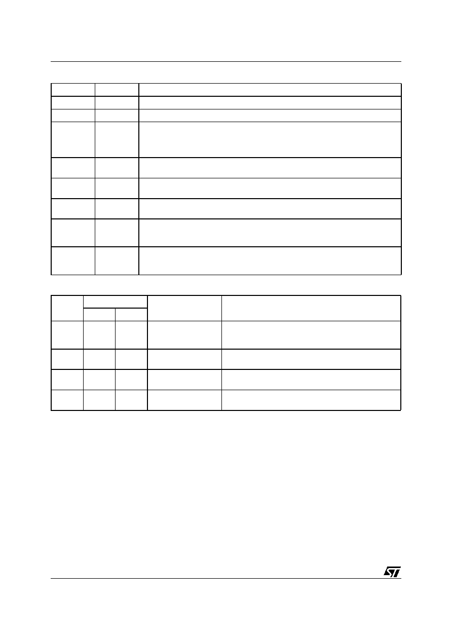
uPSD33XX
48/129
Table 42. SCON0 and SCON1 Register Details
Table 43. UART Operating Table
Bit Symbol
Function
7
SM0
See Table 43.
6
SM1
5
SM2
Enables the multiprocessor communication features in Mode 2 and 3. In Mode 2 or 3, if
SM2 is set to '1,' RI will not be activated if its received 8th data bit (RB8) is '0.' In Mode
1, if SM2=1, RI will not be activated if a valid Stop Bit was not received. In Mode 0, SM2
should be '0.'
4
REN
Enables serial reception. Set with software to enable reception. Clear with software to
disable reception.
3
TB8
The 8th data bit that will be transmitted in Modes 2 and 3. Set or clear with software as
desired
2
RB8
In Modes 2 and 3, this bit contains the 8th data bit that was received. In Mode 1, if
SM2=0, RB8 is the Snap Bit that was received. In Mode 0, RB8 is not used.
1
TI
Transmit Interrupt flag. Set by hardware at the end of the 8th bit time in Mode 0, or at the
beginning of the Stop Bit in the other modes, in any serial transmission. Must be cleared
with software.
0
RI
Receive Interrupt flag. Set by hardware at the end of the 8th bit time in Mode 0, or
halfway through the Stop Bit in the other modes, in any serial reception (except for
SM2). Must be cleared with software.
Mode
SCON
Baud Rate
Description
SM0
SM1
0
0
0
f
OSC
/12
Serial data enters and exits through RxD. TxD outputs the
shift clock.
8-bit are transmitted/received (LSB first)
1
0
1
Timer 1/2 overflow rate
8-bit UART
10 bits are transmitted (through TxD) or received (RxD).
2
1
0
f
OSC
/32 or f
OSC
/64
9-bit UART
11 bits are transmitted (through TxD) or received (RxD)
3
1
1
Timer 1/2 overflow rate
9-bit UART
Like Mode 2, except the variable baud rate.

49/129
uPSD33XX
Baud Rates. The baud rate in Mode 0 is fixed:
Mode 0 Baud Rate = f
OSC
/ 12
The baud rate in Mode 2 depends on the
value of Bit SMOD = 0 (which is the value on
reset), the baud rate is 1/64 the oscillator
frequency. If SMOD = 1, the baud rate is 1/32
the oscillator frequency.
Mode 2 Baud Rate = (2
SMOD
/ 64) x f
OSC
In the uPSD33XX Devices, the baud rates in
Modes 1 and 3 are determined by the Timer
1 overflow rate.
Using Timer 1 to Generate Baud Rates. When
Timer 1 is used as the baud rate generator, the
baud rates in Modes 1 and 3 are determined by
the Timer 1 overflow rate and the value of SMOD
as follows:
Mode 1,3 Baud Rate =
(2
SMOD
/ 32) x (Timer 1 overflow rate)
The Timer 1 Interrupt should be disabled in this
application. The Timer itself can be configured for
either "timer" or "counter" operation, and in any of
its 3 running modes. In the most typical applica-
tions, it is configured for "timer" operation, in the
Auto-reload Mode (high nibble of TMOD = 0010B).
In that case the baud rate is given by the formula:
Mode 1,3 Baud Rate =
(2
SMOD
/ 32) x (f
OSC
/ (12 x [256 ≠ (TH1)]))
One can achieve very low baud rates with Timer 1
by leaving the Timer 1 Interrupt enabled, and con-
figuring the Timer to run as a 16-bit timer (high nib-
ble of TMOD = 0001B), and using the Timer 1
Interrupt to do a 16-bit software reload. Figure 16,
page 41 lists various commonly used baud rates
and how they can be obtained from Timer 1.
Using Timer/Counter 2 to Generate Baud
Rates. In the uPSD33XX Devices, Timer 2 select-
ed as the baud rate generator by setting TCLK
and/or RCLK (see Figure 16, page 41, Timer/
Counter 2 Control Register).
Note: The baud rate for transmit and receive can
be simultaneously different. Setting RCLK and/or
TCLK puts Timer into its Baud Rate Generator
Mode.
The RCLK and TCLK Bits in the T2CON register
configure UART0. The RCLK1 and TCLK1 Bits in
the PCON register configure UART1.
The Baud Rate Generator Mode is similar to the
Auto-reload Mode, in that a roll over in TH2 causes
the Timer 2 registers to be reloaded with the 16-bit
value in registers RCAP2H and RCAP2L, which
are preset with software.
Now, the baud rates in Modes 1 and 3 are deter-
mined at Timer 2's overflow rate as follows:
Mode 1,3 Baud Rate =
Timer 2 Overflow Rate / 16
The timer can be configured for either "timer" or
"counter" operation. In the most typical applica-
tions, it is configured for "timer" operation (C/T2 =
0). "Timer" operation is a little different for Timer 2
when it's being used as a baud rate generator. In
this case, the baud rate is given by the formula:
Mode 1,3 Baud Rate =
f
OSC
/(32 x [65536 ≠ (RCAP2H, RCAP2L)]
where (RCAP2H, RCAP2L) is the content of
RC2H and RC2L taken as a 16-bit unsigned inte-
ger.
Timer 2 also may be used as the Baud Rate Gen-
erating Mode. This mode is valid only if RCLK +
TCLK = 1 in T2CON or in PCON.
Note: A roll-over in TH2 does not set TF2, and will
not generate an interrupt. Therefore, the Timer In-
terrupt does not have to be disabled when Timer 2
is in the Baud Rate Generator Mode.
Note: If EXEN2 is set, a 1-to-0 transition in T2EX
will set EXF2 but will not cause a reload from
(RCAP2H, RCAP2L) to (TH2, TL2). Thus when
Timer 2 is in use as a baud rate generator, T2EX
can be used as an extra external interrupt, if de-
sired.
Note: When Timer 2 is running (TR2 = 1) in "timer"
function in the Baud Rate Generator Mode, one
should not try to READ or WRITE TH2 or TL2. Un-
der these conditions the timer is being increment-
ed every state time, and the results of a READ or
WRITE may not be accurate.
The RC registers may be read, but should not be
written to, because a WRITE might overlap a re-
load and cause WRITE and/or reload errors.
Turn the timer off (clear TR2) before accessing the
Timer 2 or RC registers, in this case.

uPSD33XX
50/129
IRDA INTERFACE TO INFRARED TRANSCEIVER
The uPSD33XX provides an IrDA interface that
meets the IrDA Specification. The IrDA Interface
logic "pulse shaping" the UART1 (2nd UART) seri-
al signal from a UART Frame to an IrDA standard
IR Frame (and vise versa) that can be accepted by
a standard IrDA Transceiver. When enabled and
in transmitting mode, the IrDA Interface shortens
the UART output signal to IrDA compatible electri-
cal pulses. In receiving mode, the Interface
stretches the IrDA transceiver signal to the proper
bit rate to be received by the UART. The outputs
of the IrDA Interface drive the IrDA Transceiver di-
rectly.
The UART1 can operate in 4 modes, Mode 0 to
Mode 3. The IrDA Interface supports Mode 1 (10
bits transmit - Start Bit, 8 data bits and 1 Stop Bit)
only so as to be compatible with the IrDA format.
The IrDA Interface supports baud rate generated
by Timer 1 or Timer 2, but the Tx and Rx must be
of the same baud rate.
The features of the IrDA Interface are:
s
Stretches the UART pulse to 1.627µs; it
supports IrDA pulse from 1.41µs (Min) to 2,23µs
(Max) pulse or 3/16 bit pulse duration.
s
Support for baud rates from 1.2kHz to 115.2kHz
s
Direct interface to SIR transceiver from UART1
I/O pins (RxD1, TxD1) on Ports 1 or 4
s
IRDACON Register bits select pulse duration
and specify baud rate
The IrDA Interface is disabled on power-up and is
enabled by the IRDAEN Bit in the IRDACON Reg-
ister (see Table 44 and Table 45, page 50). When
it is disabled, the UART1's RxD and TxD bypass
the IrDA Interface and are connected directly to
the port pins. The IrDA Interface generates a
1.627µs or 3/16 bit pulse width output when the bit
is a '0' on the TxD line and stays '0' when the bit is
a '1.'
Figure 21. uPSD33XX IrDA Interface
Table 44. IRDACON Register Bit Definition (CEH, Reset Value 0FH)
Table 45. IRDACON Register Details
Bit 7
Bit 6
Bit 5
Bit 4
Bit 3
Bit 2
Bit 1
Bit 0
≠
IRDAEN
PULSE
CDIV4
CDIV3
CDIV2
CDIV1
CDIV0
BIT
SYMBOL
RW
Definition
7
≠
Reserved
6
IRDAEN
RW
IrDA Enable
0 = IrDA Interface is disabled
1 = IrDA is enabled, UART1 outputs are disconnected from Port 1
(or port 4)
UART1
IrDA
Interface
TxD
RxD
uPSD33XX
IrDA
Transceiver
TxD1-IrDA
RxD1-IrDA
SIRClk
AI07851

51/129
uPSD33XX
Baud Rate Select
There will be two schemes for IrDA pulse modula-
tion:
1. In the event of 3/16 bit time pulse modulation:
At maximum baud rate of 115.2kHz, the 3/16 bit
time pulse is 1.627µs.
2. In case of 1.627µs pulse modulation:
To implement 1.627µs pulse modulation, a
prescaler is needed to generate a subrefernce
clock (i.e, SIRClk) that is used to generate
1.627µs pulse modulation. Even though the
pulse width is 1.627µs, the baud rate follows the
configuration of UART1. Select a clock divider
to generate a F
SIRCLK
clock close to
1.8432MHz.
F
SIRCLK
= f
OSC
/ (CDIV[4:0])
where CDIV[4:0] must be 4 or larger.
Table 46. f
SIRCLK
Frequency
Note: 1. f
SIRCLK
at 1.8342MHz is needed to generate the 1.627µs pulse.
5
PULSE
RW
IrDA Pulse Modulation Select
0 = 1.627µs
1 = 3/16 bit time pulses
4-0
CDIV[4:0]
RW
Specify Clock Divider (see Table 46)
BIT
SYMBOL
RW
Definition
f
OSC
CDIV[4:0] (Clock divider)
f
SIRCLK
(1)
40.0MHz
22
1.8181MHz
33.0MHz
18
1.8333MHz
30.0MHz
16
1.8750MHz
24.0MHz
13
1.8461MHz
16.0MHz
9
1.7777MHz
12.0MHz
7
1.7142MHz

uPSD33XX
52/129
I
2
C INTERFACE
There is a serial I
2
C port implemented in the
uPSD33XX Devices. The serial port supports the
twin line I
2
C -bus and consists of a data line (SDA)
and a clock line (SCL). Depending on the configu-
ration, the SDA and SCL lines may require pull-up
resistors.
The system is unique because data transport,
clock generation, address recognition, and bus
control arbitration are all controlled by hardware.
The I
2
C serial I/O has complete autonomy in byte
handling and operates in 4 modes:
s
Master transmitter
s
Master receiver
s
Slave transmitter
s
Slave receiver
These functions are controlled by the I
2
C SFRs:
S1CON: the Control register - control of byte han-
dling and the operation of 4 mode
S1STA: the Status register - contents of its register
may also be used as a vector to various service
routines.
S1DAT: Data Shift register.
S1ADR: Slave Address register. Slave address
recognition is performed by On-Chip Hardware.
Table 49, page 53 shows the divisor values and
the I
2
C bit rate for some common f
OSC
frequen-
cies.
Figure 22. I
2
C Bus Block Diagram
I
2
C Registers Definition
Table 47. Serial Control Register S1CON (DCH, Reset Value 00H)
Slave Address
Shift Register
Arbitration + Sync. Logic
Bus Clock Generation
Control Register
Status Register
In
tern
al Bu
s
SDA
SCL
7
0
0
0
0
7
7
7
AI07852
Bit 7
Bit 6
Bit 5
Bit 4
Bit 3
Bit 2
Bit 1
Bit 0
CR2
ENI1
STA
STO
ADDR
AA
CR1
CR0

53/129
uPSD33XX
Table 48. S1CON Register Details
Table 49. Selection of the Serial Clock Frequency SCL in Master Mode
Note: 1. These values are beyond the supported bit rate.
Bit
Symbol
Function
7
CR2
This bit, along with Bits CR1and CR0 determines the serial clock frequency when SIO is
in the Master Mode.
6
ENI1
Enable IIC. When ENI1 = 0, the IIC is disabled. SDA and SCL outputs are in the high
impedance state.
5
STA
START flag. When this bit is set, the SIO H/W checks the status of the I
2
C bus and
generates a START condition if the bus is free. If the bus is busy, the SIO will generate a
repeated START condition when this bit is set.
When a START condition is detected on the I
2
C Bus, the I
2
C hardware clears the STA
flag.
Note: If this bit is set during an interrupt service, the START condition occurs after the
interrupt service.
4
STO
STOP flag. With this bit set while in Master Mode a STOP condition is generated.
When a STOP condition is detected on the I
2
C bus, the I
2
C hardware clears the STO
flag.
Note: If this bit is set during an interrupt service, the STOP condition occurs after the
interrupt service.
3
ADDR
This bit is set when address byte was received. Must be cleared with software.
2
AA
Acknowledge enable signal. If this bit is set, an acknowledge (low level to SDA is
returned during the acknowledge clock pulse on the SCL line when:
s
Own slave address is received;
s
A data byte is received while the device is programmed to be a Master Receiver;
s
A data byte is received while the device is a selected Slave Receiver; and
s
When this bit is reset, no acknowledge is returned.
SIO release SDA line as high during the acknowledge clock pulse.
1, 0
CR1, CR0
These two bits, along with the CR2 Bit determine the serial clock frequency when SIO is
in the Master Mode.
CR2
CR1
CR0
f
OSC
Divisor
Bit Rate (kHz) @ f
OSC
12MHz
24MHz
36MHz
40MHz
0
0
0
16
375
750
X
(1)
X
(1)
0
0
1
24
250
500
750
833
0
1
0
30
200
400
600
666
0
1
1
60
100
200
300
333
1
0
0
120
50
100
150
166
1
0
1
240
25
50
75
83
1
1
0
480
12.5
25
37.5
41
1
1
1
960
6.25
12.5
18.75
20
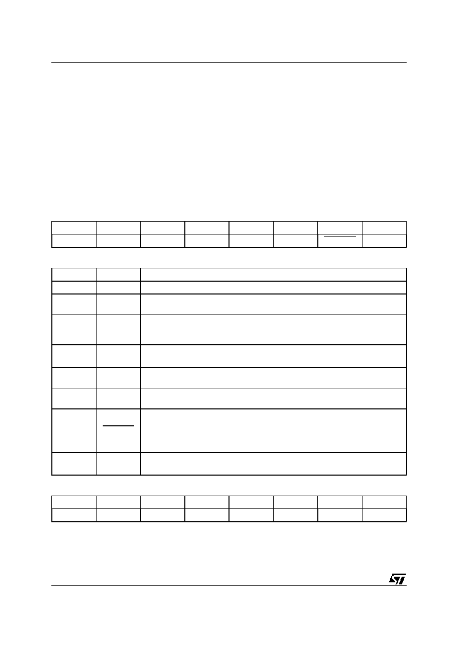
uPSD33XX
54/129
Serial Status Register (S1STA)
S1STA is a "Read only" register (except Bit 5 IN-
TR, see Table 50). The contents of this register
may be used as a vector to a service routine. This
optimized the response time of the software and
consequently that of the I
2
C bus.
The status codes for all possible modes of the I
2
C
bus interface are given Table 51.
This flag is set, and an interrupt is generated after
any of the following events occur.
1. Own slave address has been received during
AA = 1: ack_int
2. The general call address has been received
while GC(S1ADR.0) = 1 and AA = 1
3. A data byte has been received or transmitted in
Master Mode (even if arbitration is lost): ack_int
4. A data byte has been received or transmitted as
selected slave: ack_int
5. A Stop condition is received as selected slave
receiver or transmitter: stop_int
Data Shift Register (S1DAT)
S1DAT contains the serial data to be transmitted
or data which has just been received (see Table
52). The MSB (Bit 7) is transmitted or received
first; that is, data shifted from right to left.
Table 50. Serial Status Register S1STA (DDH, Reset Value 00H)
Table 51. S1STA Status Register Details
Table 52. Data Shift Register S1DAT (DEH, Reset Value 00H)
Bit 7
Bit 6
Bit 5
Bit 4
Bit 3
Bit 2
Bit 1
Bit 0
GC
STOP
INTR
TX_MODE
BBUSY
BLOST
ACK_REP
SLV
Bit
Symbol
Function
7
GC
General Call flag
6
STOP
STOP flag.
This bit is set when a STOP condition is received.
5
INTR
Interrupt flag.
This bit is set when a I
2
C interrupt is requested.
Must be cleared with software.
4
TX_MODE
Transmission Mode flag.
This bit is set when the I
2
C is a transmitter. Otherwise, this bit is reset.
3
BBUSY
Bus Busy State flag.
This bit is set when the bus is being used by another master. Otherwise, this bit is reset.
2
BLOST
Bus Lost flag.
This bit is set when the master loses the bus contention. Otherwise, this bit is reset.
1
ACK_REP
Acknowledge response flag.
This bit is set when the receiver transmits the not acknowledge signal.
This bit is reset when the receiver transmits the acknowledge signal.
Even if this bit is set, the STOP condition does not occur in the bus.
(MASTER MODE)
0
SLV
Slave Mode flag.
This bit is set when the I
2
C plays role in the slave mode. Otherwise, this bit is reset.
Bit 7
Bit 6
Bit 5
Bit 4
Bit 3
Bit 2
Bit 1
Bit 0
S1DAT7
S1DAT6
S1DAT5
S1DAT4
S1DAT3
S1DAT2
S1DAT1
S1DAT0
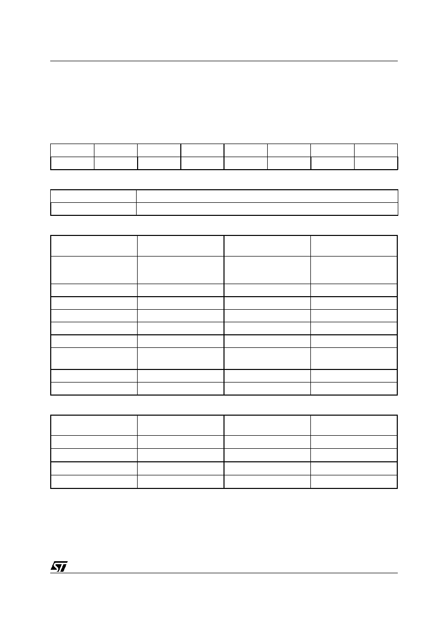
55/129
uPSD33XX
Address Register (S1ADR)
This 8-bit register may be loaded with the 7-bit
slave address to which the controller will respond
when programmed as a slave receive/transmitter
(see Table 53). The Start/Stop Hold Time Detec-
tion and System Clock registers (Table 54 and Ta-
ble 55) are included in the I
2
C unit to specify the
start/stop detection time to work with the large
range of MCU frequency values supported. Table
56 is an example with a system clock of 40MHz.
Table 53. Address Register S1ADR (DFH, Reset Value 00H)
Table 54. Start/Stop Hold Time Detection Register S1SETUP (DBH, Reset Value 00H)
Table 55. System Clock of 40MHz
Table 56. System Clock Setup Examples
Bit 7
Bit 6
Bit 5
Bit 4
Bit 3
Bit 2
Bit 1
Bit 0
SLA6
SLA5
SLA4
SLA3
SLA2
SLA1
SLA0
≠
Bit 7
Bit 6 - Bit 0
Enable S1SETU
Bit 6 - 0 specify the number of sample clocks
S1SETUP Register Value
No. of Sample Clock
(f
OSC
= 25ns)
Required Start/Stop
Hold Time
Note
00H
1EA
25ns
When Bit 7 (Enable bit) = 0,
the number of sample clock
is 1EA (ignore Bit 6 - Bit 0)
80h
1EA
25ns
81h
2EA
50ns
82h
3EA
75ns
...
...
8Bh
12EA
300ns
97h
24EA
600ns
Fast Mode I
2
C Start/Stop
Hold time specification
...
...
FFh
128EA
3000ns
System Clock
S1SETUP Register Value
No. of Sample Clock
Required Start/Stop
Hold Time
40MHz (f
OSC
-> 25ns)
97h
24EA
600ns
30MHz (f
OSC
-> 33.3ns)
91h
18EA
599ns
20MHz (f
OSC
-> 50ns)
8Bh
12EA
600ns
8MHz (f
OSC
-> 125ns)
84h
5EA
625ns

uPSD33XX
56/129
SPI (SYNCHRONOUS PERIPHERAL INTERFACE)
The SPI is a master interface that enables syn-
chronous, serial communication with external
slave peripherals. The SPI features full-duplex,
three-wire synchronous transfers and programma-
ble clock polarity (optional 4 wires). The SPI per-
forms parallel-to-serial conversion on data written
to a 8-bit wide Transmit data register (SPITDR)
and serial-to-parallel conversion on received data,
buffering a 8-bit wide Receive data register (SPIR-
DR).
The SPI supports a subset of the SPI function,
mainly the Master Mode with CPHA=1 Transfer
Format. It will be able to interface a device that has
a SPI Slave interface with the slave select being
grounded or controlled by the SPI. The CPHA=1
Transfer Format requires that the first data bit is
shifted out at the same time as the first SPICLK.
The SPI has the following features:
1. Support Master Mode, 8 bit data size
2. Programmable Clock Polarity
3. 8-bit wide, double-buffered transmit and receive
operation
4. Full-duplex - Both transmit and receive operate
simultaneously with two wires
5. 3, or 4 wires external pins (see Figure 23):
SPITxD ≠ This pin is used to transmit data out
of the SPI module.
SPIRxD ≠ This pin is used to receive data from
slave mode.
SPISEL ≠ This pin is used to output the select
signal from the SPI module to another
peripheral with which a data transfer is to take
place.
SPICLK ≠ This pin is used to output the SPICLK
clock
6. Programmable baud rate which can be
modulated by SPICLKD register
SPI Registers
The SPI has seven registers for data transmit, re-
ceive, and control (see Table 57, page 57 through
Table 61, page 58).
Figure 23. SPI Bus Interface
S P I
7
6
5
4
3
2
1
0
7
6
5
4
3
2
1
0
Tx_Shift_R eg
Rx_Shift_R eg
S PI TDR
S PI R D R
Clock Divider
f
OS C
Tx[7:0]
Rx[7:0]
S PI TXD
S PI R XD
S PI C LK
S PI S EL
S C LKDIV
AI07853

57/129
uPSD33XX
Table 57. SPI Registers
Table 58. SPICON0 (Control Register 0) Details (D6H, Reset Value 00H)
Register
SFR Offset
Dir.
Description
Reset Value
SPICON0
D6H
RW
Control Register 0
00
SPICON1
D7H
RW
Control Register 1
00
SPITDR
D4H
W
Transmit Data Register (data byte to be transmitted)
00
SPIRDR
D5H
R
Receive Data Register (store received data byte)
00
SPICLKD
D2H
RW
Clock Divider Value
04
SPISTAT
D3H
R
Status Register
02
BIT
SYMBOL
RW
Definition
7
≠
Reserved
6
TE
RW
Transmitter Enable
0 = Transmitter is disabled
1 = Transmitter is enabled
5
RE
RW
Receiver Enable
0 = Receiver is disabled
1 = Receiver is enabled
4
SPIEN
RW
SPI Enable
0 = SPI is disabled
1 = SPI is enabled
3
SSEL
RW
Slave Selection
0 = Slave Select output is disabled
1 = Slave Select output is enabled on Port pin P1.7 (or P4.7)
2
FLSB
RW
First LSB
0 = Transfer the most significant bit (MSB) first
1 = Transfer the least significant bit (LSB) first
1
SPO
RW
Sampling Polarity
0 = Sample transfer data at the falling edge of clock (SPICLK is '0'
when idle)
1 = Sample transfer data at the rising edge of clock (SPICLK is '1'
when idle)
0
≠
Reserved
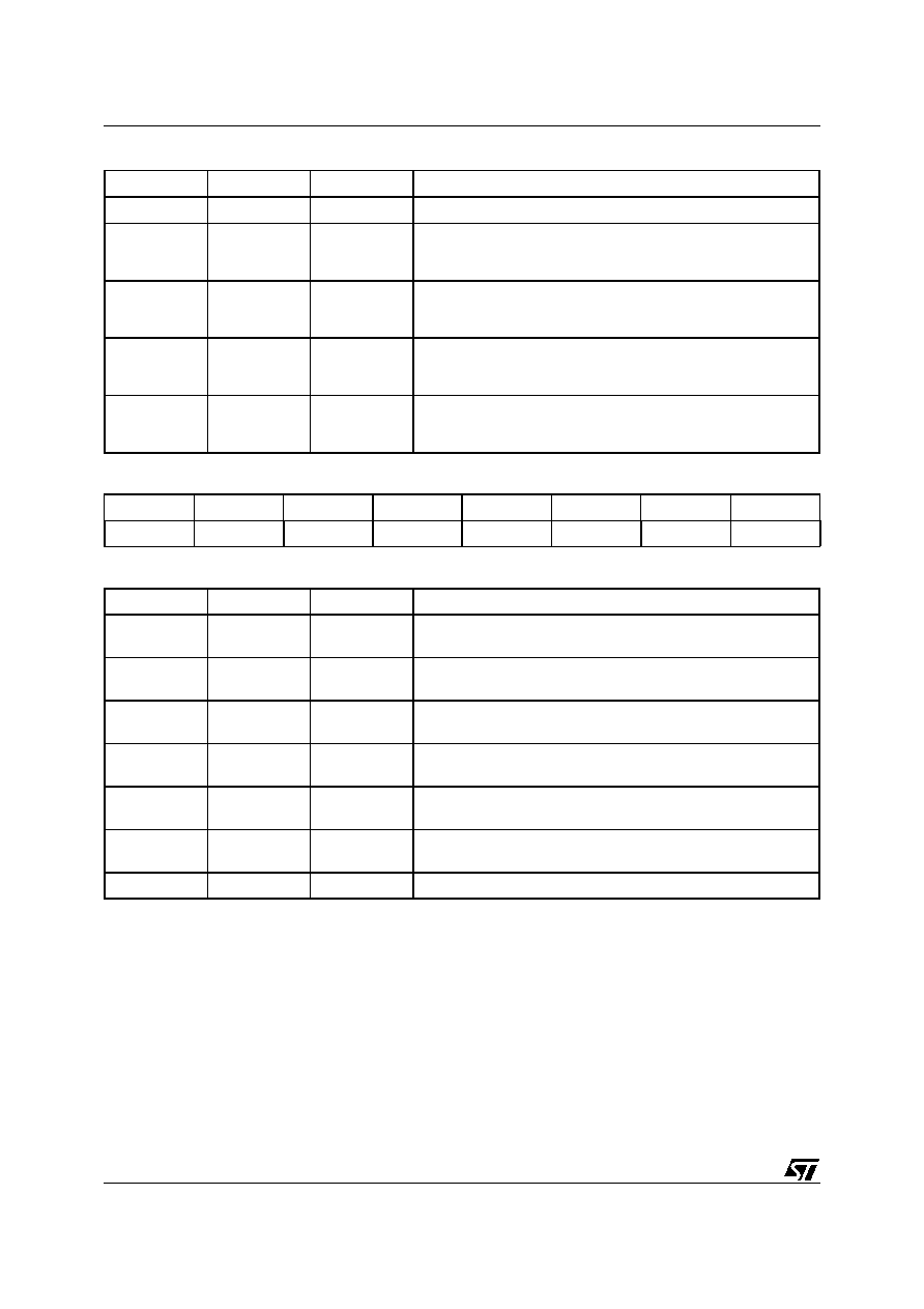
uPSD33XX
58/129
Table 59. SPICON1 (Control Register 1) Details (D7H, Reset Value 00H)
Table 60. SPICLKD (SPI Prescaler) Register (D2H, Reset Value 04H)
Table 61. SPICLKD (SPI Prescaler) Details
BIT
SYMBOL
RW
Definition
7-4
≠
Reserved
3
TEIE
RW
Transmission End Interrupt Enable
0 = SPI Transmission end Interrupt Disable
1 = SPI Transmission end Interrupt Enable
2
RORIE
RW
Receive Overrun Interrupt Enable
0 = Receive Overrun Interrupt Disable
1 = Receive Overrun Interrupt Enable
1
TIE
RW
Transmission Interrupt Enable
0 = SPITDR empty interrupt Disable
1 = SPITDR Empty interrupt Enable
0
RIE
RW
Reception Interrupt Enable
0 = SPIRDR full interrupt Disable
1 = SPIRDR full interrupt Enable
Bit 7
Bit 6
Bit 5
Bit 4
Bit 3
Bit 2
Bit 1
Bit 0
DIV128
DIV64
DIV32
DIV16
DIV8
DIV4
≠
≠
BIT
SYMBOL
RW
Definition
7
DIV128
RW
0 = No division
1 = Divide f
OSC
clock by 128
6
DIV64
RW
T0 = No division
1 = Divide f
OSC
clock by 64
5
DIV32
RW
0 = No division
1 = Divide f
OSC
clock by 32
4
DIV16
RW
0 = No division
1 = Divide f
OSC
clock by 16
3
DIV8
RW
0 = No division
1 = Divide f
OSC
clock by 8
2
DIV4
RW
0 = No division
1 = Divide f
OSC
clock by 4
1-0
Not Used
59/129
uPSD33XX
The SPI serial clock frequency in Master Mode is
the f
OSC
clock divided by the SPICLKD divisors.
The bits in the SPICLKD register can be set to pro-
vide divisor values of multiple of 4: 4, 8, 12, 16,
20... to 252.
Operation
The SPI transmitter and receiver share the same
clock but are independent, so full-duplex commu-
nication is possible. The transmitter and receiver
are also double-buffered, so continuous transmit-
ting or receiving (back-to-back transfer) is possible
by reading or writing data while transmitting or re-
ceiving is in progress.
SPI Configuration
The SPI is reset by the CPU Reset. Control regis-
ter SPICON0 needs to be programmed to decide
several operation parameters. The SPO Bit deter-
mines clock polarity. When SPO is set to '0,' the
data bit is placed on the communication line from
one rising edge of serial clock to the next and is
guaranteed valid at the fall of serial clock. When
SPO is set to '1,' the data bit is placed on the com-
munication line from one falling edge of serial
clock to the next and is guaranteed valid at the rise
of serial clock.
The FLSB Bit determines the format of 8-bit serial
data transfer. When FLSB is '0,' the 8-bit data is
transferred in order from MSB (first) to LSB (last).
When FLSB is '1,' the data is transferred in order
from LSB (first) to MSB (last).
The bit rate requires the programming of the clock
divider register SPICLKD. The value of SPICLKD
divides the f
OSC
clock to provide the serial transfer
clock output -SPICLK.
The SPICON1 and SPICON0 have SPI Transmit-
ter Enable (TE) and Receiver Enable (RE) and In-
terrupt Enable Bits (TEIE, RORIE,TIE, RIE). If TE
is disabled, both transmitting and receiving are
disabled because SPICLK is forced to LOW
(SPO=0) or HIGH (SPO=1).
Table 62. SPISTAT (Status) Register (D3H, Reset Value 02H)
Table 63. SPISTAT (Status) Register Details
Bit 7
Bit 6
Bit 5
Bit 4
Bit 3
Bit 2
Bit 1
Bit 0
≠
≠
≠
BUSY
TEISF
RORISF
TISF
RISF
BIT
SYMBOL
RW
Definition
7-5
Reserved
4
BUSY
R
SPI Busy
0 = Tx/Rx is completed
1 = Tx/Rx is on going
3
TEISF
R
Transmission End Interrupt Source flag
0 = Reset when users read this register
1 = Set when transmission end occurs
2
RORISF
R
Receive Overrun Interrupt Source flag
0 = Reset when user reads this register
1 = Set when Rx Overrun occurs
1
TISF
R
Transfer Interrupt Source flag
0 = Reset when SPITDR is full (when the SPITDR is written)
1 = Set when SPITDR is empty
0
RISF
R
Receive Interrupt Source flag
0 = Reset when SPIRDR is empty (when the SPITDR is read)
1 = Set when SPIRDR is full
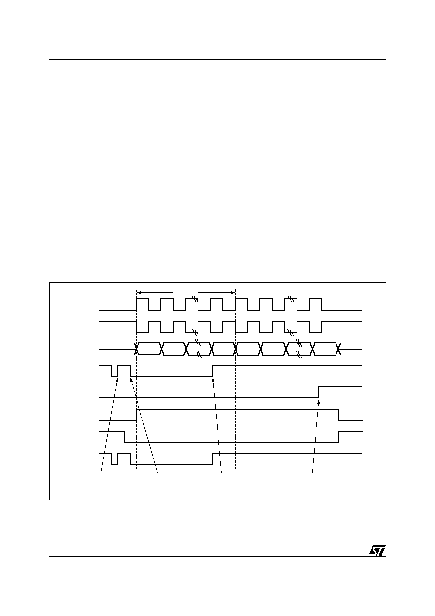
uPSD33XX
60/129
Slave Select Output
The SPI can be operated as a SPI bus in Master
Mode. The Slave Select (SPISEL) line in the SPI
bus is assigned to port pin P1.7 (or P4.7). When
the SSEL Bit is set in the Control Register, the SPI
drives the SPISEL line low to select the slave de-
vice before data transmission. The rising edge of
SPISEL occurs after the last bit is shifted out.
Transmit operation. In transmitting serial data,
the SPI operates as follows:
1. The initial sequence would be:
≠ CPU writes the byte to SPITDR,
≠ CPU sets SPIEN = 1, TIE = 1,
≠ CPU sets TE = 1 to enable transmit,
≠ SPI loads TSR with data from TDR, and
≠ SPI sets TISF and interrupts the CPU to write
the second byte.
2. In the ISR (Interrupt Service Routine) for SPI,
the CPU writes new data on SPITDR. This
update will automatically clear TISF.
3. If TISF is cleared (i.e., SPITDR has a valid data)
and the TSR (Transmit Shift Register) is ready
to load new data (e.g., the last bit (8th bit) of the
TSR is being sent, or the TSR is empty), the SPI
will load the TSR with data on SPITDR and set
TISF to '1' (i.e., request CPU to fill SPITDR).
4. The SPI checks the TISF flag when it outputs
the last bit (8th bit) of the eight-bit serial
transmission data.
≠ If the TISF flag is '0,' the SPI loads data from
SPITDR into the TSR and begins serial
transmission of the next 8-bit frame
(continuous transfer).
≠ If the TISF is '1,' the SPI sets the TEISF flag
to '1' in SPISTAT, and if the TEIE Bit is set to
'1' in SPICON1, a Transmit End Interrupt is
requested at this time.
So, the TISF Bit must be '0' before the last bit is
transmitted to perform continuous transfer. After
transmitting the last bit, the SPI holds the
SPITxD pin in the last bit state.
5. After the end of serial transmission, the SPICLK
pin is held in a constant state.
Figure 24. SPI Transmit Operation Example
Bit0
SPICLK
(SPO=0)
SPICLK
(SPO=1)
SPITXD
Bit1
Bit7
Bit0
Bit1
Bit7
1 frame
TISF
TEISF
BUSY
SPIINTR
SPITDR Empty
interrupt requested
Interrupt handler
write data in TDR
SPITDR Empty
interrupt requested
Transmit End
interrupt requested
SPISEL
AI07854

61/129
uPSD33XX
Receive Operation
In receiving serial data, the SPI operates as fol-
lows:
1. The SPI generates serial clock and
synchronizes internally.
2. Received data is stored in the RSR (Receive
Shift Register) in order from MSB to LSB
(FLSB = 0) or from LSB to MSB (FLSB = 1).
After receiving the data, the SPI checks to see if
the RIS flag is '0' or not.
If this check passes, the received data in the
RSR is stored in SPIRDR and the RIS flag is set
to 1.
When the check fails (i.e., the RIS flag is '1' or
the last received data in SPIRDR is not read
until the 8th bit of currently received data is
received in the RSR), the RORIS flag is set to '1'
and received data in the RSR is lost. When the
RORIS flag is set to '1' and the RORIE Bit is set
to '1' at SPICON1, the subsequent transmit and
receive operations are disabled.
3. If the RIE Bit in SPICON1 is set to '1' and the
RIS flag is set to '1,' the SPIRDR Full Interrupt is
requested.
If the RORIE Bit in SPICON1 is set to '1' and the
RORIS flag is set to '1,' the Receive Overrun
Interrupt is requested.
Figure 25. SPI Receive Operation Example
Bit7
SPICLK
(SPO=0)
SPICLK
(SPO=1)
SPIRXD
Bit0
Bit1
Bit7
Bit0
Bit1
Bit7
1 frame
RISF
RORIS
BUSY
SPIINTR
SPIRDR Full
interrupt requested
Interrupt handler
read data in SPIRDR
SPIRDR Full
interrupt requested
Transmit End
interrupt requested
AI07855

uPSD33XX
62/129
ANALOG-TO-DIGITAL CONVERTOR (ADC)
The ADC unit in the uPSD33XX is a SAR type
ADC with a SAR register, an auto-zero comparator
and three internal DACs. The unit has 8 input
channels with 10-bit resolution. The A/D converter
has its own V
REF
input (80-pin package only),
which specifies the voltage reference for the A/D
operations. The analog to digital converter (A/D)
allows conversion of an analog input to a corre-
sponding 10-bit digital value. The A/D module has
eight analog inputs (P1.0 through P1.7) to an 8x1
multiplexor. One ADC channel is selected by the
bits in the configuration register. The converter
generates a 10-bits result via successive approxi-
mation. The analog supply voltage is connected to
the V
REF
input, which powers the resistance lad-
der in the A/D module.
The A/D module has 3 registers, the control regis-
ter ACON, the A/D result register ADAT0, and the
second A/D result register ADAT1. The ADAT0
register stores Bits 0.. 7 of the converter output,
Bits 8.. 9 are stored in Bits 0..1 of the ADAT1 reg-
ister. The ACON register controls the operation of
the A/D converter module. Three of the bits in the
ACON register select the analog channel inputs,
and the remaining bits control the converter oper-
ation.
ADC channel pin input is enabled by setting the
corresponding bit in the P1SFS0 and P1SFS1 reg-
isters to '1' and the channel select bits in the
ACON register.
The ADC reference clock (ADCCLK) is generated
from f
OSC
divided by the divider in the ADCPS reg-
ister. The ADC operates within a range of 2 to
16MHz, with typical ADCCLK frequency at 8MHz.
The conversion time is 4µs typical at 8MHz.
The processing of conversion starts when the
Start Bit ADST is set to '1.' After one cycle, it is
cleared by hardware. The ADC is monotonic with
no missing codes. Measurement is by continuous
conversion of the analog input. The ADAT register
contains the results of the A/D conversion. When
conversion is complete, the result is loaded into
the ADAT. The A/D Conversion Status Bit ADSF is
set to '1.' The block diagram of the A/D module is
shown in Figure 26. The A/D status bit ADSF is set
automatically when A/D conversion is completed
and cleared when A/D conversion is in process.
In addition, the ADC unit sets the interrupt flag in
the ACON register after a conversion is complete
(if AINTEN is set to '1'). The ADC interrupts the
CPU when the enable bit AINTEN is set.
Port 1 ADC Channel Selects
The P1SFS0 and P1SFS1 Registers control the
selection of the Port 1 pin functions. When the
P1SFS0 Bit is '0,' the pin functions as a GPIO.
When bits are set to '1,' the pins are configured as
alternate functions. A new P1SFS1 Register se-
lects which of the alternate functions is enabled.
The ADC channel is enabled when the bit in
P1SFS1 is set to '1.'
Note: In the 52-pin package, there is no individual
V
REF
pin.
Figure 26. 10-Bit ADC
ANALOG
MUX
SELECT
ADC OUT - 10 BITS
ADAT 0 REG
ACON REG
CONTROL
10-BIT SAR ADC
ADAT1
REG
ADC0
ADC1
ADC2
ADC3
ADC4
ADC5
ADC6
ADC7
AVREF
P1.0
P1.1
P1.2
P1.3
P1.4
P1.5
P1.6
P1.7
AVREF
AI07856

63/129
uPSD33XX
Table 64. ACON Register (97H, Reset Value 00H)
Table 65. ACON Register Details
Table 66. ADCPS Register Details (94H, Reset Value 00H)
Table 67. ADAT0 Register (95H, Reset Value 00H)
Table 68. ADAT1 Register (96H, Reset Value 00H)
Bit 7
Bit 6
Bit 5
Bit 4
Bit 3
Bit 2
Bit 1
Bit 0
AINTF
AINTEN
ADEN
ADS2
ADS1
ADS0
ADST
ADSF
Bit
Symbol
Function
7
AINTF
ADC Interrupt flag. This bit must be cleared with software.
0 = No interrupt request
1 = The AINTF flag is set when ADSF goes from '0' to '1.' Interrupts CPU when both
AINTF and AINTEN are set to '1.'
6
AINTEN
ADC Interrupt Enable
0 = ADC interrupt is disabled
1 = ADC interrupt is enabled
5
ADEN
ADC Enable Bit
0 = ADC shut off and consumes no operating current
1 = Enable ADC. ADC must be enabled before setting the ADST Bit.
4.. 2
ADS2.. 0
Analog channel Select
000 Select channel 0 (P1.0)
001 Select channel 0 (P1.1)
010 Select channel 0 (P1.2)
011 Select channel 0 (P1.3)
101 Select channel 0 (P1.5)
110 Select channel 0 (P1.6)
111 Select channel 0 (P1.7)
1
ADST
ADC Start Bit
0 = Force to zero
1 = Start and ADC, then after one cycle, the bit is cleared to '0.'
0
ADSF
ADC Status Bit
0 = ADC conversion is not completed
1 = ADC conversion is completed. The bit can also be cleared with software.
Bit
Symbol
Function
7:4
≠
Reserved
3
ADCCE
ADC Conversion Reference Clock Enable
0 = ADC reference clock is disabled (default)
1 = ADC reference clock is enabled
2:0
ADCPS[2:0]
ADC Reference Clock PreScaler
f
ACLK
= f
OSC
/2
ADCPS[2:0]
Example: for f
OSC
= 40MHz and ADCPS[2:0] = 2, the f
ACLK
= 40/2
2
= 10MHz. f
ACLK
frequency range must be 2≠16MHz.
Bit
Symbol
Function
7:0
≠
Store ADC output, Bit 7 - 0
Bit
Symbol
Function
7:2
≠
Reserved
1.. 0
≠
Store ADC output, Bit 9, 8

uPSD33XX
64/129
PROGRAMMABLE COUNTER ARRAY (PCA) WITH PWM
There are two Programmable Counter Array
blocks (PCA0 and PCA1) in the uPSD33XX. A
PCA block consists of a 16-bit up-counter, which is
shared by three TCM (Timer Counter Module). A
TCM can be programmed to perform one of the
following four functions:
1. Capture Mode: capture counter values by
external input signals
2. Timer Mode
3. Toggle Output Mode
4. PWM Mode: fixed frequency (8-bit or 16-bit),
programmable frequency (8-bit only)
PCA Block
The 16-bit Up-Counter in the PCA block is a free-
running counter (except in PWM Mode with pro-
grammable frequency). The Counter has a choice
of clock input: from an external pin, Timer 0 Over-
flow, or PCA Clock.
A PCA block has 3 Timer Counter Modules (TCM)
which share the 16-bit Counter output. The TCM
can be configured to capture or compare counter
value, generate a toggling output, or PWM func-
tions. Except for the PWM function, the other TCM
functions can generate an interrupt when an event
occurs.
Every TCM is connected to a port pin in Port 4; the
TCM pin can be configured as an event input, a
PWMs, a Toggle Output, or as External Clock In-
put. The pins are general I/O pins when not as-
signed to the TCM.
The TCM operation is configured by Control regis-
ters and Capture/Compare registers. Table 69,
page 65 lists the SFR registers in the PCA blocks.
Figure 27. PCA0 Block Diagram
TIMER0
OVERFLOW
P4.3/ECI
PCACH0
8-bit
PCACL0
8-bit
CLKSEL1
IDLE MODE
(From CPU)
OVF0
INT
EOVFI
TCM0
TCM1
TCM2
PWM FREQ
COMPARE
P4.0/CEX0
P4.1/CEX1
P4.2/CEX2
16-bit up Timer/Counter
CLKSEL0
PCAIDLE
PCA0CLK
CLEAR COUNTER
EN_PCA
EN_ALL
AI07857

65/129
uPSD33XX
Table 69. PCA0 and PCA1 Registers
Operation of TCM Modes
Each of the TCM in a PCA block supports four
modes of operation. However, an exception is
when the TCM is configured in PWM Mode with
programmable frequency. In this mode, all TCM in
a PCA block must be configured in the same mode
or left to be not used.
Capture Mode
The CAPCOM registers in the TCM are loaded
with the counter values when an external pin input
changes state. The user can configure the counter
value to be loaded by positive edge, negative edge
or any transition of the input signal. At loading, the
TCM can generate an interrupt if it is enabled.
Timer Mode
The TCM modules can be configured as software
timers by enable the comparator. The user writes
a value to the CAPCOM registers, which is then
compared with the 16-bit counter. If there is a
match, an interrupt can be generated to CPU.
Toggle Mode
In this mode, the user writes a value to the TCM's
CAPCOM registers and enables the comparator.
When there is a match with the Counter output, the
output of the TCM pin toggles. This mode is a sim-
ple extension of the Timer Mode.
PWM Mode - (X8), Fixed Frequency
In this mode, one or all the TCM's can be config-
ured to have a fixed frequency PWM output on the
port pins. The PWM frequency depends on when
the low byte of the Counter overflows (module
256). The duty cycle of each TCM module can be
specified in the CAPCOMHn register. When the
PCA_Counter_L value is equal to or greater than
the value in CAPCOMHn, the PWM output is
switched to a high state. When the
PCA_Counter_L Register overflows, the content
in CAPCOMHn is loaded to CAPCOMLn and a
new PWM pulse starts.
SFR Address
Register Name
RW
Register Function
PCA0
PCA1
PCA0
PCA1
A2
PCACL0
PCACL1
RW
The low 8 bits of PCA 16-bit counter.
A3
PCACH0
PCACH1
RW
The high 8 bits of PCA 16-bit counter.
A4
PCACON0
PCACON1
RW
Control Register
s
Enable PCA, Timer Overflow flag , PCA
Idle Mode, and Select clock source.
A5
PCASTA
N/A
RW
Status Register, Interrupt Status flags
s
Common for both PCA Block 0 and 1.
A9,
AA,
AB
BD,
BE,
BF
TCMMODE0
TCMMODE1
TCMMODE2
TCMMODE3
TCMMODE4
TCMMODE5
RW
TCM Mode
s
Capture, Compare, and Toggle Enable
Interrupts
s
PWM Mode Select.
AC
AD
C1
C2
CAPCOML0
CAPCOMH0
CAPCOML3
CAPCOMH3
RW
Capture/Compare registers of TCM0
AF
B1
C3
C4
CAPCOML1
CAPCOMH1
CAPCOML4
CAPCOMH4
RW
Capture/Compare registers of TCM1
B2
B3
C5
C6
CAPCOML2
CAPCOMH2
CAPCOML5
CAPCOMH5
RW
Capture/Compare registers of TCM2
B4
C7
PWMF0
PWMF1
RW
The 8-bit register to program the PWM
frequency. This register is used for
programmable, 8-bit PWM Mode only.

uPSD33XX
66/129
Figure 28. Timer Mode
Note: m = 0: n = 0, 1, or 2
m = 1: n = 3, 4, or 5
Figure 29. PWM Mode - (X8), Fixed Frequency
Note: m = 0: n = 0, 1, or 2
m = 1: n = 3, 4, or 5
MATCH_TIMER
INTR
0
0
0
TCMMODEn
ENABLE
8
8
MATCH
PCASTA
CAPCOMLn
PCACLm
PCACHm
16-bit COMPARATOR
CAPCOMHn
INTFn
0
0
16-bit up Timer/Counter
8
8
EINTF
E_COMP CAP_PE
CAP_NE
MATCH
TOGGLE
PWM1
PWM0
RESET
WRITE to
CAPCOMHn
WRITE to
CAPCOMLn
1
0
EN_FLAG
D
C
AI07858
CAPCOMHn
OVERFLOW
ENABLE
8
PCACLm
8
CAPCOMLn
8-bit COMPARATORn
CEXn
MATCH
S
R
Q
Q
SET
CLR
0
0
TCMMODEn
0
0
0
EINTF
E_COMP CAP_PE
CAP_NE
MATCH
TOGGLE
PWM1
PWM0
AI07859

67/129
uPSD33XX
PWM Mode - (X8), Programmable Frequency
In this mode, the PWM frequency is not deter-
mined by the overflow of the low byte of the
Counter. Instead, the frequency is determined by
the PWMFm register. The user can load a value in
the PWMFm register, which is then compared to
the low byte of the Counter. If there is a match, the
Counter is cleared and the Load registers (PWM-
Fm, CAPCOMHn) are re-loaded for the next PWM
pulse. There is only one PWMFm Register which
serves all 3 TCM in a PCA block.
If one of the TCM modules is operating in this
mode, the other modules in the PCA must be con-
figured to the same mode or left not to be used.
The duty cycle of the PWM can be specified in the
CAPCOMHn register as in the PWM with fixed fre-
quency mode. Different TCM modules can have
their own duty cycle.
Note: The value in the Frequency register (PWM-
Fm) must be larger than the duty cycle register
(CAPCOM).
Figure 30. PWM Mode - (X8) Programmable Frequency
Note: m = 0: n = 0, 1, or 2
m = 1: n = 3, 4, or 5
CLR
PCACHm
PWM FREQ COMPARE
PWMFm = PCACLm
PCACLm
CAPCOMHn
CEXn
ENABLE
ENABLE
8
8
PWMFm
8-bit COMPARATORm
8-bit COMPARATORn
CAPCOMLn
MATCH
S
R
Q
Q
SET
CLR
8
0
0
TCMMODEn
0
0
0
EINTF
E_COMP CAP_PE
CAP_NE
MATCH
TOGGLE
PWM1
PWM0
AI07860
uPSD33XX
68/129
PWM Mode - Fixed Frequency, 16-bit
The operation of the 16-bit PWM is the same as
the 8-bit PWM with fixed frequency. In this mode,
one or all the TCM can be configured to have a
fixed frequency PWM output on the port pins. The
PWM frequency is depending on the clock input
frequency to the 16-bit Counter. The duty cycle of
each TCM module can be specified in the CAP-
COMHn and CAPCOMLn registers. When the 16
bit PCA_Counter is equal or greater than the val-
ues in registers CAPCOMHn and CAPCOMLn, the
PWM output is switched to a high state. When the
PCA_Counter overflows, CEXn is asserted low.
Writing to Capture/Compare Registers
When writing a 16-bit value to the PCA0 Capture/
Compare registers, the low byte should always be
written first. Writing to CAPCOMLn clears the
E_COMP bit to '0'; writing to CAPCOMHn sets
E_COMP to '1' the largest duty cycle is 100%
(CAPCOMHn CAPCOMLn = 0x0000), and the
smallest duty cycle is 0.0015% (CAPCOMHn
CAPCOMLn = 0xFFFF). A 0% duty cycle may be
generated by clearing the E_COMP bit to `0'.
Control Register Bit Definition
Each PCA has its own PCA_CONFIGn, and each
module within the PCA block has its own
TCM_Mode Register which defines the operation
of that module (see Table 70 through Table 72).
There is one PCA_STATUS Register that covers
both PCA0 and PCA1 (see Table 73, page 68 and
Table 74, page 69).
Table 70. PCA0 Control Register PCACON0 (0A4H, Reset Value 00H)
Table 71. PCA1 Control Register PCACON0 (0BCH, Reset Value 00H)
Table 72. PCA0, PCA1 Register Details
Table 73. PCA Status Register PCASTA (0A5H, Reset Value 00H)
Bit 7
Bit 6
Bit 5
Bit 4
Bit 3
Bit 2
Bit 1
Bit 0
EN-ALL
EN_PCA
EOVFI
PCAIDLE
≠
≠
CLK_SEL[1:0]
Bit 7
Bit 6
Bit 5
Bit 4
Bit 3
Bit 2
Bit 1
Bit 0
EN-ALL
EN_PCA
EOVFI
PCAIDLE
≠
≠
CLK_SEL[1:0]
Bit
Symbol
Function
7
EN-ALL
0 = No impact on TCM modules
1 = Enable both PCA counters simultaneously (override the EN_PCA Bits)
This bit is to synchronize the two 16-bit counters in the PCA. For customers who want 5
PWM, for example, this bit can synchronize all of the PWM outputs.
6
EN_PCA
0 = PCA counter is disabled
1 = PCA counter is enabled
EN_PCA Counter Run Control Bit. Set with software to turn the PCA counter on. Must
be cleared with software to turn the PCA counter off.
5
EOVFI
1 = Enable Counter Overflow Interrupt if overflow flag (OVF) is set
4
PCAIDLE
0 = PCA operates when CPU is in Idle Mode
1 = PCA stops running when CPU is in Idle Mode
3-2
≠
Reserved
1-0
CLK_SEL
[1:0]
00 Select Prescaler clock as Counter clock
01 Select Timer 0 Overflow
10 Select External Clock pin (P4.3 for PCA0, P4.7 for PCA1) (MAX clock rate = f
OSC
/4)
Bit 7
Bit 6
Bit 5
Bit 4
Bit 3
Bit 2
Bit 1
Bit 0
OVF1
INTF5
INTF4
INTF3
OVF0
INTF2
INTF1
INTF0
69/129
uPSD33XX
Table 74. PCA Status Register PCASTA Details
TCM Interrupts
There are 8 TCM interrupts: 6 match or capture in-
terrupts and two counter overflow interrupts. The 8
interrupts are "ORed" as one PCA interrupt to the
CPU. By the nature of PCA application, it is unlike-
ly that many of the interrupts occur simultaneous-
ly. If they do, the CPU has to read the interrupt
flags and determine which one to serve. The soft-
ware has to clear the interrupt flag in the Status
Register after serving the interrupt.
Table 75. TCMMODE0 - TCMMODE5 (6 Registers, Reset Value 00H)
Bit
Symbol
Function
7
OFV1
PCA1 Counter OverFlow flag.
Set by hardware when the counter rolls over. OVF1 flags an interrupt if Bit EOVFI in
PCACON1 is set. OVF1 may be set with either hardware or software but can only be
cleared with software.
6
INTF5
TCM5 Interrupt flag.
Set by hardware when a match or capture event occurs.
Must be clear with software.
5
INTF4
TCM4 Interrupt flag.
Set by hardware when a match or capture event occurs.
Must be clear with software.
4
INTF3
TCM3 Interrupt flag.
Set by hardware when a match or capture event occurs.
Must be clear with software.
3
OVF0
PCA0 Counter OverFlow flag.
Set by hardware when the counter rolls over. OVF0 flags an interrupt if Bit EOVFI in
PCACON0 is set. OVF1 may be set with either hardware or software but can only be
cleared with software.
2
INTF2
TCM2 Interrupt flag.
Set by hardware when a match or capture event occurs.
Must be clear with software.
1
INTF1
TCM1 Interrupt flag.
Set by hardware when a match or capture event occurs.
Must be clear with software.
0
INTF0
TCM0 Interrupt flag.
Set by hardware when a match or capture event occurs.
Must be clear with software.
Bit 7
Bit 6
Bit 5
Bit 4
Bit 3
Bit 2
Bit 1
Bit 0
EINTF
E_COMP
CAP_PE
CAP_NE
MATCH
TOGGLE
PWM[1:0]

uPSD33XX
70/129
Table 76. TCMMODE0 - TCMMODE5 Register Details
Table 77. TCMMODE Register Configurations
e
Symbol
Function
7
EINTF
1 - Enable the interrupt flags (INTF) in the Status Register to generate an interrupt.
6
E_COMP
1 - Enable the comparator when set
5
CAP_PE
1 - Enable Capture Mode, a positive edge on the CEXn pin.
4
CAP_NE
1 - Enable Capture Mode, a negative edge on the CEXn pin.
3
MATCH
1 - A match from the comparator sets the INTF bits in the Status Register.
2
TOGGLE
1 - A match on the comparator results in a toggling output on CEXn pin.
1-0
PWM[1:0]
01 Enable PWM Mode (x8), fixed frequency. Enable the CEXn pin as a PWM output.
10 Enable PWM Mode (x8) with programmable frequency. Enable the CEXn pin as a
PWM output.
11 Enable PWM Mode (x16), fixed frequency. Enable the CEXn pin as a PWM output.
EINTF
E_COMP
CAP_PE
CAP_NE
MATCH
TOGGLE
PWM1
PWM0
TCM FUNCTION
0
0
0
0
0
0
0
0
No operation (reset value)
0
1
0
0
0
0
0
1
8-bit PWM, fixed frequency
0
1
0
0
0
0
1
0
8-bit PWM, programmable
frequency
0
1
0
0
0
0
1
1
16-bit PWM, fixed frequency
X
1
0
0
1
1
0
0
16-bit toggle
X
1
0
0
1
0
0
0
16-bit Software Timer
X
X
0
1
0
0
0
0
16-bit capture, negative trigger
X
X
1
0
0
0
0
0
16-bit capture, positive trigger
X
X
1
1
0
0
0
0
16-bit capture, transition trigger

71/129
uPSD33XX
PSD MODULE
s
The PSD Module provides configurable
Program and Data memories to the Turbo 8032
MCU Module. In addition, it has its own set of I/
O ports and a PLD with 16 macrocells for
general logic implementation.
s
Ports A,B,C, and D are general purpose
programmable I/O ports that have a port
architecture which is different from the I/O ports
in the MCU Module.
s
The PSD Module communicates with the MCU
Module through the internal address, data bus
(A0-A15, D0-D7) and control signals (RD, WR,
PSEN, ALE, RESET). The user defines the
Decoding PLD in the PSDsoft Development
Tool and can map the resources in the PSD
Module to any program or data address space.
Figure 31, page 72 shows the functional blocks
in the PSD Module.
Functional Overview
s
64K, 128K, or 256K bytes Flash memory. This
is the main Flash memory. It is divided into
equally-sized blocks that can be accessed with
user-specified addresses.
s
Secondary 16K or 32K bytes Flash boot
memory. It is divided into equally-sized blocks
that can be accessed with user-specified
addresses. This secondary memory brings the
ability to execute code and update the main
Flash
concurrently.
s
2K, 8K, or 32K bytes SRAM. The SRAM's
contents can be protected from a power failure
by connecting an external battery.
s
CPLD with 16 Output Micro Cells (OMCs} and
20 Input Micro Cells (IMCs). The CPLD may be
used to efficiently implement a variety of logic
functions for internal and external control.
Examples include state machines, loadable
shift registers, and loadable counters.
s
Decode PLD (DPLD) that decodes address for
selection of memory blocks in the PSD Module.
s
Configurable I/O ports (Port A,B,C and D) that
can be used for the following functions:
≠ MCU I/Os
≠ PLD I/Os
≠ Latched MCU address output
≠ Special function I/Os.
≠ I/O ports may be configured as open-drain
outputs.
s
Built-in JTAG compliant serial port allows full-
chip In-System Programmability (ISP). With it,
you can program a blank device or reprogram a
device in the factory or the field.
s
Internal page register that can be used to
expand the 8032 MCU Module address space
by a factor of 256.
s
Internal programmable Power Management
Unit (PMU) that supports a low-power mode
called Power-down Mode. The PMU can
automatically detect a lack of the 8032 CPU
core activity and put the PSD Module into
Power-down Mode.
s
Erase/WRITE cycles:
≠ Flash memory - 100,000 minimum
≠ PLD - 1,000 minimum
≠ Data Retention: 15 year minimum (for Main
Flash memory, Boot, PLD and Configuration
bits)

uPSD33XX
72/129
Figure 31. PSD Module Block Diagram
BUS
Interface
WR_, RD_,
PSEN_, ALE,
RESET_,
A0-A15
D0 ≠ D7
CLKIN
(PD1)
CLKIN
CLKIN
PLD
INPUT
BUS
PROG.
PORT
PORT
A
PROG.
PORT
PORT
B
POWER
MANGMT
UNIT
PRIMARY
FLASH MEMORY
VSTDBY
PA0 ≠ PA7
PB0 ≠ PB7
PROG.
PORT
PORT
C
PROG.
PORT
PORT
D
PC0 ≠ PC7
PD1 ≠ PD2
ADDRESS
/
DATA
/
CONTROL BUS
PORT A ,B & C
2 EXT CS TO PORT D
20 INPUT MACROCELLS
PORT A ,B & C
73
73
SECONDARY
NON-VOLATILE MEMORY
(BOOT OR DATA)
BATTERY
BACKUP SRAM
RUNTIME CONTROL
AND I/O REGISTERS
SRAM SELECT
PERIP I/O MODE SELECTS
MACROCELL FEEDBACK OR PORT INPUT
CSIOP
FLASH ISP CPLD
(CPLD)
16 OUTPUT MACROCELLS
FLASH DECODE
PLD
( DPLD
)
PLD, CONFIGURATION
& FLASH MEMORY
LOADER
JTAG
SERIAL
CHANNEL
( PC2
)
PAGE
REGISTER
EMBEDDED
ALGORITHM
SECTOR
SELECTS
SECTOR
SELECTS
GLOBAL
CONFIG. &
SECURITY
AI07872
8
BUS
Interface
8032 Bus

73/129
uPSD33XX
PSD MODULE REGISTER DESCRIPTION AND ADDRESS OFFSET
Table 78 shows the offset addresses to the PSD
Module registers relative to the CSIOP base ad-
dress. The CSIOP space is the 256 bytes of ad-
dress that is allocated by the user to the internal
PSD Module registers. Table 80, page 75 provides
brief descriptions of the registers in CSIOP space.
The following section gives a more detailed de-
scription.
Table 78. Register Address Offset
Note: 1. Other registers that are not part of the I/O ports.
Register Name
Port A Port B
Port C
Port D Other
(1)
Description
Data In
00
01
10
11
Reads Port pin as input, MCU I/O Input Mode
Control
02
03
Selects mode between MCU I/O or Address Out
Data Out
04
05
12
13
Stores data for output to Port pins, MCU I/O
Output Mode
Direction
06
07
14
15
Configures Port pin as input or output
Drive Select
08
09
16
17
Configures Port pins as either CMOS or Open
Drain on some pins, while selecting high slew
rate on other pins.
Input Macrocell
0A
0B
18
Reads Input Macrocells
Enable Out
0C
0D
1A
1B
Reads the status of the output enable to the I/O
Port driver
Output Macrocells
AB
20 20
READ ≠ reads output of macrocells AB
WRITE ≠ loads macrocell flip-flops
Output Macrocells
BC
21 21
READ ≠ reads output of macrocells BC
WRITE ≠ loads macrocell flip-flops
Mask Macrocells AB
22
22
Blocks writing to the Output Macrocells AB
Mask Macrocells BC
23
23
Blocks writing to the Output Macrocells BC
Primary Flash
Protection
C0
Read-only ≠ Primary Flash Sector Protection
Secondary Flash
memory Protection
C2
Read-only ≠ PSD Module Security and
Secondary Flash memory Sector Protection
PMMR0
B0
Power Management Register 0
PMMR2
B4
Power Management Register 2
Page E0
Page
Register
VM E2
Places PSD Module memory areas in Program
and/or Data space on an individual basis.
uPSD33XX
74/129
PSD MODULE DETAILED OPERATION
As shown in Figure 31, page 72, the PSD Module
consists of five major types of functional blocks:
s
Memory Block
s
PLD Blocks
s
I/O Ports
s
Power Management Unit (PMU)
s
JTAG Interface
The functions of each block are described in the
following sections. Many of the blocks perform
multiple functions, and are user configurable.
MEMORY BLOCKS
The PSD Module has the following memory blocks
(see Table 79):
≠ Primary Flash memory
≠ Secondary Flash memory
≠ SRAM
The Memory Select signals for these blocks origi-
nate from the Decode PLD (DPLD) and are user-
defined in PSDsoft Express.
Primary Flash Memory and Secondary Flash
memory Description
The primary Flash memory is divided evenly into
eight equal sectors. The secondary Flash memory
is divided into four equal sectors. Each sector of
either memory block can be separately protected
from Program and Erase cycles.
Flash memory may be erased on a sector-by-sec-
tor basis. Flash sector erasure may be suspended
while data is read from other sectors of the block
and then resumed after reading.
During a Program or Erase cycle in Flash memory,
the status can be output on Ready/Busy (PC3).
This pin is set up using PSDsoft Express Configu-
ration.
Memory Block Select Signals
The DPLD generates the Select signals for all the
internal memory blocks (see the section entitled
"PLDs," page 84). Each of the sectors of the pri-
mary Flash memory has a Select signal (FS0-FS7)
which can contain up to three product terms. Each
of the four sectors of the secondary Flash memory
has a Select signal (CSBOOT0-CSBOOT3) which
can contain up to three product terms. Having
three product terms for each Select signal allows
a given sector to be mapped in Program or Data
space.
Flash Memory Instructions
The Flash memory instructions are detailed in Ta-
ble 80. For efficient decoding of the instructions,
the first two bytes of an instruction are the coded
cycles and are followed by an instruction byte or
confirmation byte. The coded cycles consist of
writing the data AAh to address X555h during the
first cycle and data 55h to address XAAAh during
the second cycle. Address signals A15-A12 are
Don't Care during the instruction WRITE cycles.
However, the appropriate Sector Select (FS0-FS7
or CSBOOT0-CSBOOT3) must be selected.
The primary and secondary Flash memories have
the same instruction set (except for Read Primary
Flash Identifier). The Sector Select signals deter-
mine which Flash memory is to receive and exe-
cute the instruction. The primary Flash memory is
selected if any one of Sector Select (FS0-FS7) is
High, and the secondary Flash memory is selected
if any one of Sector Select (CSBOOT0-
CSBOOT3) is High.
Table 79. uPSD33XX Memory Configuration
Device
Main Flash
Secondary Flash
SRAM
Flash Size
Sector Size
# of Sectors
(Sector Select
Signal)
Flash Size
Sector Size
# of Sectors
(Sector Select
Signal)
Size
uPSD3312
64KB
16KB
4 (FS0-3)
16KB
8KB
2 (CSBOOT0-1)
2KB
uPSD3333
128KB
16KB
8 (FS0-7)
32KB
8KB
4 (CSBOOT0-3)
8KB
uPSD3334
256KB
32KB
8 (FS0-7)
32KB
8KB
4 (CSBOOT0-3)
32KB
uPSD3354
256KB
32KB
8 (FS0-7)
32KB
8KB
4 (CSBOOT0-3)
32KB

75/129
uPSD33XX
Table 80. Instructions
Note: 1. All bus cycles are WRITE bus cycles, except the ones with the "Read" label
2. All values are in hexadecimal:
X = Don't care. Addresses of the form XXXXh, in this table, must be even addresses
RA = Address of the memory location to be read
RD = Data READ from location RA during the READ cycle
PA = Address of the memory location to be programmed. Addresses are latched on the falling edge of WRITE Strobe (WR, CNTL0).
PA is an even address for PSD in Word Programming Mode.
PD = Data word to be programmed at location PA. Data is latched on the rising edge of WRITE Strobe (WR , CNTL0)
SA = Address of the sector to be erased or verified. The Sector Select (FS0-FS7 or CSBOOT0-CSBOOT3) of the sector to be
erased, or verified, must be Active (High).
3. Sector Select (FS0-FS7 or CSBOOT0-CSBOOT3) signals are active High, and are defined in PSDsoft Express.
4. Only address Bits A11-A0 are used in instruction decoding.
5. No Unlock or instruction cycles are required when the device is in the READ Mode
6. The RESET instruction is required to return to the READ Mode after reading the Sector Protection Status, or if the Error Flag Bit
(DQ5/DQ13) goes High.
7. Additional sectors to be erased must be written at the end of the Sector Erase instruction within 80µs.
8. The data is 00h for an unprotected sector, and 01h for a protected sector. In the fourth cycle, the Sector Select is active, and
(A1,A0)=(1,0)
9. The Unlock Bypass instruction is required prior to the Unlock Bypass Program instruction.
10. The Unlock Bypass Reset Flash instruction is required to return to reading memory data when the device is in the Unlock Bypass
Mode.
11. The system may perform READ and Program cycles in non-erasing sectors, read the Flash ID or read the Sector Protection Status
when in the Suspend Sector Erase Mode. The Suspend Sector Erase instruction is valid only during a Sector Erase cycle.
12. The Resume Sector Erase instruction is valid only during the Suspend Sector Erase Mode.
13. The MCU cannot invoke these instructions while executing code from the same Flash memory as that for which the instruction is
intended. The MCU must retrieve, for example, the code from the secondary Flash memory when reading the Sector Protection
Status of the primary Flash memory.
Instruction
FS0-FS7 or
CSBOOT0-
CSBOOT3
Cycle 1
Cycle 2
Cycle 3
Cycle 4
Cycle 5
Cycle 6
Cycle 7
READ
(5)
1
"Read"
RD @ RA
READ Sector
Protection
(6,8,13)
1
AAh@
X555h
55h@
XAAAh
90h@
X555h
Read status @
XX02h
Program a Flash
Byte
(13)
1
AAh@
X555h
55h@
XAAAh
A0h@
X555h
PD@ PA
Flash Sector
Erase
(7,13)
1
AAh@
X555h
55h@
XAAAh
80h@
X555h
AAh@ X555h
55h@
XAAAh
30h@
SA
30h
7
@
next SA
Flash Bulk
Erase
(13)
1
AAh@
X555h
55h@
XAAAh
80h@
X555h
AAh@ X555h
55h@
XAAAh
10h@
X555h
Suspend Sector
Erase
(11)
1
B0h@
XXXXh
Resume Sector
Erase
(12)
1
30h@
XXXXh
RESET
(6)
1
F0h@
XXXXh
Unlock Bypass
1
AAh@
X555h
55h@
XAAAh
20h@
X555h
Unlock Bypass
Program
(9)
1
A0h@
XXXXh
PD@ PA
Unlock Bypass
Reset
(10)
1
90h@
XXXXh
00h@
XXXXh

uPSD33XX
76/129
READ Flash Memory
After power-up, the MCU may read the primary
Flash memory or the secondary Flash memory us-
ing READ operations just as it would a ROM or
RAM device. Alternately, the MCU may use READ
operations to obtain status information about a
Program or Erase cycle that is currently in
progress. Lastly, the MCU may use instructions to
read sector protection and the Erase/Program sta-
tus bits.
Reading the Erase/Program Status Bits. The
Flash memory provides several status bits to be
used by the MCU to confirm the completion of an
Erase or Program cycle of Flash memory. These
status bits minimize the time that the MCU spends
performing these tasks and are defined in Table
81, page 77. The status bits can be read as many
times as needed.
For Flash memory, the MCU can perform a READ
operation to obtain these status bits while an
Erase or Program instruction is being executed by
the embedded algorithm. See the section entitled
"Programming Flash Memory, page 77," for de-
tails.
Data Polling Flag (DQ7). When erasing or pro-
gramming in Flash memory, the Data Polling Flag
Bit (DQ7) outputs the complement of the bit being
entered for programming/writing on the DQ7 Bit.
Once the Program instruction or the WRITE oper-
ation is completed, the true logic value is read on
the Data Polling Flag Bit (DQ7) (in a READ opera-
tion).
s
Data Polling is effective after the fourth WRITE
pulse (for a Program instruction) or after the
sixth WRITE pulse (for an Erase instruction). It
must be performed at the address being
programmed or at an address within the Flash
memory sector being erased.
s
During an Erase cycle, the Data Polling Flag Bit
(DQ7) outputs a '0.' After completion of the
cycle, the Data Polling Flag Bit (DQ7) outputs
the last bit programmed (it is a '1' after erasing).
s
If the byte to be programmed is in a protected
Flash memory sector, the instruction is ignored.
s
If all the Flash memory sectors to be erased are
protected, the Data Polling Flag Bit (DQ7) is
reset to '0' for about 100µs, and then returns to
the previous addressed byte. No erasure is
performed.
Toggle Flag (DQ6). The Flash memory offers an-
other way for determining when the Program cycle
is completed. During the internal WRITE operation
and when either the FS0-FS7 or CSBOOT0-
CSBOOT3 is true, the Toggle Flag Bit (DQ6) tog-
gles from '0' to '1' and '1' to '0' on subsequent at-
tempts to read any byte of the memory.
When the internal cycle is complete, the toggling
stops and the data READ on the Data Bus D0-D7
is the addressed memory byte. The device is now
accessible for a new READ or WRITE operation.
The cycle is finished when two successive Reads
yield the same output data.
s
The Toggle Flag Bit (DQ6) is effective after the
fourth WRITE pulse (for a Program instruction)
or after the sixth WRITE pulse (for an Erase
instruction).
s
If the byte to be programmed belongs to a
protected Flash memory sector, the instruction
is ignored.
s
If all the Flash memory sectors selected for
erasure are protected, the Toggle Flag Bit
(DQ6) toggles to '0' for about 100µs and then
returns to the previous addressed byte.
Error Flag (DQ5). During a normal Program or
Erase cycle, the Error Flag Bit (DQ5) is to '0.' This
bit is set to '1' when there is a failure during Flash
memory Byte Program, Sector Erase, or Bulk
Erase cycle.
In the case of Flash memory programming, the Er-
ror Flag Bit (DQ5) indicates the attempt to program
a Flash memory bit from the programmed state,
'0', to the erased state, '1,' which is not valid. The
Error Flag Bit (DQ5) may also indicate a Time-out
condition while attempting to program a byte.
In case of an error in a Flash memory Sector Erase
or Byte Program cycle, the Flash memory sector in
which the error occurred or to which the pro-
grammed byte belongs must no longer be used.
Other Flash memory sectors may still be used.
The Error Flag Bit (DQ5) is reset after a Reset
Flash instruction.
Erase Time-out Flag (DQ3). The Erase Time-
out Flag Bit (DQ3) reflects the time-out period al-
lowed between two consecutive Sector Erase in-
structions. The Erase Time-out Flag Bit (DQ3) is
reset to '0' after a Sector Erase cycle for a time pe-
riod of 100µs + 20% unless an additional Sector
Erase instruction is decoded. After this time peri-
od, or when the additional Sector Erase instruction
is decoded, the Erase Time-out Flag Bit (DQ3) is
set to '1.'
77/129
uPSD33XX
Table 81. Status Bit
Note: 1. X = Not guaranteed value, can be read either '1' or '0.'
2. DQ7-DQ0 represent the Data Bus bits, D7-D0.
3. FS0-FS7 and CSBOOT0-CSBOOT3 are active High.
Programming Flash Memory
Flash memory must be erased prior to being pro-
grammed. A byte of Flash memory is erased to all
'1s' (FFh), and is programmed by setting selected
bits to '0.' The MCU may erase Flash memory all
at once or by-sector, but not byte-by-byte. Howev-
er, the MCU may program Flash memory byte-by-
byte.
The primary and secondary Flash memories re-
quire the MCU to send an instruction to program a
byte or to erase sectors (see Table 80, page 75).
Once the MCU issues a Flash memory Program or
Erase instruction, it must check for the status bits
for completion. The embedded algorithms that are
invoked support several means to provide status
to the MCU. Status may be checked using any of
three methods: Data Polling, Data Toggle, or
Ready/Busy (PC3).
Figure 32. Data Polling Flowchart
Figure 33. Data Toggle Flowchart
Functional Block
FS0-FS7/
CSBOOT0-
CSBOOT3
DQ7
(2)
DQ6
(2)
DQ5
(2)
DQ4
(1,2)
DQ3
(2)
DQ2
(1,2)
DQ1
(1,2)
DQ0
(1,2)
Flash Memory
V
IH
(3)
Data
Polling
Toggle
Flag
Error
Flag
X
Erase
Time-
out
X
X
X
READ DQ5 & DQ7
at VALID ADDRESS
START
READ DQ7
FAIL
PASS
AI01369B
DQ7
=
DATA
YES
NO
YES
NO
DQ5
= 1
DQ7
=
DATA
YES
NO
READ
DQ5 & DQ6
START
READ DQ6
FAIL
PASS
AI01370B
DQ6
=
TOGGLE
NO
NO
YES
YES
DQ5
= 1
NO
YES
DQ6
=
TOGGLE

uPSD33XX
78/129
Unlock Bypass. The Unlock Bypass instructions
allow the system to program bytes to the Flash
memories faster than using the standard Program
instruction. The Unlock Bypass Mode is entered
by first initiating two Unlock cycles. This is followed
by a third WRITE cycle containing the Unlock By-
pass code, 20h (as shown in Table 80).
The Flash memory then enters the Unlock Bypass
Mode. A two-cycle Unlock Bypass Program in-
struction is all that is required to program in this
mode. The first cycle in this instruction contains
the Unlock Bypass Program code, A0h. The sec-
ond cycle contains the program address and data.
Additional data is programmed in the same man-
ner. These instructions dispense with the initial
two Unlock cycles required in the standard Pro-
gram instruction, resulting in faster total Flash
memory programming.
During the Unlock Bypass Mode, only the Unlock
Bypass Program and Unlock Bypass Reset Flash
instructions are valid.
To exit the Unlock Bypass Mode, the system must
issue the two-cycle Unlock Bypass Reset Flash in-
struction. The first cycle must contain the data
90h; the second cycle the data 00h. Addresses are
Don't Care for both cycles. The Flash memory
then returns to READ Mode.
Erasing Flash Memory
Flash Bulk Erase. The Flash Bulk Erase instruc-
tion uses six WRITE operations followed by a
READ operation of the status register, as de-
scribed in Table 80. If any byte of the Bulk Erase
instruction is wrong, the Bulk Erase instruction
aborts and the device is reset to the READ Flash
memory status.
During a Bulk Erase, the memory status may be
checked by reading the Error Flag Bit (DQ5), the
Toggle Flag Bit (DQ6), and the Data Polling Flag
Bit (DQ7), as detailed in Programming Flash Mem-
ory, page 77. The Error Flag Bit (DQ5) returns a '1'
if there has been an Erase Failure (maximum
number of Erase cycles have been executed).
It is not necessary to program the memory with
00h because the PSD Module automatically does
this before erasing to 0FFh.
During execution of the Bulk Erase instruction, the
Flash memory does not accept any instructions.
Flash Sector Erase. The Sector Erase instruc-
tion uses six WRITE operations, as described in
Table 80. Additional Flash Sector Erase codes
and Flash memory sector addresses can be writ-
ten subsequently to erase other Flash memory
sectors in parallel, without further coded cycles, if
the additional bytes are transmitted in a shorter
time than the time-out period of about 100µs. The
input of a new Sector Erase code restarts the time-
out period.
The status of the internal timer can be monitored
through the level of the Erase Time-out Flag Bit
(DQ3). If the Erase Time-out Flag Bit (DQ3) is '0,'
the Sector Erase instruction has been received
and the time-out period is counting. If the Erase
Time-out Flag Bit (DQ3) is '1,' the time-out period
has expired and the embedded algorithm is busy
erasing the Flash memory sector(s). Before and
during Erase time-out, any instruction other than
Suspend Sector Erase and Resume Sector Erase
instructions abort the cycle that is currently in
progress, and reset the device to READ Mode.
During a Sector Erase, the memory status may be
checked by reading the Error Flag Bit (DQ5), the
Toggle Flag Bit (DQ6), and the Data Polling Flag
Bit (DQ7), as detailed in Programming Flash Mem-
ory, page 77.
During execution of the Erase cycle, the Flash
memory accepts only RESET and Suspend Sec-
tor Erase instructions. Erasure of one Flash mem-
ory sector may be suspended, in order to read
data from another Flash memory sector, and then
resumed.
Suspend Sector Erase. When a Sector Erase
cycle is in progress, the Suspend Sector Erase in-
struction can be used to suspend the cycle by writ-
ing 0B0h to any address when an appropriate
Sector Select (FS0-FS7 or CSBOOT0-CSBOOT3)
is High. (See Table 80). This allows reading of
data from another Flash memory sector after the
Erase cycle has been suspended. Suspend Sec-
tor Erase is accepted only during an Erase cycle
and defaults to READ Mode. A Suspend Sector
Erase instruction executed during an Erase time-
out period, in addition to suspending the Erase cy-
cle, terminates the time out period.
The Toggle Flag Bit (DQ6) stops toggling when the
internal logic is suspended. The status of this bit
must be monitored at an address within the Flash
memory sector being erased. The Toggle Flag Bit
(DQ6) stops toggling between 0.1µs and 15µs af-
ter the Suspend Sector Erase instruction has been
executed. The Flash memory is then automatically
set to READ Mode.
If an Suspend Sector Erase instruction was exe-
cuted, the following rules apply:
≠ Attempting to read from a Flash memory sector
that was being erased outputs invalid data.
≠ Reading from a Flash sector that was
not
being
erased is valid.
≠ The Flash memory
cannot
be programmed, and
only responds to Resume Sector Erase and
Reset Flash instructions (READ is an operation
and is allowed).
≠ If a Reset Flash instruction is received, data in
the Flash memory sector that was being erased
is invalid.

79/129
uPSD33XX
Resume Sector Erase. If a Suspend Sector
Erase instruction was previously executed, the
erase cycle may be resumed with this instruction.
The Resume Sector Erase instruction consists of
writing 030h to any address while an appropriate
Sector Select (FS0-FS7 or CSBOOT0-CSBOOT3)
is High. (See Table 80.)
Specific Features
Flash Memory Sector Protect. Each primary
and secondary Flash memory sector can be sepa-
rately protected against Program and Erase cy-
cles. Sector Protection provides additional data
security because it disables all Program or Erase
cycles. This mode can be activated through the
JTAG Port or a Device Programmer.
Sector protection can be selected for each sector
using the PSDsoft Express Configuration pro-
gram. This automatically protects selected sectors
when the device is programmed through the JTAG
Port or a Device Programmer. Flash memory sec-
tors can be unprotected to allow updating of their
contents using the JTAG Port or a Device Pro-
grammer. The MCU can read (but cannot change)
the sector protection bits.
Any attempt to program or erase a protected Flash
memory sector is ignored by the device. The Verify
operation results in a READ of the protected data.
This allows a guarantee of the retention of the Pro-
tection status.
The sector protection status can be read by the
MCU through the Flash memory protection regis-
ters (in the CSIOP block). See Table 82 and Table
83.
Table 82. Sector Protection/Security Bit Definition ≠ Flash Protection Register
Note:
Bit Definitions:
Sec<i>_Prot
1 = Primary Flash memory or secondary Flash memory Sector <i> is write-protected.
Sec<i>_Prot
0 = Primary Flash memory or secondary Flash memory Sector <i> is not write-protected.
Table 83. Sector Protection/Security Bit Definition ≠ Secondary Flash Protection Register
Note:
Bit Definitions:
Sec<i>_Prot
1 = Secondary Flash memory Sector <i> is write-protected.
Sec<i>_Prot
0 = Secondary Flash memory Sector <i> is not write-protected.
Security_Bit
0 = Security Bit in device has not been set; 1 = Security Bit in device has been set.
Bit 7
Bit 6
Bit 5
Bit 4
Bit 3
Bit 2
Bit 1
Bit 0
Sec7_Prot
Sec6_Prot
Sec5_Prot
Sec4_Prot
Sec3_Prot
Sec2_Prot
Sec1_Prot
Sec0_Prot
Bit 7
Bit 6
Bit 5
Bit 4
Bit 3
Bit 2
Bit 1
Bit 0
Security_Bit
not used
not used
not used
Sec3_Prot
Sec2_Prot
Sec1_Prot
Sec0_Prot

uPSD33XX
80/129
Reset Flash. The Reset Flash instruction con-
sists of one WRITE cycle (see Table 80). It can
also be optionally preceded by the standard two
WRITE decoding cycles (writing AAh to 555h and
55h to AAAh). It must be executed after:
≠ Reading the Flash Protection Status
≠ An Error condition has occurred (and the device
has set the Error Flag Bit (DQ5) to '1' during a
Flash memory Program or Erase cycle.
The Reset Flash instruction puts the Flash memo-
ry back into normal READ Mode. If an Error condi-
tion has occurred (and the device has set the Error
Flag Bit (DQ5) to '1' the Flash memory is put back
into normal READ Mode within 25
µ
s of the Reset
Flash instruction having been issued. The Reset
Flash instruction is ignored when it is issued dur-
ing a Program or Bulk Erase cycle of the Flash
memory. The Reset Flash instruction aborts any
on-going Sector Erase cycle, and returns the
Flash memory to the normal READ Mode within
25
µ
s.
Reset (RESET) Signal. A pulse on Reset (RE-
SET) aborts any cycle that is in progress, and re-
sets the Flash memory to the READ Mode. When
the reset occurs during a Program or Erase cycle,
the Flash memory takes up to 25
µ
s to return to the
READ Mode. It is recommended that the Reset
(RESET) pulse (except for Power-on RESET, as
described on page 100) be at least 25
µ
s so that
the Flash memory is always ready for the MCU to
retrieve the bootstrap instructions after the reset
cycle is complete.
SRAM
The SRAM is enabled when SRAM Select (RS0)
from the DPLD is High. SRAM Select (RS0) can
contain up to two product terms, allowing flexible
memory mapping.
The SRAM can be backed up using an external
battery. The external battery should be connected
to Voltage Stand-by (V
STBY
, PC2). If you have an
external battery connected to the uPSD3200, the
contents of the SRAM are retained in the event of
a power loss. The contents of the SRAM are re-
tained so long as the battery voltage remains at 2V
or greater. If the supply voltage falls below the bat-
tery voltage, an internal power switch-over to the
battery occurs.
PC4 can be configured as an output that indicates
when power is being drawn from the external bat-
tery. Battery-on Indicator (V
BATON
, PC4) is High
with the supply voltage falls below the battery volt-
age and the battery on Voltage Stand-by (V
STBY
,
PC2) is supplying power to the internal SRAM.
SRAM Select (RS0), Voltage Stand-by (V
STBY
,
PC2) and Battery-on Indicator (V
BATON
, PC4) are
all configured using PSDsoft Express Configura-
tion.
Sector Select and SRAM Select
Sector Select (FS0-FS7, CSBOOT0-CSBOOT3)
and SRAM Select (RS0) are all outputs of the
DPLD. They are setup by writing equations for
them in PSDsoft Express. The following rules ap-
ply to the equations for these signals:
1. Primary Flash memory and secondary Flash
memory Sector Select signals must
not
be larg-
er than the physical sector size.
2. Any primary Flash memory sector must
not
be
mapped in the same memory space as another
Flash memory sector.
3. A secondary Flash memory sector must
not
be
mapped in the same memory space as another
secondary Flash memory sector.
4. SRAM, I/O, and Peripheral I/O spaces must
not
overlap.
5. A secondary Flash memory sector
may
overlap
a primary Flash memory sector. In case of over-
lap, priority is given to the secondary Flash
memory sector.
6. SRAM, I/O, and Peripheral I/O spaces
may
overlap any other memory sector. Priority is giv-
en to the SRAM, I/O, or Peripheral I/O.

81/129
uPSD33XX
Example. FS0 is valid when the address is in the
range of 8000h to BFFFh, CSBOOT0 is valid from
8000h to 9FFFh, and RS0 is valid from 8000h to
87FFh. Any address in the range of RS0 always
accesses the SRAM. Any address in the range of
CSBOOT0 greater than 87FFh (and less than
9FFFh) automatically addresses secondary Flash
memory segment 0. Any address greater than
9FFFh accesses the primary Flash memory seg-
ment 0. You can see that half of the primary Flash
memory segment 0 and one-fourth of secondary
Flash memory segment 0 cannot be accessed in
this example.
Note: An equation that defined FS1 to anywhere
in the range of 8000h to BFFFh would
not
be valid.
Figure 34 shows the priority levels for all memory
components. Any component on a higher level can
overlap and has priority over any component on a
lower level. Components on the same level must
not
overlap. Level one has the highest priority and
level 3 has the lowest.
Memory Select Configuration in Program and
Data Spaces. The MCU Core has separate ad-
dress spaces for Program memory and Data
memory. Any of the memories within the PSD
Module can reside in either space or both spaces.
This is controlled through manipulation of the VM
Register that resides in the CSIOP space.
The VM Register is set using PSDsoft Express to
have an initial value. It can subsequently be
changed by the MCU so that memory mapping
can be changed on-the-fly.
For example, you may wish to have SRAM and pri-
mary Flash memory in the Data space at Boot-up,
and secondary Flash memory in the Program
space at Boot-up, and later swap the primary and
secondary Flash memories. This is easily done
with the VM Register by using PSDsoft Express
Configuration to configure it for Boot-up and hav-
ing the MCU change it when desired. Table 84 de-
scribes the VM Register.
Figure 34. Priority Level of Memory and I/O
Components in the PSD Module
Table 84. VM Register
Level 1
SRAM, I /O, or
Peripheral I /O
Level 2
Secondary
Non-Volatile Memory
Highest Priority
Lowest Priority
Level 3
Primary Flash Memory
AI02867D
Bit 7
PIO_EN
Bit 6
Bit 5
Bit 4
Primary
FL_Data
Bit 3
Secondary Data
Bit 2
Primary
FL_Code
Bit 1
Secondary Code
Bit 0
SRAM_Code
0 = disable
PIO Mode
not used
not used
0 = RD
can't
access
Flash
memory
0 = RD can't
access Secondary
Flash memory
0 = PSEN
can't
access
Flash
memory
0 = PSEN can't
access Secondary
Flash memory
0 = PSEN
can't
access
SRAM
1= enable
PIO Mode
not used
not used
1 = RD
access
Flash
memory
1 = RD access
Secondary Flash
memory
1 = PSEN
access
Flash
memory
1 = PSEN access
Secondary Flash
memory
1 = PSEN
access
SRAM

uPSD33XX
82/129
Separate Space Mode. Program space is sepa-
rated from Data space. For example, Program Se-
lect Enable (PSEN) is used to access the program
code from the primary Flash memory, while READ
Strobe (RD) is used to access data from the sec-
ondary Flash memory, SRAM and I/O Port blocks.
This configuration requires the VM Register to be
set to 0Ch (see Figure 35).
Combined Space Modes. The Program and
Data spaces are combined into one memory
space that allows the primary Flash memory, sec-
ondary Flash memory, and SRAM to be accessed
by either Program Select Enable (PSEN) or READ
Strobe (RD). For example, to configure the prima-
ry Flash memory in Combined space, Bits b2 and
b4 of the VM Register are set to '1' (see Figure 36).
Figure 35. Separate Space Mode
Figure 36. Combined Space Mode
Primary
Flash
Memory
DPLD
Secondary
Flash
Memory
SRAM
RS0
CSBOOT0-3
FS0-FS7
CS
CS
CS
OE
OE
RD
PSEN
OE
AI02869C
Primary
Flash
Memory
DPLD
Secondary
Flash
Memory
SRAM
RS0
CSBOOT0-3
FS0-FS7
RD
CS
CS
CS
RD
OE
OE
VM REG BIT 2
PSEN
VM REG BIT 0
VM REG BIT 1
VM REG BIT 3
VM REG BIT 4
OE
AI02870C

83/129
uPSD33XX
Page Register
The 8-bit Page Register increases the addressing
capability of the MCU Core by a factor of up to 256.
The contents of the register can also be read by
the MCU. The outputs of the Page Register
(PGR0-PGR7) are inputs to the DPLD decoder
and can be included in the Sector Select (FS0-
FS7, CSBOOT0-CSBOOT3), and SRAM Select
(RS0) equations.
If memory paging is not needed, or if not all 8 page
register bits are needed for memory paging, then
these bits may be used in the CPLD for general
logic.
Figure 37 shows the Page Register. The eight flip-
flops in the register are connected to the internal
data bus D0-D7. The MCU can write to or read
from the Page Register. The Page Register can be
accessed at address location CSIOP + E0h.
Figure 37. Page Register
RESET
D 0 - D 7
R / W
D 0
Q 0
Q 1
Q 2
Q 3
Q 4
Q 5
Q 6
Q 7
D 1
D 2
D 3
D 4
D 5
D 6
D 7
PAGE
REGISTER
PGR0
PGR1
PGR2
PGR3
DPLD
AND
CPLD
INTERNAL PSD MODULE
SELECTS
AND LOGIC
PLD
PGR4
PGR5
PGR6
PGR7
AI05799
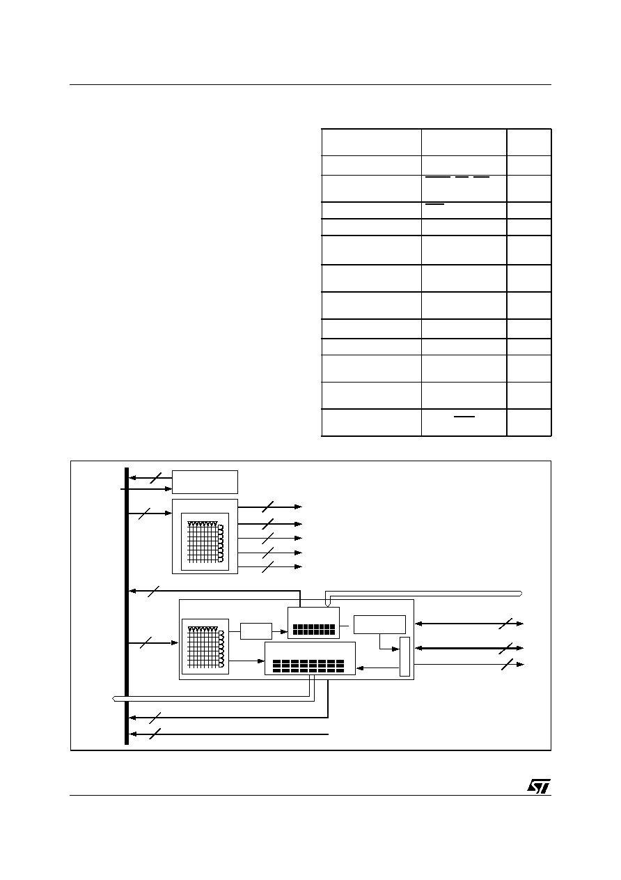
uPSD33XX
84/129
PLDS
The PLDs bring programmable logic functionality
to the uPSD. After specifying the logic for the
PLDs in PSDsoft Express, the logic is pro-
grammed into the device and available upon Pow-
er-up.
The PSD Module contains two PLDs: the Decode
PLD (DPLD), and the Complex PLD (CPLD).
The DPLD performs address decoding for Select
signals for PSD Module components, such as
memory, registers, and I/O ports.
The CPLD can be used for logic functions, such as
loadable counters and shift registers, state ma-
chines, and encoding and decoding logic.
The Turbo Bit in PSD Module
The PLDs can minimize power consumption by
switching off when inputs remain unchanged for
an extended time of about 70ns. Resetting the
Turbo Bit to '0' (Bit 3 of PMMR0) automatically
places the PLDs into standby if no inputs are
changing. Turning the Turbo Mode off increases
propagation delays while reducing power con-
sumption. See POWER MANAGEMENT, page 96
for details on setting the Turbo Bit.
Table 85. DPLD and CPLD Inputs
Note: 1. These inputs are not available in the 52-pin package.
Figure 38. PLD Diagram
Note: 1. Ports A is not available in the 52-pin package
Input Source
Input Name
No. of
Signals
MCU Address Bus
A15-A0
16
MCU Control Signals
PSEN, RD, WR,
ALE
4
RESET
RST
1
Power-down PDN
1
Port A Input
Macrocells
(1)
PA7-PA0 8
Port B Input
Macrocells
PB7-PB0 8
Port C Input
Macrocells
PC2-4, PC7
4
Port D Inputs
PD2-PD1 2
Page Register
PGR7-PGR0
8
Macrocell AB
Feedback
MCELLAB.FB7-
FB0
8
Macrocell BC
Feedback
MCELLBC.FB7-
FB0
8
Flash memory
Program Status Bit
Ready/Busy
1
PLD INPUT BUS
8
INPUT MACROCELL & INPUT PORTS
DIRECT MACROCELL INPUT TO MCU DATA BUS
CSIOP SELECT
SRAM SELECT
SECONDARY NON-VOLATILE MEMORY SELECTS
DECODE PLD
PAGE
REGISTER
PERIPHERAL SELECTS
CPLD
PT
ALLOC.
MACROCELL
ALLOC.
MCELLAB
MCELLBC
DIRECT MACROCELL ACCESS FROM MCU DATA BUS
20 INPUT MACROCELL
(PORT A,B,C)
16 OUTPUT
MACROCELL
I/O PORTS
PRIMARY FLASH MEMORY SELECTS
2
PORT D INPUTS
TO PORT A OR B(1)
TO PORT B OR C
DATA
BUS
8
8
8
4
1
1
2
EXTERNAL CHIP SELECTS
TO PORT D
2
16
20
OUTPUT MACROCELL FEEDBACK
AI06600
73
73
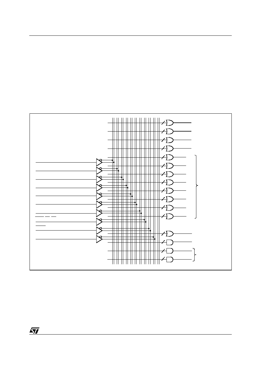
85/129
uPSD33XX
Decode PLD (DPLD)
The DPLD, shown in Figure 39, is used for decod-
ing the address for PSD Module and external com-
ponents. The DPLD can be used to generate the
following decode signals:
s
Up to 8 Sector Select (FS0-FS7) signals for the
primary Flash memory (three product terms
each).
s
Up to 4 Sector Select (CSBOOT0-CSBOOT3)
signals for the secondary Flash memory (three
product terms each)
s
1 internal SRAM Select (RS0) signal (two
product terms)
s
1 internal CSIOP Select signal (selects the PSD
Module registers)
s
2 internal Peripheral Select signals (Peripheral
I/O Mode).
Figure 39. DPLD Logic Array
Note: 1. Port A inputs are not available in the 52-pin package
2. Inputs from the MCU module
(INPUTS)
(20)
(8)
(16)
(1)
PDN (APD OUTPUT)
I /O PORTS (PORT A,B,C)1
(8)
PGR0 - PGR7
(8)
MCELLAB.FB [7:0] (FEEDBACKS)
MCELLBC.FB [7:0] (FEEDBACKS)
A[15:0]2
(2)
(4)
PD[2:1]
PSEN, RD, WR, ALE2
(1)
(1)
RESET
2
RD_BSY
RS0
CSIOP
PSEL0
PSEL1
8 PRIMARY FLASH
MEMORY SECTOR
SELECTS
SRAM SELECT
I/O DECODER
SELECT
PERIPHERAL I/O
MODE SELECT
CSBOOT 0
CSBOOT 1
CSBOOT 2
CSBOOT 3
FS0
FS7
3
3
3
3
3
3
3
3
3
3
3
3
2
AI06601
FS1
FS2
FS3
FS6
FS5
FS4
1
1
1

uPSD33XX
86/129
Complex PLD (CPLD)
The CPLD can be used to implement system logic
functions, such as loadable counters and shift reg-
isters, system mailboxes, handshaking protocols,
state machines, and random logic. The CPLD can
also be used to generate External Chip Select
(ECS1-ECS2), routed to Port D.
As shown in Figure 38, the CPLD has the following
blocks:
s
20 Input Macrocells (IMC)
s
16 Output Macrocells (OMC)
s
Macrocell Allocator
s
Product Term Allocator
s
AND Array capable of generating up to 137
product terms
s
Four I/O Ports.
Each of the blocks are described in the sections
that follow.
The Input Macrocells (IMC) and Output Macrocells
(OMC) are connected to the PSD Module internal
data bus and can be directly accessed by the
MCU. This enables the MCU software to load data
into the Output Macrocells (OMC) or read data
from both the Input and Output Macrocells (IMC
and OMC).
This feature allows efficient implementation of sys-
tem logic and eliminates the need to connect the
data bus to the AND Array as required in most
standard PLD macrocell architectures.
Figure 40. Macrocell and I/O Port
I/O PORTS
CPLD MACROCELLS
INPUT MACROCELLS
LATCHED
ADDRESS OUT
MUX
MUX
MUX
MUX
MUX
D
D
Q
Q
Q
G
D
Q D
WR
WR
PDR
DATA
PRODUCT TERM
ALLOCATOR
DIR
REG.
SELECT
INPUT
PRODUCT TERMS
FROM OTHER
MACROCELLS
POLARITY
SELECT
UP TO 10
PRODUCT TERMS
CLOCK
SELECT
PR
DI LD
D/T
CK
CL
Q
D/T/JK FF
SELECT
PT CLEAR
PT
CLOCK
GLOBAL
CLOCK
PT OUTPUT ENABLE (OE)
MACROCELL FEEDBACK
I/O PORT INPUT
ALE
PT INPUT LATCH GATE/CLOCK
MCU LOAD
PT PRESET
MCU DATA IN
COMB.
/REG
SELECT
MACROCELL
TO
I/O PORT
ALLOC.
CPLD
OUTPUT
TO OTHER I/O PORTS
PLD INPUT BUS
PLD INPUT BUS
MCU ADDRESS / DATA BUS
MACROCELL
OUT TO
MCU
DATA
LOAD
CONTROL
AND ARRAY
CPLD OUTPUT
I/O PIN
AI06602

87/129
uPSD33XX
Output Macrocell (OMC)
Eight of the Output Macrocells (OMC) are con-
nected to Ports A and B pins and are named as
McellAB0-McellAB7. The other eight macrocells
are connected to Ports B and C pins and are
named as McellBC0-McellBC7. If an McellAB out-
put is not assigned to a specific pin in PSDsoft, the
Macrocell Allocator block assigns it to either Port A
or B. The same is true for a McellBC output on Port
B or C. Table 86 shows the macrocells and port
assignment.
The Output Macrocell (OMC) architecture is
shown in Figure 41.
The flip-flop in the Output Macrocell (OMC) block
can be configured as a D, T, JK, or SR type in PS-
Dsoft. The flip-flop's clock, preset, and clear inputs
may be driven from a product term of the AND Ar-
ray. Alternatively, CLKIN (PD1) can be used for
the clock input to the flip-flop. The flip-flop is
clocked on the rising edge of CLKIN (PD1). The
preset and clear are active High inputs. Each clear
input can use up to two product terms.
Table 86. Output Macrocell Port and Data Bit Assignments
Note: 1. McellAB0-McellAB7 can only be assigned to Port B in the 52-pin package.
2. Port PC0, PC1, PC5, and PC6 are assigned to JTAG pins and are not available as Macrocell outputs.
Output
Macrocell
Port
Assignment
(1,2)
Native Product Terms
Maximum Borrowed
Product Terms
Data Bit for Loading or
Reading
McellAB0
Port A0, B0
3
6
D0
McellAB1
Port A1, B1
3
6
D1
McellAB2
Port A2, B2
3
6
D2
McellAB3
Port A3, B3
3
6
D3
McellAB4
Port A4, B4
3
6
D4
McellAB5
Port A5, B5
3
6
D5
McellAB6
Port A6, B6
3
6
D6
McellAB7
Port A7, B7
3
6
D7
McellBC0
Port B0
4
5
D0
McellBC1
Port B1
4
5
D1
McellBC2
Port B2, C2
4
5
D2
McellBC3
Port B3, C3
4
5
D3
McellBC4
Port B4, C4
4
6
D4
McellBC5
Port B5
4
6
D5
McellBC6
Port B6
4
6
D6
McellBC7
Port B7, C7
4
6
D7

uPSD33XX
88/129
Product Term Allocator
The CPLD has a Product Term Allocator. PSDsoft
uses the Product Term Allocator to borrow and
place product terms from one macrocell to anoth-
er. The following list summarizes how product
terms are allocated:
s
McellAB0-McellAB7 all have three native
product terms and may borrow up to six more
s
McellBC0-McellBC3 all have four native product
terms and may borrow up to five more
s
McellBC4-McellBC7 all have four native product
terms and may borrow up to six more.
Each macrocell may only borrow product terms
from certain other macrocells.
Loading and Reading the Output Macrocells
(OMC). The Output Macrocells (OMC) block oc-
cupies a memory location in the MCU address
space, as defined by the CSIOP block (see "I/O
PORTS (PSD MODULE), page 90). The flip-flops
in each of the 16 Output Macrocells (OMC) can be
loaded from the data bus by a MCU. Loading the
Output Macrocells (OMC) with data from the MCU
takes priority over internal functions. As such, the
preset, clear, and clock inputs to the flip-flop can
be overridden by the MCU. The ability to load the
flip-flops and read them back is useful in such ap-
plications as loadable counters and shift registers,
mailboxes, and handshaking protocols.
Data can be loaded to the Output Macrocells
(OMC) on the trailing edge of WRITE Strobe (WR,
edge loading) or during the time that WRITE
Strobe (WR) is active (level loading). The method
of loading is specified in PSDsoft Express Config-
uration.
Figure 41. CPLD Output Macrocell
PT
ALLOCATOR
MASK
REG.
PT CLK
PT
PT
PT
CLKIN
FEEDBACK (.FB)
PORT INPUT
AND ARRAY
PLD INPUT BUS
MUX
MUX
POLARITY
SELECT
LD
IN
CLR
Q
PR
DIN
COMB/REG
SELECT
PORT
DRIVER
INPUT
MACROCELL
I/O PIN
MACROCELL
ALLOCATOR
MCU DATA BUS
D [ 7:0]
DIRECTION
REGISTER
CLEAR (.RE)
PROGRAMMABLE
FF (D / T/JK /SR)
WR
ENABLE (.OE)
PRESET(.PR)
RD
MACROCELL CS
AI06617

89/129
uPSD33XX
The OMC Mask Register. There is one Mask
Register for each of the two groups of eight Output
Macrocells (OMC). The Mask Registers can be
used to block the loading of data to individual Out-
put Macrocells (OMC). The default value for the
Mask Registers is 00h, which allows loading of the
Output Macrocells (OMC). When a given bit in a
Mask Register is set to a '1,' the MCU is blocked
from writing to the associated Output Macrocells
(OMC). For example, suppose McellAB0-
McellAB3 are being used for a state machine. You
would not want a MCU write to McellAB to over-
write the state machine registers. Therefore, you
would want to load the Mask Register for McellAB
(Mask Macrocell AB) with the value 0Fh.
The Output Enable of the OMC. The Output
Macrocells (OMC) block can be connected to an I/
O port pin as a PLD output. The output enable of
each port pin driver is controlled by a single prod-
uct term from the AND Array, ORed with the Direc-
tion Register output. The pin is enabled upon
Power-up if no output enable equation is defined
and if the pin is declared as a PLD output in PSD-
soft Express.
If the Output Macrocell (OMC) output is declared
as an internal node and not as a port pin output in
the PSDabel file, the port pin can be used for other
I/O functions. The internal node feedback can be
routed as an input to the AND Array.
Input Macrocells (IMC)
The CPLD has 20 Input Macrocells (IMC), one for
each pin on Ports A and B, and 4 on Port C. The
architecture of the Input Macrocells (IMC) is
shown in Figure 42. The Input Macrocells (IMC)
are individually configurable, and can be used as
a latch, register, or to pass incoming Port signals
prior to driving them onto the PLD input bus. The
outputs of the Input Macrocells (IMC) can be read
by the MCU through the internal data bus.
The enable for the latch and clock for the register
are driven by a multiplexer whose inputs are a
product term from the CPLD AND Array or the
MCU Address Strobe (ALE). Each product term
output is used to latch or clock four Input Macro-
cells (IMC). Port inputs 3-0 can be controlled by
one product term and 7-4 by another.
Figure 42. Input Macrocell
OUTPUT
MACROCELLS BC
AND
MACROCELL AB
PT
PT
FEEDBACK
AND ARRAY
PLD INPUT BUS
PORT
DRIVER
I/O PIN
MCU DATA BUS
D [ 7: 0]
DIRECTION
REGISTER
MUX
MUX
ALE
PT
Q
Q
D
D
G
LATCH
INPUT MACROCELL
ENABLE (.OE)
D FF
INPUT MACROCELL _ RD
AI06603

uPSD33XX
90/129
I/O PORTS (PSD MODULE)
There are four programmable I/O ports: Ports A, B,
C, and D in the PSD Module. Each of the ports is
eight bits except Port D. Each port pin is individu-
ally user configurable, thus allowing multiple func-
tions per port. The ports are configured using
PSDsoft Express Configuration or by the MCU
writing to on-chip registers in the CSIOP space.
Port A is not available in the 52-pin package.
General Port Architecture
The general architecture of the I/O Port block is
shown in Figure 43. In general, once the purpose
for a port pin has been defined, that pin is no long-
er available for other purposes. Exceptions are
noted.
As shown in Figure 43, the ports contain an output
multiplexer whose select signals are driven by the
configuration bits in the Control Registers (Ports A
and B only) and PSDsoft Express Configuration.
Inputs to the multiplexer include the following:
s
Output data from the Data Out register
s
Latched address outputs
s
CPLD macrocell output
s
External Chip Select (ECS1-ECS2) from the
CPLD.
The Port Data Buffer (PDB) is a tri-state buffer that
allows only one source at a time to be read. The
Port Data Buffer (PDB) is connected to the Internal
Data Bus for feedback and can be read by the
MCU. The Data Out and macrocell outputs, Direc-
tion and Control Registers, and port pin input are
all connected to the Port Data Buffer (PDB).
Figure 43. General I/O Port Architecture
Note: 1. Control Register is not available in Ports C and D.
MCU D
A
T
A
B
U
S
DATA OUT
REG.
D
Q
D
G
Q
D
Q
D
Q
WR
WR
WR
ADDRESS
MACROCELL OUTPUTS
ENABLE PRODUCT TERM (.OE)
EXT CS
ALE
READ MUX
P
D
B
CPLD-INPUT
CONTROL REG.
(1)
DIR REG.
INPUT
MACROCELL
ENABLE OUT
DATA IN
OUTPUT
SELECT
OUTPUT
MUX
PORT PIN
DATA OUT
ADDRESS
AI07873

91/129
uPSD33XX
The Port pin's tri-state output driver enable is con-
trolled by a two input OR gate whose inputs come
from the CPLD AND Array enable product term
and the Direction Register. If the enable product
term of any of the Array outputs are not defined
and that port pin is not defined as a CPLD output
in the PSDsoft, then the Direction Register has
sole control of the buffer that drives the port pin.
The contents of these registers can be altered by
the MCU. The Port Data Buffer (PDB) feedback
path allows the MCU to check the contents of the
registers.
Ports A, B, and C have embedded Input Macro-
cells (IMC). The Input Macrocells (IMC) can be
configured as latches, registers, or direct inputs to
the PLDs. The latches and registers are clocked
by Address Strobe (ALE) or a product term from
the PLD AND Array. The outputs from the Input
Macrocells (IMC) drive the PLD input bus and can
be read by the MCU. See Input Macrocell, page
89.
Port Operating Modes
The I/O Ports have several modes of operation.
Some modes can be defined using PSDsoft, some
by the MCU writing to the Control Registers in
CSIOP space, and some by both. The modes that
can only be defined using PSDsoft must be pro-
grammed into the device and cannot be changed
unless the device is reprogrammed. The modes
that can be changed by the MCU can be done so
dynamically at run-time. The PLD I/O, Data Port,
Address Input, and Peripheral I/O Modes are the
only modes that must be defined before program-
ming the device. All other modes can be changed
by the MCU at run-time. See Application Note
AN1171
for more detail.
Table 87 summarizes which modes are available
on each port. Table 90 shows how and where the
different modes are configured. Each of the port
operating modes are described in the following
sections.
MCU I/O Mode
In the MCU I/O Mode, the MCU uses the I/O Ports
block to expand its own I/O ports. By setting up the
CSIOP space, the ports on the PSD Module are
mapped into the MCU address space. The ad-
dresses of the ports are listed in Table 78, page
73.
A port pin can be put into MCU I/O Mode by writing
a '0' to the corresponding bit in the Control Regis-
ter. The MCU I/O direction may be changed by
writing to the corresponding bit in the Direction
Register, or by the output enable product term
(see Peripheral I/O Mode, page 91). When the pin
is configured as an output, the content of the Data
Out Register drives the pin. When configured as
an input, the MCU can read the port input through
the Data In buffer. See Figure 43, page 90.
Ports C and D do not have Control Registers, and
are in MCU I/O Mode by default. They can be used
for PLD I/O if equations are written for them in PS-
Dabel.
PLD I/O Mode
The PLD I/O Mode uses a port as an input to the
CPLD's Input Macrocells (IMC), and/or as an out-
put from the CPLD's Output Macrocells (OMC).
The output can be tri-stated with a control signal.
This output enable control signal can be defined
by a product term from the PLD, or by resetting the
corresponding bit in the Direction Register to '0.'
The corresponding bit in the Direction Register
must not be set to '1' if the pin is defined for a PLD
input signal in PSDsoft. The PLD I/O Mode is
specified in PSDsoft by declaring the port pins,
and then writing an equation assigning the PLD I/
O to a port.
Address Out Mode
Address Out Mode can be used to drive latched
MCU addresses on to the port pins. These port
pins can, in turn, drive external devices. Either the
output enable or the corresponding bits of both the
Direction Register and Control Register must be
set to a '1' for pins to use Address Out Mode. This
must be done by the MCU at run-time. See Table
89 for the address output pin assignments on
Ports A and B for various MCUs.
Peripheral I/O Mode
Peripheral I/O Mode can be used to interface with
external peripherals. In this mode, all of Port A
serves as a tri-state, bi-directional data buffer for
the MCU. Peripheral I/O Mode is enabled by set-
ting Bit 7 of the VM Register to a '1.' Figure 44
shows how Port A acts as a bi-directional buffer for
the MCU data bus if Peripheral I/O Mode is en-
abled. An equation for PSEL0 and/or PSEL1 must
be written in PSDsoft. The buffer is tri-stated when
PSEL0 or PSEL1 is low (not active). The PSEN
signal should be "ANDed" in the PSEL equations
to disable the buffer when PSEL resides in the
data space.
JTAG In-System Programming (ISP)
Port C is JTAG compliant, and can be used for In-
System Programming (ISP). For more information
on the JTAG Port, see PROGRAMMING IN-CIR-
CUIT USING THE JTAG SERIAL INTERFACE,
page 101.

uPSD33XX
92/129
Figure 44. Peripheral I/O Mode
Table 87. Port Operating Modes
Note: 1. Port A is not available in the 52-pin package.
2. On pins PC2, PC3, PC4, and PC7 only.
3. JTAG pins (TMS, TCK, TDI, TDO) are dedicated pins.
Table 88. Port Operating Mode Settings
Note: 1. N/A = Not Applicable
2. The direction of the Port A,B,C, and D pins are controlled by the Direction Register ORed with the individual output enable product
term (.oe) from the CPLD AND Array.
Table 89. I/O Port Latched Address Output Assignments
Port Mode
Port A
(1)
Port B
Port C
Port D
MCU I/O
Yes
Yes
Yes
Yes
PLD I/O
McellAB Outputs
McellBC Outputs
Additional Ext. CS Outputs
PLD Inputs
Yes
No
No
Yes
Yes
Yes
No
Yes
No
Yes
(2)
No
Yes
No
No
Yes
Yes
Address Out
Yes (A7 ≠ 0)
Yes (A7 ≠ 0)
No
No
Peripheral I/O
Yes
No
No
No
JTAG ISP
No
No
Yes
(3)
No
Mode
Defined in PSDsoft
Control Register
Setting
(1)
Direction Register
Setting
(1)
VM Register Setting
(1)
MCU I/O
Declare pins only
0
1 = output,
0 = input (Note 2)
N/A
PLD I/O
Logic equations
N/A
(Note
2)
N/A
Address Out
(Port A,B)
Declare pins only
1
1 (Note
2)
N/A
Peripheral I/O
(Port A)
Logic equations
(PSEL0 & 1)
N/A
N/A
PIO Bit = 1
Port A (PA3-PA0)
Port A (PA7-PA4)
Port B (PB3-PB0)
Port B (PB7-PB4)
Address
a3-a0 Address
a7-a4 Address
a3-a0 Address
a7-a4
RD
PSEL0
PSEL1
PSEL
VM REGISTER BIT 7
WR
PA0 - PA7
D0 - D7
DATA BUS
AI02886

93/129
uPSD33XX
Port Configuration Registers (PCR)
Each Port has a set of Port Configuration Regis-
ters (PCR) used for configuration. The contents of
the registers can be accessed by the MCU through
normal READ/WRITE bus cycles at the addresses
given in Table 78, page 73. The addresses in Ta-
ble 80, page 75 are the offsets in hexadecimal
from the base of the CSIOP register.
The pins of a port are individually configurable and
each bit in the register controls its respective pin.
For example, Bit 0 in a register refers to Bit 0 of its
port. The three Port Configuration Registers
(PCR), shown in Table 90, are used for setting the
Port configurations. The default Power-up state for
each register in Table 90 is 00h.
Control Register. Any bit reset to '0' in the Con-
trol Register sets the corresponding port pin to
MCU I/O Mode, and a '1' sets it to Address Out
Mode. The default mode is MCU I/O. Only Ports A
and B have an associated Control Register.
Direction Register. The Direction Register, in
conjunction with the output enable (except for Port
D), controls the direction of data flow in the I/O
Ports. Any bit set to '1' in the Direction Register
causes the corresponding pin to be an output, and
any bit set to '0' causes it to be an input. The de-
fault mode for all port pins is input.
Figure 43, page 90 shows the Port Architecture di-
agrams for Ports A/B and C, respectively. The di-
rection of data flow for Ports A, B, and C are
controlled not only by the direction register, but
also by the output enable product term from the
PLD AND Array. If the output enable product term
is not active, the Direction Register has sole con-
trol of a given pin's direction.
An example of a configuration for a Port with the
three least significant bits set to output and the re-
mainder set to input is shown in Table 93. Since
Port D only contains two pins, the Direction Regis-
ter for Port D has only two bits active.
Drive Select Register. The Drive Select Register
configures the pin driver as Open Drain or CMOS
for some port pins, and controls the slew rate for
the other port pins. An external pull-up resistor
should be used for pins configured as Open Drain.
A pin can be configured as Open Drain if its corre-
sponding bit in the Drive Select Register is set to a
'1.' The default pin drive is CMOS.
Note: The slew rate is a measurement of the rise
and fall times of an output. A higher slew rate
means a faster output response and may create
more electrical noise. A pin operates in a high slew
rate when the corresponding bit in the Drive Reg-
ister is set to '1.' The default rate is slow slew.
Table 94, page 94 shows the Drive Register for
Ports A, B, C, and D. It summarizes which pins can
be configured as Open Drain outputs and which
pins the slew rate can be set for.
Table 90. Port Configuration Registers (PCR)
Note: 1. See Table 94 for Drive Register Bit definition.
Table 91. Port Pin Direction Control, Output
Enable P.T. Not Defined
Table 92. Port Pin Direction Control, Output
Enable P.T. Defined
Table 93. Port Direction Assignment Example
Register Name
Port
MCU Access
Control
A,B
WRITE/READ
Direction
A,B,C,D
WRITE/READ
Drive Select
(1)
A,B,C,D
WRITE/READ
Direction Register Bit
Port Pin Mode
0 Input
1 Output
Direction
Register Bit
Output Enable
P.T.
Port Pin Mode
0 0 Input
0 1 Output
1 0 Output
1 1 Output
Bit 7 Bit 6 Bit 5
Bit 4 Bit 3
Bit 2
Bit 1
Bit 0
0 0 0 0 0 1 1 1

uPSD33XX
94/129
Port Data Registers
The Port Data Registers, shown in Table 95, are
used by the MCU to write data to or read data from
the ports. Table 95 shows the register name, the
ports having each register type, and MCU access
for each register type. The registers are described
below.
Data In. Port pins are connected directly to the
Data In buffer. In MCU I/O Input Mode, the pin in-
put is read through the Data In buffer.
Data Out Register. Stores output data written by
the MCU in the MCU I/O Output Mode. The con-
tents of the Register are driven out to the pins if the
Direction Register or the output enable product
term is set to '1.' The contents of the register can
also be read back by the MCU.
Output Macrocells (OMC). The CPLD Output
Macrocells (OMC) occupy a location in the MCU's
address space. The MCU can read the output of
the Output Macrocells (OMC). If the OMC Mask
Register Bits are not set, writing to the macrocell
loads data to the macrocell flip-flops. See PLDs,
page 84.
OMC Mask Register. Each OMC Mask Register
Bit corresponds to an Output Macrocell (OMC) flip-
flop. When the OMC Mask Register Bit is set to a
'1,' loading data into the Output Macrocell (OMC)
flip-flop is blocked. The default value is '0' or un-
blocked.
Input Macrocells (IMC). The Input Macrocells
(IMC) can be used to latch or store external inputs.
The outputs of the Input Macrocells (IMC) are rout-
ed to the PLD input bus, and can be read by the
MCU. See PLDs, page 84.
Enable Out. The Enable Out register can be read
by the MCU. It contains the output enable values
for a given port. A '1' indicates the driver is in out-
put mode. A '0' indicates the driver is in tri-state
and the pin is in input mode.
Table 94. Drive Register Pin Assignment
Note: 1. NA = Not Applicable.
Table 95. Port Data Registers
Drive
Register
Bit 7
Bit 6
Bit 5
Bit 4
Bit 3
Bit 2
Bit 1
Bit 0
Port A
Open
Drain
Open
Drain
Open
Drain
Open
Drain
Slew
Rate
Slew
Rate
Slew
Rate
Slew
Rate
Port B
Open
Drain
Open
Drain
Open
Drain
Open
Drain
Slew
Rate
Slew
Rate
Slew
Rate
Slew
Rate
Port C
Open
Drain
Open
Drain
Open
Drain
Open
Drain
Open
Drain
Open
Drain
Open
Drain
Open
Drain
Port D
NA
(1)
NA
(1)
NA
(1)
NA
(1)
NA
(1)
Slew
Rate
Slew
Rate
NA
(1)
Register Name
Port
MCU Access
Data In
A,B,C,D
READ ≠ input on pin
Data Out
A,B,C,D
WRITE/READ
Output Macrocell
A,B,C
READ ≠ outputs of macrocells
WRITE ≠ loading macrocells flip-flop
Mask Macrocell
A,B,C
WRITE/READ ≠ prevents loading into a given
macrocell
Input Macrocell
A,B,C
READ ≠ outputs of the Input Macrocells
Enable Out
A,B,C
READ ≠ the output enable control of the port driver

95/129
uPSD33XX
Ports A and B ≠ Functionality and Structure
Ports A and B have similar functionality and struc-
ture, as shown in Figure 43, page 90. The two
ports can be configured to perform one or more of
the following functions:
s
MCU I/O Mode
s
CPLD Output ≠ Macrocells McellAB7-McellAB0
can be connected to Port A or Port B. McellBC7-
McellBC0 can be connected to Port B or Port C.
s
CPLD Input ≠ Via the Input Macrocells (IMC).
s
Latched Address output ≠ Provide latched
address output as per Table 89.
s
Open Drain/Slew Rate ≠ pins PA3-PA0 and
PB3-PB0 can be configured to fast slew rate,
pins PA7-PA4 and PB7-PB4 can be configured
to Open Drain Mode.
s
Peripheral Mode ≠ Port A only (80-pin package)
Port C ≠ Functionality and Structure
Port C can be configured to perform one or more
of the following functions (see Figure 43, page 90):
s
MCU I/O Mode
s
CPLD Output ≠ McellBC[2, 3. 4, 7] outputs can
be connected to Port C.
s
CPLD Input ≠ via the Input Macrocells (IMC) on
pins PC2, PC3, PC4, and PC7.
s
In-System Programming (ISP) ≠ Port pins PC0,
PC1, PC5, and PC6 are dedicated for JTAG ISP
programming (TMS, TCK, TDI, TDO, see
PROGRAMMING IN-CIRCUIT USING THE
JTAG SERIAL INTERFACE, page 101, for
more information on JTAG programming.)
s
Open Drain ≠ Port C pins can be configured in
Open Drain Mode
s
Battery Backup features ≠ PC2 can be
configured for a battery input supply, Voltage
Stand-by (V
STBY
).
PC4 can be configured as a Battery-on Indicator
(V
BATON
), indicating when V
CC
is less than
V
BAT
.
Port D ≠ Functionality and Structure
Port D has two I/O pins (only one pin, PD1, in the
52-pin package). This port does not support Ad-
dress Out Mode, and therefore no Control Regis-
ter is required. Of the eight bits in the Port D
registers, only Bits 2 and 1 are used to configure
pins PD2 and PD1.
Port D can be configured to perform one or more
of the following functions:
s
MCU I/O Mode;
s
CPLD Output ≠ External Chip Select (ECS1-
ECS2), each ECS consists of one product term
that can be configured active high or low;
s
CPLD Input ≠ direct input to the CPLD, no Input
Macrocells (IMC); and
s
Slew rate ≠ pins can be set up for fast slew rate
Port D pins can be configured in PSDsoft Express
as input pins for other dedicated functions:
s
CLKIN (PD1) as input to the macrocells flip-
flops and APD counter, and
s
PSD Chip Select Input (CSI, PD2). Driving this
signal High disables the Flash memory, SRAM
and CSIOP.

uPSD33XX
96/129
POWER MANAGEMENT
All PSD Module offers configurable power saving
options. These options may be used individually or
in combinations, as follows:
s
The primary and secondary Flash memory, and
SRAM blocks are built with power management
technology. In addition to using special silicon
design methodology, power management
technology puts the memories into Standby
Mode when address/data inputs are not
changing (zero DC current). As soon as a
transition occurs on an input, the affected
memory "wakes up," changes and latches its
outputs, then goes back to standby. The
designer does
not
have to do anything special to
achieve Memory Standby Mode when no inputs
are changing--it happens automatically.
The PLD sections can also achieve Standby
Mode when its inputs are not changing, as
described in the sections on the Power
Management Mode Registers (PMMR).
s
As with the Power Management Mode, the
Automatic Power Down (APD) block allows the
PSD Module to reduce to stand-by current
automatically. The APD Unit can also block
MCU address/data signals from reaching the
memories and PLDs.
Built in logic monitors the Address Strobe of the
MCU for activity. If there is no activity for a
certain time period (MCU is asleep), the APD
Unit initiates Power-down Mode (if enabled).
Once in Power-down Mode, all address/data
signals are blocked from reaching memory and
PLDs, and the memories are deselected
internally. This allows the memory and PLDs to
remain in Standby Mode even if the address/
data signals are changing state externally
(noise, other devices on the MCU bus, etc.).
Keep in mind that any unblocked PLD input
signals that are changing states keeps the PLD
out of Stand-by Mode, but not the memories.
s
PSD Chip Select Input (CSI, PD2) can be used
to disable the internal memories, placing them
in Standby Mode even if inputs are changing.
This feature does not block any internal signals
or disable the PLDs. This is a good alternative
to using the APD Unit. There is a slight penalty
in memory access time when PSD Chip Select
Input (CSI, PD2) makes its initial transition from
deselected to selected.
s
The PMMRs can be written by the MCU at run-
time to manage power. The PSD Module
supports "blocking bits" in these registers that
are set to block designated signals from
reaching both PLDs. Current consumption of
the PLDs is directly related to the composite
frequency of the changes on their inputs (see
Figure 48 and Figure 49). Significant power
savings can be achieved by blocking signals
that are not used in DPLD or CPLD logic
equations.
Figure 45. APD Unit
APD EN
PMMR0 BIT 1=1
ALE
RESET
CSI
CLKIN
TRANSITION
DETECTION
EDGE
DETECT
APD
COUNTER
POWER DOWN
(PDN)
DISABLE BUS
INTERFACE
CSIOP SELECT
FLASH SELECT
SRAM SELECT
PD
CLR
PD
DISABLE
FLASH/SRAM
PLD
SELECT
AI06608

97/129
uPSD33XX
The PSD Module has a Turbo Bit in PMMR0.This
bit can be set to turn the Turbo Mode off (the de-
fault is with Turbo Mode turned on). While Turbo
Mode is off, the PLDs can achieve standby current
when no PLD inputs are changing (zero DC cur-
rent). Even when inputs do change, significant
power can be saved at lower frequencies (AC cur-
rent), compared to when Turbo Mode is on. When
the Turbo Mode is on, there is a significant DC cur-
rent component and the AC component is higher.
Automatic Power-down (APD) Unit and Power-
down Mode. The APD Unit, shown in Figure 45,
puts the PSD Module into Power-down Mode by
monitoring the activity of Address Strobe (ALE). If
the APD Unit is enabled, as soon as activity on Ad-
dress Strobe (ALE) stops, a four-bit counter starts
counting. If Address Strobe (ALE/AS, PD0) re-
mains inactive for fifteen clock periods of CLKIN
(PD1), Power-down (PDN) goes High, and the
PSD Module enters Power-down Mode, as dis-
cussed next.
Power-down Mode. By default, if you enable the
APD Unit, Power-down Mode is automatically en-
abled. The device enters Power-down Mode if Ad-
dress Strobe (ALE) remains inactive for fifteen
periods of CLKIN (PD1).
The following should be kept in mind when the
PSD Module is in Power-down Mode:
s
If Address Strobe (ALE) starts pulsing again, the
PSD Module returns to normal Operating mode.
The PSD Module also returns to normal
Operating mode if either PSD Chip Select Input
(CSI, PD2) is Low or the RESET input is High.
s
The MCU address/data bus is blocked from all
memory and PLDs.
s
Various signals can be blocked (prior to Power-
down Mode) from entering the PLDs by setting
the appropriate bits in the PMMR registers. The
blocked signals include MCU control signals
and the common CLKIN (PD1).
Note: Blocking CLKIN (PD1) from the PLDs
does not block CLKIN (PD1) from the APD Unit.
s
All memories enter Standby Mode and are
drawing standby current. However, the PLD and
I/O ports blocks do
not
go into Standby Mode
because you don't want to have to wait for the
logic and I/O to "wake-up" before their outputs
can change. See Table 96 for Power-down
Mode effects on PSD Module ports.
s
Typical standby current is of the order of
microamperes. These standby current values
assume that there are no transitions on any PLD
input.
Other Power Saving Options. The PSD Module
offers other reduced power saving options that are
independent of the Power-down Mode. Except for
the SRAM Stand-by and PSD Chip Select Input
(CSI, PD2) features, they are enabled by setting
bits in PMMR0 and PMMR2.
Figure 46. Enable Power-down Flow Chart
Table 96. Power-down Mode's Effect on Ports
Port Function
Pin Level
MCU I/O
No Change
PLD Out
No Change
Address Out
Undefined
Peripheral I/O
Tri-State
Enable APD
Set PMMR0 Bit 1 = 1
PSD Module in Power
Down Mode
ALE idle
for 15 CLKIN
clocks?
RESET
Yes
No
OPTIONAL
Disable desired inputs to PLD
by setting PMMR0 bits 4 and 5
and PMMR2 bits 2 through 6.
AI06609
uPSD33XX
98/129
PLD Power Management
The power and speed of the PLDs are controlled
by the Turbo Bit (Bit 3) in PMMR0. By setting the
bit to '1,' the Turbo Mode is off and the PLDs con-
sume the specified stand-by current when the in-
puts are not switching for an extended time of
70ns. The propagation delay time is increased by
10ns (for a 5V device) after the Turbo Bit is set to
'1' (turned off) when the inputs change at a com-
posite frequency of less than 15MHz. When the
Turbo Bit is reset to '0' (turned on), the PLDs run
at full power and speed. The Turbo Bit affects the
PLD's DC power, AC power, and propagation de-
lay. When the Turbo Mode is off, the uPSD3200
input clock frequency is reduced by 5MHz from the
maximum rated clock frequency.
Blocking MCU control signals with the bits of
PMMR2 can further reduce PLD AC power con-
sumption.
SRAM Standby Mode (Battery Backup). The
SRAM in the PSD Module supports a battery back-
up mode in which the contents are retained in the
event of a power loss. The SRAM has Voltage
Stand-by (V
STBY
, PC2) that can be connected to
an external battery. When V
CC
becomes lower
than V
STBY
then the SRAM automatically con-
nects to Voltage Stand-by (V
STBY
, PC2) as a pow-
er source. The SRAM Standby Current (I
STBY
) is
typically 0.5 uA. The SRAM data retention voltage
is 2V minimum. The Battery-on Indicator
(V
BATON
) can be routed to PC4. This signal indi-
cates when the V
CC
has dropped below V
STBY
.
PSD Chip Select Input (CSI, PD2)
PD2 of Port D can be configured in PSDsoft Ex-
press as PSD Chip Select Input (CSI). When Low,
the signal selects and enables the PSD Module
Flash memory, SRAM, and I/O blocks for READ or
WRITE operations. A High on PSD Chip Select In-
put (CSI, PD2) disables the Flash memory, and
SRAM, and reduces power consumption. Howev-
er, the PLD and I/O signals remain operational
when PSD Chip Select Input (CSI, PD2) is High.
Input Clock
CLKIN (PD1) can be turned off, to the PLD to save
AC power consumption. CLKIN (PD1) is an input
to the PLD AND Array and the Output Macrocells
(OMC).
During Power-down Mode, or, if CLKIN (PD1) is
not being used as part of the PLD logic equation,
the clock should be disabled to save AC power.
CLKIN (PD1) is disconnected from the PLD AND
Array or the Macrocells block by setting Bits 4 or 5
to a '1' in PMMR0.
Input Control Signals
The PSD Module provides the option to turn off the
MCU signals (WR, RD, PSEN, and Address
Strobe (ALE)) to the PLD to save AC power con-
sumption. These control signals are inputs to the
PLD AND Array. During Power-down Mode, or, if
any of them are not being used as part of the PLD
logic equation, these control signals should be dis-
abled to save AC power. They are disconnected
from the PLD AND Array by setting Bits 2, 3, 4, 5,
and 6 to a '1' in PMMR2.
Table 97. Power Management Mode Registers PMMR0
Bit 0
X
0
Not used, and should be set to zero.
Bit 1
APD Enable
0 = off Automatic Power-down (APD) is disabled.
1 = on Automatic Power-down (APD) is enabled.
Bit 2
X
0
Not used, and should be set to zero.
Bit 3
PLD Turbo
0 = on PLD Turbo Mode is on
1 = off
PLD Turbo Mode is off, saving power.
uPSD3200 operates at 5MHz below the maximum rated clock frequency
Bit 4
PLD Array clk
0 = on
CLKIN (PD1) input to the PLD AND Array is connected. Every change of CLKIN
(PD1) Powers-up the PLD when Turbo Bit is '0.'
1 = off CLKIN (PD1) input to PLD AND Array is disconnected, saving power.
Bit 5
PLD MCell clk
0 = on CLKIN (PD1) input to the PLD macrocells is connected.
1 = off CLKIN (PD1) input to PLD macrocells is disconnected, saving power.
Bit 6
X
0
Not used, and should be set to zero.
Bit 7
X
0
Not used, and should be set to zero.

99/129
uPSD33XX
Table 98. Power Management Mode Registers PMMR2
Note: The bits of this register are cleared to zero following Power-up. Subsequent RESET pulses do not clear the registers.
Table 99. APD Counter Operation
Bit 0
X
0
Not used, and should be set to zero.
Bit 1
X
0
Not used, and should be set to zero.
Bit 2
PLD Array
WR
0 = on WR input to the PLD AND Array is connected.
1 = off WR input to PLD AND Array is disconnected, saving power.
Bit 3
PLD Array
RD
0 = on RD input to the PLD AND Array is connected.
1 = off RD input to PLD AND Array is disconnected, saving power.
Bit 4
PLD Array
PSEN
0 = on PSEN input to the PLD AND Array is connected.
1 = off PSEN input to PLD AND Array is disconnected, saving power.
Bit 5
PLD Array
ALE
0 = on ALE input to the PLD AND Array is connected.
1 = off ALE input to PLD AND Array is disconnected, saving power.
Bit 6
X
0
Not used, and should be set to zero.
Bit 7
X
0
Not used, and should be set to zero.
APD Enable Bit
ALE Level
APD Counter
0 X
Not
Counting
1 Pulsing
Not
Counting
1
0 or 1
Counting (Generates PDN after 15 Clocks)
uPSD33XX
100/129
RESET TIMING AND DEVICE STATUS AT RESET
Upon Power-up, the PSD Module requires a Reset
(RESET) pulse of duration t
NLNH-PO
after V
CC
is
steady. During this period, the device loads inter-
nal configurations, clears some of the registers
and sets the Flash memory into operating mode.
The Flash memory is reset to the READ Mode
upon Power-up. Sector Select (FS0-FS7 and
CSBOOT0-CSBOOT3) must all be Low. Any
Flash memory WRITE cycle initiation is prevented
automatically when V
DD
is below V
LKO
.
Warm RESET
Once the device is up and running, the PSD Mod-
ule can be reset with a pulse of a much shorter du-
ration, t
NLNH
.
I/O Pin, Register and PLD Status at RESET
Table 100 shows the I/O pin, register and PLD sta-
tus during Power-on RESET, Warm RESET, and
Power-down Mode. PLD outputs are always valid
during Warm RESET, and they are valid in Power-
on RESET once the internal Configuration bits are
loaded. This loading is completed typically long
before the V
CC
ramps up to operating level. Once
the PLD is active, the state of the outputs are de-
termined by the PLD equations.
Reset of Flash Memory Erase and Program
Cycles
A Reset (RESET) also resets the internal Flash
memory state machine. During a Flash memory
Program or Erase cycle, Reset (RESET) termi-
nates the cycle and returns the Flash memory to
the READ Mode within a period of t
NLNH-A
.
Figure 47. Reset (RESET) Timing
Table 100. Status During Power-on RESET, Warm RESET and Power-down Mode
Note: 1. The SR_cod and PeriphMode Bits in the VM Register are always cleared to '0' on Power-on RESET or Warm RESET.
Port Configuration
Power-On RESET Warm
RESET Power-down
Mode
MCU I/O
Input mode
Input mode
Unchanged
PLD Output
Valid after internal PSD
configuration bits are
loaded
Valid
Depends on inputs to PLD
(addresses are blocked in
PD Mode)
Address
Out
Tri-stated Tri-stated Not
defined
Peripheral
I/O
Tri-stated Tri-stated Tri-stated
Register Power-On
RESET Warm
RESET Power-down
Mode
PMMR0 and PMMR2
Cleared to '0'
Unchanged
Unchanged
Macrocells flip-flop status
Cleared to '0' by internal
Power-on RESET
Depends on .re and .pr
equations
Depends on .re and .pr
equations
VM Register
(1)
Initialized, based on the
selection in PSDsoft
Configuration menu
Initialized, based on the
selection in PSDsoft
Configuration menu
Unchanged
All other registers
Cleared to '0'
Cleared to '0'
Unchanged
tNLNH-PO
AI07874
RESET
tNLNH
tNLNH-A
V
CC
V
CC
(min)
Power-On Reset
Warm Reset
101/129
uPSD33XX
PROGRAMMING IN-CIRCUIT USING THE JTAG SERIAL INTERFACE
The JTAG Serial Interface pins (TMS, TCK, TDI,
TDO) are dedicated pins on Port C (see Table
101). All memory blocks (primary and secondary
Flash memory), PLD logic, and PSD Module Con-
figuration Register Bits may be programmed
through the JTAG Serial Interface block. A blank
device can be mounted on a printed circuit board
and programmed using JTAG.
The standard JTAG signals (IEEE 1149.1) are
TMS, TCK, TDI, and TDO. Two additional signals,
TSTAT and TERR, are optional JTAG extensions
used to speed up Program and Erase cycles.
By default, on a blank device (as shipped from the
factory or after erasure), four pins on Port C are
the basic JTAG signals TMS, TCK, TDI, and TDO
.
Standard JTAG Signals
At power-up, the standard JTAG pins are inputs,
waiting for a JTAG serial command from an exter-
nal JTAG controller device (such as FlashLINK or
Automated Test Equipment). When the enabling
command is received, TDO becomes an output
and the JTAG channel is fully functional. The
same command that enables the JTAG channel
may optionally enable the two additional JTAG sig-
nals, TSTAT and TERR.
The RESET input to the uPS3200 should be active
during JTAG programming. The active RESET
puts the MCU module into RESET Mode while the
PSD Module is being programmed. See Applica-
tion Note AN1153 for more details on JTAG In-
System Programming (ISP).
The uPSD33XX Devices supports JTAG In-Sys-
tem-Configuration (ISC) commands, but not
Boundary Scan. The PSDsoft Express software
tool and FlashLINK JTAG programming cable im-
plement the JTAG In-System-Configuration (ISC)
commands.
Table 101. JTAG Port Signals
JTAG Extensions
TSTAT and TERR are two JTAG extension signals
enabled by an "ISC_ENABLE" command received
over the four standard JTAG signals (TMS, TCK,
TDI, and TDO). They are used to speed Program
and Erase cycles by indicating status on uPDS
signals instead of having to scan the status out se-
rially using the standard JTAG channel. See Appli-
cation Note
AN1153
.
TERR indicates if an error has occurred when
erasing a sector or programming a byte in Flash
memory. This signal goes Low (active) when an
Error condition occurs, and stays Low until an
"ISC_CLEAR" command is executed or a chip Re-
set (RESET) pulse is received after an
"ISC_DISABLE" command.
TSTAT behaves the same as Ready/Busy. TSTAT
is High when the PSD Module device is in READ
Mode (primary and secondary Flash memory con-
tents can be read). TSTAT is Low when Flash
memory Program or Erase cycles are in progress,
and also when data is being written to the second-
ary Flash memory.
TSTAT and TERR can be configured as open-
drain type signals during an "ISC_ENABLE" com-
mand.
Security and Flash Memory Protection
When the Security Bit is set, the device cannot be
read on a Device Programmer or through the
JTAG Port. When using the JTAG Port, only a Full
Chip Erase command is allowed.
All other Program, Erase, and Verify commands
are blocked. Full Chip Erase returns the part to a
non-secured, blank state. The Security Bit can be
set in PSDsoft Express Configuration.
All primary and secondary Flash memory sectors
can individually be sector protected against era-
sures. The sector protect bits can be set in PSD-
soft Express Configuration.
INITIAL DELIVERY STATE
When delivered from ST, the uPSD33XX Devices
have all bits in the memory and PLDs set to '1.'
The code, configuration, and PLD logic are loaded
using the programming procedure. Information for
programming the device is available directly from
ST. Please contact your local sales representa-
tive.
Port C Pin
JTAG Signals
Description
PC0
TMS
Mode Select
PC1
TCK
Clock
PC3
TSTAT
Status (optional)
PC4
TERR
Error flag (optional)
PC5
TDI
Serial Data In
PC6
TDO
Serial Data Out

uPSD33XX
102/129
AC/DC PARAMETERS
These tables describe the AD and DC parameters
of the uPSD33XX Devices:
s
DC Electrical Specification
s
AC Timing Specification
s
PLD Timing
≠ Combinatorial Timing
≠ Synchronous Clock Mode
≠ Asynchronous Clock Mode
≠ Input Macrocell Timing
s
MCU Module Timing
≠ READ Timing
≠ WRITE Timing
≠ Power-down and RESET Timing
The following are issues concerning the parame-
ters presented:
s
In the DC specification the supply current is
given for different modes of operation.
s
The AC power component gives the PLD, Flash
memory, and SRAM mA/MHz specification.
Figure 48 and Figure 49 show the PLD mA/MHz
as a function of the number of Product Terms
(PT) used.
s
In the PLD timing parameters, add the required
delay when Turbo Bit is '0.'
Figure 48. PLD I
CC
/Frequency Consumption (5V range)
Figure 49. PLD I
CC
/Frequency Consumption (3V range)
0
10
20
30
40
60
70
80
90
100
110
V
CC
= 5V
50
0
10
15
5
20 25
HIGHEST COMPOSITE FREQUENCY AT PLD INPUTS (MHz)
I
CC
≠ (mA)
TURBO ON (100%)
TURBO ON (25%)
TURBO OFF
TURBO OFF
PT 100%
PT 25%
AI02894
0
10
20
30
40
50
60
V
CC
= 3V
0
10
15
5
20 25
I
CC
≠ (mA)
TURBO ON (100%)
TURBO ON (25%)
TURBO OFF
TURBO OFF
HIGHEST COMPOSITE FREQUENCY AT PLD INPUTS (MHz)
PT 100%
PT 25%
AI03100

103/129
uPSD33XX
Table 102. PSD Module Example, Typ. Power Calculation at V
CC
= 5.0V (Turbo Mode Off)
Conditions
MCU Clock Frequency
= 12MHz
Highest Composite PLD input frequency
(Freq PLD)
= 8MHz
MCU ALE frequency (Freq ALE)
= 2MHz
% Flash memory
Access
= 80%
% SRAM access
= 15%
% I/O access
= 5% (no additional power above base)
Operational Modes
% Normal
= 40%
% Power-down Mode
= 60%
Number of product terms used
(from fitter report)
= 45 PT
% of total product terms
= 45/182 = 24.7%
Turbo Mode
= Off
Calculation (using typical values)
I
CC
total
= I
CC
(MCUactive) x %MCUactive + I
CC
(PSDactive) x %PSDactive + I
PD
(pwrdown) x %pwrdown
I
CC
(MCUactive)
= 20mA
I
PD
(pwrdown)
= 250uA
I
CC
(PSDactive)
= I
CC
(ac) + I
CC
(dc)
= %flash x 2.5 mA/MHz x Freq ALE
+ %SRAM x 1.5 mA/MHz x Freq ALE
+ % PLD x (from graph using Freq PLD)
= 0.8 x 2.5 mA/MHz x 2MHz + 0.15 x 1.5 mA/MHz x 2MHz + 24 mA
= (4 + 0.45 + 24) mA
= 28.45mA
I
CC
total
= 20mA x 40% + 28.45mA x 40% + 250uA x 60%
= 8mA + 11.38mA + 150uA
= 19.53mA
This is the operating power with no Flash memory Erase or Program cycles in progress. Calculation is based on all I/
O pins being disconnected and I
OUT
= 0 mA.

uPSD33XX
104/129
MAXIMUM RATING
Stressing the device above the rating listed in the
Absolute Maximum Ratings" table may cause per-
manent damage to the device. These are stress
ratings only and operation of the device at these or
any other conditions above those indicated in the
Operating sections of this specification is not im-
plied. Exposure to Absolute Maximum Rating con-
ditions for extended periods may affect device
reliability. Refer also to the STMicroelectronics
SURE Program and other relevant quality docu-
ments.
Table 103. Absolute Maximum Ratings
Note: 1. IPC/JEDEC J-STD-020A
2. JEDEC Std JESD22-A114A (C1=100pF, R1=1500
, R2=500
)
DC AND AC PARAMETERS
This section summarizes the operating and mea-
surement conditions, and the DC and AC charac-
teristics of the device. The parameters in the DC
and AC Characteristic tables that follow are de-
rived from tests performed under the Measure-
ment Conditions summarized in the relevant
tables. Designers should check that the operating
conditions in their circuit match the measurement
conditions when relying on the quoted parame-
ters.
Table 104. Operating Conditions (5V Devices)
Table 105. Operating Conditions (3.3V Devices)
Symbol
Parameter
Min.
Max.
Unit
T
STG
Storage Temperature
≠65
125
∞C
T
LEAD
Lead Temperature during Soldering (20 seconds max.)
(1)
235
∞C
V
IO
Input and Output Voltage (Q = V
OH
or Hi-Z)
≠0.5
6.5
V
V
CC
Supply Voltage
≠0.5
6.5
V
V
PP
Device Programmer Supply Voltage
≠0.5
14.0
V
V
ESD
Electrostatic Discharge Voltage (Human Body Model)
(2)
≠2000
2000
V
Symbol
Parameter
Min.
Max.
Unit
V
CC
Supply Voltage
4.5
5.5
V
T
A
Ambient Operating Temperature (industrial)
≠40
85
∞C
Ambient Operating Temperature (commercial)
0
70
∞C
Symbol
Parameter
Min.
Max.
Unit
V
CC
Supply Voltage
3.0
3.6
V
T
A
Ambient Operating Temperature (industrial)
≠40
85
∞C
Ambient Operating Temperature (commercial)
0
70
∞C

105/129
uPSD33XX
Table 106. AC Symbols for Timing
Example: t
AVLX
≠
Time from Address Valid to ALE
Invalid.
Figure 50. Switching Waveforms ≠ Key
Signal Letters
Signal Behavior
A
Address
t
Time
C
Clock
L
Logic Level Low or ALE
D
Input Data
H
Logic Level High
I
Instruction
V
Valid
L
ALE
X
No Longer a Valid Logic Level
N
RESET Input or Output
Z
Float
P
PSEN signal
PW
Pulse Width
Q
Output Data
R
RD signal
W
WR signal
B
V
STBY
Output
M
Output Macrocell
WAVEFORMS
INPUTS
OUTPUTS
STEADY INPUT
MAY CHANGE FROM
HI TO LO
MAY CHANGE FROM
LO TO HI
DON'T CARE
OUTPUTS ONLY
STEADY OUTPUT
WILL BE CHANGING
FROM HI TO LO
WILL BE CHANGING
LO TO HI
CHANGING, STATE
UNKNOWN
CENTER LINE IS
TRI-STATE
AI03102

uPSD33XX
106/129
Table 107. Preliminary MCU Module DC Characteristics
Note: 1. Power supply (V
CC
) is always 3.0 to 3.6V for the MCU Module. V
DD
for the PSD Module may be 3V or 5V.
2. I
PD
(Power-down Mode) is measured with: XTAL1 = V
SS
; XTAL2 = NC; RESET = V
CC
; Port 0 = V
CC
; all other pins are disconnected.
3. I
CC-CPU
(Active Mode) is measured with: XTAL1 driven with t
CLCH
, t
CHCL
= 5ns, V
IL
= V
SS
+ 0.5V, V
IH
= V
CC
≠ 0.5V, XTAL2 = NC;
RESET = V
SS
; Port 0 = V
CC
; all other pins are disconnected. I
CC
would be slightly higher if a crystal oscillator is used (approximately
1mA).
4. I
CC-CPU
(Idle Mode) is measured with: XTAL1 driven with t
CLCH
, t
CHCL
= 5ns, V
IL
= V
SS
+ 0.5V, V
IH
= V
CC
≠ 0.5V, XTAL2 = NC;
RESET = V
CC
; Port 0 = V
CC
; all other pins are disconnected. I
CC
would be slightly higher if a crystal oscillator is used (approximately
1mA).
5. I/O current = 0mA, all I/O pins are disconnected.
Symbol
Parameter
Test Conditions
Min.
Typ.
Max.
Unit
V
CC
Supply Voltage
(1)
3.0
3.6
V
V
IH
High Level Input Voltage
(Ports 0, 1, 2, 3, 4, XTAL1,
RESET)
5V Tolerant - max voltage 5.5V
3.0V < V
CC
< 3.6V
0.7V
CC
5.5
V
V
IL
Low Level Input Voltage
(Ports 0, 1, 2, 3, 4, XTAL1,
RESET)
3.0V < V
CC
< 3.6V
V
SS
≠ 0.5
0.3V
CC
V
V
OL1
Output Low Voltage (Port 4)
I
OL
= 10mA
0.6
V
V
V
OL2
Output Low Voltage
(Other Ports)
I
OL
=5mA
0.6
V
V
V
OH1
Output High Voltage
(Ports 4 push-pull)
I
OH
= ≠10mA
2.4
V
V
V
OH2
Output High Voltage
(Other Ports push-pull)
I
OH
= ≠5mA
2.4
V
V
V
OP
XTAL Open Bias Voltage
(XTAL1, XTAL2)
I
OL
= 3.2mA
1.0
2.0
V
I
RST
RESET Pin Pull-up Current
(RESET)
V
IN
= V
SS
≠10
≠55
uA
I
FR
XTAL Feedback Resistor Current
(XTAL1)
XTAL1 = V
CC
; XTAL2 = V
SS
TBD (≠20)
TBD (≠50)
uA
I
IHL1
Input High Leakage Current
(Port 0)
V
SS
< V
IN
< 5.5V
≠10
10
uA
I
IHL2
Input High Leakage Current
(Port 1, 2, 3, 4)
V
IH
= 2.3V
≠10
10
uA
I
ILL
Input Low Leakage Current
(Port 1, 2, 3, 4)
V
IL
< 0.5V
≠10
10
uA
I
PD
(Note 2)
Power-down Mode
V
CC
= 3.6V
LVD Logic disabled
10
uA
LVD Logic enabled
80
uA
I
CC-CPU
(Note
3,4,5)
Active - 12MHz
V
CC
= 3.6V
TBD
mA
Idle - 12MHz
TBD
mA
Active - 24MHz
V
CC
= 3.6V
TBD
mA
Idle - 24MHz
TBD
mA
Active - 40MHz
V
CC
= 3.6V
TBD
mA
Idle - 40MHz
TBD
mA
V
LVD
LVD Low Voltage Detect Reset
Threshold
V
CC
= 3.3V
2.3
2.5
2.7
V

107/129
uPSD33XX
Table 108. PSD Module DC Characteristics (with 5V V
DD
)
Note: 1. CSI deselected or internal Power-down mode is active.
2. PLD is in non-Turbo mode, and none of the inputs are switching.
3. Please see Figure 48 for the PLD current calculation.
4. I
OUT
= 0 mA
Symbol
Parameter
Test Condition
(in addition to those in
Table 104, page 104)
Min.
Typ.
Max.
Unit
V
IH
Input High Voltage
4.5V < V
DD
< 5.5V
2
V
DD
+0.5
V
V
IL
Input Low Voltage
4.5V < V
DD
< 5.5V
≠0.5
0.8
V
V
LKO
V
DD
(min) for Flash Erase and
Program
2.5
4.2
V
V
OL
Output Low Voltage
I
OL
= 20uA, V
DD
= 4.5V
0.01
0.1
V
I
OL
= 8mA, V
DD
= 4.5V
0.25
0.45
V
V
OH
Output High Voltage Except
V
STBY
On
I
OH
= ≠20uA, V
DD
= 4.5V
4.4
4.49
V
I
OH
= ≠2mA, V
DD
= 4.5V
2.4
3.9
V
V
OH1
Output High Voltage V
STBY
On
I
OH1
= 1uA
V
STBY
≠ 0.8
V
V
STBY
SRAM Stand-by Voltage
2.0
V
DD
V
I
STBY
SRAM Stand-by Current
V
DD
= 0V
0.5
1
uA
I
IDLE
Idle Current (V
STBY
input)
V
DD
> V
STBY
≠0.1
0.1
uA
V
DF
SRAM Data Retention Voltage
Only on V
STBY
2
V
DD
≠ 0.2
V
I
SB
Stand-by Supply Current
for Power-down Mode
CSI > V
DD
≠ 0.3V
(Notes
1,2)
50
200
uA
I
LI
Input Leakage Current
V
SS
< V
IN
< V
DD
≠1
±0.1
1
uA
I
LO
Output Leakage Current
0.45 < V
OUT
< V
DD
≠10
±5
10
uA
I
CC
(DC)
(Note 4)
Operating
Supply
Current
PLD Only
PLD_TURBO = Off,
f = 0MHz (Note 4)
0
uA/PT
PLD_TURBO = On,
f = 0MHz
400
700
uA/PT
Flash memory
During Flash memory
WRITE/Erase Only
15
30
mA
Read only, f = 0MHz
0
0
mA
SRAM
f = 0MHz
0
0
mA
I
CC
(AC)
(Note 4)
PLD AC Adder
Note 3
Flash memory AC Adder
2.5
3.5
mA/
MHz
SRAM AC Adder
1.5
3.0
mA/
MHz

uPSD33XX
108/129
Table 109. PSD Module DC Characteristics (with 3.3V V
DD
)
Note: 1. CSI deselected or internal PD is active.
2. PLD is in non-Turbo mode, and none of the inputs are switching.
3. Please see Figure 49 for the PLD current calculation.
4. I
OUT
= 0 mA
Symbol
Parameter
Test Condition
(in addition to those in
Table 105, page 104)
Min.
Typ.
Max.
Unit
V
IH
High Level Input Voltage
3.0V < V
DD
< 3.6V
0.7V
DD
V
DD
+0.5
V
V
IL
Low Level Input Voltage
3.0V < V
DD
< 3.6V
≠0.5
0.8
V
V
LKO
V
DD
(min) for Flash Erase and
Program
1.5
2.2
V
V
OL
Output Low Voltage
I
OL
= 20uA, V
DD
= 3.0V
0.01
0.1
V
I
OL
= 4mA, V
DD
= 3.0V
0.15
0.45
V
V
OH
Output High Voltage Except
V
STBY
On
I
OH
= ≠20uA, V
DD
= 3.0V
2.9
2.99
V
I
OH
= ≠1mA, V
DD
= 3.0V
2.7
2.8
V
V
OH1
Output High Voltage V
STBY
On
I
OH1
= 1uA
V
STBY
≠ 0.8
V
V
STBY
SRAM Stand-by Voltage
2.0
V
DD
V
I
STBY
SRAM Stand-by Current
V
DD
= 0V
0.5
1
uA
I
IDLE
Idle Current (V
STBY
input)
V
DD
> V
STBY
≠0.1
0.1
uA
V
DF
SRAM Data Retention Voltage
Only on V
STBY
2
V
DD
≠ 0.2
V
I
SB
Stand-by Supply Current
for Power-down Mode
CSI > V
DD
≠ 0.3V
(Notes 1,2)
25
100
uA
I
LI
Input Leakage Current
V
SS
< V
IN
< V
DD
≠1
±0.1
1
uA
I
LO
Output Leakage Current
0.45 < V
IN
< V
DD
≠10
±5
10
uA
I
CC
(DC)
(Note 4)
Operating
Supply
Current
PLD Only
PLD_TURBO = Off,
f = 0MHz (Note 2)
0
uA/PT
PLD_TURBO = On,
f = 0MHz
200
400
uA/PT
Flash memory
During Flash memory
WRITE/Erase Only
10
25
mA
Read only, f = 0MHz
0
0
mA
SRAM
f = 0MHz
0
0
mA
I
CC
(AC)
(Note 4)
PLD AC Adder
Note 3
Flash memory AC Adder
1.5
2.0
mA/
MHz
SRAM AC Adder
0.8
1.5
mA/
MHz
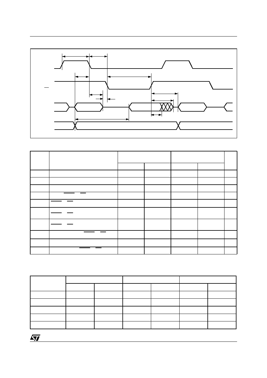
109/129
uPSD33XX
Figure 51. External PSEN/READ Cycle (80-pin Device Only)
Table 110. External PSEN or READ Cycle AC Characteristics (3V or 5V Device)
Note: 1. BUSCON Register is configured for 4 PFQCLK.
2. Refer to Table 111 for "n" and "m" values.
Table 111. n, m, and x, y Values
Symbol
Parameter
40MHz Oscillator
(1)
Variable Oscillator
1/t
CLCL
= 8 to 40MHz
Unit
Min
Max
Min
Max
t
LHLL
ALE pulse width
17
t
CLCL
≠ 8
ns
t
AVLL
Address setup to ALE
13
t
CLCL
≠ 12
ns
t
LLAX
Address hold after ALE
7.5
0.5t
CLCL
≠ 5
ns
t
LLPL
ALE to PSEN or RD
7.5
0.5t
CLCL
≠ 5
ns
t
PLPH
PSEN or RD pulse width
(2)
40
nt
CLCL
≠ 10
ns
t
PXIX
Input instruction/data hold after
PSEN or RD
2
2
ns
t
PHIZ
Input instruction/data float after
PSEN or RD
10.5
0.5t
CLCL
≠ 2
ns
t
PXAV
Address hold after PSEN or RD
7.5
0.5t
CLCL
≠ 5
ns
t
AVIV
Address to valid instruction/data in
(2)
70
mt
CLCL
≠ 5
ns
t
AZPL
Address float to PSEN or RD
≠2
≠2
ns
# of PFQCLK in
BUSCON Reg.
PSEN (code) Cycle
READ Cycle
WRITE Cycle
n
m
n
m
x
y
3
1
2
-
-
-
-
4
2
3
2
3
2
1
5
3
4
3
4
3
2
6
4
5
4
5
4
3
7
-
-
5
6
5
4
tAVLL
tPLPH
tPXIZ
tAVIV
PSEN
MCU
AD0 - AD7
MCU
A8 - A11
AI07875
tLHLL
ALE
RD
tLLPL
A0-A7
tLLAX
tAZPL
A0-A7
tPXAV
tPXIX
A8-A11
INSTR
IN
A8-A11

uPSD33XX
110/129
Figure 52. External WRITE Cycle (80-pin Device Only)
Table 112. External WRITE Cycle AC Characteristics (3V or 5V Device)
Note: 1. BUSCON Register is configured for 4 PFQCLK.
2. Refer to Table 111, page 109 for "n" and "m" values.
Table 113. External Clock Drive
Symbol
Parameter
40MHz Oscillator
(1)
Variable Oscillator
1/t
CLCL
= 8 to 40MHz
Unit
Min
Max
Min
Max
t
LHLL
ALE pulse width
17
t
CLCL
≠ 8
ns
t
AVLL
Address Setup to ALE
13
t
CLCL
≠ 12
ns
t
LLAX
Address hold after ALE
7.5
0.5t
CLCL
≠ 5
ns
t
WLWH
WR pulse width
(2)
40
xt
CLCL
≠ 10
ns
t
LLWL
ALE to WR
7.5
0.5t
CLCL
≠ 5
ns
t
AVWL
Address valid to WR
27.5
1.5t
CLCL
≠ 10
ns
t
WHLH
WR High to ALE High
6.5
14.5
0.5t
CLCL
≠ 6
0.5t
CLCL
+ 2
ns
t
QVWH
Data setup before WR
(y)
20
yt
CLCL
≠ 5
ns
t
WHQX
Data hold after WR
6.5
14.5
0.5t
CLCL
≠ 6
0.5t
CLCL
+ 2
ns
Symbol
Parameter
(1)
40MHz Oscillator
Variable Oscillator
1/t
CLCL
= 8 to 40MHz
Unit
Min
Max
Min
Max
t
CLCL
Oscillator period
25
125
ns
t
CHCX
High time
10
t
CLCL
≠ t
CLCX
ns
t
CLCX
Low time
10
t
CLCL
≠ t
CLCX
ns
t
CLCH
Rise time
10
ns
t
CHCL
Fall time
10
ns
MCU
A8 - A11
MCU
AD0 - AD7
ALE
WR
PSEN
A8-A11
A8-A11
tLLWL
tWLWH
tAVLL
tLHLL
tQVWH
DATA OUT
A0-A7
INSTR IN
A0-A7
tLLAX
tAVWL
tWHQX
tWHLH
AI07877

111/129
uPSD33XX
Table 114. A/D Analog Specification
Note: 1. f
IN
2kHz, ACLK = 8MHz, AV
REF
= V
CC
= 3.3V
2. AV
REF
= V
CC
in 52-pin package.
Symbol
Parameter
Test Conditions
(1)
Min.
Typ.
Max.
Unit
I
DD
Normal
Input = AV
REF
4.0
mA
Power-down
40
uA
AV
IN
Analog Input Voltage
GND
AV
REF
V
AV
REF
(2)
Analog Reference Voltage
3.6
V
Accuracy
Resolution
10
bits
INL
Integral Nonlinearity
Input = 0 ≠ AV
REF
(V)
±1
LSB
DNL
Differential Nonlinearity
Input = 0 ≠ AV
REF
(V)
±1
LSB
SNR
Signal to Noise Ratio
f
SAMPLE
= 500ksps
50
54
dB
SNDR
Signal to Noise Distortion Ratio
48
52
dB
ACLK
ADC Clock
2
8
16
MHz
t
C
Conversion Time
8MHz
1
4
8
µs
t
CAL
Power-up Time
Calibration Time
16
ms
f
IN
Analog Input Frequency
60
kHz
THD
Total Harmonic Distortion
50
54
dB

uPSD33XX
112/129
Figure 53. Input to Output Disable / Enable
Table 115. CPLD Combinatorial Timing (5V PSD Module)
Note: 1. Fast Slew Rate output available on PA3-PA0, PB3-PB0, and PD2-PD1. Decrement times by given amount
2. t
PD
for MCU address and control signals refers to delay from pins on Port 0, Port 2, RD WR, PSEN and ALE to CPLD combinatorial
output (80-pin package only)
Table 116. CPLD Combinatorial Timing (3V PSD Module)
Note: 1. Fast Slew Rate output available on PA3-PA0, PB3-PB0, and PD2-PD1. Decrement times by given amount
2. t
PD
for MCU address and control signals refers to delay from pins on Port 0, Port 2, RD WR, PSEN and ALE to CPLD combinatorial
output (80-pin package only)
Symbol
Parameter
Conditions
Min
Max
PT
Aloc
Turbo
Off
Slew
rate
(1)
Unit
t
PD
(2)
CPLD Input Pin/Feedback to
CPLD Combinatorial Output
20
+ 2
+ 10
≠ 2
ns
t
EA
CPLD Input to CPLD Output
Enable
21
+ 10
≠ 2
ns
t
ER
CPLD Input to CPLD Output
Disable
21
+ 10
≠ 2
ns
t
ARP
CPLD Register Clear or Preset
Delay
21
+ 10
≠ 2
ns
t
ARPW
CPLD Register Clear or Preset
Pulse Width
10
+ 10
ns
t
ARD
CPLD Array Delay
Any
macrocell
11
+ 2
ns
Symbol
Parameter
Conditions
Min
Max
PT
Aloc
Turbo
Off
Slew
rate
(1)
Unit
t
PD
(2)
CPLD Input Pin/Feedback to
CPLD Combinatorial Output
40
+ 4
+ 20
≠ 6
ns
t
EA
CPLD Input to CPLD Output
Enable
43
+ 20
≠ 6
ns
t
ER
CPLD Input to CPLD Output
Disable
43
+ 20
≠ 6
ns
t
ARP
CPLD Register Clear or
Preset Delay
40
+ 20
≠ 6
ns
t
ARPW
CPLD Register Clear or
Preset Pulse Width
25
+ 20
ns
t
ARD
CPLD Array Delay
Any
macrocell
25
+ 4
ns
tER
tEA
INPUT
INPUT TO
OUTPUT
ENABLE/DISABLE
AI02863

113/129
uPSD33XX
Figure 54. Synchronous Clock Mode Timing ≠ PLD
Table 117. CPLD Macrocell Synchronous Clock Mode Timing (5V PSD Module)
Note: 1. Fast Slew Rate output available on PA3-PA0, PB3-PB0, and PD2-PD1. Decrement times by given amount.
2. CLKIN (PD1) t
CLCL
= t
CH
+ t
CL
.
Table 118. CPLD Macrocell Synchronous Clock Mode Timing (3V PSD Module)
Note: 1. Fast Slew Rate output available on PA3-PA0, PB3-PB0, and PD2-PD1. Decrement times by given amount.
2. CLKIN (PD1) t
CLCL
= t
CH
+ t
CL
.
Symbol
Parameter
Conditions
Min
Max
PT
Aloc
Turbo
Off
Slew
rate
(1)
Unit
f
MAX
Maximum Frequency
External Feedback
1/(t
S
+t
CO
)
40.0
MHz
Maximum Frequency
Internal Feedback (f
CNT
)
1/(t
S
+t
CO
≠10)
66.6
MHz
Maximum Frequency
Pipelined Data
1/(t
CH
+t
CL
)
83.3
MHz
t
S
Input Setup Time
12
+ 2
+ 10
ns
t
H
Input Hold Time
0
ns
t
CH
Clock High Time
Clock Input
6
ns
t
CL
Clock Low Time
Clock Input
6
ns
t
CO
Clock to Output Delay
Clock Input
13
≠ 2
ns
t
ARD
CPLD Array Delay
Any macrocell
11
+ 2
ns
t
MIN
Minimum Clock Period
(2)
t
CH
+t
CL
12
ns
Symbol
Parameter
Conditions
Min
Max
PT
Aloc
Turbo
Off
Slew
rate
(1)
Unit
f
MAX
Maximum Frequency
External Feedback
1/(t
S
+t
CO
)
22.2
MHz
Maximum Frequency
Internal Feedback (f
CNT
)
1/(t
S
+t
CO
≠10)
28.5
MHz
Maximum Frequency
Pipelined Data
1/(t
CH
+t
CL
)
40.0
MHz
t
S
Input Setup Time
20
+ 4
+ 20
ns
t
H
Input Hold Time
0
ns
t
CH
Clock High Time
Clock Input
15
ns
t
CL
Clock Low Time
Clock Input
10
ns
t
CO
Clock to Output Delay
Clock Input
25
≠ 6
ns
t
ARD
CPLD Array Delay
Any macrocell
25
+ 4
ns
t
MIN
Minimum Clock Period
(2)
t
CH
+t
CL
25
ns
tCH
tCL
tCO
tH
tS
CLKIN
INPUT
REGISTERED
OUTPUT
AI02860

uPSD33XX
114/129
Figure 55. Asynchronous RESET / Preset
Figure 56. Asynchronous Clock Mode Timing (product term clock)
Table 119. CPLD Macrocell Asynchronous Clock Mode Timing (5V PSD Module)
Symbol
Parameter
Conditions
Min
Max
PT
Aloc
Turbo
Off
Slew
Rate
Unit
f
MAXA
Maximum Frequency
External Feedback
1/(t
SA
+t
COA
)
38.4
MHz
Maximum Frequency
Internal Feedback (f
CNTA
)
1/(t
SA
+t
COA
≠10)
62.5
MHz
Maximum Frequency
Pipelined Data
1/(t
CHA
+t
CLA
)
71.4
MHz
t
SA
Input Setup Time
7
+ 2
+ 10
ns
t
HA
Input Hold Time
8
ns
t
CHA
Clock Input High Time
9
+ 10
ns
t
CLA
Clock Input Low Time
9
+ 10
ns
t
COA
Clock to Output Delay
21
+ 10
≠ 2
ns
t
ARDA
CPLD Array Delay
Any macrocell
11
+ 2
ns
t
MINA
Minimum Clock Period
1/f
CNTA
16
ns
tARP
REGISTER
OUTPUT
tARPW
RESET/PRESET
INPUT
AI02864
tCHA
tCLA
tCOA
tHA
tSA
CLOCK
INPUT
REGISTERED
OUTPUT
AI02859

115/129
uPSD33XX
Table 120. CPLD Macrocell Asynchronous Clock Mode Timing (3V PSD Module)
Figure 57. Input Macrocell Timing (Product Term Clock)
Table 121. Input Macrocell Timing (5V PSD Module)
Note: 1. Inputs from Port A, B, and C relative to register/ latch clock from the PLD. ALE/AS latch timings refer to t
AVLX
and t
LXAX
.
Symbol
Parameter
Conditions
Min
Max
PT
Aloc
Turbo
Off
Slew
Rate
Unit
f
MAXA
Maximum Frequency
External Feedback
1/(t
SA
+t
COA
)
21.7
MHz
Maximum Frequency
Internal Feedback (f
CNTA
)
1/(t
SA
+t
COA
≠10)
27.8
MHz
Maximum Frequency
Pipelined Data
1/(t
CHA
+t
CLA
)
33.3
MHz
t
SA
Input Setup Time
10
+ 4
+ 20
ns
t
HA
Input Hold Time
12
ns
t
CHA
Clock High Time
17
+ 20
ns
t
CLA
Clock Low Time
13
+ 20
ns
t
COA
Clock to Output Delay
36
+ 20
≠ 6
ns
t
ARD
CPLD Array Delay
Any macrocell
25
+ 4
ns
t
MINA
Minimum Clock Period
1/f
CNTA
36
ns
Symbol
Parameter
Conditions
Min
Max
PT
Aloc
Turbo
Off
Unit
t
IS
Input Setup Time
(Note
1)
0
ns
t
IH
Input Hold Time
(Note
1)
15
+ 10
ns
t
INH
NIB Input High Time
(Note
1)
9
ns
t
INL
NIB Input Low Time
(Note
1)
9
ns
t
INO
NIB Input to Combinatorial Delay
(Note
1)
34
+ 2
+ 10
ns
t
INH
t
INL
t
INO
t
IH
t
IS
PT CLOCK
INPUT
OUTPUT
AI03101

uPSD33XX
116/129
Table 122. Input Macrocell Timing (3V PSD Module)
Note: 1. Inputs from Port A, B, and C relative to register/latch clock from the PLD. ALE latch timings refer to t
AVLX
and t
LXAX
.
Table 123. Program, WRITE and Erase Times (5V, 3V PSD Modules)
Note: 1. Programmed to all zero before erase.
2. The polling status, DQ7, is valid t
Q7VQV
time units before the data byte, DQ0-DQ7, is valid for reading.
Symbol
Parameter
Conditions
Min
Max
PT
Aloc
Turbo
Off
Unit
t
IS
Input Setup Time
(Note
1)
0
ns
t
IH
Input Hold Time
(Note
1)
25
+ 20
ns
t
INH
NIB Input High Time
(Note
1)
12
ns
t
INL
NIB Input Low Time
(Note
1)
12
ns
t
INO
NIB Input to Combinatorial Delay
(Note
1)
46
+ 4
+ 20
ns
Symbol
Parameter
Min.
Typ.
Max.
Unit
Flash Program
8.5
s
Flash Bulk Erase
(1)
(pre-programmed)
3
30
s
Flash Bulk Erase (not pre-programmed)
5
s
t
WHQV3
Sector Erase (pre-programmed)
1
30
s
t
WHQV2
Sector Erase (not pre-programmed)
2.2
s
t
WHQV1
Byte Program
14
150
µs
Program / Erase Cycles (per Sector)
100,000
cycles
t
WHWLO
Sector Erase Time-Out
100
µs
t
Q7VQV
DQ7 Valid to Output (DQ7-DQ0) Valid (Data Polling)
(2)
30
ns

117/129
uPSD33XX
Figure 58. Peripheral I/O READ Timing
Table 124. Port A Peripheral Data Mode READ Timing (5V PSD Module)
Note: 1. Any input used to select Port A Data Peripheral Mode.
2. Data is already stable on Port A.
Table 125. Port A Peripheral Data Mode READ Timing (3V PSD Module)
Note: 1. Any input used to select Port A Data Peripheral Mode.
2. Data is already stable on Port A.
Symbol
Parameter
Conditions
Min
Max
Turbo
Off
Unit
t
AVQV≠PA
Address Valid to Data
Valid
(Note
1)
37
+ 10
ns
t
SLQV≠PA
CSI Valid to Data Valid
27
+ 10
ns
t
RLQV≠PA
RD to Data Valid
(Note
2)
32
ns
t
DVQV≠PA
Data In to Data Out Valid
22
ns
t
RHQZ≠PA
RD to Data High-Z
23
ns
Symbol
Parameter
Conditions
Min
Max
Turbo
Off
Unit
t
AVQV≠PA
Address Valid to Data Valid
(Note
1)
50
+ 20
ns
t
SLQV≠PA
CSI Valid to Data Valid
37
+ 20
ns
t
RLQV≠PA
RD to Data Valid
(Note
2)
45
ns
t
DVQV≠PA
Data In to Data Out Valid
38
ns
t
RHQZ≠PA
RD to Data High-Z
36
ns
tRLQV (PA)
tDVQV (PA)
tRHQZ (PA)
tSLQV (PA)
tAVQV (PA)
ADDRESS
DATA VALID
ALE
A /D BUS
RD
DATA ON PORT A
CSI
AI06610
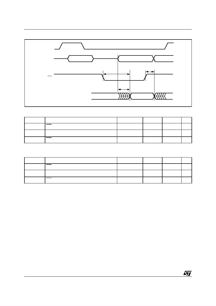
uPSD33XX
118/129
Figure 59. Peripheral I/O WRITE Timing
Table 126. Port A Peripheral Data Mode WRITE Timing (5V PSD Module)
Note: 1. Data stable on Port 0 pins to data on Port A.
Table 127. Port A Peripheral Data Mode WRITE Timing (3V PSD Module)
Note: 1. Data stable on Port 0 pins to data on Port A.
Symbol
Parameter
Conditions
Min
Max
Unit
t
WLQV≠PA
WR to Data Propagation Delay
25
ns
t
DVQV≠PA
Data to Port A Data Propagation Delay
(Note
1)
22
ns
t
WHQZ≠PA
WR Invalid to Port A Tri-state
20
ns
Symbol
Parameter
Conditions
Min
Max
Unit
t
WLQV≠PA
WR to Data Propagation Delay
42
ns
t
DVQV≠PA
Data to Port A Data Propagation Delay
(Note
1)
38
ns
t
WHQZ≠PA
WR Invalid to Port A Tri-state
33
ns
tDVQV (PA)
tWLQV (PA)
tWHQZ (PA)
ADDRESS
DATA OUT
A / D BUS
WR
PORT A
DATA OUT
ALE
AI06611

119/129
uPSD33XX
Figure 60. Reset (RESET) Timing
Table 128. Reset (RESET) Timing (5V PSD Module)
Note: 1. Reset (RESET) does not reset Flash memory Program or Erase cycles.
2. Warm RESET aborts Flash memory Program or Erase cycles, and puts the device in READ Mode.
Table 129. Reset (RESET) Timing (3V PSD Module)
Note: 1. Reset (RESET) does not reset Flash memory Program or Erase cycles.
2. Warm RESET aborts Flash memory Program or Erase cycles, and puts the device in READ Mode.
Table 130. V
STBYON
Definitions Timing (5V, 3V PSD Modules)
Note: 1. V
STBYON
timing is measured at V
CC
ramp rate of 2ms.
Symbol
Parameter
Conditions
Min
Max
Unit
t
NLNH
RESET Active Low Time
(1)
150
ns
t
NLNH≠PO
Power-on Reset Active Low Time
1
ms
t
NLNH≠A
Warm RESET
(2)
25
µ
s
t
OPR
RESET High to Operational Device
120
ns
Symbol
Parameter
Conditions
Min
Max
Unit
t
NLNH
RESET Active Low Time
(1)
300
ns
t
NLNH≠PO
Power-on Reset Active Low Time
1
ms
t
NLNH≠A
Warm RESET
(2)
25
µ
s
t
OPR
RESET High to Operational Device
300
ns
Symbol
Parameter
Conditions
Min
Typ
Max
Unit
t
BVBH
V
STBY
Detection to V
STBYON
Output High
(Note
1)
20
µs
t
BXBL
V
STBY
Off Detection to V
STBYON
Output
Low
(Note
1)
20
µs
tNLNH-PO
AI07874
RESET
tNLNH
tNLNH-A
V
CC
V
CC
(min)
Power-On Reset
Warm Reset

uPSD33XX
120/129
Figure 61. ISC Timing
Table 131. ISC Timing (5V PSD Module)
Note: 1. For non-PLD Programming, Erase or in ISC By-pass Mode.
2. For Program or Erase PLD only.
Symbol
Parameter
Conditions
Min
Max
Unit
t
ISCCF
Clock (TCK, PC1) Frequency (except for PLD)
(Note
1)
20
MHz
t
ISCCH
Clock (TCK, PC1) High Time (except for PLD)
(Note
1)
23
ns
t
ISCCL
Clock (TCK, PC1) Low Time (except for PLD)
(Note
1)
23
ns
t
ISCCFP
Clock (TCK, PC1) Frequency (PLD only)
(Note
2)
2
MHz
t
ISCCHP
Clock (TCK, PC1) High Time (PLD only)
(Note
2)
240
ns
t
ISCCLP
Clock (TCK, PC1) Low Time (PLD only)
(Note
2)
240
ns
t
ISCPSU
ISC Port Set Up Time
7
ns
t
ISCPH
ISC Port Hold Up Time
5
ns
t
ISCPCO
ISC Port Clock to Output
21
ns
t
ISCPZV
ISC Port High-Impedance to Valid Output
21
ns
t
ISCPVZ
ISC Port Valid Output to High-Impedance
21
ns
ISCCH
TCK
TDI/TMS
ISC OUTPUTS/TDO
ISC OUTPUTS/TDO
t
ISCCL
t
ISCPH
t
ISCPSU
t
ISCPVZ
t
ISCPZV
t
ISCPCO
t
AI02865

121/129
uPSD33XX
Table 132. ISC Timing (3V PSD Module)
Note: 1. For non-PLD Programming, Erase or in ISC By-pass Mode.
2. For Program or Erase PLD only.
Figure 62. MCU Module AC Measurement I/O Waveform
Note: AC inputs during testing are driven at V
CC
≠0.5V for a logic '1,' and 0.45V for a logic '0.'
Timing measurements are made at V
IH
(min) for a logic '1,' and V
IL
(max) for a logic '0'
Figure 63. PSD Module AC Float I/O Waveform
Note: For timing purposes, a Port pin is considered to be no longer floating when a 100mV change from load voltage occurs, and begins to
float when a 100mV change from the loaded V
OH
or V
OL
level occurs
I
OL
and I
OH
20mA
Symbol
Parameter
Conditions
Min
Max
Unit
t
ISCCF
Clock (TCK, PC1) Frequency (except for PLD)
(Note
1)
12
MHz
t
ISCCH
Clock (TCK, PC1) High Time (except for PLD)
(Note
1)
40
ns
t
ISCCL
Clock (TCK, PC1) Low Time (except for PLD)
(Note
1)
40
ns
t
ISCCFP
Clock (TCK, PC1) Frequency (PLD only)
(Note
2)
2
MHz
t
ISCCHP
Clock (TCK, PC1) High Time (PLD only)
(Note
2)
240
ns
t
ISCCLP
Clock (TCK, PC1) Low Time (PLD only)
(Note
2)
240
ns
t
ISCPSU
ISC Port Set Up Time
12
ns
t
ISCPH
ISC Port Hold Up Time
5
ns
t
ISCPCO
ISC Port Clock to Output
30
ns
t
ISCPZV
ISC Port High-Impedance to Valid Output
30
ns
t
ISCPVZ
ISC Port Valid Output to High-Impedance
30
ns
AI06650
VCC ≠ 0.5V
0.45V
Test Points
0.2 VCC ≠ 0.1V
0.2 VCC + 0.9V
AI06651
Test Reference Points
VOL + 0.1V
VOH ≠ 0.1V
VLOAD ≠ 0.1V
VLOAD + 0.1V
0.2 VCC ≠ 0.1V

uPSD33XX
122/129
Figure 64. External Clock Cycle
Figure 65. Recommended Oscillator Circuits
Note: C1, C2 = 30pF ± 10pF for crystals
For ceramic resonators, contact resonator manufacturer
Oscillation circuit is designed to be used either with a ceramic resonator or crystal oscillator. Since each crystal and ceramic resonator
have their own characteristics, the user should consult the crystal manufacturer for appropriate values of external components.
Figure 66. PSD Module AC Measurement I/O
Waveform
Figure 67. PSD Module AC Measurement Load
Circuit
Table 133. I/O Pin Capacitance
Note: 1. Sampled only, not 100% tested.
2. Typical values are for T
A
= 25∞C and nominal supply voltages.
3.0V
0V
Test Point
1.5V
AI03103b
Device
Under Test
2.01 V
195
C
L
= 30 pF
(Including Scope and
Jig Capacitance)
AI03104b
Symbol
Parameter
Test Condition
Typ.
2
Max
.
Unit
C
IN
Input Capacitance (for input pins)
V
IN
= 0V
4
6
pF
C
OUT
Output Capacitance (for input/
output pins)
V
OUT
= 0V
8
12
pF

123/129
uPSD33XX
PART NUMBERING
Table 134. Ordering Information Scheme
For a list of available options (e.g., Speed, Package) or for further information on any aspect of this device,
please contact the ST Sales Office nearest to you.
Example:
UPSD
33
3
4
D
V
≠
24
U
6
T
Device Type
uPSD = Microcontroller PSD
Family
33 = Turbo core
SRAM Size
1 = 16Kbit
3 = 64Kbit
5 = 256Kbit
Main Flash Memory Size
2 = 512Kbit
3 = 1Mbit
4 = 2Mbit
IP Mix
D = IP Mix: I
2
C, SPI, UART (2), IrDA, ADC, Supervisor, PCA
Operating Voltage
blank = V
CC
= 4.5 to 5.5V
V = V
CC
= 3.0 to 3.6V
Speed
≠24 = 24MHz
≠40 = 40MHz
Package
T = 52-pin TQFP
U = 80-pin TQFP
Temperature Range
1 = 0 to 70∞C
6 = ≠40 to 85∞C
Shipping Option
Tape & Reel Packing = T

uPSD33XX
124/129
PACKAGE MECHANICAL INFORMATION
Figure 68. TQFP52 ≠ 52-lead Plastic Quad Flatpack Package Outline
Note: Drawing is not to scale.
QFP-A
Nd
E1
CP
b
e
A2
A
N
L
A1
D1
D
1
E
Ne
c
D2
E2
L1

125/129
uPSD33XX
Table 135. TQFP52 ≠ 52-lead Plastic Quad Flatpack Package Mechanical Data
Symb
mm
inches
Typ
Min
Max
Typ
Min
Max
A
≠
≠
1.75
≠
≠
0.069
A1
≠
0.05
0.20
≠
0.002
0.008
A2
≠
1.25
1.55
≠
0.049
0.061
b
≠
0.20
0.40
≠
0.008
0.016
c
≠
0.07
0.23
≠
0.002
0.009
D
12.00
≠
≠
0.473
≠
≠
D1
10.00
≠
≠
0.394
≠
≠
D2
E
12.00
≠
≠
0.473
≠
≠
E1
10.00
≠
≠
0.394
≠
≠
E2
7.80
0.307
e
0.65
≠
≠
0.026
≠
≠
L
≠
0.45
0.75
≠
0.018
0.030
L1
1.00
≠
≠
0.039
≠
≠
≠
0∞
7∞
≠
0∞
7∞
n
52
52
Nd
13
13
Ne
13
13
CP
≠
≠
0.10
≠
≠
0.004

uPSD33XX
126/129
Figure 69. TQFP80 ≠ 80-lead Plastic Quad Flatpack Package Outline
Note: Drawing is not to scale.
QFP-A
Nd
E1
CP
b
e
A2
A
N
L
A1
D1
D
1
E
Ne
c
D2
E2
L1

127/129
uPSD33XX
Table 136. TQFP80 ≠ 80-lead Plastic Quad Flatpack Package Mechanical Data
Symb
mm
inches
Typ
Min
Max
Typ
Min
Max
A
≠
≠
1.60
≠
≠
0.063
A1
≠
0.05
0.15
≠
0.002
0.006
A2
1.40
1.35
1.45
0.055
0.053
0.057
b
0.22
0.17
0.27
0.009
0.007
0.011
c
≠
0.09
0.20
≠
0.004
0.008
D
14.00
≠
≠
0.551
≠
≠
D1
12.00
≠
≠
0.472
≠
≠
D2
9.50
≠
≠
0.374
≠
≠
E
14.00
≠
≠
0.473
≠
≠
E1
12.00
≠
≠
0.394
≠
≠
E2
9.50
≠
≠
0.374
≠
≠
e
0.50
≠
≠
0.020
≠
≠
L
0.60
0.45
0.75
0.024
0.018
0.030
L1
1.00
≠
≠
0.039
≠
≠
3.5
0∞
7∞
3.5
0∞
7∞
n
80
80
Nd
20
20
Ne
20
20
CP
≠
≠
0.08
≠
≠
0.003

uPSD33XX
128/129
REVISION HISTORY
Table 137. Document Revision History
Date
Rev. #
Revision Details
July 2003
1.0
First Issue
15-Jul-03
1.1
Update register information, electrical characteristics (Table 17, 46, 110, 111, 112, 113;
Figure 51)
03-Sep-03
1.2
Update references for Product Catalog

129/129
uPSD33XX
Information furnished is believed to be accurate and reliable. However, STMicroelectronics assumes no responsibility for the consequences
of use of such information nor for any infringement of patents or other rights of third parties which may result from its use. No license is granted
by implication or otherwise under any patent or patent rights of STMicroelectronics. Specifications mentioned in this publication are subject
to change without notice. This publication supersedes and replaces all information previously supplied. STMicroelectronics products are not
authorized for use as critical components in life support devices or systems without express written approval of STMicroelectronics.
The ST logo is a registered trademark of STMicroelectronics.
All other names are the property of their respective owners
© 2003 STMicroelectronics - All rights reserved
STMicroelectronics GROUP OF COMPANIES
Australia - Belgium - Brazil - Canada - China - Czech Republic - Finland - France - Germany - Hong Kong - India - Israel - Italy - Japan -
Malaysia - Malta - Morocco - Singapore - Spain - Sweden - Switzerland - United Kingdom - United States
www.st.com