 | –≠–ª–µ–∫—Ç—Ä–æ–Ω–Ω—ã–π –∫–æ–º–ø–æ–Ω–µ–Ω—Ç: UPSD3432 | –°–∫–∞—á–∞—Ç—å:  PDF PDF  ZIP ZIP |
1/264
PRELIMINARY DATA
March 2005
This is preliminary information on a new product now in development or undergoing evaluation. Details are subject to change without notice.
uPSD34xx
Turbo Plus Series
Fast Turbo 8032 MCU with USB and Programmable Logic
Rev 2.0
FEATURES SUMMARY
FAST 8-BIT TURBO 8032 MCU, 40MHz
≠
Advanced core, 4-clocks per instruction
≠
10 MIPs peak performance at 40MHz (5V)
≠
JTAG Debug and In-System
Programming
≠
16-bit internal instruction path fetches
double-byte instruction in a single memory
cycle
≠
Branch Cache & 4 instruction Prefetch
Queue
≠
Dual XDATA pointers with automatic
increment and decrement
≠
Compatible with 3rd party 8051 tools
DUAL FLASH MEMORIES WITH MEMORY
MANAGEMENT
≠
Place either memory into 8032 program
address space or data address space
≠
READ-while-WRITE operation for In-
Application Programming and EEPROM
emulation
≠
Single voltage program and erase
≠
100K guaranteed erase cycles, 15-year
retention
CLOCK, RESET, AND POWER SUPPLY
MANAGEMENT
≠
SRAM is Battery Backup capable
≠
Flexible 8-level CPU clock divider register
≠
Normal, Idle, and Power Down Modes
≠
Power-on and Low Voltage reset
supervisor
≠
Programmable Watchdog Timer
PROGRAMMABLE LOGIC, GENERAL
PURPOSE
≠
16 macrocells for logic applications (e.g.,
shifters, state machines, chip-selects,
glue-logic to keypads, and LCDs)
A/D CONVERTER
≠
Eight Channels, 10-bit resolution, 6µs
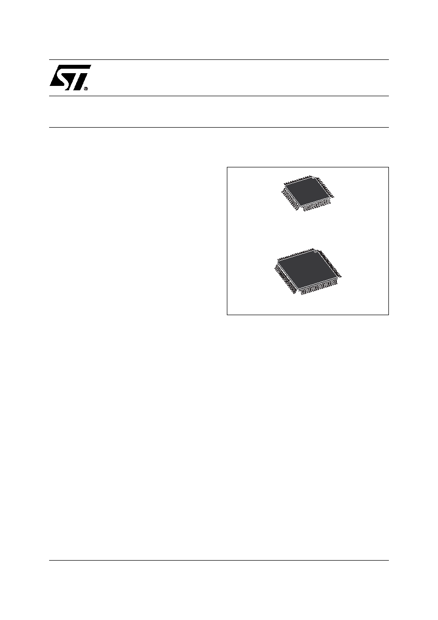
Figure 1. Packages
COMMUNICATION INTERFACES
≠
USB v2.0 Full Speed (12Mbps)
10 endpoint pairs (In/Out), each endpoint
with 64-byte FIFO (supports Control, Intr,
and Bulk transfer types)
≠
I
2
C Master/Slave controller, 833kHz
≠
SPI Master controller, 1MHz
≠
Two UARTs with independent baud rate
≠
IrDA Potocol: up to 115 kbaud
≠
Up to 46 I/O, 5V tolerant uPSD34xxV
TIMERS AND INTERRUPTS
≠
Three 8032 standard 16-bit timers
≠
Programmable Counter Array (PCA), six
16-bit modules for PWM, CAPCOM, and
timers
≠
8/10/16-bit PWM operation
≠
12 Interrupt sources with two external
interrupt pins
OPERATING VOLTAGE SOURCE (±10%)
≠
5V Devices: 5.0V and 3.3V sources
≠
3.3V Devices: 3.3V source
TQFP52 (T), 52-lead, Thin, Quad, Flat
TQFP80 (U), 80-lead, Thin, Quad, Flat

uPSD34xx - FEATURES SUMMARY
2/264
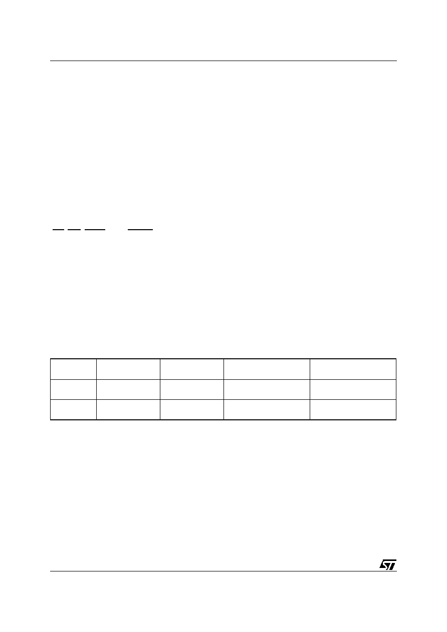
Table 1. Device Summary
Note: Operating temperature is in the Industrial range (≠40∞C to 85∞C).
Part Number
Max MHz
1st
Flash
(bytes)
2nd
Flash
SRAM
GPIO
8032
Bus
V
CC
V
DD
Pkg.
uPSD3422E-40T6
40
64K
32K
4K
35
No
3.3V
5.0V
TQFP52
uPSD3422EV-40T6
40
64K
32K
4K
35
No
3.3V
3.3V
TQFP52
uPSD3422E-40U6
40
64K
32K
4K
46
Yes
3.3V
5.0V
TQFP80
uPSD3422EV-40U6
40
64K
32K
4K
46
Yes
3.3V
3.3V
TQFP80
uPSD3433E-40T6
40
128K
32K
8K
35
No
3.3V
5.0V
TQFP52
uPSD3433EV-40T6
40
128K
32K
8K
35
No
3.3V
3.3V
TQFP52
uPSD3433E-40U6
40
128K
32K
8K
46
Yes
3.3V
5.0V
TQFP80
uPSD3433EV-40U6
40
128K
32K
8K
46
Yes
3.3V
3.3V
TQFP80
uPSD3434E-40T6
40
256K
32K
8K
35
No
3.3V
5.0V
TQFP52
uPSD3434EV-40T6
40
256K
32K
8K
35
No
3.3V
3.3V
TQFP52
uPSD3434E-40U6
40
256K
32K
8K
46
Yes
3.3V
5.0V
TQFP80
uPSD3434EV-40U6
40
256K
32K
8K
46
Yes
3.3V
3.3V
TQFP80

3/264
uPSD34xx - TABLE OF CONTENTS
TABLE OF CONTENTS
FEATURES SUMMARY . . . . . . . . . . . . . . . . . . . . . . . . . . . . . . . . . . . . . . . . . . . . . . . . . . . . . . . . . . . . . 1
TABLE OF CONTENTS . . . . . . . . . . . . . . . . . . . . . . . . . . . . . . . . . . . . . . . . . . . . . . . . . . . . . . . . . . . . . 3
SUMMARY DESCRIPTION . . . . . . . . . . . . . . . . . . . . . . . . . . . . . . . . . . . . . . . . . . . . . . . . . . . . . . . . . . . 7
PIN DESCRIPTIONS . . . . . . . . . . . . . . . . . . . . . . . . . . . . . . . . . . . . . . . . . . . . . . . . . . . . . . . . . . . . . . . . 9
HARDWARE DESCRIPTION . . . . . . . . . . . . . . . . . . . . . . . . . . . . . . . . . . . . . . . . . . . . . . . . . . . . . . . . 14
MEMORY ORGANIZATION . . . . . . . . . . . . . . . . . . . . . . . . . . . . . . . . . . . . . . . . . . . . . . . . . . . . . . . . . 16
Internal Memory (MCU Module, Standard 8032 Memory: DATA, IDATA, SFR) . . . . . . . . . . . . 17
External Memory (PSD Module: Program memory, Data memory). . . . . . . . . . . . . . . . . . . . . . 17
8032 MCU CORE PERFORMANCE ENHANCEMENTS . . . . . . . . . . . . . . . . . . . . . . . . . . . . . . . . . . . 18
Pre-Fetch Queue (PFQ) and Branch Cache (BC) . . . . . . . . . . . . . . . . . . . . . . . . . . . . . . . . . . . . 20
PFQ Example, Multi-cycle Instructions . . . . . . . . . . . . . . . . . . . . . . . . . . . . . . . . . . . . . . . . . . . . 20
Aggregate Performance . . . . . . . . . . . . . . . . . . . . . . . . . . . . . . . . . . . . . . . . . . . . . . . . . . . . . . . . 20
MCU MODULE DISCRIPTION . . . . . . . . . . . . . . . . . . . . . . . . . . . . . . . . . . . . . . . . . . . . . . . . . . . . . . . 22
8032 MCU REGISTERS . . . . . . . . . . . . . . . . . . . . . . . . . . . . . . . . . . . . . . . . . . . . . . . . . . . . . . . . . . . . 22
Stack Pointer (SP) . . . . . . . . . . . . . . . . . . . . . . . . . . . . . . . . . . . . . . . . . . . . . . . . . . . . . . . . . . . . . 22
Data Pointer (DPTR) . . . . . . . . . . . . . . . . . . . . . . . . . . . . . . . . . . . . . . . . . . . . . . . . . . . . . . . . . . . 22
Program Counter (PC). . . . . . . . . . . . . . . . . . . . . . . . . . . . . . . . . . . . . . . . . . . . . . . . . . . . . . . . . . 22
Accumulator (ACC) . . . . . . . . . . . . . . . . . . . . . . . . . . . . . . . . . . . . . . . . . . . . . . . . . . . . . . . . . . . . 22
B Register (B). . . . . . . . . . . . . . . . . . . . . . . . . . . . . . . . . . . . . . . . . . . . . . . . . . . . . . . . . . . . . . . . . 22
General Purpose Registers (R0 - R7). . . . . . . . . . . . . . . . . . . . . . . . . . . . . . . . . . . . . . . . . . . . . . 23
Program Status Word (PSW) . . . . . . . . . . . . . . . . . . . . . . . . . . . . . . . . . . . . . . . . . . . . . . . . . . . . 23
SPECIAL FUNCTION REGISTERS (SFR) . . . . . . . . . . . . . . . . . . . . . . . . . . . . . . . . . . . . . . . . . . . . . . 24
8032 ADDRESSING MODES . . . . . . . . . . . . . . . . . . . . . . . . . . . . . . . . . . . . . . . . . . . . . . . . . . . . . . . . 31
Register Addressing . . . . . . . . . . . . . . . . . . . . . . . . . . . . . . . . . . . . . . . . . . . . . . . . . . . . . . . . . . . 31
Direct Addressing . . . . . . . . . . . . . . . . . . . . . . . . . . . . . . . . . . . . . . . . . . . . . . . . . . . . . . . . . . . . . 31
Register Indirect Addressing . . . . . . . . . . . . . . . . . . . . . . . . . . . . . . . . . . . . . . . . . . . . . . . . . . . . 31
Immediate Addressing . . . . . . . . . . . . . . . . . . . . . . . . . . . . . . . . . . . . . . . . . . . . . . . . . . . . . . . . . 31
External Direct Addressing . . . . . . . . . . . . . . . . . . . . . . . . . . . . . . . . . . . . . . . . . . . . . . . . . . . . . 31
External Indirect Addressing . . . . . . . . . . . . . . . . . . . . . . . . . . . . . . . . . . . . . . . . . . . . . . . . . . . . 31
Indexed Addressing . . . . . . . . . . . . . . . . . . . . . . . . . . . . . . . . . . . . . . . . . . . . . . . . . . . . . . . . . . . 32
Relative Addressing . . . . . . . . . . . . . . . . . . . . . . . . . . . . . . . . . . . . . . . . . . . . . . . . . . . . . . . . . . . 32
Absolute Addressing . . . . . . . . . . . . . . . . . . . . . . . . . . . . . . . . . . . . . . . . . . . . . . . . . . . . . . . . . . 32
Long Addressing . . . . . . . . . . . . . . . . . . . . . . . . . . . . . . . . . . . . . . . . . . . . . . . . . . . . . . . . . . . . . . 32
Bit Addressing . . . . . . . . . . . . . . . . . . . . . . . . . . . . . . . . . . . . . . . . . . . . . . . . . . . . . . . . . . . . . . . . 32

uPSD34xx - TABLE OF CONTENTS
4/264
uPSD34xx INSTRUCTION SET SUMMARY . . . . . . . . . . . . . . . . . . . . . . . . . . . . . . . . . . . . . . . . . . . . 33
DUAL DATA POINTERS. . . . . . . . . . . . . . . . . . . . . . . . . . . . . . . . . . . . . . . . . . . . . . . . . . . . . . . . . . . . 38
Data Pointer Control Register, DPTC (85h) . . . . . . . . . . . . . . . . . . . . . . . . . . . . . . . . . . . . . . . . . 38
Data Pointer Mode Register, DPTM (86h) . . . . . . . . . . . . . . . . . . . . . . . . . . . . . . . . . . . . . . . . . . 39
DEBUG UNIT. . . . . . . . . . . . . . . . . . . . . . . . . . . . . . . . . . . . . . . . . . . . . . . . . . . . . . . . . . . . . . . . . . . . . 40
INTERRUPT SYSTEM. . . . . . . . . . . . . . . . . . . . . . . . . . . . . . . . . . . . . . . . . . . . . . . . . . . . . . . . . . . . . . 41
Individual Interrupt Sources . . . . . . . . . . . . . . . . . . . . . . . . . . . . . . . . . . . . . . . . . . . . . . . . . . . . . 44
MCU CLOCK GENERATION . . . . . . . . . . . . . . . . . . . . . . . . . . . . . . . . . . . . . . . . . . . . . . . . . . . . . . . . 47
MCU_CLK . . . . . . . . . . . . . . . . . . . . . . . . . . . . . . . . . . . . . . . . . . . . . . . . . . . . . . . . . . . . . . . . . . . . 47
PERIPH_CLK . . . . . . . . . . . . . . . . . . . . . . . . . . . . . . . . . . . . . . . . . . . . . . . . . . . . . . . . . . . . . . . . . 47
POWER SAVING MODES . . . . . . . . . . . . . . . . . . . . . . . . . . . . . . . . . . . . . . . . . . . . . . . . . . . . . . . . . . 50
Idle Mode . . . . . . . . . . . . . . . . . . . . . . . . . . . . . . . . . . . . . . . . . . . . . . . . . . . . . . . . . . . . . . . . . . . . 50
Power-down Mode . . . . . . . . . . . . . . . . . . . . . . . . . . . . . . . . . . . . . . . . . . . . . . . . . . . . . . . . . . . . . 50
Reduced Frequency Mode . . . . . . . . . . . . . . . . . . . . . . . . . . . . . . . . . . . . . . . . . . . . . . . . . . . . . . 50
OSCILLATOR AND EXTERNAL COMPONENTS . . . . . . . . . . . . . . . . . . . . . . . . . . . . . . . . . . . . . . . . 53
I/O PORTS of MCU MODULE. . . . . . . . . . . . . . . . . . . . . . . . . . . . . . . . . . . . . . . . . . . . . . . . . . . . . . . . 54
MCU Port Operating Modes . . . . . . . . . . . . . . . . . . . . . . . . . . . . . . . . . . . . . . . . . . . . . . . . . . . . . 54
MCU BUS INTERFACE. . . . . . . . . . . . . . . . . . . . . . . . . . . . . . . . . . . . . . . . . . . . . . . . . . . . . . . . . . . . . 63
PSEN Bus Cycles . . . . . . . . . . . . . . . . . . . . . . . . . . . . . . . . . . . . . . . . . . . . . . . . . . . . . . . . . . . . . 63
READ or WRITE Bus Cycles . . . . . . . . . . . . . . . . . . . . . . . . . . . . . . . . . . . . . . . . . . . . . . . . . . . . . 63
Connecting External Devices to the MCU Bus . . . . . . . . . . . . . . . . . . . . . . . . . . . . . . . . . . . . . . 63
Programmable Bus Timing . . . . . . . . . . . . . . . . . . . . . . . . . . . . . . . . . . . . . . . . . . . . . . . . . . . . . . 64
Controlling the PFQ and BC . . . . . . . . . . . . . . . . . . . . . . . . . . . . . . . . . . . . . . . . . . . . . . . . . . . . . 64
SUPERVISORY FUNCTIONS . . . . . . . . . . . . . . . . . . . . . . . . . . . . . . . . . . . . . . . . . . . . . . . . . . . . . . . . 67
External Reset Input Pin, RESET_IN . . . . . . . . . . . . . . . . . . . . . . . . . . . . . . . . . . . . . . . . . . . . . . 67
Low V
CC
Voltage Detect, LVD. . . . . . . . . . . . . . . . . . . . . . . . . . . . . . . . . . . . . . . . . . . . . . . . . . . . 68
Power-up Reset . . . . . . . . . . . . . . . . . . . . . . . . . . . . . . . . . . . . . . . . . . . . . . . . . . . . . . . . . . . . . . . 68
JTAG Debug Reset . . . . . . . . . . . . . . . . . . . . . . . . . . . . . . . . . . . . . . . . . . . . . . . . . . . . . . . . . . . . 68
Watchdog Timer, WDT . . . . . . . . . . . . . . . . . . . . . . . . . . . . . . . . . . . . . . . . . . . . . . . . . . . . . . . . . 68
STANDARD 8032 TIMER/COUNTERS . . . . . . . . . . . . . . . . . . . . . . . . . . . . . . . . . . . . . . . . . . . . . . . . 71
Standard Timer SFRs . . . . . . . . . . . . . . . . . . . . . . . . . . . . . . . . . . . . . . . . . . . . . . . . . . . . . . . . . . 71
Clock Sources . . . . . . . . . . . . . . . . . . . . . . . . . . . . . . . . . . . . . . . . . . . . . . . . . . . . . . . . . . . . . . . . 71
SFR, TCON . . . . . . . . . . . . . . . . . . . . . . . . . . . . . . . . . . . . . . . . . . . . . . . . . . . . . . . . . . . . . . . . . . . 73
SFR, TMOD . . . . . . . . . . . . . . . . . . . . . . . . . . . . . . . . . . . . . . . . . . . . . . . . . . . . . . . . . . . . . . . . . . . 73
Timer 0 and Timer 1 Operating Modes . . . . . . . . . . . . . . . . . . . . . . . . . . . . . . . . . . . . . . . . . . . . 73
Timer 2 . . . . . . . . . . . . . . . . . . . . . . . . . . . . . . . . . . . . . . . . . . . . . . . . . . . . . . . . . . . . . . . . . . . . . . 76

5/264
uPSD34xx - TABLE OF CONTENTS
SERIAL UART INTERFACES . . . . . . . . . . . . . . . . . . . . . . . . . . . . . . . . . . . . . . . . . . . . . . . . . . . . . . . . 83
UART Operation Modes . . . . . . . . . . . . . . . . . . . . . . . . . . . . . . . . . . . . . . . . . . . . . . . . . . . . . . . . 83
Serial Port Control Registers . . . . . . . . . . . . . . . . . . . . . . . . . . . . . . . . . . . . . . . . . . . . . . . . . . . . 84
UART Baud Rates . . . . . . . . . . . . . . . . . . . . . . . . . . . . . . . . . . . . . . . . . . . . . . . . . . . . . . . . . . . . . 86
More About UART Mode 0 . . . . . . . . . . . . . . . . . . . . . . . . . . . . . . . . . . . . . . . . . . . . . . . . . . . . . . 87
More About UART Mode 1 . . . . . . . . . . . . . . . . . . . . . . . . . . . . . . . . . . . . . . . . . . . . . . . . . . . . . . 89
More About UART Modes 2 and 3 . . . . . . . . . . . . . . . . . . . . . . . . . . . . . . . . . . . . . . . . . . . . . . . . 91
IrDA INTERFACE . . . . . . . . . . . . . . . . . . . . . . . . . . . . . . . . . . . . . . . . . . . . . . . . . . . . . . . . . . . . . . . . . 94
Baud Rate Selection . . . . . . . . . . . . . . . . . . . . . . . . . . . . . . . . . . . . . . . . . . . . . . . . . . . . . . . . . . . 95
Pulse Width Selection . . . . . . . . . . . . . . . . . . . . . . . . . . . . . . . . . . . . . . . . . . . . . . . . . . . . . . . . . . 97
I
2
C INTERFACE . . . . . . . . . . . . . . . . . . . . . . . . . . . . . . . . . . . . . . . . . . . . . . . . . . . . . . . . . . . . . . . . . . 98
I2C Interface Main Features . . . . . . . . . . . . . . . . . . . . . . . . . . . . . . . . . . . . . . . . . . . . . . . . . . . . . 98
Communication Flow . . . . . . . . . . . . . . . . . . . . . . . . . . . . . . . . . . . . . . . . . . . . . . . . . . . . . . . . . . 99
Operating Modes . . . . . . . . . . . . . . . . . . . . . . . . . . . . . . . . . . . . . . . . . . . . . . . . . . . . . . . . . . . . . 101
Bus Arbitration . . . . . . . . . . . . . . . . . . . . . . . . . . . . . . . . . . . . . . . . . . . . . . . . . . . . . . . . . . . . . . 101
Clock Synchronization . . . . . . . . . . . . . . . . . . . . . . . . . . . . . . . . . . . . . . . . . . . . . . . . . . . . . . . . 101
General Call Address . . . . . . . . . . . . . . . . . . . . . . . . . . . . . . . . . . . . . . . . . . . . . . . . . . . . . . . . . 101
Serial I/O Engine (SIOE) . . . . . . . . . . . . . . . . . . . . . . . . . . . . . . . . . . . . . . . . . . . . . . . . . . . . . . . 102
I
2
C Interface Control Register (S1CON) . . . . . . . . . . . . . . . . . . . . . . . . . . . . . . . . . . . . . . . . . . 103
I
2
C Interface Status Register (S1STA) . . . . . . . . . . . . . . . . . . . . . . . . . . . . . . . . . . . . . . . . . . . . 105
I2C Data Shift Register (S1DAT). . . . . . . . . . . . . . . . . . . . . . . . . . . . . . . . . . . . . . . . . . . . . . . . . 107
I
2
C Address Register (S1ADR) . . . . . . . . . . . . . . . . . . . . . . . . . . . . . . . . . . . . . . . . . . . . . . . . . . 107
I
2
C START Sample Setting (S1SETUP) . . . . . . . . . . . . . . . . . . . . . . . . . . . . . . . . . . . . . . . . . . . 108
I
2
C Operating Sequences . . . . . . . . . . . . . . . . . . . . . . . . . . . . . . . . . . . . . . . . . . . . . . . . . . . . . . 111
SPI (SYNCHRONOUS PERIPHERAL INTERFACE) . . . . . . . . . . . . . . . . . . . . . . . . . . . . . . . . . . . . . 115
SPI Bus Features and Communication Flow . . . . . . . . . . . . . . . . . . . . . . . . . . . . . . . . . . . . . . 116
Full-Duplex Operation . . . . . . . . . . . . . . . . . . . . . . . . . . . . . . . . . . . . . . . . . . . . . . . . . . . . . . . . . 116
Bus-Level Activity . . . . . . . . . . . . . . . . . . . . . . . . . . . . . . . . . . . . . . . . . . . . . . . . . . . . . . . . . . . . 116
SPI SFR Registers . . . . . . . . . . . . . . . . . . . . . . . . . . . . . . . . . . . . . . . . . . . . . . . . . . . . . . . . . . . . 118
SPI Configuration . . . . . . . . . . . . . . . . . . . . . . . . . . . . . . . . . . . . . . . . . . . . . . . . . . . . . . . . . . . . 119
Dynamic Control . . . . . . . . . . . . . . . . . . . . . . . . . . . . . . . . . . . . . . . . . . . . . . . . . . . . . . . . . . . . . 119
USB INTERFACE . . . . . . . . . . . . . . . . . . . . . . . . . . . . . . . . . . . . . . . . . . . . . . . . . . . . . . . . . . . . . . . . 123
Basic USB Concepts . . . . . . . . . . . . . . . . . . . . . . . . . . . . . . . . . . . . . . . . . . . . . . . . . . . . . . . . . . 124
Types of Transfers . . . . . . . . . . . . . . . . . . . . . . . . . . . . . . . . . . . . . . . . . . . . . . . . . . . . . . . . . . . 127
Endpoint FIFOs . . . . . . . . . . . . . . . . . . . . . . . . . . . . . . . . . . . . . . . . . . . . . . . . . . . . . . . . . . . . . . 129
USB Registers . . . . . . . . . . . . . . . . . . . . . . . . . . . . . . . . . . . . . . . . . . . . . . . . . . . . . . . . . . . . . . . 132
Typical Connection to USB . . . . . . . . . . . . . . . . . . . . . . . . . . . . . . . . . . . . . . . . . . . . . . . . . . . . 150
ANALOG-TO-DIGITAL CONVERTOR (ADC) . . . . . . . . . . . . . . . . . . . . . . . . . . . . . . . . . . . . . . . . . . 151
Port 1 ADC Channel Selects . . . . . . . . . . . . . . . . . . . . . . . . . . . . . . . . . . . . . . . . . . . . . . . . . . . . 151

uPSD34xx - TABLE OF CONTENTS
6/264
PROGRAMMABLE COUNTER ARRAY (PCA) WITH PWM . . . . . . . . . . . . . . . . . . . . . . . . . . . . . . . 154
PCA Block . . . . . . . . . . . . . . . . . . . . . . . . . . . . . . . . . . . . . . . . . . . . . . . . . . . . . . . . . . . . . . . . . . 154
PCA Clock Selection . . . . . . . . . . . . . . . . . . . . . . . . . . . . . . . . . . . . . . . . . . . . . . . . . . . . . . . . . . 156
Operation of TCM Modes . . . . . . . . . . . . . . . . . . . . . . . . . . . . . . . . . . . . . . . . . . . . . . . . . . . . . . 157
Capture Mode. . . . . . . . . . . . . . . . . . . . . . . . . . . . . . . . . . . . . . . . . . . . . . . . . . . . . . . . . . . . . . . . 157
Timer Mode . . . . . . . . . . . . . . . . . . . . . . . . . . . . . . . . . . . . . . . . . . . . . . . . . . . . . . . . . . . . . . . . . 157
Toggle Mode . . . . . . . . . . . . . . . . . . . . . . . . . . . . . . . . . . . . . . . . . . . . . . . . . . . . . . . . . . . . . . . . 157
PWM Mode - (X8), Fixed Frequency . . . . . . . . . . . . . . . . . . . . . . . . . . . . . . . . . . . . . . . . . . . . . . 157
PWM Mode - (X8), Programmable Frequency . . . . . . . . . . . . . . . . . . . . . . . . . . . . . . . . . . . . . . 159
PWM Mode - Fixed Frequency, 16-bit . . . . . . . . . . . . . . . . . . . . . . . . . . . . . . . . . . . . . . . . . . . . 160
PWM Mode - Fixed Frequency, 10-bit . . . . . . . . . . . . . . . . . . . . . . . . . . . . . . . . . . . . . . . . . . . . 160
Writing to Capture/Compare Registers . . . . . . . . . . . . . . . . . . . . . . . . . . . . . . . . . . . . . . . . . . . 160
Control Register Bit Definition . . . . . . . . . . . . . . . . . . . . . . . . . . . . . . . . . . . . . . . . . . . . . . . . . . 160
TCM Interrupts . . . . . . . . . . . . . . . . . . . . . . . . . . . . . . . . . . . . . . . . . . . . . . . . . . . . . . . . . . . . . . . 163
PSD MODULE . . . . . . . . . . . . . . . . . . . . . . . . . . . . . . . . . . . . . . . . . . . . . . . . . . . . . . . . . . . . . . . . . . . 164
PSD Module Functional Description . . . . . . . . . . . . . . . . . . . . . . . . . . . . . . . . . . . . . . . . . . . . . 165
Memory Mapping . . . . . . . . . . . . . . . . . . . . . . . . . . . . . . . . . . . . . . . . . . . . . . . . . . . . . . . . . . . . . 169
PSD Module Data Bus Width . . . . . . . . . . . . . . . . . . . . . . . . . . . . . . . . . . . . . . . . . . . . . . . . . . . 175
Runtime Control Register Definitions (csiop). . . . . . . . . . . . . . . . . . . . . . . . . . . . . . . . . . . . . . 176
PSD Module Detailed Operation. . . . . . . . . . . . . . . . . . . . . . . . . . . . . . . . . . . . . . . . . . . . . . . . . 178
PSD Module Reset Conditions . . . . . . . . . . . . . . . . . . . . . . . . . . . . . . . . . . . . . . . . . . . . . . . . . . 224
AC/DC PARAMETERS . . . . . . . . . . . . . . . . . . . . . . . . . . . . . . . . . . . . . . . . . . . . . . . . . . . . . . . . . . . . 233
MAXIMUM RATING. . . . . . . . . . . . . . . . . . . . . . . . . . . . . . . . . . . . . . . . . . . . . . . . . . . . . . . . . . . . . . . 235
DC AND AC PARAMETERS. . . . . . . . . . . . . . . . . . . . . . . . . . . . . . . . . . . . . . . . . . . . . . . . . . . . . . . . 235
PACKAGE MECHANICAL INFORMATION . . . . . . . . . . . . . . . . . . . . . . . . . . . . . . . . . . . . . . . . . . . . 257
PART NUMBERING . . . . . . . . . . . . . . . . . . . . . . . . . . . . . . . . . . . . . . . . . . . . . . . . . . . . . . . . . . . . . . 261
IMPORTANT NOTES . . . . . . . . . . . . . . . . . . . . . . . . . . . . . . . . . . . . . . . . . . . . . . . . . . . . . . . . . . . . . 262
USB Interrupts with Idle Mode . . . . . . . . . . . . . . . . . . . . . . . . . . . . . . . . . . . . . . . . . . . . . . . . . . 262
USB Reset Interrupt . . . . . . . . . . . . . . . . . . . . . . . . . . . . . . . . . . . . . . . . . . . . . . . . . . . . . . . . . . 262
USB Reset . . . . . . . . . . . . . . . . . . . . . . . . . . . . . . . . . . . . . . . . . . . . . . . . . . . . . . . . . . . . . . . . . . 262
. . . . . . . . . . . . . . . . . . . . . . . . . . . . . . . . . . . . . . . . . . . . . . . . . . . . . . . . . . . . . . . . . . . . . . . . . . . . 262
Data Toggle . . . . . . . . . . . . . . . . . . . . . . . . . . . . . . . . . . . . . . . . . . . . . . . . . . . . . . . . . . . . . . . . . 262
USB FIFO Accessibility . . . . . . . . . . . . . . . . . . . . . . . . . . . . . . . . . . . . . . . . . . . . . . . . . . . . . . . . 262
Erroneous Resend of Data Packet . . . . . . . . . . . . . . . . . . . . . . . . . . . . . . . . . . . . . . . . . . . . . . . 262
IN FIFO Pairing Operation. . . . . . . . . . . . . . . . . . . . . . . . . . . . . . . . . . . . . . . . . . . . . . . . . . . . . . 263
PORT 1 Not 5-volt IO Tolerant . . . . . . . . . . . . . . . . . . . . . . . . . . . . . . . . . . . . . . . . . . . . . . . . . . 263
REVISION HISTORY. . . . . . . . . . . . . . . . . . . . . . . . . . . . . . . . . . . . . . . . . . . . . . . . . . . . . . . . . . . . . . 264

7/264
uPSD34xx - SUMMARY DESCRIPTION
SUMMARY DESCRIPTION
The Turbo Plus uPSD34xx Series combines a
powerful 8051-based microcontroller with a flexi-
ble memory structure, programmable logic, and a
rich peripheral mix to form an ideal embedded
controller. At its core is a fast 4-cycle 8032 MCU
with a 4-byte instruction prefetch queue (PFQ) and
a 4-entry fully associative branching cache (BC).
The MCU is connected to a 16-bit internal instruc-
tion path to maximize performance, enabling loops
of code in smaller localities to execute extremely
fast. The 16-bit wide instruction path in the Turbo
Plus Series allows double-byte instructions to be
fetched from memory in a single memory cycle.
This keeps the average performance near its peak
performance (peak performance for 5V, 40MHz
Turbo Plus uPSD34xx is 10 MIPS for single-byte
instructions, and average performance will be ap-
proximately 9 MIPS for mix of single- and multi-
byte instructions).
USB 2.0 (full speed, 12Mbps) is included, provid-
ing 10 endpoints, each with its own 64-byte FIFO
to maintain high data throughput. Endpoint 0 (Con-
trol Endpoint) uses two of the 10 endpoints for In
and Out directions, the remaining eight endpoints
may be allocated in any mix to either type of trans-
fers: Bulk or Interrupt.
Code development is easily managed without a
hardware In-Circuit Emulator by using the serial
JTAG debug interface. JTAG is also used for In-
System Programming (ISP) in as little as 10 sec-
onds, perfect for manufacturing and lab develop-
ment. The 8032 core is coupled to Programmable
System Device (PSD) architecture to optimize the
8032 memory structure, offering two independent
banks of Flash memory that can be placed at vir-
tually any address within 8032 program or data ad-
dress space, and easily paged beyond 64K bytes
using on-chip programmable decode logic.
Dual Flash memory banks provide a robust solu-
tion for remote product updates in the field through
In-Application Programming (IAP). Dual Flash
banks also support EEPROM emulation, eliminat-
ing the need for external EEPROM chips.
General purpose programmable logic (PLD) is in-
cluded to build an endless variety of glue-logic,
saving external logic devices. The PLD is config-
ured using the software development tool, PSD-
soft Express, available from the web at
www.st.com/psm, at no charge.
The uPSD34xx also includes supervisor functions
such as a programmable watchdog timer and low-
voltage reset.
Note: For a list of known limitations of the
uPSD34xx devices, please refer to
IMPORTANT
NOTES, page 262
.
uPSD34xx - SUMMARY DESCRIPTION
8/264
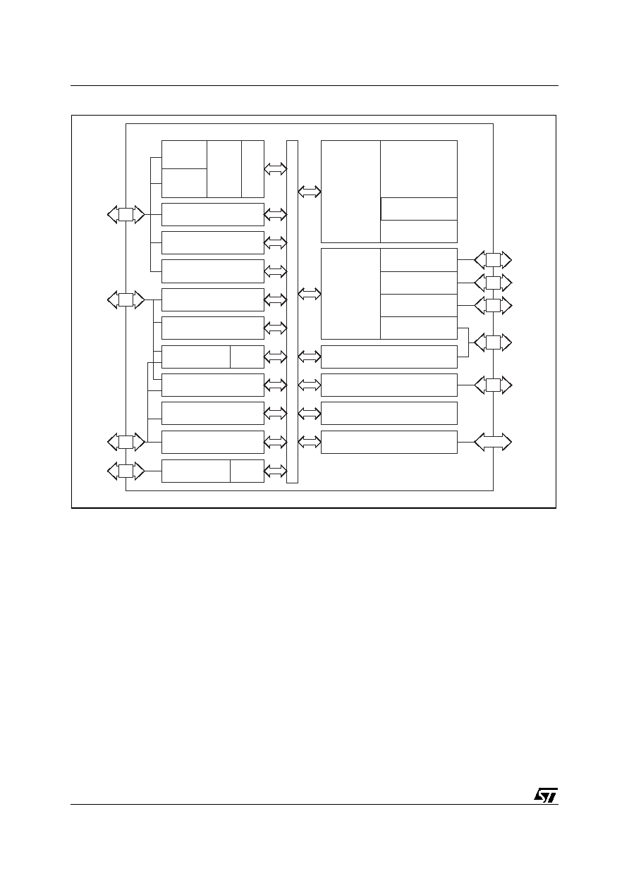
Figure 2. Block Diagram
PA0:7
PB0:7
PD1:2
PC0:7
MCU
Bus
P4.0:7
P1.0:7
P3.0:7
uPSD34xx
SYSTEM B
U
S
Dedicated
Pins
Supervisor:
Watchdog and Low-Voltage Reset
1st Flash Memory:
64K, 128K, or
256K Bytes
2nd Flash Memory:
32K Bytes
SRAM:
4K or 8K Bytes
Programmable
Decode and
Page Logic
General
Purpose
Programmable
Logic,
16 Macrocells
(8) GPIO, Port A
(80-pin only)
(8) GPIO, Port B
(4) GPIO, Port C
(2) GPIO, Port D
JTAG ICE and ISP
8032 Address/Data/Control Bus
(80-pin device only)
V
CC
, V
DD
, GND, Reset, Crystal In
Turbo
8032
Core
PFQ
&
BC
(3) 16-bit
Timer/
Counters
(2)
External
Interrupts
I
2
C
SPI
(8) 10-bit ADC
UART0
(8) GPIO, Port 1
(8) GPIO, Port 3
(8) GPIO, Port 4
USB+,
USB≠
USB v2.0,
Full Speed
10
FIFOs
UART1
Optional IrDA
Encoder/Decoder
16-bit PCA
(6) PWM, CAPCOM, TIMER
AI09695
9/264
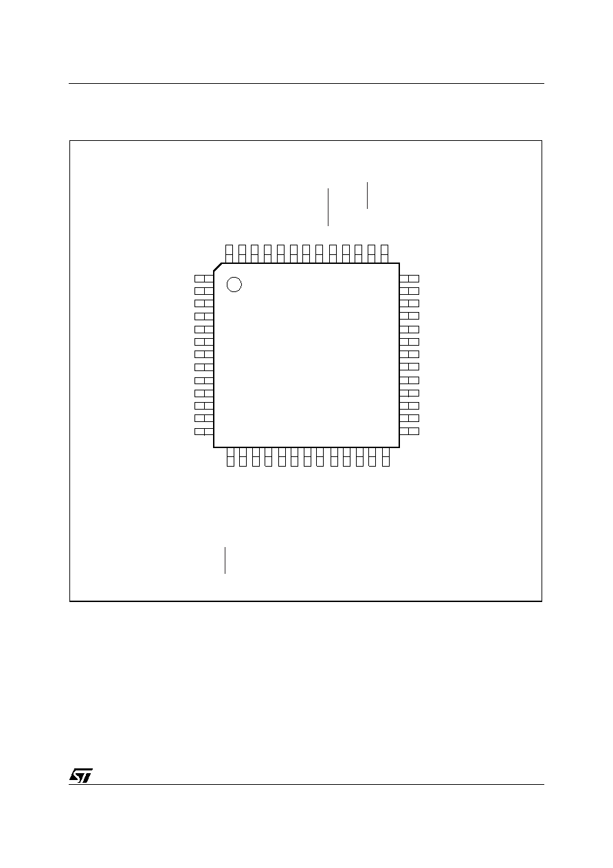
uPSD34xx - PIN DESCRIPTIONS
PIN DESCRIPTIONS
Figure 3. TQFP52 Connections
Note: 1. For 5V applications, V
DD
must be connected to a 5.0V source. For 3.3V applications, V
DD
must be connected to a 3.3V source.
2. These signals can be used on one of two different ports (Port 1 or Port 4) for flexibility. Default is Port1.
3. AV
REF
and 3.3V AV
CC
are shared in the 52-pin package only. ADC channels must use 3.3V as AV
REF
for the 52-pin package.
39 P1.5/SPIRXD
(2)
/ADC5
38 P1.4/SPICLK
(2)
/ADC4
37 P1.3/TXD1(IrDA)
(2)
/ADC3
36 P1.2/RXD1(IrDA)
(2)
/ADC2
35 P1.1/T2X
(2)
/ADC1
34 P1.0/T2
(2)
/ADC0
33 V
DD
(1)
32 XTAL2
31 XTAL1
30 P3.7/SCL
29 P3.6/SDA
28 P3.5/C1
27 P3.4/C0
PD1/CLKIN
PC7
JTAG TDO
JTAG TDI
DEBUG
3.3V V
CC
USB+
V
DD
(1)
GND
USB≠
PC2/V
STBY
JTAG TCK
JTAG TMS
1
2
3
4
5
6
7
8
9
10
11
12
13
52
51
50
49
48
47
46
45
44
43
42
41
40
PB0
PB1
PB2
PB3
PB4
AV
CC
/V
REF
(3)
PB5
GND
RESET_IN
PB6
PB7
P1.7/SPISEL
(2)
/ADC7
P1.6/SPITXD
(2)
/ADC6
14
15
16
17
18
19
20
21
22
23
24
25
26
SPISEL
(2)
/PCACLK1/P4.7
SPITXD
(2)
/TCM5/P4.6
SPIRXD
(2)
/TCM4/P4.5
SPICLK
(2)
/TCM3/P4.4
TXD1(IrDA)
(2)
/PCACLK0/P4.3
GND
RXD1(IrDA)
(2)
/TCM2/P4.2
T2X
(2)
/TCM1/P4.1
T2
(2)
/TCM0/P4.0
RXD0/P3.0
TXD0/P3.1
EXTINT0/TG0/P3.2
EXTINT1/TG1/P3.3
AI09696
uPSD34xx - PIN DESCRIPTIONS
10/264
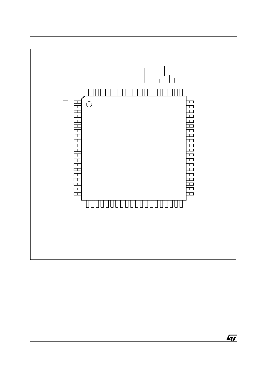
Figure 4. TQFP80 Connections
Note: NC = Not Connected
Note: 1. The USB+ pin needs a 1.5k
pull-up resistor.
2. For 5V applications, V
DD
must be connected to a 5.0V source. For 3.3V applications, V
DD
must be connected to a 3.3V source.
3. These signals can be used on one of two different ports (Port 1 or Port 4) for flexibility. Default is Port1.
60 P1.5/SPIRXD
(3)
/ADC5
59 P1.4/SPICLK
(3)
/ADC4
58 P1.3/TXD1(IrDA)
(3)
/ADC3
57 NC
56 P1.2/RXD1(IrDA)
(3)
/ADC2
55 NC
54 P1.1/T2X
(3)
/ADC1
53 NC
52 P1.0/T2
(3)
/ADC0
51 NC
50 V
DD
(1)
49 XTAL2
48 XTAL1
47 MCU AD7
46 P3.7/SCL
45 MCU AD6
44 P3.6/SDA
43 MCU AD5
42 P3.5/C1
41 MCU AD4
PD2/CSI
P3.3/TG1/EXINT1
PD1/CLKIN
ALE
PC7
JTAG TDO
JTAG TDI
DEBUG
PC4/TERR
3.3V V
CC
USB+
(1)
V
DD
(2)
GND
USB≠
PC3/TSTAT
PC2/V
STBY
JTAG TCK
SPISEL
(2)
/PCACLK1/P4.7
SPITXD
(2)
/TCM5/P4.6
JTAG TMS
1
2
3
4
5
6
7
8
9
10
11
12
13
14
15
16
17
18
19
20
80
79
78
77
76
75
74
73
72
71
70
69
68
67
66
65
64
63
62
61
PB0
P3.2/EXINT0/TG0
PB1
P3.1/TXD0
PB2
P3.0/RXD0
PB3
PB4
AV
CC
PB5
V
REF
GND
RESET_IN
PB6
PB7
RD
P1.7/SPISEL
(3)
/ADC7
PSEN
WR
P1.6/SPITXD
(3)
/ADC6
21
22
23
24
25
26
27
28
29
30
31
32
33
34
35
36
37
38
39
40
PA7
PA6
SPIRXD
(2)
/TCM4/P4.5
PA5
SPICLK
(2)
/TCM3/P4.4
PA4
TXD1(IrDA)
(2)
/PCACLK0/P4.3
PA3
GND
RXD1(IrDA)
(2)
/TCM2/P4.2
T2X
(2)
/TCM1/P4.1
PA2
T2
(2)
/TCM0/P4.0
PA1
PA0
MCU AD0
MCU AD1
MCU AD2
MCU AD3
P3.4/C0
AI09697

11/264
uPSD34xx - PIN DESCRIPTIONS
Table 2. Pin Definitions
Port Pin
Signal
Name
80-Pin
No.
52-Pin
No.
(1)
In/Out
Function
Basic
Alternate 1
Alternate 2
MCUAD0
AD0
36
N/A
I/O
External Bus
Multiplexed Address/
Data bus A0/D0
MCUAD1
AD1
37
N/A
I/O
Multiplexed Address/
Data bus A1/D1
MCUAD2
AD2
38
N/A
I/O
Multiplexed Address/
Data bus A2/D2
MCUAD3
AD3
39
N/A
I/O
Multiplexed Address/
Data bus A3/D3
MCUAD4
AD4
41
N/A
I/O
Multiplexed Address/
Data bus A4/D4
MCUAD5
AD5
43
N/A
I/O
Multiplexed Address/
Data bus A5/D5
MCUAD6
AD6
45
N/A
I/O
Multiplexed Address/
Data bus A6/D6
MCUAD7
AD7
47
N/A
I/O
Multiplexed Address/
Data bus A7/D7
P1.0
T2
ADC0
52
34
I/O
General I/O port pin
Timer 2 Count input
(T2)
ADC Channel 0
input (ADC0)
P1.1
T2X
ADC1
54
35
I/O
General I/O port pin
Timer 2 Trigger input
(T2X)
ADC Channel 1
input (ADC1)
P1.2
RxD1
ADC2
56
36
I/O
General I/O port pin
UART1 or IrDA
Receive (RxD1)
ADC Channel 2
input (ADC2)
P1.3
TXD1
ADC3
58
37
I/O
General I/O port pin
UART or IrDA
Transmit (TxD1)
ADC Channel 3
input (ADC3)
P1.4
SPICLK
ADC4
59
38
I/O
General I/O port pin
SPI Clock Out
(SPICLK)
ADC Channel 4
input (ADC4)
P1.5
SPIRxD
ADC6
60
39
I/O
General I/O port pin
SPI Receive
(SPIRxD)
ADC Channel 5
input (ADC5)
P1.6
SPITXD
ADC6
61
40
I/O
General I/O port pin
SPI Transmit
(SPITxD)
ADC Channel 6
input (ADC6)
P1.7
SPISEL
ADC7
64
41
I/O
General I/O port pin
SPI Slave Select
(SPISEL)
ADC Channel 7
input (ADC7)
P3.0
RxD0
75
23
I/O
General I/O port pin
UART0 Receive
(RxD0)
P3.1
TXD0
77
24
I/O
General I/O port pin
UART0 Transmit
(TxD0)
P3.2
EXINT0
TGO
79
25
I/O
General I/O port pin
Interrupt 0 input
(EXTINT0)/Timer 0
gate control (TG0)
P3.3
INT1
2
26
I/O
General I/O port pin
Interrupt 1 input
(EXTINT1)/Timer 1
gate control (TG1)
P3.4
C0
40
27
I/O
General I/O port pin
Counter 0 input (C0)
P3.5
C1
42
28
I/O
General I/O port pin
Counter 1 input (C1)
P3.6
SDA
44
29
I/O
General I/O port pin
I
2
C Bus serial data
(I
2
CSDA)
P3.7
SCL
46
30
I/O
General I/O port pin
I
2
C Bus clock
(I
2
CSCL)
P4.0
T2
TCM0
33
22
I/O
General I/O port pin
Program Counter
Array0 PCA0-TCM0
Timer 2 Count input
(T2)

uPSD34xx - PIN DESCRIPTIONS
12/264
P4.1
T2X
TCM1
31
21
I/O
General I/O port pin
PCA0-TCM1
Timer 2 Trigger input
(T2X)
P4.2
RXD1
TCM2
30
20
I/O
General I/O port pin
PCA0-TCM2
UART1 or IrDA
Receive (RxD1)
P4.3
TXD1
PCACLK0
27
18
I/O
General I/O port pin
PCACLK0
UART1 or IrDA
Transmit (TxD1)
P4.4
SPICLK
TCM3
25
17
I/O
General I/O port pin
Program Counter
Array1 PCA1-TCM3
SPI Clock Out
(SPICLK)
P4.5
SPIRXD
TCM4
23
16
I/O
General I/O port pin
PCA1-TCM4
SPI Receive
(SPIRxD)
P4.6
SPITXD
19
15
I/O
General I/O port pin
PCA1-TCM5
SPI Transmit
(SPITxD)
P4.7
SPISEL
PCACLK1
18
14
I/O
General I/O port pin
PCACLK1
SPI Slave Select
(SPISEL)
V
REF
70
N/A
I
Reference Voltage
input for ADC
RD
65
N/A
O
READ Signal,
external bus
WR
62
N/A
O
WRITE Signal,
external bus
PSEN
63
N/A
O
PSEN Signal,
external bus
ALE
4
N/A
O
Address Latch
signal, external bus
RESET_IN
68
44
I
Active low reset
input
XTAL1
48
31
I
Oscillator input pin
for system clock
XTAL2
49
32
O
Oscillator output pin
for system clock
DEBUG
8
5
I/O
I/O to the MCU
Debug Unit
PA0
35
N/A
I/O
General I/O port pin
All Port A pins
support:
1.
PLD Macro-cell
outputs, or
2.
PLD inputs, or
3.
Latched
Address Out
(A0-A7), or
4.
Peripheral I/O
Mode
PA1
34
N/A
I/O
General I/O port pin
PA2
32
N/A
I/O
General I/O port pin
PA3
28
N/A
I/O
General I/O port pin
PA4
26
N/A
I/O
General I/O port pin
PA5
24
N/A
I/O
General I/O port pin
PA6
22
N/A
I/O
General I/O port pin
PA7
21
N/A
I/O
General I/O port pin
PB0
80
52
I/O
General I/O port pin
All Port B pins
support:
1.
PLD Macro-cell
outputs, or
2.
PLD inputs, or
3.
Latched
Address Out
(A0-A7)
PB1
78
51
I/O
General I/O port pin
PB2
76
50
I/O
General I/O port pin
PB3
74
49
I/O
General I/O port pin
PB4
73
48
I/O
General I/O port pin
PB5
71
46
I/O
General I/O port pin
PB6
67
43
I/O
General I/O port pin
PB7
66
42
I/O
General I/O port pin
JTAGTMS
TMS
20
13
I
JTAG pin (TMS)
JTAGTCK
TCK
17
12
I
JTAG pin (TCK)
Port Pin
Signal
Name
80-Pin
No.
52-Pin
No.
(1)
In/Out
Function
Basic
Alternate 1
Alternate 2

13/264
uPSD34xx - PIN DESCRIPTIONS
Note: 1. N/A = Signal Not Available on 52-pin package.
PC2
V
STBY
16
11
I/O
General I/O port pin
SRAM Standby
voltage input
(V
STBY
)
PLD Macrocell
output, or PLD input
PC3
TSTAT
15
N/A
I/O
General I/O port pin
Optional JTAG
Status (TSTAT)
PLD, Macrocell
output, or PLD input
PC4
TERR
9
N/A
I/O
General I/O port pin
Optional JTAG
Status (TERR)
PLD, Macrocell
output, or PLD input
JTAGTDI
TDI
7
4
I
JTAG pin (TDI)
JTAGTDO
TDO
6
3
O
JTAG pin (TDO)
PC7
5
2
I/O
General I/O port pin
PLD, Macrocell
output, or PLD input
PD1
CLKIN
3
1
I/O
General I/O port pin
1.
PLD I/O
2.
Clock input to
PLD and APD
PD2
CSI
1
N/A
I/O
General I/O port pin
1.
PLD I/O
2.
Chip select ot
PSD Module
USB+
11
7
I/O
USB D+ pin; 1.5k
pull-up resistor is
required.
USB≠
14
10
I/O
USB D≠ pin
3.3V-V
CC
10
6
V
CC
- MCU Module
AV
CC
72
47
Analog V
CC
Input
V
DD
3.3V or 5V
12
8
V
DD
- PSD Module
V
DD
- 3.3V for 3V
V
DD
- 5V for 5V
V
DD
3.3V or 5V
50
33
V
DD
- PSD Module
V
DD
- 3.3V for 3V
V
DD
- 5V for 5V
GND
13
9
GND
29
19
GND
69
45
NC
11
N/A
NC
51
N/A
NC
53
N/A
NC
55
N/A
NC
57
N/A
Port Pin
Signal
Name
80-Pin
No.
52-Pin
No.
(1)
In/Out
Function
Basic
Alternate 1
Alternate 2
uPSD34xx - HARDWARE DESCRIPTION
14/264
HARDWARE DESCRIPTION
The uPSD34xx has a modular architecture built
from a stacked die process. There are two die, one
is designated "MCU Module" in this document, and
the other is designated "PSD Module" (see
Figure
5., page 15
). In all cases, the MCU Module die op-
erates at 3.3V with 5V tolerant I/O. The PSD Mod-
ule is either a 3.3V die or a 5V die, depending on
the uPSD34xx device as described below.
The MCU Module consists of a fast 8032 core, that
operates with 4 clocks per instruction cycle, and
has many peripheral and system supervisor func-
tions. The PSD Module provides the 8032 with
multiple memories (two Flash and one SRAM) for
program and data, programmable logic for ad-
dress decoding and for general-purpose logic, and
additional I/O. The MCU Module communicates
with the PSD Module through internal address and
data busses (AD0 ≠ AD15) and control signals
(RD, WR, PSEN, ALE, RESET).
There are slightly different I/O characteristics for
each module. I/Os for the MCU module are desig-
nated as Ports 1, 3, and 4. I/Os for the PSD Mod-
ule are designated as Ports A, B, C, and D.
For all 5V uPSD34xx devices, a 3.3V MCU Module
is stacked with a 5V PSD Module. In this case, a
5V uPSD34xx device must be supplied with
3.3V
CC
for the MCU Module and 5.0V
DD
for the
PSD Module. Ports 3 and 4 of the MCU Module
are 3.3V ports with tolerance to 5V devices (they
can be directly driven by external 5V devices and
they can directly drive external 5V devices while
producing a V
OH
of 2.4V min and V
CC
max). Ports
A, B, C, and D of the PSD Module are true 5V
ports.
For all 3.3V uPSD34xxV devices, a 3.3V MCU
Module is stacked with a 3.3V PSD Module. In this
case, a 3.3V uPSD34xx device needs to be sup-
plied with a single 3.3V voltage source at both V
CC
and V
DD
. I/O pins on Ports 3 and 4 are 5V tolerant
and can be connected to external 5V peripherals
devices if desired. Ports A, B, C, and D of the PSD
Module are 3.3V ports, which are not tolerant to
external 5V devices.
Refer to Table 3 for port type and voltage source
requirements.
80-pin uPSD34xx devices provide access to 8032
address, data, and control signals on external pins
to connect external peripheral and memory devic-
es. 52-pin uPSD34xx devices do not provide ac-
cess to the 8032 system bus.
All non-volatile memory and configuration portions
of the uPSD34xx device are programmed through
the JTAG interface and no special programming
voltage is needed. This same JTAG port is also
used for debugging of the 8032 core at runtime
providing breakpoint, single-step, display, and
trace features. A non-volatile security bit may be
programmed to block all access via JTAG inter-
face for security. The security bit is defeated only
by erasing the entire device, leaving the device
blank and ready to use again.
Table 3. Port Type and Voltage Source Combinations
Device Type
V
CC
for MCU
Module
V
DD
for PSD
Module
Ports 1, 3, and 4 on MCU
Module
Ports A, B, C, and D on
PSD Module
5V:
uPSD34xx
3.3V
5.0V
3.3V (Ports 3 and 4 are
5V tolerant)
5V
3.3V:
uPSD34xxV
3.3V
3.3V
3.3V (Ports 3 and 4 are
5V tolerant)
3.3V. NOT 5V tolerant

15/264
uPSD34xx - HARDWARE DESCRIPTION
Figure 5. Functional Modules
10-bit
ADC
Dedicated Memory
Interface Prefetch,
Branch Cache
Enhanced MCU Interface
Decode PLD
PSD Page Register
SRAM
CPLD - 16 MACROCELLS
JTAG ISP
Reset Logic
WDT
Internal
Reset
Port 1
Port 3
Dual
UARTs
Interrupt
3 Timer /
Counters
256 Byte SRAM
Turbo 8032 Core
PSD Internal Bus
8032 Internal Bus
PSD
Reset
LVD
I
2
C
Unit
USB and
Trans-
ceiver
Port D
GPIO
Port C
JTAG and
GPIO
Secondary
Flash
Reset Input
uPSD34xx
JTAG
DEBUG
8-Bit/16-Bit
Die-to-Die Bus
Main Flash
PCA
PWM
Counters
Reset
Pin
Ext.
Bus
SPI
V
CC
Pins
3.3V
V
DD
Pins
3.3V or 5V
MCU Module
PSD Module
Port 3 - UART0,
Intr, Timers
Port 1 - Timer, ADC, SPI
Port 4 - PCA,
PWM, UART1
Port 3
I
2
C
USB
pins
XTAL
Clock Unit
Port A,B,C PLD
I/O and GPIO
AI10409
uPSD34xx - MEMORY ORGANIZATION
16/264
MEMORY ORGANIZATION
The 8032 MCU core views memory on the MCU
module as "internal" memory and it views memory
on the PSD module as "external" memory, see
Figure 6.
Internal memory on the MCU Module consists of
DATA, IDATA, and SFRs. These standard 8032
memories reside in 384 bytes of SRAM located at
a fixed address space starting at address 0x0000.
External memory on the PSD Module consists of
four types: main Flash (64K, 128K, or 256K bytes),
a smaller secondary Flash (32K), SRAM (4K or 8K
bytes), and a block of PSD Module control regis-
ters called csiop (256 bytes). These external mem-
ories reside at programmable address ranges,
specified using the software tool PSDsoft Express.
See the PSD Module section of this document for
more details on these memories.
External memory is accessed by the 8032 in two
separate 64K byte address spaces. One address
space is for program memory and the other ad-
dress space is for data memory. Program memory
is accessed using the 8032 signal, PSEN. Data
memory is accessed using the 8032 signals, RD
and WR. If the 8032 needs to access more than
64K bytes of external program or data memory, it
must use paging (or banking) techniques provided
by the Page Register in the PSD Module.
Note: When referencing program and data mem-
ory spaces, it has nothing to do with 8032 internal
SRAM areas of DATA, IDATA, and SFR on the
MCU Module. Program and data memory spaces
only relate to the external memories on the PSD
Module.
External memory on the PSD Module can overlap
the internal SRAM memory on the MCU Module in
the same physical address range (starting at
0x0000) without interference because the 8032
core does not assert the RD or WR signals when
accessing internal SRAM.
Figure 6. uPSD34xx Memories
∑ External memories may be placed at virtually
any address using software tool PSDsoft Express.
∑ The SRAM and Flash memories may be placed
in 8032 Program Space or Data Space using
PSDsoft Express.
∑ Any memory in 8032 Data Space is XDATA.
64KB
or
128KB
or
256KB
32KB
Main
Flash
Internal SRAM on
MCU Module
External Memory on
PSD Module
IDATA
SFR
DATA
Secondary
Flash
4KB
or
8KB
SRAM
384 Bytes SRAM
Direct or Indirect Addressing
FF
80
7F
128 Bytes
128 Bytes
128 Bytes
0
Indirect
Addressing
Fixed
Addresses
Direct
Addressing
AI10410

17/264
uPSD34xx - MEMORY ORGANIZATION
Internal Memory (MCU Module, Standard 8032
Memory: DATA, IDATA, SFR)
DATA Memory. The first 128 bytes of internal
SRAM ranging from address 0x0000 to 0x007F
are called DATA, which can be accessed using
8032 direct or indirect addressing schemes and
are typically used to store variables and stack.
Four register banks, each with 8 registers (R0 ≠
R7), occupy addresses 0x0000 to 0x001F. Only
one of these four banks may be enabled at a time.
The next 16 locations at 0x0020 to 0x002F contain
128 directly addressable bit locations that can be
used as software flags. SRAM locations 0x0030
and above may be used for variables and stack.
IDATA Memory. The next 128 bytes of internal
SRAM are named IDATA and range from address
0x0080 to 0x00FF. IDATA can be accessed only
through 8032 indirect addressing and is typically
used to hold the MCU stack as well as data vari-
ables. The stack can reside in both DATA and
IDATA memories and reach a size limited only by
the available space in the combined 256 bytes of
these two memories (since stack accesses are al-
ways done using indirect addressing, the bound-
ary between DATA and IDATA does not exist with
regard to the stack).
SFR Memory. Special Function Registers (
Table
5., page 25
) occupy a separate physical memory,
but they logically overlap the same 128 bytes as
IDATA, ranging from address 0x0080 to 0x00FF.
SFRs are accessed only using direct addressing.
There 86 active registers used for many functions:
changing the operating mode of the 8032 MCU
core, controlling 8032 peripherals, controlling I/O,
and managing interrupt functions. The remaining
unused SFRs are reserved and should not be ac-
cessed.
16 of the SFRs are both byte- and bit-addressable.
Bit-addressable SFRs are those whose address
ends in "0" or "8" hex.
External Memory (PSD Module: Program
memory, Data memory)
The PSD Module has four memories: main Flash,
secondary Flash, SRAM, and csiop. See the PSD
MODULE section for more detailed information on
these memories.
Memory mapping in the PSD Module is imple-
mented with the Decode PLD (DPLD) and option-
ally the Page Register. The user specifies decode
equations for individual segments of each of the
memories using the software tool PSDsoft Ex-
press. This is a very easy point-and-click process
allowing total flexibility in mapping memories. Ad-
ditionally, each of the memories may be placed in
various combinations of 8032 program address
space or 8032 data address space by using the
software tool PSDsoft Express.
Program Memory. External program memory is
addressed by the 8032 using its 16-bit Program
Counter (PC) and is accessed with the 8032 sig-
nal, PSEN. Program memory can be present at
any address in program space between 0x0000
and 0xFFFF.
After a power-up or reset, the 8032 begins pro-
gram execution from location 0x0000 where the
reset vector is stored, causing a jump to an initial-
ization routine in firmware. At address 0x0003, just
following the reset vector are the interrupt service
locations. Each interrupt is assigned a fixed inter-
rupt service location in program memory. An inter-
rupt causes the 8032 to jump to that service
location, where it commences execution of the
service routine. External Interrupt 0 (EXINT0), for
example, is assigned to service location 0x0003. If
EXINT0 is going to be used, its service routine
must begin at location 0x0003. Interrupt service lo-
cations are spaced at 8-byte intervals: 0x0003 for
EXINT0, 0x000B for Timer 0, 0x0013 for EXINT1,
and so forth. If an interrupt service routine is short
enough, it can reside entirely within the 8-byte in-
terval. Longer service routines can use a jump in-
struction to somewhere else in program memory.
Data Memory. External data is referred to as
XDATA and is addressed by the 8032 using Indi-
rect Addressing via its 16-bit Data Pointer Register
(DPTR) and is accessed by the 8032 signals, RD
and WR. XDATA can be present at any address in
data space between 0x0000 and 0xFFFF.
Note: the uPSD34xx has dual data pointers
(source and destination) making XDATA transfers
much more efficient.
Memory Placement. PSD Module architecture
allows the placement of its external memories into
different combinations of program memory and
data memory spaces. This means the main Flash,
the secondary Flash, and the SRAM can be
viewed by the 8032 MCU in various combinations
of program memory or data memory as defined by
PSDsoft Express.
As an example of this flexibility, for applications
that require a great deal of Flash memory in data
space (large lookup tables or extended data re-
cording), the larger main Flash memory can be
placed in data space and the smaller secondary
Flash memory can be placed in program space.
The opposite can be realized for a different appli-
cation if more Flash memory is needed for code
and less Flash memory for data.

uPSD34xx - 8032 MCU CORE PERFORMANCE ENHANCEMENTS
18/264
By default, the SRAM and csiop memories on the
PSD Module must always reside in data memory
space and they are treated by the 8032 as XDA-
TA.
The main Flash and secondary Flash memories
may reside in program space, data space, or both.
These memory placement choices specified by
PSDsoft Express are programmed into non-vola-
tile sections of the uPSD34xx, and are active at
power-up and after reset. It is possible to override
these initial settings during runtime for In-Applica-
tion Programming (IAP).
Standard 8032 MCU architecture cannot write to
its own program memory space to prevent acci-
dental corruption of firmware. However, this be-
comes an obstacle in typical 8032 systems when
a remote update to firmware in Flash memory is
required using IAP. The PSD module provides a
solution for remote updates by allowing 8032 firm-
ware to temporarily "reclassify" Flash memory to
reside in data space during a remote update, then
returning Flash memory back to program space
when finished. See the VM Register (
Table
104., page 174
) in the PSD Module section of this
document for more details.
8032 MCU CORE PERFORMANCE ENHANCEMENTS
Before describing performance features of the
uPSD34xx, let us first look at standard 8032 archi-
tecture. The clock source for the 8032 MCU cre-
ates a basic unit of timing called a machine-cycle,
which is a period of 12 clocks for standard 8032
MCUs. The instruction set for traditional 8032
MCUs consists of 1, 2, and 3 byte instructions that
execute in different combinations of 1, 2, or 4 ma-
chine-cycles. For example, there are one-byte in-
structions that execute in one machine-cycle (12
clocks), one-byte instructions that execute in four
machine-cycles (48 clocks), two-byte, two-cycle
instructions (24 clocks), and so on. In addition,
standard 8032 architecture will fetch two bytes
from program memory on almost every machine-
cycle, regardless if it needs them or not (dummy
fetch). This means for one-byte, one-cycle instruc-
tions, the second byte is ignored. These one-byte,
one-cycle instructions account for half of the
8032's instructions (126 out of 255 opcodes).
There are inefficiencies due to wasted bus cycles
and idle bus times that can be eliminated.
The uPSD34xx 8032 MCU core offers increased
performance in a number of ways, while keeping
the exact same instruction set as the standard
8032 (all opcodes, the number of bytes per in-
struction, and the native number a machine-cycles
per instruction are identical to the original 8032).
The first way performance is boosted is by reduc-
ing the machine-cycle period to just 4 MCU clocks
as compared to 12 MCU clocks in a standard
8032. This shortened machine-cycle improves the
instruction rate for one- or two-byte, one-cycle in-
structions by a factor of three (
Figure 7., page 19
)
compared to standard 8051 architectures, and sig-
nificantly improves performance of multiple-cycle
instruction types.
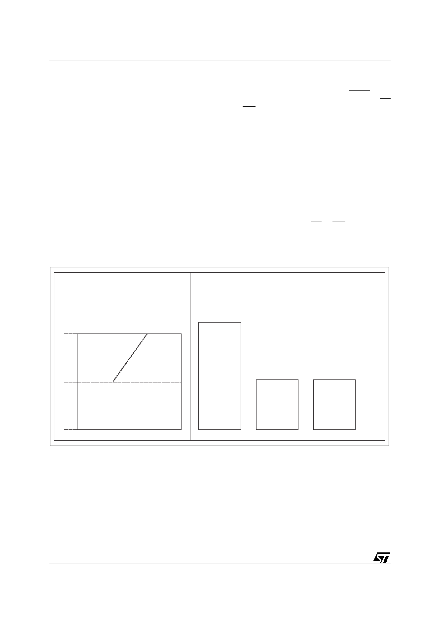
The example in Figure
7
shows a continuous exe-
cution stream of one- or two-byte, one-cycle in-
structions. The 5V uPSD34xx will yield 10 MIPS
peak performance in this case while operating at
40MHz clock rate. In a typical application however,
the effective performance will be lower since pro-
grams do not use only one-cycle instructions, but
special techniques are implemented in the
uPSD34xx to keep the effective MIPS rate as
close as possible to the peak MIPS rate at all
times. This is accomplished with an instruction
Pre-Fetch Queue (PFQ), a Branch Cache (BC),
and a 16-bit program memory bus as shown in
Figure 8., page 19
.

19/264
uPSD34xx - 8032 MCU CORE PERFORMANCE ENHANCEMENTS
Figure 7. Comparison of uPSD34xx with Standard 8032 Performance
Figure 8. Instruction Pre-Fetch Queue and Branch Cache
MCU Clock
Standard 8032
Fetch Byte for Instruction A
Execute Instruction A
and Fetch a Second Dummy Byte
Turbo uPSD34xx
Execute Instruction and
Pre-Fetch Next Instruction
4 clocks (one machine cycle)
12 clocks (one machine cycle)
1- or 2-byte, 1-cycle Instructions
Dummy Byte is Ignored (wasted bus access)
Execute Instruction and
Pre-Fetch Next Instruction
Execute Instruction and
Pre-Fetch Next Instruction
Instruction A
Instruction B
Instruction C
Instruction A
Turbo uPSD34xx executes instructions A, B, and C in the same
amount of time that a standard 8032 executes only Instruction A.
one machine cycle
one machine cycle
AI10411
Branch 4
Code
Branch 4
Code
8032
MCU
16-bit
Program
Memory
on PSD
Module
Instruction Pre-Fetch Queue (PFQ)
4 Bytes of Instruction
Instruction Byte
Wait
Wait
8
Instruction Byte
8
Instruction Byte
8
Current
Branch
Address
Compare
Branch
Cache
(BC)
16
AI10431
Address
16
16
16
Address
Load on Branch Address Match
Branch 3
Code
Branch 3
Code
Branch 2
Code
Branch 2
Code
Branch 1
Code
Branch 1
Code

uPSD34xx - 8032 MCU CORE PERFORMANCE ENHANCEMENTS
20/264
Pre-Fetch Queue (PFQ) and Branch Cache
(BC)
The PFQ is always working to minimize the idle
bus time inherent to 8032 MCU architecture, to
eliminate wasted memory fetches, and to maxi-
mize memory bandwidth to the MCU. The PFQ
does this by running asynchronously in relation to
the MCU, looking ahead to pre-fetch two bytes
(word) of code from program memory during any
idle bus periods. Only necessary word will be
fetched (no dummy fetches like standard 8032).
The PFQ will queue up to four code bytes in ad-
vance of execution, which significantly optimizes
sequential program performance. However, when
program execution becomes non-sequential (pro-
gram branch), a typical pre-fetch queue will empty
itself and reload new code, causing the MCU to
stall. The Turbo uPSD34xx diminishes this prob-
lem by using a Branch Cache with the PFQ. The
BC is a four-way, fully associative cache, meaning
that when a program branch occurs, its branch
destination address is compared simultaneously
with four recent previous branch destinations
stored in the BC. Each of the four cache entries
contain up to four bytes of code related to a
branch. If there is a hit (a match), then all four code
bytes of the matching program branch are trans-
ferred immediately and simultaneously from the
BC to the PFQ, and execution on that branch con-
tinues with minimal delay. This greatly reduces the
chance that the MCU will stall from an empty PFQ,
and improves performance in embedded control
systems where it is quite common to branch and
loop in relatively small code localities.
By default, the PFQ and BC are enabled after
power-up or reset. The 8032 can disable the PFQ
and BC at runtime if desired by writing to a specific
SFR (BUSCON).
The memory in the PSD module operates with
variable wait states depending on the value spec-
ified in the SFR named BUSCON. For example, a
5V uPSD34xx device operating at a 40MHz crystal
frequency requires four memory wait states (equal
to four MCU clocks). In this example, once the
PFQ has one word of code, the wait states be-
come transparent and a full 10 MIPS is achieved
when the program stream consists of sequential
one- or two-byte, one machine-cycle instructions
as shown in
Figure 7., page 19
(transparent be-
cause a machine-cycle is four MCU clocks which
equals the memory pre-fetch wait time that is also
four MCU clocks). But it is also important to under-
stand PFQ operation on multi-cycle instructions.
PFQ Example, Multi-cycle Instructions
Let us look at a string of two-byte, two-cycle in-
structions in
Figure 9., page 21
. There are three
instructions executed sequentially in this example,
instructions A, B, and C. Each of the time divisions
in the figure is one machine-cycle of four clocks,
and there are six phases to reference in this dis-
cussion. Each instruction is pre-fetched into the
PFQ in advance of execution by the MCU. Prior to
Phase 1, the PFQ has pre-fetched the two instruc-
tion bytes (A1 and A2) of Instruction A. During
Phase one, both bytes are loaded into the MCU
execution unit. Also in Phase 1, the PFQ is pre-
fetching Instruction B (bytes B1 and B2) from pro-
gram memory. In Phase 2, the MCU is processing
Instruction A internally while the PFQ is pre-fetch-
ing Instruction C. In Phase 3, both bytes of instruc-
tion B are loaded into the MCU execution unit and
the PFQ begins to pre-fetch bytes for the next in-
struction. In Phase 4 Instruction B is processed.
The uPSD34xx MCU instructions are an exact 1/3
scale of all standard 8032 instructions with regard
to number of cycles per instruction.
Figure
10., page 21
shows the equivalent instruction se-
quence from the example above on a standard
8032 for comparison.
Aggregate Performance
The stream of two-byte, two-cycle instructions in
Figure 9., page 21
, running on a 40MHz, 5V,
uPSD34xx will yield 5 MIPs. And we saw the
stream of one- or two-byte, one-cycle instructions
in
Figure 7., page 19
, on the same MCU yield 10
MIPs. Effective performance will depend on a
number of things: the MCU clock frequency; the
mixture of instructions types (bytes and cycles) in
the application; the amount of time an empty PFQ
stalls the MCU (mix of instruction types and miss-
es on Branch Cache); and the operating voltage.
A 5V uPSD34xx device operates with four memory
wait states, but a 3.3V device operates with five
memory wait states yielding 8 MIPS peak com-
pared to 10 MIPs peak for 5V device. The same
number of wait states will apply to both program
fetches and to data READ/WRITEs unless other-
wise specified in the SFR named BUSCON.
In general, a 3X aggregate performance increase
is expected over any standard 8032 application
running at the same clock frequency.

21/264
uPSD34xx - 8032 MCU CORE PERFORMANCE ENHANCEMENTS
Figure 9. PFQ Operation on Multi-cycle Instructions
Figure 10. uPSD34xx Multi-cycle Instructions Compared to Standard 8032
Three 2-byte, 2-cycle Instructions on uPSD34xx
PFQ
MCU
Execution
Inst A, Byte 1&2 Inst B, Byte 1&2 Inst C, Byte 1&2
Next Inst
Previous Instruction
A1
A2
Process A
B1
B2
Process B
C1
C2
AI10432
Process C
Continue to Pre-Fetch
Next Inst
4-clock
Macine Cycle
Instruction A
Instruction B
Instruction C
Pre-Fetch
Inst A
Pre-Fetch Inst B and C
Pre-Fetch next Inst
Phase 1
Phase 2
Phase 3
Phase 4
Phase 6
Phase 5
A1
A2
Inst A
B1
B2
Inst B
C1 C2
Inst C
Three 2-byte, 2-cycle Instructions, uPSD34xx vs. Standard 8032
uPSD34xx
Std 8032
72 Clocks (12 clocks per cycle)
24 Clocks Total (4 clocks per cycle)
Byte 1
Byte 2
Process Inst A
Byte 1
Byte 2
Process Inst B
Byte 1
Byte 2
Process Inst C
AI10412
1 Cycle
1 Cycle
uPSD34xx - MCU MODULE DISCRIPTION
22/264
MCU MODULE DISCRIPTION
This section provides a detail description of the
MCU Module system functions and peripherals, in-
cluding:
8032 MCU Registers
Special Function Registers
8032 Addressing Modes
uPSD34xx Instruction Set Summary
Dual Data Pointers
Debug Unit
Interrupt System
MCU Clock Generation
Power Saving Modes
Oscillator and External Components
I/O Ports
MCU Bus Interface
Supervisory Functions
Standard 8032 Timer/Counters
Serial UART Interfaces
IrDA Interface
I
2
C Interface
SPI Interface
Analog to Digital Converter
Programmable Counter Array (PCA)
USB Interface
Note: A full description of the 8032 instruction set
may be found in the uPSD34xx Programmers
Guide.
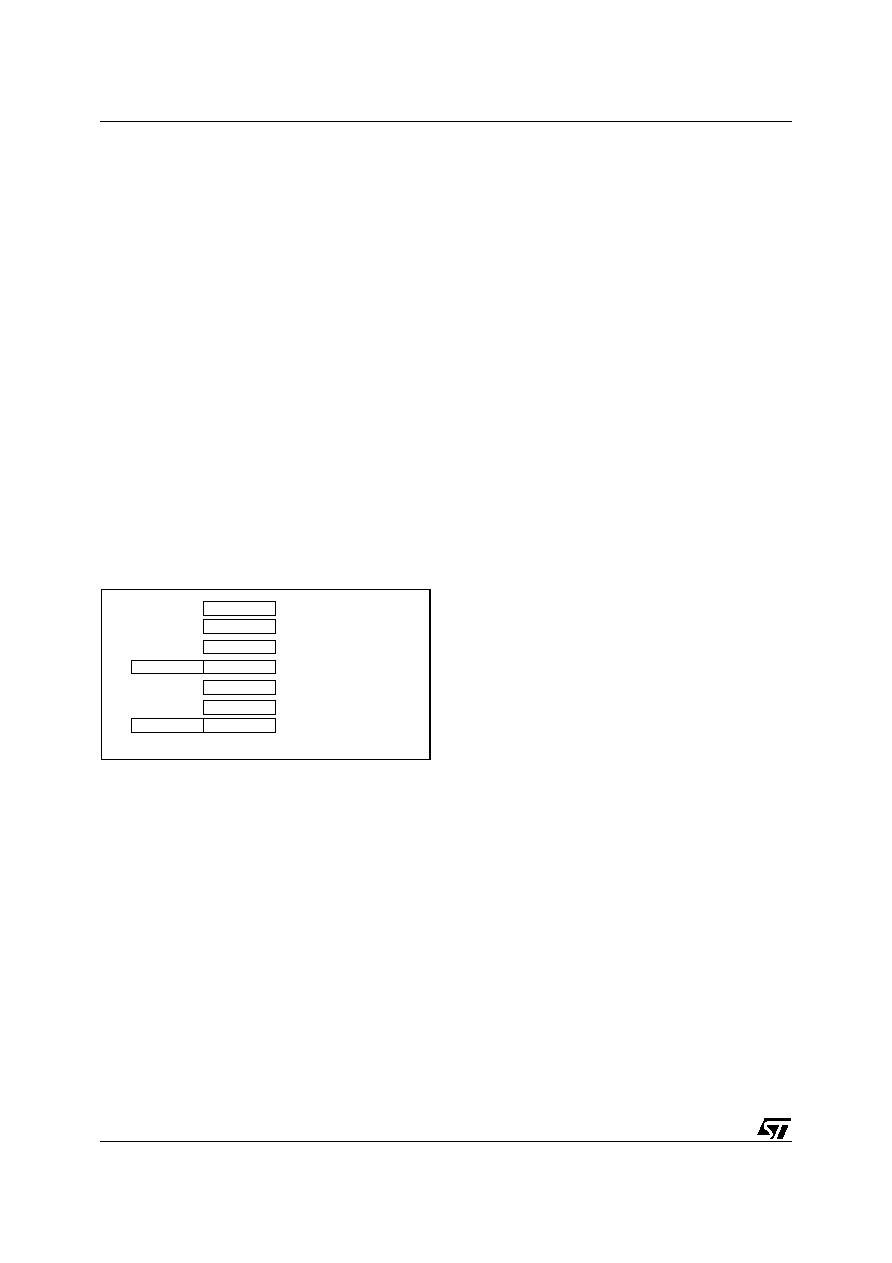
8032 MCU REGISTERS
The uPSD34xx has the following 8032 MCU core
registers, also shown in Figure
11
.
Figure 11. 8032 MCU Registers
Stack Pointer (SP)
The SP is an 8-bit register which holds the current
location of the top of the stack. It is incremented
before a value is pushed onto the stack, and dec-
remented after a value is popped off the stack. The
SP is initialized to 07h after reset. This causes the
stack to begin at location 08h (top of stack). To
avoid overlapping conflicts, the user must initialize
the top of the stack to 20h if all four banks of reg-
isters R0 - R7 are used, as well as the top of stack
to 30h if all of the 8032 bit memory locations are
used.
Data Pointer (DPTR)
DPTR is a 16-bit register consisting of two 8-bit
registers, DPL and DPH. The DPTR Register is
used as a base register to create an address for in-
direct jumps, table look-up operations, and for ex-
ternal data transfers (XDATA). When not used for
addressing, the DPTR Register can be used as a
general purpose 16-bit data register.
Very frequently, the DPTR Register is used to ac-
cess XDATA using the External Direct addressing
mode. The uPSD34xx has a special set of SFR
registers (DPTC, DPTM) to control a secondary
DPTR Register to speed memory-to-memory
XDATA transfers. Having dual DPTR Registers al-
lows rapid switching between source and destina-
tion addresses (see details in
DUAL DATA
POINTERS, page 38
).
Program Counter (PC)
The PC is a 16-bit register consisting of two 8-bit
registers, PCL and PCH. This counter indicates
the address of the next instruction in program
memory to be fetched and executed. A reset forc-
es the PC to location 0000h, which is where the re-
set jump vector is stored.
Accumulator (ACC)
This is an 8-bit general purpose register which
holds a source operand and receives the result of
arithmetic operations. The ACC Register can also
be the source or destination of logic and data
movement operations. For MUL and DIV instruc-
tions, ACC is combined with the B Register to hold
16-bit operands. The ACC is referred to as "A" in
the MCU instruction set.
B Register (B)
The B Register is a general purpose 8-bit register
for temporary data storage and also used as a 16-
bit register when concatenated with the ACC Reg-
ister for use with MUL and DIV instructions.
AI06636
Accumulator
B Register
Stack Pointer
Program Counter
Program Status Word
General Purpose
Register (Bank0-3)
Data Pointer Register
PCH
DPTR(DPH)
A
B
SP
PCL
PSW
R0-R7
DPTR(DPL)
23/264
uPSD34xx - 8032 MCU REGISTERS
General Purpose Registers (R0 - R7)
There are four banks of eight general purpose 8-
bit registers (R0 - R7), but only one bank of eight
registers is active at any given time depending on
the setting in the PSW word (described next). R0 -
R7 are generally used to assist in manipulating
values and moving data from one memory location
to another. These register banks physically reside
in the first 32 locations of 8032 internal DATA
SRAM, starting at address 00h. At reset, only the
first bank of eight registers is active (addresses
00h to 07h), and the stack begins at address 08h.
Program Status Word (PSW)
The PSW is an 8-bit register which stores several
important bits, or flags, that are set and cleared by
many 8032 instructions, reflecting the current
state of the MCU core.
Figure 12., page 23
shows
the individual flags.
Carry Flag (CY). This flag is set when the last
arithmetic operation that was executed results in a
carry (addition) or borrow (subtraction). It is
cleared by all other arithmetic operations. The CY
flag is also affected by Shift and Rotate Instruc-
tions.
Auxiliary Carry Flag (AC). This flag is set when
the last arithmetic operation that was executed re-
sults in a carry into (addition) or borrow from (sub-
traction) the high-order nibble. It is cleared by all
other arithmetic operations.
General Purpose Flag (F0). This is a bit-addres-
sable, general-purpose flag for use under software
control.
Register Bank Select Flags (RS1, RS0). These
bits select which bank of eight registers is used
during R0 - R7 register accesses (see Table
4
)
Overflow Flag (OV). The OV flag is set when: an
ADD, ADDC, or SUBB instruction causes a sign
change; a MUL instruction results in an overflow
(result greater than 255); a DIV instruction causes
a divide-by-zero condition. The OV flag is cleared
by the ADD, ADDC, SUBB, MUL, and DIV instruc-
tions in all other cases. The CLRV instruction will
clear the OV flag at any time.
Parity Flag (P). The P flag is set if the sum of the
eight bits in the Accumulator is odd, and P is
cleared if the sum is even.
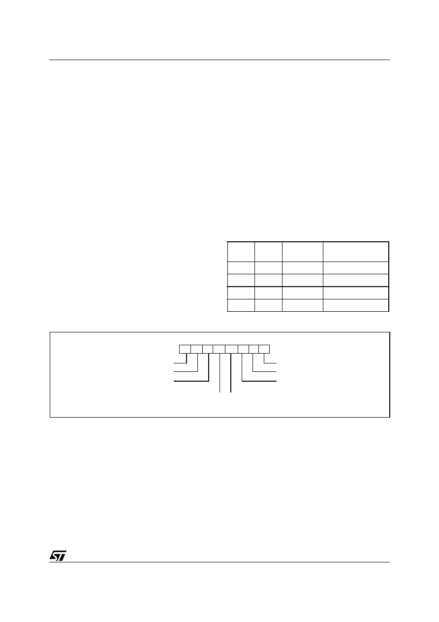
Table 4. .Register Bank Select Addresses
Figure 12. Program Status Word (PSW) Register
RS1
RS0
Register
Bank
8032 Internal
DATA Address
0
0
0
00h - 07h
0
1
1
08h - 0Fh
1
0
2
10h - 17h
1
1
3
18h - 1Fh
AI06639
CY
Reset Value 00h
Parity Flag
Bit not assigned
Overflow Flag
Register Bank Select Flags
(to select Bank0-3)
Carry Flag
Auxillary Carry Flag
General Purpose Flag
AC FO RS1 RS0 OV
P
MSB
LSB
PSW

uPSD34xx - SPECIAL FUNCTION REGISTERS (SFR)
24/264
SPECIAL FUNCTION REGISTERS (SFR)
A group of registers designated as Special Func-
tion Register (SFR) is shown in
Table 5., page 25
.
SFRs control the operating modes of the MCU
core and also control the peripheral interfaces and
I/O pins on the MCU Module. The SFRs can be ac-
cessed only by using the Direct Addressing meth-
od within the address range from 80h to FFh of
internal 8032 SRAM. Sixteen addresses in SFR
address space are both byte- and bit-addressable.
The bit-addressable SFRs are noted in Table
5
.
106 of a possible 128 SFR addresses are occu-
pied. The remaining unoccupied SFR addresses
(designated as "RESERVED" in Table
5
) should
not be written. Reading unoccupied locations will
return an undefined value.
Note: There is a separate set of control registers
for the PSD Module, designated as csiop, and they
are described in the
PSD MODULE, page 164
.
The I/O pins, PLD, and other functions on the PSD
Module are NOT controlled by SFRs.
SFRs are categorized as follows:
MCU core registers:
IP, A, B, PSW, SP, DPTL, DPTH, DPTC,
DPTM
MCU Module I/O Port registers:
P1, P3, P4, P1SFS0, P1SFS1, P3SFS,
P4SFS0, P4SFS1
Standard 8032 Timer registers
TCON, TMOD, T2CON, TH0, TH1, TH2, TL0,
TL1, TL2, RCAP2L, RCAP2H
Standard Serial Interfaces (UART)
SCON0, SBUF0, SCON1, SBUF1
Power, clock, and bus timing registers
PCON, CCON0, CCON1, BUSCON
Hardware watchdog timer registers
WDKEY, WDRST
Interrupt system registers
IP, IPA, IE, IEA
Prog. Counter Array (PCA) control
registers
PCACL0, PCACH0, PCACON0, PCASTA,
PCACL1, PCACH1, PCACON1, CCON2,
CCON3
PCA capture/compare and PWM registers
CAPCOML0, CAPCOMH0, TCMMODE0,
CAPCOML1, CAPCOMH1, TCMMODE2,
CAPCOML2, CAPCOMH2, TCMMODE2,
CAPCOML3, CAPCOMH3, TCMMODE3,
CAPCOML4, CAPCOMH4, TCMMODE4,
CAPCOML5, CAPCOMH5, TCMMODE5,
PWMF0, PMWF1
SPI interface registers
SPICLKD, SPISTAT, SPITDR, SPIRDR,
SPICON0, SPICON1
I
2
C interface registers
S1SETUP, S1CON, S1STA, S1DAT, S1ADR
Analog to Digital Converter registers
ACON, ADCPS, ADAT0, ADAT1
IrDA interface register
IRDACON
USB interface registers
UADDR, UPAIR, WE0-3, UIF0-3, UCTL,
USTA, USEL, UCON, USIZE, UBASEH,
UBASEL, USCI, USCV

25/264
uPSD34xx - SPECIAL FUNCTION REGISTERS (SFR)
Table 5. SFR Memory Map with Direct Address and Reset Value
SFR
Addr
(hex)
SFR
Name
Bit Name and <Bit Address>
Reset
Value
(hex)
Reg.
Descr.
with Link
7
6
5
4
3
2
1
0
80
RESERVED
81
SP
SP[7:0]
07
Stack
Pointer
(SP), page
22
82
DPL
DPL[7:0]
00
Data
Pointer
(DPTR), p
age 22
83
DPH
DPH[7:0]
00
84
RESERVED
85
DPTC
≠
AT
≠
≠
≠
DPSEL[2:0]
00
Table
13., page
38
86
DPTM
≠
≠
≠
≠
MD1[1:0]
MD0[1:0]
00
Table
14., page
39
87
PCON
SMOD0 SMOD1
≠
POR
RCLK1
TCLK1
PD
IDLE
00
Table
26., page
52
88
(1)
TCON
TF1
<8Fh>
TR1
<8Eh>
TF0
<8Dh>
TR0
<8Ch>
IE1
<8Bh>
IT1
<8Ah>
IE0
<89h>
IT0
<88h>
00
Table
41., page
72
89
TMOD
GATE
C/T
M1
M0
GATE
C/T
M1
M0
00
Table
42., page
74
8A
TL0
TL0[7:0]
00
Standard
Timer
SFRs, pag
e 71
8B
TL1
TL1[7:0]
00
8C
TH0
TH0[7:0]
00
8D
TH1
TH1[7:0]
00
8E
P1SFS0
P1SFS0[7:0]
00
Table
31., page
61
8F
P1SFS1
P1SFS1[7:0]
00
Table
32., page
61
90
(1)
P1
P1.7
<97h>
P1.6
<96h>
P1.5
<95h>
P1.4
<94h>
P1.3
<93h>
P1.2
<92h>
P1.1
<91h>
P1.0
<90h>
FF
Table
27., page
58
91
P3SFS
P3SFS[7:0]
00
Table
30., page
61
92
P4SFS0
P4SFS0[7:0]
00
Table
34., page
62
93
P4SFS1
P4SFS1[7:0]
00
Table
35., page
62
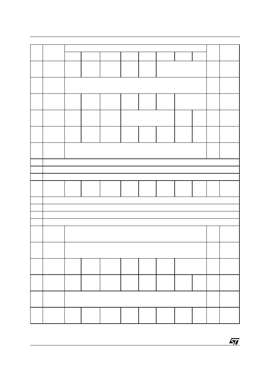
uPSD34xx - SPECIAL FUNCTION REGISTERS (SFR)
26/264
94
ADCPS
≠
≠
≠
≠
ADCCE
ADCPS[2:0]
00
Table
90., page
153
95
ADAT0
ADATA[7:0]
00
Table
91., page
153
96
ADAT1
≠
≠
≠
≠
≠
≠
ADATA[9:8]
00
Table
92., page
153
97
ACON
AINTF
AINTEN
ADEN
ADS[2:0]
ADST
ADSF
00
Table
89., page
152
98
(1)
SCON0
SM0
<9Fh>
SM1
<9Eh>
SM2
<9Dh>
REN
<9Ch>
TB8
<9Bh>
RB8
<9Ah>
TI
<99h>
RI
<9h8>
00
Table
47., page
84
99
SBUF0
SBUF0[7:0]
00
Figure
28., page
81
9A
RESERVED
9B
RESERVED
9C
RESERVED
9D
BUSCON
EPFQ
EBC
WRW1
WRW0
RDW1
RDW0
CW1
CW0
EB
Table
37., page
65
9E
RESERVED
9F
RESERVED
A0
RESERVED
A1
RESERVED
A2
PCACL0
PCACL0[7:0]
00
Table
93., page
155
A3
PCACH0
PCACH0[7:0]
00
Table
93., page
155
A4
PCACON0 EN_ALL EN_PCA
EOVF1
PCA_IDL
≠
≠
CLK_SEL[1:0]
00
Table
96., page
160
A5
PCASTA
OVF1
INTF5
INTF4
INTF3
OVF0
INTF2
INTF1
INTF0
00
Table
98., page
162
A6
WDRST
WDRST[7:0]
00
Table
40., page
70
A7
IEA
EADC
ESPI
EPCA
ES1
≠
≠
EI2C
≠
00
Table
18., page
45
SFR
Addr
(hex)
SFR
Name
Bit Name and <Bit Address>
Reset
Value
(hex)
Reg.
Descr.
with Link
7
6
5
4
3
2
1
0

27/264
uPSD34xx - SPECIAL FUNCTION REGISTERS (SFR)
A8
(1)
IE
EA
<AFh>
≠
ET2
<ADh>
ES0
<ACh>
ET1
<ABh>
EX1
<AAh>
ET0
<A9h>
EX0
<A8h>
00
Table
17., page
45
A9
TCMMODE
0
EINTF E_COMP
CAP_PE CAP_NE MATCH TOGGLE
PWM[1:0]
00
Table
99., page
163
AA
TCMMODE
1
EINTF E_COMP
CAP_PE CAP_NE MATCH TOGGLE
PWM[1:0]
00
AB
TCMMODE
2
EINTF E_COMP
CAP_PE CAP_NE MATCH TOGGLE
PWM[1:0]
00
AC
CAPCOML
0
CAPCOML0[7:0]
00
Table
93., page
155
AD
CAPCOMH
0
CAPCOMH0[7:0]
00
AE
WDKEY
WDKEY[7:0]
55
Table
39., page
70
AF
CAPCOML
1
CAPCOML1[7:0]
00
Table
93., page
155
B0
(1)
P3
P3.7
<B7h>
P3.6
<B6h>
P3.5
<B5h>
P3.4
<B4h>
P3.3
<B3h>
P3.2
<B2h>
P3.1
<B1h>
P3.0
<B0h>
FF
Table
28., page
59
B1
CAPCOMH
1
CAPCOMH1[7:0]
00
Table
93., page
155
B2
CAPCOML
2
CAPCOML2[7:0]
00
B3
CAPCOMH
2
CAPCOMH2[7:0]
00
B4
PWMF0
PWMF0[7:0]
00
B5
RESERVED
B6
RESERVED
B7
IPA
PADC
PSPI
PPCA
PS1
≠
≠
PI2C
≠
00
Table
20., page
46
B8
(1)
IP
≠
≠
PT2
<BDh>
PS0
<BCh>
PT1
<BBh>
PX1
<BAh>
PT0
<B9h>
PX0
<B8h>
00
Table
19., page
46
B9
RESERVED
BA
PCACL1
PCACL1[7:0]
00
Table
93., page
155
BB
PCACH1
PCACH1[7:0]
00
BC
PCACON1
≠
EN_PCA
EOVF1
PCA_IDL
≠
≠
CLK_SEL[1:0]
00
Table
97., page
161
SFR
Addr
(hex)
SFR
Name
Bit Name and <Bit Address>
Reset
Value
(hex)
Reg.
Descr.
with Link
7
6
5
4
3
2
1
0

uPSD34xx - SPECIAL FUNCTION REGISTERS (SFR)
28/264
BD
TCMMODE
3
EINTF E_COMP
CAP_PE CAP_NE MATCH TOGGLE
PWM[1:0]
00
Table
99., page
163
BE
TCMMODE
4
EINTF E_COMP
CAP_PE CAP_NE MATCH TOGGLE
PWM[1:0]
00
BF
TCMMODE
5
EINTF E_COMP
CAP_PE CAP_NE MATCH TOGGLE
PWM[1:0]
00
C0
(1)
P4
P4.7
<C7h>
P4.6
<C6h>
P4.5
<C5h>
P4.4
<C4h>
P4.3
<C3h>
P4.2
<C2h>
P4.1
<C1h>
P4.0
<C0h>
FF
Table
29., page
59
C1
CAPCOML
3
CAPCOML3[7:0]
00
Table
93., page
155
C2
CAPCOMH
3
CAPCOMH3[7:0]
00
C3
CAPCOML
4
CAPCOML4[7:0]
00
C4
CAPCOMH
4
CAPCOMH4[7:0]
00
C5
CAPCOML
5
CAPCOML5[7:0]
00
C6
CAPCOMH
5
CAPCOMH5[7:0]
00
C7
PWMF1
PWMF1[7:0]
00
C8
(1)
T2CON
TF2
<CFh>
EXF2
<CEh>
RCLK
<CDh>
TCLK
<CCh>
EXEN2
<CBh>
TR2
<CAh>
C/T2
<C9h>
CP/
RL2
<C8h>
00
Table
43., page
77
C9
RESERVED
CA
RCAP2L
RCAP2L[7:0]
00
Standard
Timer
SFRs, pag
e 71
CB
RCAP2H
RCAP2H[7:0]
00
CC
TL2
TL2[7:0]
00
CD
TH2
TH2[7:0]
00
CE
IRDACON
≠
IRDA_EN BIT_PULS
CDIV4
CDIV3
CDIV2
CDIV1
CDIV0
0F
Table
50., page
95
D0
(1)
PSW
CY
<D7h>
AC
<D6h>
F0
<D5h>
RS[1:0]
<D4h, D3h>
OV
<D2h>
≠
P
<D0>
00
Program
Status
Word
(PSW), pa
ge 23
D1
RESERVED
D2
SPICLKD
SPICLKD[5:0]
≠
≠
04
Table
65., page
121
D3
SPISTAT
≠
≠
≠
BUSY
TEISF
RORISF
TISF
RISF
02
Table
66., page
122
SFR
Addr
(hex)
SFR
Name
Bit Name and <Bit Address>
Reset
Value
(hex)
Reg.
Descr.
with Link
7
6
5
4
3
2
1
0
29/264
uPSD34xx - SPECIAL FUNCTION REGISTERS (SFR)
D4
SPITDR
SPITDR[7:0]
00
Table
64., page
121
D5
SPIRDR
SPIRDR[7:0]
00
D6
SPICON0
≠
TE
RE
SPIEN
SSEL
FLSB
SPO
≠
00
Table
63., page
120
D7
SPICON1
≠
≠
≠
≠
TEIE
RORIE
TIE
RIE
00
Table
64., page
121
D8
(1)
SCON1
SM0
<DF
SM1
<DE>
SM2
<DD>
REN
<DC>
TB8
<DB>
RB8
<DA>
TI
<D9>
RI
<D8>
00
Table
48., page
85
D9
SBUF1
SBUF1[7:0]
00
Figure
28., page
81
DA
RESERVED
DB
S1SETUP SS_EN
SMPL_SET[6:0]
00
Table
59., page
108
DC
S1CON
CR2
EN1
STA
STO
ADDR
AA
CR1
CR0
00
Table
54., page
103
DD
S1STA
GC
STOP
INTR
TX_MD B_BUSY B_LOST
ACK_R
SLV
00
Table
56., page
106
DE
S1DAT
S1DAT[7:0]
00
Table
57., page
107
DF
S1ADR
S1ADR[7:0]
00
Table
58., page
107
E0
(1)
A
A[7:0]
<bit addresses: E7h, E6h, E5h, E4h, E3h, E2h, E1h, E0h>
00
Accumulat
or
(ACC), pa
ge 22
E1
RESERVED
E2
UADDR
≠
USBADDR[6:0]
00
E3
UPAIR
≠
≠
≠
≠
PR3OUT PR1OUT
PR3IN
PR1IN
00
E4
UIE0
≠
≠
≠
≠
RSTIE
SUSPND
IE
EOPIE
RES
UMIE
00
E5
UIE1
≠
≠
≠
IN4IE
IN3IE
IN2IE
IN1IE
IN0IE
00
E6
UIE2
≠
≠
≠
OUT4IE OUT3IE
OUT2IE
OUT1IE
OUT0I
E
00
E7
UIE3
≠
≠
≠
NAK4IE NAK3IE
NAK2IE
NAK1IE
NAK0I
E
00
E8
UIF0
GLF
INF
OUTF
NAKF
RSTF
SUSPND
F
EOPF
RESU
MF
00
SFR
Addr
(hex)
SFR
Name
Bit Name and <Bit Address>
Reset
Value
(hex)
Reg.
Descr.
with Link
7
6
5
4
3
2
1
0

uPSD34xx - SPECIAL FUNCTION REGISTERS (SFR)
30/264
Note: 1. This SFR can be addressed by individual bits (Bit Address mode) or addressed by the entire byte (Direct Address mode).
E9
UIF1
≠
≠
≠
IN4F
IN3F
IN2F
IN1F
IN0F
00
EA
UIF2
≠
≠
≠
OUT4F
OUT3F
OUT2F
OUT1F OUT0F
00
EB
UIF3
≠
≠
≠
NAK4F
NAK3F
NAK2F
NAK1F NAK0F
00
EC
UCTL
≠
≠
≠
≠
≠
USBEN
VISIBLE
WAKE
UP
00
ED
USTA
≠
≠
≠
≠
RCVT
SETUP
IN
OUT
00
EE
RESERVED
EF
USEL
DIR
≠
≠
≠
≠
EP[2:0]
00
F0
(1)
B
B[7:0]
<bit addresses: F7h, F6h, F5h, F4h, F3h, F2h, F1h, F0h>
00
B Register
(B), page
22
F1
UCON
≠
≠
≠
≠
ENABLE
STALL
TOGGLE
BSY
00
F2
USIZE
≠
SIZE[6:0]
00
F3
UBASEH
BASEADDR[15:8]
00
F4
UBASEL
BASEADDR[7:6]
0
0
0
0
0
0
00
F5
USCI
≠
≠
≠
≠
≠
USCI[2:0]
00
F6
USCV
USCV[7:0]
00
F7
RESERVED
F8
RESERVED
F9
CCON0
PLLM[4]
PLLEN
UPLLCE
DBGCE
CPU_
AR
CPUPS[2:0]
50
Table
22., page
49
FA
CCON1
PLLM[3:0]
PLLD[3:0]
00
FB
CCON2
≠
≠
≠
PCA0CE
PCA0PS[3:0]
10
Table
94., page
156
FC
CCON3
≠
≠
≠
PCA1CE
PCA1PS[3:0]
10
Table
95., page
156
FD
RESERVED
FE
RESERVED
FF
RESERVED
FE
RESERVED
FF
RESERVED
SFR
Addr
(hex)
SFR
Name
Bit Name and <Bit Address>
Reset
Value
(hex)
Reg.
Descr.
with Link
7
6
5
4
3
2
1
0

31/264
uPSD34xx - 8032 ADDRESSING MODES
8032 ADDRESSING MODES
The 8032 MCU uses 11 different addressing
modes listed below:
Register
Direct
Register Indirect
Immediate
External Direct
External Indirect
Indexed
Relative
Absolute
Long
Bit
Register Addressing
This mode uses the contents of one of the regis-
ters R0 - R7 (selected by the last three bits in the
instruction opcode) as the operand source or des-
tination. This mode is very efficient since an addi-
tional instruction byte is not needed to identify the
operand. For example:
Direct Addressing
This mode uses an 8-bit address, which is con-
tained in the second byte of the instruction, to di-
rectly address an operand which resides in either
8032 DATA SRAM (internal address range 00h-
07Fh) or resides in 8032 SFR (internal address
range 80h-FFh). This mode is quite fast since the
range limit is 256 bytes of internal 8032 SRAM.
For example:
Register Indirect Addressing
This mode uses an 8-bit address contained in ei-
ther Register R0 or R1 to indirectly address an op-
erand which resides in 8032 IDATA SRAM
(internal address range 80h-FFh). Although 8032
SFR registers also occupy the same physical ad-
dress range as IDATA, SFRs will not be accessed
by Register Indirect mode. SFRs may only be ac-
cesses using Direct address mode. For example:
Immediate Addressing
This mode uses 8-bits of data (a constant) con-
tained in the second byte of the instruction, and
stores it into the memory location or register indi-
cated by the first byte of the instruction. Thus, the
data is immediately available within the instruction.
This mode is commonly used to initialize registers
and SFRs or to perform mask operations.
There is also a 16-bit version of this mode for load-
ing the DPTR Register. In this case, the two bytes
following the instruction byte contain the 16-bit val-
ue. For example:
External Direct Addressing
This mode will access external memory (XDATA)
by using the 16-bit address stored in the DPTR
Register. There are only two instructions using this
mode and both use the accumulator to either re-
ceive a byte from external memory addressed by
DPTR or to send a byte from the accumulator to
the address in DPTR. The uPSD34xx has a spe-
cial feature to alternate the contents (source and
destination) of DPTR rapidly to implement very ef-
ficient memory-to-memory transfers. For example:
Note: See details in
DUAL DATA
POINTERS, page 38
.
External Indirect Addressing
This mode will access external memory (XDATA)
by using the 8-bit address stored in either Register
R0 or R1. This is the fastest way to access XDATA
(least bus cycles), but because only 8-bits are
available for address, this mode limits XDATA to a
size of only 256 bytes (the traditional Port 2 of the
8032 MCU is not available in the uPSD34xx, so it
is not possible to write the upper address byte).
This mode is not supported by uPSD34xx.
For example:
MOV A, R7
; Move contents of R7 to accumulator
MOV A, 40h
; Move contents of DATA SRAM
; at location 40h into the accumulator
MOV A, @R0
; Move into the accumulator the
; contents of IDATA SRAM that is
; pointed to by the address
; contained in R0.
MOV A, 40#
; Move the constant, 40h, into
; the accumulator
MOV DPTR, 1234# ; Move the constant, 1234h, into
; DPTR
MOVX A, @DPTR ; Move contents of accumulator to
; XDATA at address contained in
; DPTR
MOVX @DPTR, A ; Move XDATA to accumulator
MOVX @R0,A
; Move into the accumulator the
; XDATA that is pointed to by
; the address contained in R0.

uPSD34xx - 8032 ADDRESSING MODES
32/264
Indexed Addressing
This mode is used for the MOVC instruction which
allows the 8032 to read a constant from program
memory (not data memory). MOVC is often used
to read look-up tables that are embedded in pro-
gram memory. The final address produced by this
mode is the result of adding either the 16-bit PC or
DPTR value to the contents of the accumulator.
The value in the accumulator is referred to as an
index. The data fetched from the final location in
program memory is stored into the accumulator,
overwriting the index value that was previously
stored there. For example:
Relative Addressing
This mode will add the two's-compliment number
stored in the second byte of the instruction to the
program counter for short jumps within +128 or ≠
127 addresses relative to the program counter.
This is commonly used for looping and is very effi-
cient since no additional bus cycle is needed to
fetch the jump destination address. For example:
Absolute Addressing
This mode will append the 5 high-order bits of the
address of the next instruction to the 11 low-order
bits of an ACALL or AJUMP instruction to produce
a 16-bit jump address. The jump will be within the
same 2K byte page of program memory as the first
byte of the following instruction. For example:
Long Addressing
This mode will use the 16-bits contained in the two
bytes following the instruction byte as a jump des-
tination address for LCALL and LJMP instructions.
For example:
Bit Addressing
This mode allows setting or clearing an individual
bit without disturbing the other bits within an 8-bit
value of internal SRAM. Bit Addressing is only
available for certain locations in 8032 DATA and
SFR memory. Valid locations are DATA address-
es 20h - 2Fh and for SFR addresses whose base
address ends with 0h or 8h. (Example: The SFR,
IE, has a base address of A8h, so each of the eight
bits in IE can be addressed individually at address
A8h, A9h, ...up to AFh.) For example:
MOVC A, @A+DPTR; Move code byte relative to
; DPTR into accumulator
MOVC A, @A+PC
; Move code byte relative to PC
; into accumulator
SJMP 34h
; Jump 34h bytes ahead (in program
; memory) of the address at which
; the SJMP instruction is stored. If
; SJMP is at 1000h, program
; execution jumps to 1034h.
AJMP 0500h
; If next instruction is located at
; address 4000h, the resulting jump
; will be made to 4500h.
LJMP 0500h
; Unconditionally jump to address
; 0500h in program memory
SETB AFh
; Set the individual EA bit (Enable All
; Interrupts) inside the SFR Register,
; IE.

33/264
uPSD34xx - uPSD34xx INSTRUCTION SET SUMMARY
uPSD34xx INSTRUCTION SET SUMMARY
Tables
6
through
11
list all of the instructions sup-
ported by the uPSD34xx, including the number of
bytes and number of machine cycles required to
implement each instruction. This is the standard
8051 instruction set.
The meaning of "machine cycles" is how many
8032 MCU core machine cycles are required to
execute the instruction. The "native" duration of all
machine cycles is set by the memory wait state
settings in the SFR, BUSCON, and the MCU clock
divider selections in the SFR, CCON0 (i.e. a ma-
chine cycle is typically set to 4 MCU clocks for a 5V
uPSD34xx). However, an individual machine cycle
may grow in duration when either of two things
happen:
1.
a stall is imposed while loading the 8032 Pre-
Fetch Queue (PFQ); or
2.
the occurrence of a cache miss in the Branch
Cache (BC) during a branch in program
execution flow.
See
8032 MCU CORE PERFORMANCE
ENHANCEMENTS, page 18
or more details.
But generally speaking, during typical program ex-
ecution, the PFQ is not empty and the BC has no
misses, producing very good performance without
extending the duration of any machine cycles.
The uPSD34xx Programmers Guide describes
each instruction operation in detail.
Table 6. Arithmetic Instruction Set
Note: 1. All mnemonics copyrighted ©Intel Corporation 1980.
Mnemonic
(1)
and Use
Description
Length/Cycles
ADD
A, Rn
Add register to ACC
1 byte/1 cycle
ADD
A, Direct
Add direct byte to ACC
2 byte/1 cycle
ADD
A, @Ri
Add indirect SRAM to ACC
1 byte/1 cycle
ADD
A, #data
Add immediate data to ACC
2 byte/1 cycle
ADDC
A, Rn
Add register to ACC with carry
1 byte/1 cycle
ADDC
A, direct
Add direct byte to ACC with carry
2 byte/1 cycle
ADDC
A, @Ri
Add indirect SRAM to ACC with carry
1 byte/1 cycle
ADDC
A, #data
Add immediate data to ACC with carry
2 byte/1 cycle
SUBB
A, Rn
Subtract register from ACC with borrow
1 byte/1 cycle
SUBB
A, direct
Subtract direct byte from ACC with borrow
2 byte/1 cycle
SUBB
A, @Ri
Subtract indirect SRAM from ACC with borrow
1 byte/1 cycle
SUBB
A, #data
Subtract immediate data from ACC with borrow
2 byte/1 cycle
INC
A
Increment A
1 byte/1 cycle
INC
Rn
Increment register
1 byte/1 cycle
INC
direct
Increment direct byte
2 byte/1 cycle
INC
@Ri
Increment indirect SRAM
1 byte/1 cycle
DEC
A
Decrement ACC
1 byte/1 cycle
DEC
Rn
Decrement register
1 byte/1 cycle
DEC
direct
Decrement direct byte
2 byte/1 cycle
DEC
@Ri
Decrement indirect SRAM
1 byte/1 cycle
INC
DPTR
Increment Data Pointer
1 byte/2 cycle
MUL
AB
Multiply ACC and B
1 byte/4 cycle
DIV
AB
Divide ACC by B
1 byte/4 cycle
DA
A
Decimal adjust ACC
1 byte/1 cycle

uPSD34xx - uPSD34xx INSTRUCTION SET SUMMARY
34/264
Table 7. Logical Instruction Set
Note: 1. All mnemonics copyrighted ©Intel Corporation 1980.
Mnemonic
(1)
and Use
Description
Length/Cycles
Logical Instructions
ANL
A, Rn
AND register to ACC
1 byte/1 cycle
ANL
A, direct
AND direct byte to ACC
2 byte/1 cycle
ANL
A, @Ri
AND indirect SRAM to ACC
1 byte/1 cycle
ANL
A, #data
AND immediate data to ACC
2 byte/1 cycle
ANL
direct, A
AND ACC to direct byte
2 byte/1 cycle
ANL
direct, #data
AND immediate data to direct byte
3 byte/2 cycle
ORL
A, Rn
OR register to ACC
1 byte/1 cycle
ORL
A, direct
OR direct byte to ACC
2 byte/1 cycle
ORL
A, @Ri
OR indirect SRAM to ACC
1 byte/1 cycle
ORL
A, #data
OR immediate data to ACC
2 byte/1 cycle
ORL
direct, A
OR ACC to direct byte
2 byte/1 cycle
ORL
direct, #data
OR immediate data to direct byte
3 byte/2 cycle
SWAP
A
Swap nibbles within the ACC
1 byte/1 cycle
XRL
A, Rn
Exclusive-OR register to ACC
1 byte/1 cycle
XRL
A, direct
Exclusive-OR direct byte to ACC
2 byte/1 cycle
XRL
A, @Ri
Exclusive-OR indirect SRAM to ACC
1 byte/1 cycle
XRL
A, #data
Exclusive-OR immediate data to ACC
2 byte/1 cycle
XRL
direct, A
Exclusive-OR ACC to direct byte
2 byte/1 cycle
XRL
direct, #data
Exclusive-OR immediate data to direct byte
3 byte/2 cycle
CLR
A
Clear ACC
1 byte/1 cycle
CPL
A
Compliment ACC
1 byte/1 cycle
RL
A
Rotate ACC left
1 byte/1 cycle
RLC
A
Rotate ACC left through the carry
1 byte/1 cycle
RR
A
Rotate ACC right
1 byte/1 cycle
RRC
A
Rotate ACC right through the carry
1 byte/1 cycle

35/264
uPSD34xx - uPSD34xx INSTRUCTION SET SUMMARY
Table 8. Data Transfer Instruction Set
Note: 1. All mnemonics copyrighted ©Intel Corporation 1980.
Mnemonic
(1)
and Use
Description
Length/Cycles
MOV
A, Rn
Move register to ACC
1 byte/1 cycle
MOV
A, direct
Move direct byte to ACC
2 byte/1 cycle
MOV
A, @Ri
Move indirect SRAM to ACC
1 byte/1 cycle
MOV
A, #data
Move immediate data to ACC
2 byte/1 cycle
MOV
Rn, A
Move ACC to register
1 byte/1 cycle
MOV
Rn, direct
Move direct byte to register
2 byte/2 cycle
MOV
Rn, #data
Move immediate data to register
2 byte/1 cycle
MOV
direct, A
Move ACC to direct byte
2 byte/1 cycle
MOV
direct, Rn
Move register to direct byte
2 byte/2 cycle
MOV
direct, direct
Move direct byte to direct
3 byte/2 cycle
MOV
direct, @Ri
Move indirect SRAM to direct byte
2 byte/2 cycle
MOV
direct, #data
Move immediate data to direct byte
3 byte/2 cycle
MOV
@Ri, A
Move ACC to indirect SRAM
1 byte/1 cycle
MOV
@Ri, direct
Move direct byte to indirect SRAM
2 byte/2 cycle
MOV
@Ri, #data
Move immediate data to indirect SRAM
2 byte/1 cycle
MOV
DPTR, #data16
Load Data Pointer with 16-bit constant
3 byte/2 cycle
MOVC
A, @A+DPTR
Move code byte relative to DPTR to ACC
1 byte/2 cycle
MOVC
A, @A+PC
Move code byte relative to PC to ACC
1 byte/2 cycle
MOVX
A, @Ri
Move XDATA (8-bit addr) to ACC
1 byte/2 cycle
MOVX
A, @DPTR
Move XDATA (16-bit addr) to ACC
1 byte/2 cycle
MOVX
@Ri, A
Move ACC to XDATA (8-bit addr)
1 byte/2 cycle
MOVX
@DPTR, A
Move ACC to XDATA (16-bit addr)
1 byte/2 cycle
XCH
A, Rn
Exchange register with ACC
1 byte/1 cycle
PUSH
direct
Push direct byte onto stack
2 byte/2 cycle
POP
direct
Pop direct byte from stack
2 byte/2 cycle
XCH
A, direct
Exchange direct byte with ACC
2 byte/1 cycle
XCH
A, @Ri
Exchange indirect SRAM with ACC
1 byte/1 cycle
XCHD
A, @Ri
Exchange low-order digit indirect SRAM with ACC
1 byte/1 cycle

uPSD34xx - uPSD34xx INSTRUCTION SET SUMMARY
36/264
Table 9. Boolean Variable Manipulation Instruction Set
Note: 1. All mnemonics copyrighted ©Intel Corporation 1980.
Mnemonic
(1)
and Use
Description
Length/Cycles
CLR
C
Clear carry
1 byte/1 cycle
CLR
bit
Clear direct bit
2 byte/1 cycle
SETB
C
Set carry
1 byte/1 cycle
SETB
bit
Set direct bit
2 byte/1 cycle
CPL
C
Compliment carry
1 byte/1 cycle
CPL
bit
Compliment direct bit
2 byte/1 cycle
ANL
C, bit
AND direct bit to carry
2 byte/2 cycle
ANL
C, /bit
AND compliment of direct bit to carry
2 byte/2 cycle
ORL
C, bit
OR direct bit to carry
2 byte/2 cycle
ORL
C, /bit
OR compliment of direct bit to carry
2 byte/2 cycle
MOV
C, bit
Move direct bit to carry
2 byte/1 cycle
MOV
bit, C
Move carry to direct bit
2 byte/2 cycle
JC
rel
Jump if carry is set
2 byte/2 cycle
JNC
rel
Jump if carry is not set
2 byte/2 cycle
JB
rel
Jump if direct bit is set
3 byte/2 cycle
JNB
rel
Jump if direct bit is not set
3 byte/2 cycle
JBC
bit, rel
Jump if direct bit is set and clear bit
3 byte/2 cycle
37/264
uPSD34xx - uPSD34xx INSTRUCTION SET SUMMARY
Table 10. Program Branching Instruction Set
Note: 1. All mnemonics copyrighted ©Intel Corporation 1980.
Table 11. Miscellaneous Instruction Set
Note: 1. All mnemonics copyrighted ©Intel Corporation 1980.
Table 12. Notes on Instruction Set and Addressing Modes
Mnemonic
(1)
and Use
Description
Length/Cycles
Program Branching Instructions
ACALL
addr11
Absolute subroutine call
2 byte/2 cycle
LCALL
addr16
Long subroutine call
3 byte/2 cycle
RET
Return from subroutine
1 byte/2 cycle
RETI
Return from interrupt
1 byte/2 cycle
AJMP
addr11
Absolute jump
2 byte/2 cycle
LJMP
addr16
Long jump
3 byte/2 cycle
SJMP
rel
Short jump (relative addr)
2 byte/2 cycle
JMP
@A+DPTR
Jump indirect relative to the DPTR
1 byte/2 cycle
JZ
rel
Jump if ACC is zero
2 byte/2 cycle
JNZ
rel
Jump if ACC is not zero
2 byte/2 cycle
CJNE
A, direct, rel
Compare direct byte to ACC, jump if not equal
3 byte/2 cycle
CJNE
A, #data, rel
Compare immediate to ACC, jump if not equal
3 byte/2 cycle
CJNE
Rn, #data, rel
Compare immediate to register, jump if not equal
3 byte/2 cycle
CJNE
@Ri, #data, rel
Compare immediate to indirect, jump if not equal
3 byte/2 cycle
DJNZ
Rn, rel
Decrement register and jump if not zero
2 byte/2 cycle
DJNZ
direct, rel
Decrement direct byte and jump if not zero
3 byte/2 cycle
Mnemonic
(1)
and Use
Description
Length/Cycles
Miscellaneous
NOP
No Operation
1 byte/1 cycle
Rn
Register R0 - R7 of the currently selected register bank.
direct
8-bit address for internal 8032 DATA SRAM (locations 00h - 7Fh) or SFR registers (locations 80h - FFh).
@Ri
8-bit internal 8032 SRAM (locations 00h - FFh) addressed indirectly through contents of R0 or R1.
#data
8-bit constant included within the instruction.
#data16
16-bit constant included within the instruction.
addr16
16-bit destination address used by LCALL and LJMP.
addr11
11-bit destination address used by ACALL and AJMP.
rel
Signed (two-s compliment) 8-bit offset byte.
bit
Direct addressed bit in internal 8032 DATA SRAM (locations 20h to 2Fh) or in SFR registers (88h, 90h,
98h, A8h, B0, B8h, C0h, C8h, D0h, D8h, E0h, F0h).
uPSD34xx - DUAL DATA POINTERS
38/264
DUAL DATA POINTERS
XDATA is accessed by the External Direct ad-
dressing mode, which uses a 16-bit address
stored in the DPTR Register. Traditional 8032 ar-
chitecture has only one DPTR Register. This is a
burden when transferring data between two XDA-
TA locations because it requires heavy use of the
working registers to manipulate the source and
destination pointers.
However, the uPSD34xx has two data pointers,
one for storing a source address and the other for
storing a destination address. These pointers can
be configured to automatically increment or decre-
ment after each data transfer, further reducing the
burden on the 8032 and making this kind of data
movement very efficient.
Data Pointer Control Register, DPTC (85h)
By default, the DPTR Register of the uPSD34xx
will behave no different than in a standard 8032
MCU. The DPSEL0 Bit of SFR register DPTC
shown in Table
13
, selects which one of the two
"background" data pointer registers (DPTR0 or
DPTR1) will function as the traditional DPTR Reg-
ister at any given time. After reset, the DPSEL0 Bit
is cleared, enabling DPTR0 to function as the DP-
TR, and firmware may access DPTR0 by reading
or writing the traditional DPTR Register at SFR ad-
dresses 82h and 83h. When the DPSEL0 bit is set,
then the DPTR1 Register functions as DPTR, and
firmware may now access DPTR1 through SFR
registers at 82h and 83h. The pointer which is not
selected by the DPSEL0 bit remains in the back-
ground and is not accessible by the 8032. If the
DPSEL0 bit is never set, then the uPSD34xx will
behave like a traditional 8032 having only one
DPTR Register.
To further speed XDATA to XDATA transfers, the
SFR bit, AT, may be set to automatically toggle the
two data pointers, DPTR0 and DPTR1, each time
the standard DPTR Register is accessed by a
MOVX instruction. This eliminates the need for
firmware to manually manipulate the DPSEL0 bit
between each data transfer.
Detailed description for the SFR register DPTC is
shown in Table
13
.
Table 13. DPTC: Data Pointer Control Register (SFR 85h, reset value 00h)
Bit 7
Bit 6
Bit 5
Bit 4
Bit 3
Bit 2
Bit 1
Bit 0
≠
AT
≠
≠
≠
≠
≠
DPSEL0
Details
Bit
Symbol
R/W
Definition
7
≠
≠
Reserved
6
AT
R,W
0 = Manually Select Data Pointer
1 = Auto Toggle between DPTR0 and DPTR1
5-1
≠
≠
Reserved
0
DPSE0
R,W
0 = DPTR0 Selected for use as DPTR
1 = DPTR1 Selected for use as DPTR
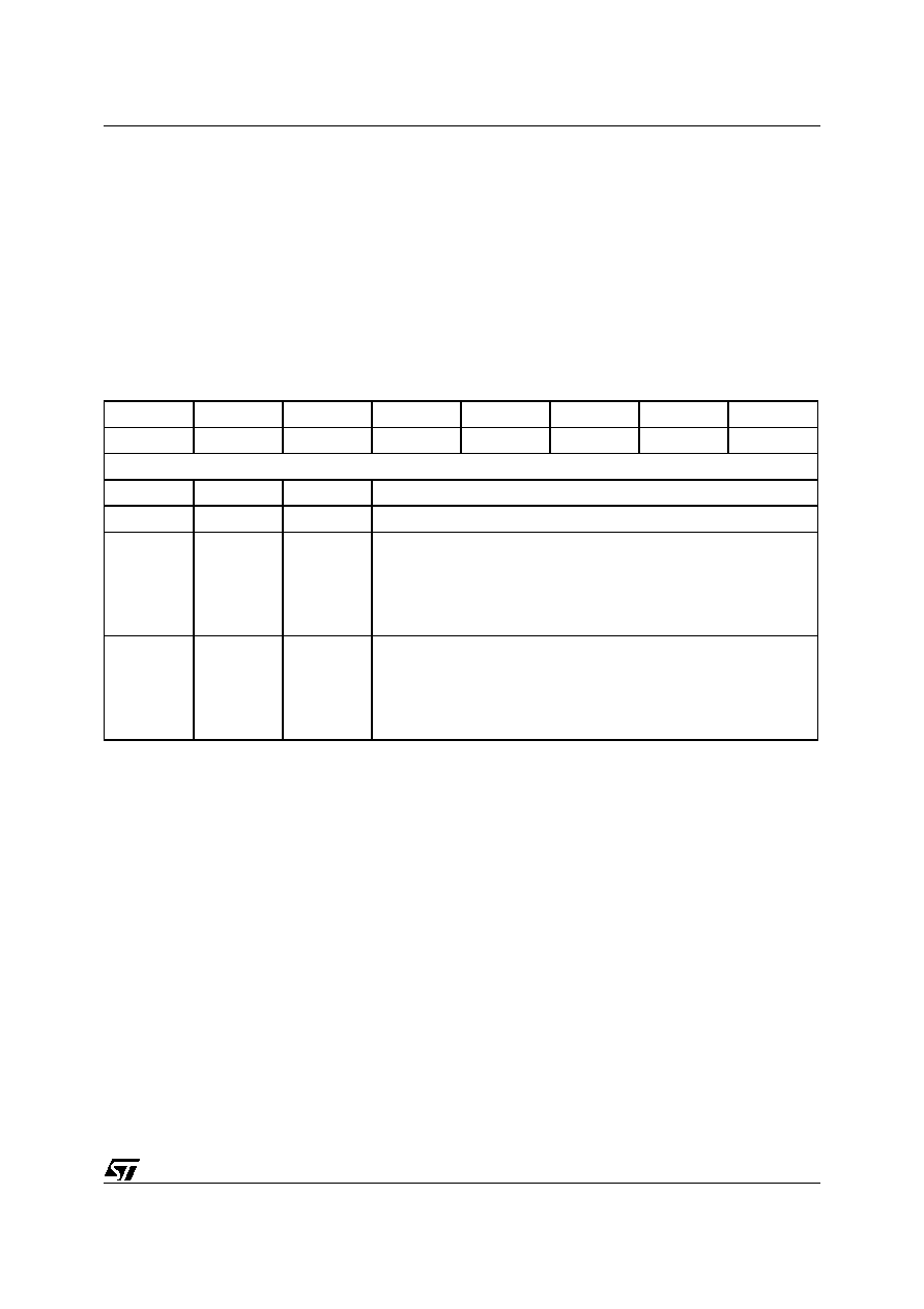
39/264
uPSD34xx - DUAL DATA POINTERS
Data Pointer Mode Register, DPTM (86h)
The two "background" data pointers, DPTR0 and
DPTR1, can be configured to automatically incre-
ment, decrement, or stay the same after a MOVX
instruction accesses the DPTR Register. Only the
currently selected pointer will be affected by the in-
crement or decrement. This feature is controlled
by the DPTM Register defined in Table
14
.
The automatic increment or decrement function is
effective only for the MOVX instruction, and not
MOVC or any other instruction that uses the DTPR
Register.
Firmware Example. The 8051 assembly code il-
lustrated in Table
15
shows how to transfer a block
of data bytes from one XDATA address region to
another XDATA address region. Auto-address in-
crementing and auto-pointer toggling will be used.
Table 14. DPTM: Data Pointer Mode Register (SFR 86h, reset value 00h)
Table 15. 8051 Assembly Code Example
Note: 1. The code loop where the data transfer takes place is only 3 lines of code.
Bit 7
Bit 6
Bit 5
Bit 4
Bit 3
Bit 2
Bit 1
Bit 0
≠
≠
≠
≠
MD11
MD10
MD01
MD00
Details
Bit
Symbol
R/W
Definition
7-4
≠
≠
Reserved
3-2
MD[11:10]
R,W
DPTR1 Mode Bits
00: DPTR1 No Change
01: Reserved
10: Auto Increment
11: Auto Decrement
1-0
MD[01:00]
R,W
DPTR0 Mode Bits
00: DPTR0 No Change
01: Reserved
10: Auto Increment
11: Auto Decrement
MOV
R7, #COUNT
; initialize size of data block to transfer
MOV
DPTR, #SOURCE_ADDR
; load XDATA source address base into DPTR0
MOV
85h, #01h
; load DPTC to access DPTR1 pointer
MOV
DPTR, #DEST_ADDR
; load XDATA destination address base into DPTR1
MOV
85h, #40h
; load DPTC to access DPTR0 pointer and auto toggle
MOV
86h, #0Ah
; load DPTM to auto-increment both pointers
LOOP:
MOVX
(1)
A, @DPTR
; load XDATA byte from source into ACC.
; after load completes, DPTR0 increments and DPTR
; switches DPTR1
MOVX
(1)
@DPTR, A
; store XDATA byte from ACC to destination.
; after store completes, DPTR1 increments and DPTR
; switches to DPTR0
DJNZ
(1)
R7, LOOP
; continue until done
MOV
86h, #00
; disable auto-increment
MOV
85h, #00
; disable auto-toggle, now back to single DPTR mode

uPSD34xx - DEBUG UNIT
40/264
DEBUG UNIT
The 8032 MCU Module supports run-time debug-
ging through the JTAG interface. This same JTAG
interface is also used for In-System Programming
(ISP) and the physical connections are described
in the PSD Module section,
JTAG ISP and JTAG
Debug, page 226
.
Debugging with a serial interface such as JTAG is
a non-intrusive way to gain access to the internal
state of the 8032 MCU core and various memo-
ries. A traditional external hardware emulator can-
not be completely effective on the uPSD34xx
because of the Pre-Fetch Queue and Branch
Cache. The nature of the PFQ and BC hide the
visibility of actual program flow through traditional
external bus connections, thus requiring on-chip
serial debugging instead.
Debugging is supported by Windows PC based
software tools used for 8051 code development
from 3rd party vendors listed at www.st.com/psm.
Debug capabilities include:
Halt or Start MCU execution
Reset the MCU
Single Step
3 Match Breakpoints
1 Range Breakpoint (inside or outside range)
Program Tracing
Read or Modify MCU core registers, DATA,
IDATA, SFR, XDATA, and Code
External Debug Event Pin, Input or Output
Some key points regarding use of the JTAG De-
bugger.
≠
The JTAG Debugger can access MCU
registers, data memory, and code memory
while the MCU is executing at full speed by
cycle-stealing. This means "watch windows"
may be displayed and periodically updated on
the PC during full speed operation. Registers
and data content may also be modified during
full speed operation.
≠
There is no on-chip storage for Program Trace
data, but instead this data is scanned from the
uPSD34xx through the JTAG channel at run-
time to the PC host for proccessing. As such,
full speed program tracing is possible only
when the 8032 MCU is operating below
approximately one MIPS of performance.
Above one MIPS, the program will not run
real-time while tracing. One MIPS
performance is determined by the
combination of choice for MCU clock
frequency, and the bit settings in SFR
registers BUSCON and CCON0.
≠
Breakpoints can optionally halt the MCU, and/
or assert the external Debug Event pin.
≠
Breakpoint definitions may be qualified with
read or write operations, and may also be
qualified with an address of code, SFR, DATA,
IDATA, or XDATA memories.
≠
Three breakpoints will compare an address,
but the fourth breakpoint can compare an
address and also data content. Additionally,
the fouth breakpoint can be logically combined
(AND/OR) with any of the other three
breakpoints.
≠
The Debug Event pin can be configured by the
PC host to generate an output pulse for
external triggering when a break condition is
met. The pin can also be configured as an
event input to the breakpoint logic, causing a
break on the falling-edge of an external event
signal. If not used, the Debug Event pin should
be pulled up to V
CC
as described in the
section,
Debugging the 8032 MCU
Module., page 232
.
≠
The duration of a pulse, generated when the
Event pin configured as an output, is one MCU
clock cycle. This is an active-low signal, so the
first edge when an event occurs is high-to-low.
≠
The clock to the Watchdog Timer, ADC, and
I
2
C interface are not stopped by a breakpoint
halt.
≠
The Watchdog Timer should be disabled while
debugging with JTAG, else a reset will be
generated upon a watchdog time-out.

41/264
uPSD34xx - INTERRUPT SYSTEM
INTERRUPT SYSTEM
The uPSD34xx has an 12-source, two priority level
interrupt structure summarized in Table
16
.
Firmware may assign each interrupt source either
high or low priority by writing to bits in the SFRs
named, IP and IPA, shown in Table
16
. An inter-
rupt will be serviced as long as an interrupt of
equal or higher priority is not already being ser-
viced. If an interrupt of equal or higher priority is
being serviced, the new interrupt will wait until it is
finished before being serviced. If a lower priority
interrupt is being serviced, it will be stopped and
the new interrupt is serviced. When the new inter-
rupt is finished, the lower priority interrupt that was
stopped will be completed. If new interrupt re-
quests are of the same priority level and are re-
ceived simultaneously, an internal polling
sequence determines which request is selected
for service. Thus, within each of the two priority
levels, there is a second priority structure deter-
mined by the polling sequence.
Firmware may individually enable or disable inter-
rupt sources by writing to bits in the SFRs named,
IE and IEA, shown in
Table 16., page 42
. The SFR
named IE contains a global disable bit (EA), which
can be cleared to disable all 12 interrupts at once,
as shown in
Table 17., page 45
.
Figure
13., page 43
illustrates the interrupt priority, poll-
ing, and enabling process.
Each interrupt source has at least one interrupt
flag that indicates whether or not an interrupt is
pending. These flags reside in bits of various
SFRs shown in
Table 16., page 42
.
All of the interrupt flags are latched into the inter-
rupt control system at the beginning of each MCU
machine cycle, and they are polled at the begin-
ning of the following machine cycle. If polling de-
termines one of the flags was set, the interrupt
control system automatically generates an LCALL
to the user's Interrupt Service Routine (ISR) firm-
ware stored in program memory at the appropriate
vector address.
The specific vector address for each of the inter-
rupt sources are listed in
Table 16., page 42
. How-
ever, this LCALL jump may be blocked by any of
the following conditions:
≠
An interrupt of equal or higher priority is
already in progress
≠
The current machine cycle is not the final cycle
in the execution of the instruction in progress
≠
The current instruction involves a write to any
of the SFRs: IE, IEA, IP, or IPA
≠
The current instruction is an RETI
Note: Interrupt flags are polled based on a sample
taken in the previous MCU machine cycle. If an in-
terrupt flag is active in one cycle but is denied ser-
viced due to the conditions above, and then later it
is not active when the conditions above are finally
satisfied, the previously denied interrupt will not be
serviced. This means that active interrupts are not
remembered. Every poling cycle is new.
Assuming all of the listed conditions are satisfied,
the MCU executes the hardware generated
LCALL to the appropriate ISR. This LCALL pushes
the contents of the PC onto the stack (but it does
not save the PSW) and loads the PC with the ap-
propriate interrupt vector address. Program exe-
cution then jumps to the ISR at the vector address.
Execution precedes in the ISR. It may be neces-
sary for the ISR firmware to clear the pending in-
terrupt flag for some interrupt sources, because
not all interrupt flags are automatically cleared by
hardware when the ISR is called, as shown in
Ta-
ble 16., page 42
. If an interrupt flag is not cleared
after servicing the interrupt, an unwanted interrupt
will occur upon exiting the ISR.
After the interrupt is serviced, the last instruction
executed by the ISR is RETI. The RETI informs
the MCU that the ISR is no longer in progress and
the MCU pops the top two bytes from the stack
and loads them into the PC. Execution of the inter-
rupted program continues where it left off.
Note: An ISR must end with a RETI instruction,
not a RET. An RET will not inform the interrupt
control system that the ISR is complete, leaving
the MCU to think the ISR is still in progress, mak-
ing future interrupts impossible.

uPSD34xx - INTERRUPT SYSTEM
42/264
Table 16. Interrupt Summary
Note: 1. See USB interrupt flag registers UIF0-3.
Interrupt
Source
Polling
Priority
Vector
Addr
Flag Bit Name
(SFR.bit position)
1 = Intr Pending
0 = No Interrupt
Flag Bit Auto-
Cleared
by Hardware?
Enable Bit Name
(SFR.bit position)
1 = Intr Enabled
0 = Intr Disabled
Priority Bit Name
(SFR.bit position)
1= High Priority
0 = Low Priority
Reserved
0 (high)
0063h
≠
≠
≠
≠
External
Interrupt INT0
1
0003h
IE0 (TCON.1)
Edge - Yes
Level - No
EX0 (IE.0)
PX0 (IP.0)
Timer 0
Overflow
2
000Bh
TF0 (TCON.5)
Yes
ET0 (IE.1)
PT0 (IP.1)
External
Interrupt INT1
3
0013h
IE1 (TCON.3
Edge - Yes
Level - No
EX1 (IE.2)
PX1 (IP.2)
Timer 1
Overflow
4
001Bh
TF1 (TCON.7)
Yes
ET1 (IE.3)
PT1 (IP.3)
UART0
5
0023h
RI (SCON0.0)
TI (SCON0.1)
No
ES0 (IE.4)
PS0 (IP.4)
Timer 2
Overflow
or TX2 Pin
6
002Bh
TF2 (T2CON.7)
EXF2 (T2CON.6)
No
ET2 (IE.5)
PT2 (IP.5)
SPI
7
0053h
TEISF, RORISF,
TISF, RISF
(SPISTAT[3:0])
Yes
ESPI (IEA.6)
PSPI (IPA.6)
USB
8
0033h
≠
(1)
No
EUSB (IEA.0)
PUSB (IPA.0)
I
2
C
9
0043h
INTR (S1STA.5)
Yes
EI
2
C (IEA.1)
PI
2
C (IPA.1)
ADC
10
003Bh
AINTF (ACON.7)
No
EADC (IEA.7)
PADC (IPA.7)
PCA
11
005Bh
OFVx, INTFx
(PCASTA[0:7])
No
EPCA (IEA.5)
PPCA (IPA.5)
UART1
12 (low)
004Bh
RI (SCON1.0)
TI (SCON1.1)
No
ES1 (IEA.4)
PS1 (IPA.4)

43/264
uPSD34xx - INTERRUPT SYSTEM
Figure 13. Enabling and Polling Interrupts
Reserved
Ext
INT0
Ext
INT1
Timer 0
UART0
Timer 1
SPI
USB
Timer 2
High
Low
Interr
upt P
olling
Sequence
Interrupt
Sources
IE/IEA
IP/IPA
Priority
Global
Enable
ADC
PCA
I
2
C
UART1
AI07844

uPSD34xx - INTERRUPT SYSTEM
44/264
Individual Interrupt Sources
External Interrupts Int0 and Int1. External in-
terrupt inputs on pins EXTINT0 and EXTINT1
(pins 3.2 and 3.3) are either edge-triggered or lev-
el-triggered, depending on bits IT0 and IT1 in the
SFR named TCON.
When an external interrupt is generated from an
edge-triggered (falling-edge) source, the appropri-
ate flag bit (IE0 or IE1) is automatically cleared by
hardware upon entering the ISR.
When an external interrupt is generated from a
level-triggered (low-level) source, the appropriate
flag bit (IE0 or IE1) is NOT automatically cleared
by hardware.
Timer 0 and 1 Overflow Interrupt. Timer 0 and
Timer 1 interrupts are generated by the flag bits
TF0 and TF1 when there is an overflow condition
in the respective Timer/Counter register (except
for Timer 0 in Mode 3).
Timer 2 Overflow Interrupt. This interrupt is
generated to the MCU by a logical OR of flag bits,
TF2 and EXE2. The ISR must read the flag bits to
determine the cause of the interrupt.
≠
TF2 is set by an overflow of Timer 2.
≠
EXE2 is generated by the falling edge of a
signal on the external pin, T2X (pin P1.1).
UART0 and UART1 Interrupt. Each of the
UARTs have identical interrupt structure. For each
UART, a single interrupt is generated to the MCU
by the logical OR of the flag bits, RI (byte received)
and TI (byte transmitted).
The ISR must read flag bits in the SFR named
SCON0 for UART0, or SCON1 for UART1 to de-
termine the cause of the interrupt.
SPI Interrupt. The SPI interrupt has four interrupt
sources, which are logically ORed together when
interrupting the MCU. The ISR must read the flag
bits to determine the cause of the interrupt.
A flag bit is set for: end of data transmit (TEISF);
data receive overrun (RORISF); transmit buffer
empty (TISF); or receive buffer full (RISF).
I
2
C Interrupt. The flag bit INTR is set by a variety
of conditions occurring on the I
2
C interface: re-
ceived own slave address (ADDR flag); received
general call address (GC flag); received STOP
condition (STOP flag); or successful transmission
or reception of a data byte.The ISR must read the
flag bits to determine the cause of the interrupt.
ADC Interrupt. The flag bit AINTF is set when an
A-to-D conversion has completed.
PCA Interrupt. The PCA has eight interrupt
sources, which are logically ORed together when
interrupting the MCU.The ISR must read the flag
bits to determine the cause of the interrupt.
≠
Each of the six TCMs can generate a "match
or capture" interrupt on flag bits OFV5..0
respectively.
≠
Each of the two 16-bit counters can generate
an overflow interrupt on flag bits INTF1 and
INTF0 respectively.
Tables
17
through
Table 20., page 46
have de-
tailed bit definitions of the interrupt system SFRs.
USB Interrupt. The USB interrupt has multiple
sources. The ISR must read the USB Interrupt
Flag Registers (UIF0-3) to determine the source of
the interrupt.
The USB interrupt can be activated by any of the
following four group of interrupt sources:
≠
Global: the interrupt flag is set when any of the
following events occurs: USB Reset, USB
Suspend, USB Resume, and End of Packet;
≠
In FIFO: the interrupt flag is set when any of
the End Point In FIFO becomes empty;
≠
Out FIFO: the interrupt flag is set when any of
the End Point Out FIFO becomes full; and
≠
In FIFO NAK: the interrupt flag is set when any
of the End Point In FIFO is not ready for an IN
(in-bound) packet.

45/264
uPSD34xx - INTERRUPT SYSTEM
Table 17. IE: Interrupt Enable Register (SFR A8h, reset value 00h)
Note: 1. 1 = Enable Interrupt, 0 = Disable Interrupt
Table 18. IEA: Interrupt Enable Addition Register (SFR A7h, reset value 00h)
Note: 1. 1 = Enable Interrupt, 0 = Disable Interrupt
Bit 7
Bit 6
Bit 5
Bit 4
Bit 3
Bit 2
Bit 1
Bit 0
EA
≠
ET2
ES0
ET1
EX1
ET0
EX0
Details
Bit
Symbol
R/W
Function
7
EA
R,W
Global disable bit. 0 = All interrupts are disabled. 1 = Each interrupt
source can be individually enabled or disabled by setting or clearing its
enable bit.
6
≠
R,W
Do not modify this bit. It is used by the JTAG debugger for instruction
tracing. Always read the bit and write back the same bit value when
writing this SFR.
5
(1)
ET2
R,W
Enable Timer 2 Interrupt
4
(1)
ES0
R,W
Enable UART0 Interrupt
3
(1)
ET1
R,W
Enable Timer 1 Interrupt
2
(1)
EX1
R,W
Enable External Interrupt INT1
1
(1)
ET0
R,W
Enable Timer 0 Interrupt
0
(1)
EX0
R,W
Enable External Interrupt INT0
Bit 7
Bit 6
Bit 5
Bit 4
Bit 3
Bit 2
Bit 1
Bit 0
EADC
ESPI
EPCA
ES1
≠
≠
EI
2
C
EUSB
Details
Bit
Symbol
R/W
Function
7
(1)
EADC
R,W
Enable ADC Interrupt
6
(1)
ESPI
R,W
Enable SPI Interrupt
5
(1)
EPCA
R,W
Enable Programmable Counter Array Interrupt
4
(1)
ES1
R,W
Enable UART1 Interrupt
3
≠
≠
Reserved, do not set to logic '1.'
2
≠
≠
Reserved, do not set to logic '1.'
1
(1)
EI
2
C
R,W
Enable I
2
C Interrupt
0
EUSB
R,W
Enable USB Interrupt
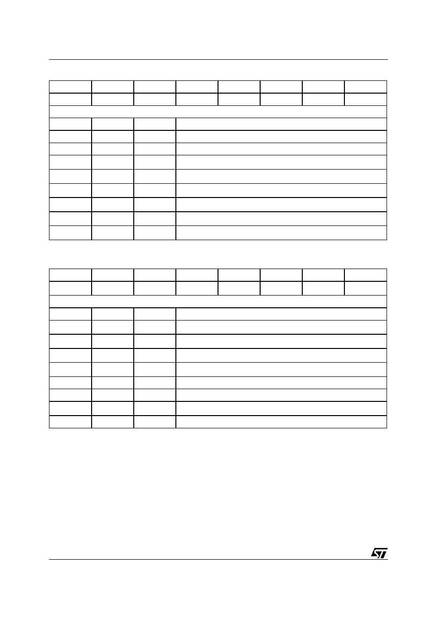
uPSD34xx - INTERRUPT SYSTEM
46/264
Table 19. IP: Interrupt Priority Register (SFR B8h, reset value 00h)
Note: 1. 1 = Assigns high priority level, 0 = Assigns low priority level
Table 20. IPA: Interrupt Priority Addition register (SFR B7h, reset value 00h)
Note: 1. 1 = Assigns high priority level, 0 = Assigns low priority level
Bit 7
Bit 6
Bit 5
Bit 4
Bit 3
Bit 2
Bit 1
Bit 0
≠
≠
PT2
PS0
PT1
PX1
PT0
PX0
Details
Bit
Symbol
R/W
Function
7
≠
≠
Reserved
6
≠
≠
Reserved
5
(1)
PT2
R,W
Timer 2 Interrupt priority level
4
(1)
PS0
R,W
UART0 Interrupt priority level
3
(1)
PT1
R,W
Timer 1 Interrupt priority level
2
(1)
PX1
R,W
External Interrupt INT1 priority level
1
(1)
PT0
R,W
Timer 0 Interrupt priority level
0
(1)
PX0
R,W
External Interrupt INT0 priority level
Bit 7
Bit 6
Bit 5
Bit 4
Bit 3
Bit 2
Bit 1
Bit 0
PADC
PSPI
PPCA
PS1
≠
≠
PI
2
C
PUSB
Details
Bit
Symbol
R/W
Function
7
(1)
PADC
R,W
ADC Interrupt priority level
6
(1)
PSPI
R,W
SPI Interrupt priority level
5
(1)
PPCA
R,W
PCA Interrupt level
4
(1)
PS1
R,W
UART1 Interrupt priority level
3
≠
≠
Reserved
2
≠
≠
Reserved
1
(1)
PI
2
C
R,W
I
2
C Interrupt priority level
0
PUSB
R,W
USB Interrupt priority level

47/264
uPSD34xx - MCU CLOCK GENERATION
MCU CLOCK GENERATION
Internal system clocks generated by the clock gen-
eration unit are derived from the signal, XTAL1,
shown in Figure
14
. XTAL1 has a frequency f
OSC
,
which comes directly from the external crystal or
oscillator device. The SFR named CCON0 (
Table
22., page 49
) controls the clock generation unit.
There are two clock signals produced by the clock
generation unit:
MCU_CLK
PERIPH_CLK
MCU_CLK
This clock drives the 8032 MCU core and the
Watchdog Timer (WDT). The frequency of
MCU_CLK is equal to f
OSC
by default, but it can be
divided by as much as 2048, shown in Figure
14
.
The bits CPUPS[2:0] select one of eight different
divisors, ranging from 2 to 2048. The new frequen-
cy is available immediately after the CPUPS[2:0]
bits are written. The final frequency of MCU_CLK
is f
MCU
.
MCU_CLK is blocked by either bit, PD or IDL, in
the SFR named PCON during MCU Power-down
Mode or Idle Mode respectively.
MCU_CLK clock can be further divided as re-
quired for use in the WDT. See details of the WDT
in
SUPERVISORY FUNCTIONS, page 67
.
PERIPH_CLK
This clock drives all the uPSD34xx peripherals ex-
cept the WDT. The Frequency of PERIPH_CLK is
always f
OSC
. Each of the peripherals can indepen-
dently divide PERIPH_CLK to scale it appropriate-
ly for use.
PERIPH_CLK runs at all times except when
blocked by the PD bit in the SFR named PCON
during MCU Power-down Mode.
JTAG Interface Clock. The JTAG interface for
ISP and for Debugging uses the externally sup-
plied JTAG clock, coming in on pin TCK. This
means the JTAG ISP interface is always available,
and the JTAG Debug interface is available when
enabled, even during MCU Idle mode and Power-
down Mode.
However, since the MCU participates in the JTAG
debug process, and MCU_CLK is halted during
Idle and Power-down Modes, the majority of de-
bug functions are not available during these low
power modes. But the JTAG debug interface is ca-
pable of executing a reset command while in these
low power modes, which will exit back to normal
operating mode where all debug commands are
available again.
The CCON0 SFR contains a bit, DBGCE, which
enables the breakpoint comparators inside the
JTAG Debug Unit when set. DBGCE is set by de-
fault after reset, and firmware may clear this bit at
run-time. Disabling these comparators will reduce
current consumption on the MCU Module, and it is
recommended to do so if the Debug Unit will not
be used (such as in the production version of an
end-product).
USB_CLK. The uPSD34xx has a dedicated ana-
log phase locked loop (PLL) that can be config-
ured to generate the 48MHz USB_CLK clock on a
wide range of f
OSC
frequencies. The USB_CLK
must be at 48MHz for the USB to function proper-
ly.
The PLL is enabled after power up. The power on
lock time for the PLL clock is about 200µs, and the
firmware should wait that much time before en-
abling the USB_CLK by setting the USBCE Bit in
the CCON0 Register to '1.' The PLL is disabled in
Power-down mode, it can also be disabled or en-
abled by writing to the PLLEN Bit in the CCON0
Register.
The PLL output clock frequency (f
USB_CLK
) can be
determined by using the following formula:
where PLLM and PLLD are the multiplier and divi-
sor that are specified in the CCON1 Register. The
f
OSC
, the PLLM and PLLD range must meet the
following conditions to generate a stable
USB_CLK:
a.
≠1
PLLM 30 (binary: [11111] PLLM[4:0]
[11110]),
b.
≠1
PLLD 14 (binary: [1111] PLLD[3:0]
[1110]), and
c.
f
OSC
/(PLLD+2) must be equal to or greater
than 3MHz.
The USB requires a 48MHz clock to operate cor-
rectly. The PLLM[4:0] and PLLD[3:0] values must
be selected so as to generate a USB_CLK that is
as close to 48MHz as possible at different oscilla-
tor frequencies (f
OSC
).
Table 21., page 48
lists
some of the PLLM and PLLD values that can be
used on common f
OSC
frequencies.
f
USBCLK
f
OSC
PLLM
2
+
(
)
◊
[
]
PLLD
2
+
(
)
2
◊
[
]
/
=
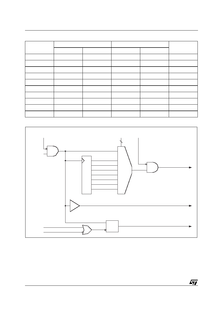
uPSD34xx - MCU CLOCK GENERATION
48/264
Table 21. PLLM and PLLD Values for Different f
OSC
Frequencies
Figure 14. Clock Generation Logic
f
OSC
(MHz)
PLLM[4:0]
PLLD[3:0]
f
USB_CLK
(MHz)
decimal
binary
decimal
binary
40.0
22
10110
8
1000
48.0
36.0
6
00110
1
0001
48.0
33.0
30
11110
9
1001
48.0
30.0
14
01110
3
0011
48.0
24.0
18
10010
3
0011
48.0
16.0
28
11100
3
0011
48.0
12.0
30
11110
2
0010
48.0
8.0
22
10110
0
0000
48.0
6.0
30
11110
0
0000
48.0
3.0
30
11110
≠1
1111
48.0
XTAL1 /2
XTAL1 /4
XTAL1 /2048
Q
Q
Q
M
U
X
XTAL1 (default)
XTAL1 /8
XTAL1 /16
Q
Q
XTAL1 /32
XTAL1 /1024
Q
Q
0
1
2
3
4
5
6
7
CLK
PLL
EN
XTAL1
(fOSC)
PCON[1]
CCON0[6]
PCON[1]: PD,
Power-Down Mode
PCON[2:0]: CPUPS[2:0],
Clock Pre-Scaler Select
PCON[0]: IDL,
Idle Mode
Clock Divider
MCU_CLK (fMCU)
(to: 8032, WDT)
PERIPH_CLK (fOSC)
(to: TIMER0/1/2, UART0/1, PCA0/1, SPI, I2C, ADC)
USB_CLK
3
AI10433
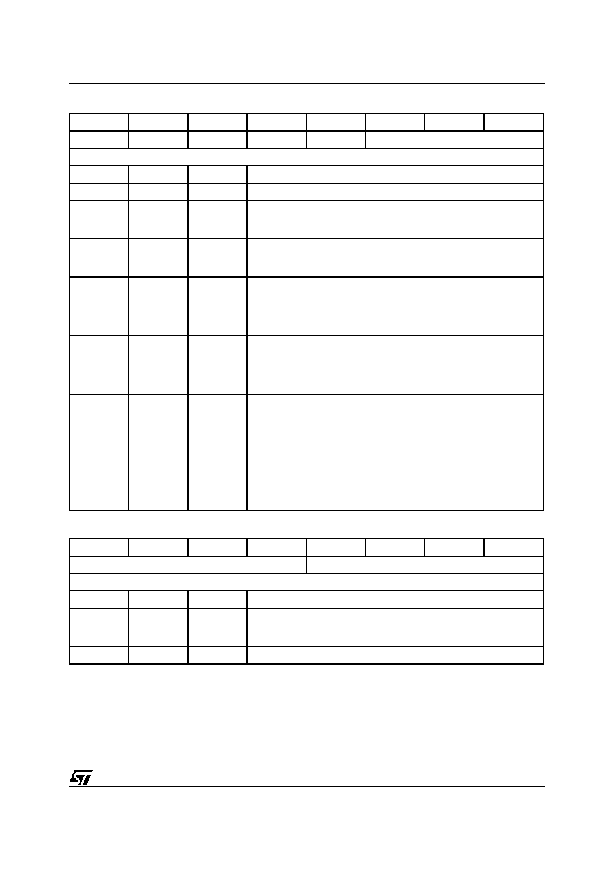
49/264
uPSD34xx - MCU CLOCK GENERATION
Table 22. CCON0: Clock Control Register (SFR F9h, reset value 50h)
Table 23. CCON1 PLL Control Register (SFR FAh, reset value 00h)
Bit 7
Bit 6
Bit 5
Bit 4
Bit 3
Bit 2
Bit 1
Bit 0
PLLM[4]
PLLEN
UPLLCE
DBGCE
CPUAR
CPUPS[2:0]
Details
Bit
Symbol
R/W
Definition
7
PLLM[4]
R,W
Upper bit of the 5-bit PLLM[4:0] Multiplier (Default: '0' for PLLM = 00h)
6
PLLEN
R,W
PLL Enable
0 = Disable PLL operation
1 = Enable PLL operation (Default condition after reset)
5
UPLLCE
R,W
USB Clock Enable
0 = USB clock is disabled (Default condition after reset)
1 = USB clock is enabled
4
DBGCE
R,W
Debug Unit Breakpoint Comparator Enable
0 = JTAG Debug Unit comparators are disabled
1 = JTAG Debug Unit comparators are enabled (Default condition after
reset)
3
CPUAR
R,W
Automatic MCU Clock Recovery
0 = There is no change of CPUPS[2:0] when an interrupt occurs.
1 = Contents of CPUPS[2:0] automatically become 000b whenever any
interrupt occurs.
2:0
CPUPS
R,W
MCUCLK Pre-Scaler
000b: f
MCU
= f
OSC
(Default after reset)
001b: f
MCU
= f
OSC
/2
010b: f
MCU
= f
OSC
/4
011b: f
MCU
= f
OSC
/8
100b: f
MCU
= f
OSC
/16
101b: f
MCU
= f
OSC
/32
110b: f
MCU
= f
OSC
/1024
111b: f
MCU
= f
OSC
/2048
Bit 7
Bit 6
Bit 5
Bit 4
Bit 3
Bit 2
Bit 1
Bit 0
PLLM[3:0]
PLLD[3:0]
Details
Bit
Symbol
R/W
Definition
7:4
PLLM[3:0]
R,W
Lower 4 bits of the 5-bit PLLM[4:0] Multiplier (Default after reset:
PLLM = 00h)
PLLM[4] is in the CCON0 Register.
3:0
PLLD[3:0]
R,W
4-bit PLL Divider (Default after reset: PLLD = 0h)

uPSD34xx - POWER SAVING MODES
50/264
POWER SAVING MODES
The uPSD34xx is a combination of two die, or
modules, each module having its own current con-
sumption characteristics. This section describes
reduced power modes for the MCU Module. See
the section,
Power Management, page 168
for re-
duced power modes of the PSD Module. Total cur-
rent consumption for the combined modules is
determined in the DC specifications at the end of
this document.
The MCU Module has three software-selectable
modes of reduced power operation.
Idle Mode
Power-down Mode
Reduced Frequency Mode
Idle Mode
Idle Mode will halt the 8032 MCU core while leav-
ing the MCU peripherals active (Idle Mode blocks
MCU_CLK only). For lowest current consumption
in this mode, it is recommended to disable all un-
used peripherals, before entering Idle mode (such
as the ADC and the Debug Unit breakpoint com-
parators). The following functions remain fully ac-
tive during Idle Mode (except if disabled by SFR
settings).
External Interrupts INT0 and INT1
Timer 0, Timer 1 and Timer 2
Supervisor reset from: LVD, JTAG Debug,
External RESET_IN_, but not the WTD
ADC
I
2
C Interface
UART0 and UART1 Interfaces
SPI Interface
Programmable Counter Array
USB Interface
An interrupt generated by any of these peripher-
als, or a reset generated from the supervisor, will
cause Idle Mode to exit and the 8032 MCU will re-
sume normal operation.
The output state on I/O pins of MCU ports 1, 3, and
4 remain unchanged during Idle Mode.
To enter Idle Mode, the 8032 MCU executes an in-
struction to set the IDL bit in the SFR named
PCON, shown in
Table 26., page 52
. This is the
last instruction executed in normal operating mode
before Idle Mode is activated. Once in Idle Mode,
the MCU status is entirely preserved, and there
are no changes to: SP, PSW, PC, ACC, SFRs,
DATA, IDATA, or XDATA.
The following are factors related to Idle Mode exit:
≠
Activation of any enabled interrupt will cause
the IDL bit to be cleared by hardware,
terminating Idle Mode. The interrupt is
serviced, and following the Return from
Interrupt instruction (RETI), the next
instruction to be executed will be the one
which follows the instruction that set the IDL
bit in the PCON SFR.
≠
After a reset from the supervisor, the IDL bit is
cleared, Idle Mode is terminated, and the MCU
restarts after three MCU machine cycles.
Power-down Mode
Power-down Mode will halt the 8032 core and all
MCU peripherals (Power-down Mode blocks
MCU_CLK, USB_CLK, and PERIPH_CLK). This
is the lowest power state for the MCU Module.
When the PSD Module is also placed in Power-
down mode, the lowest total current consumption
for the combined die is achieved for the
uPSD34xx. See
Power Management, page 168
in
the PSD Module section for details on how to also
place the PSD Module in Power-down mode. The
sequence of 8032 instructions is important when
placing both modules into Power-down Mode.
The instruction that sets the PD Bit in the SFR
named PCON (
Table 26., page 52
) is the last in-
struction executed prior to the MCU Module going
into Power-down Mode. Once in Power-down
Mode, the on-chip oscillator circuitry and all clocks
are stopped. The SFRs, DATA, IDATA,
and XDATA are preserved.
Power-down Mode is terminated only by a reset
from the supervisor, originating from the
RESET_IN_ pin, the Low-Voltage Detect circuit
(LVD), or a JTAG Debug reset command. Since
the clock to the WTD is not active during Power-
down mode, it is not possible for the supervisor to
generate a WDT reset.
Table 24., page 51
summarizes the status of I/O
pins and peripherals during Idle and Power-down
Modes on the MCU Module.
Table 25., page 51
shows the state of 8032 MCU address, data, and
control signals during these modes.
Reduced Frequency Mode
The 8032 MCU consumes less current when oper-
ating at a lower clock frequency. The MCU can re-
duce its own clock frequency at run-time by writing
to three bits, CPUPS[2:0], in the SFR named
CCON0 described in
Table 22., page 49
. These
bits effectively divide the clock frequency (f
OSC
)
coming in from the external crystal or oscillator de-
vice. The clock division range is from 1/2 to 1/
2048, and the resulting frequency is f
MCU
.
This MCU clock division does not affect any of the
peripherals, except for the WTD. The clock driving
the WTD is the same clock driving the 8032 MCU
core as shown in
Figure 14., page 48
.
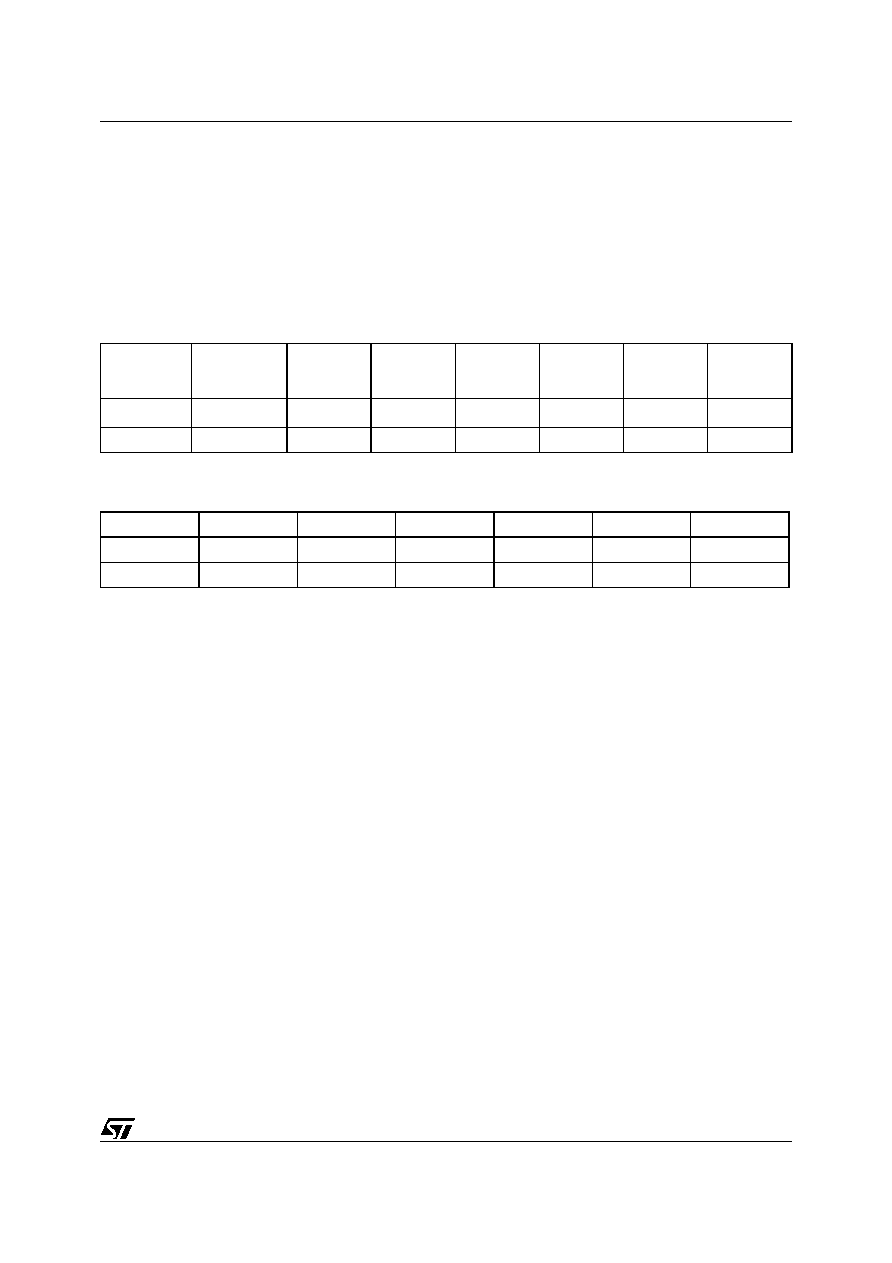
51/264
uPSD34xx - POWER SAVING MODES
MCU firmware may reduce the MCU clock fre-
quency at run-time to consume less current when
performing tasks that are not time critical, and then
restore full clock frequency as required to perform
urgent tasks.
Returning to full clock frequency is done automat-
ically upon an MCU interrupt, if the CPUAR Bit in
the SFR named CCON0 is set (the interrupt will
force CPUPS[2:0] = 000). This is an excellent way
to conserve power using a low frequency clock un-
til an event occurs that requires full performance.
See
Table 22., page 49
for details on CPUAR.
See the DC Specifications at the end of this docu-
ment to estimate current consumption based on
the MCU clock frequency.
Note: Some of the bits in the PCON SFR shown in
Table 26., page 52
are not related to power con-
trol.
Table 24. MCU Module Port and Peripheral Status during Reduced Power Modes
Note: 1. The Watchdog Timer is not active during Idle Mode. Other supervisor functions are active: LVD, external reset, JTAG Debug reset.
Table 25. State of 8032 MCU Bus Signals during Power-down and Idle Modes
Mode
Ports 1, 3, 4
SPI, I
2
C,
UART0,1
PCA,
TIMER
0,1,2
USB
ADC
EXT INT0,1
SUPER-
VISORY
Idle
Maintain Data
Active
Active
Active
Active
Active
Active
(1)
Power-down
Maintain Data
Disabled
Disabled
Disabled
Disabled
Disabled
Disabled
Mode
ALE
PSEN_
RD_
WR_
AD0-7
A8-15
Idle
0
1
1
1
FFh
FFh
Power-down
0
1
1
1
FFh
FFh

uPSD34xx - POWER SAVING MODES
52/264
Table 26. PCON: Power Control Register (SFR 87h, reset value 00h)
Bit 7
Bit 6
Bit 5
Bit 4
Bit 3
Bit 2
Bit 1
Bit 0
SMOD0
SMOD1
≠
POR
RCLK1
TCLK1
PD
IDL
Details
Bit
Symbol
R/W
Function
7
SMOD0
R,W
Baud Rate Double Bit (UART0)
0 = No Doubling
1 = Doubling
(See
UART Baud Rates, page 86
for details.)
6
SMOD1
R,W
Baud Rate Double Bit for 2nd UART (UART1)
0 = No Doubling
1 = Doubling
(See
UART Baud Rates, page 86
for details.)
5
≠
≠
Reserved
4
POR
R,W
Only a power-on reset sets this bit (cold reset). Warm reset will not set
this bit.
'0,' Cleared to zero with firmware
'1,' Is set only by a power-on reset generated by Supervisory circuit (see
Power-up Reset, page 68
for details).
3
RCLK1
R,W
Received Clock Flag (UART1)
(See
Table 43., page 77
for flag description.)
2
TCLK1
R,W
Transmit Clock Flag (UART1)
(See
Table 43., page 77
for flag description)
1
PD
R,W
Activate Power-down Mode
0 = Not in Power-down Mode
1 = Enter Power-down Mode
0
IDL
R,W
Activate Idle Mode
0 = Not in Idle Mode
1 = Enter Idle Mode

53/264
uPSD34xx - OSCILLATOR AND EXTERNAL COMPONENTS
OSCILLATOR AND EXTERNAL COMPONENTS
The oscillator circuit of uPSD34xx devices is a sin-
gle stage, inverting amplifier in a Pierce oscillator
configuration. The internal circuitry between pins
XTAL1 and XTAL2 is basically an inverter biased
to the transfer point. Either an external quartz crys-
tal or ceramic resonator can be used as the feed-
back element to complete the oscillator circuit.
Both are operated in parallel resonance. Ceramic
resonators are lower cost, but typically have a wid-
er frequency tolerance than quartz crystals. Alter-
natively, an external clock source from an
oscillator or other active device may drive the
uPSD34xx oscillator circuit input directly, instead
of using a crystal or resonator.
The minimum frequency of the quartz crystal, ce-
ramic resonator, or external clock source is 3MHz
if the USB is used. The minimum is 8MHz if I
2
C is
used. The maximum is 40MHz in all cases. This
frequency is f
OSC
, which can be divided internally
as described in
MCU CLOCK
GENERATION, page 47
.
The pin XTAL1 is the high gain amplifier input, and
XTAL2 is the output. To drive the uPSD34xx de-
vice externally from an oscillator or other active
device, XTAL1 is driven and XTAL2 is left open-
circuit. This external source should drive a logic
low at the voltage level of 0.3 V
CC
or below, and
logic high at 0.7V V
CC
or above, up to 5.5V V
CC
.
The XTAL1 input is 5V tolerant.
Most of the quartz crystals in the range of 25MHz
to 40MHz operate in the third overtone frequency
mode. An external LC tank circuit at the XTAL2
output of the oscillator circuit is needed to achieve
the third overtone frequency, as shown in
Figure
15., page 53
. Without this LC circuit, the crystal
will oscillate at a fundamental frequency mode that
is about 1/3 of the desired overtone frequency.
Note: In
Figure 15., page 53
crystals which are
specified to operate in fundamental mode (not
overtone mode) do not need the LC circuit compo-
nents. Since quartz crystals and ceramic resona-
tors have their own characteristics based on their
manufacturer, it is wise to also consult the manu-
facturer's recommended values for external com-
ponents.
Figure 15. Oscillator and Clock Connections
Crystal or Resonator
Usage
Direct Drive
XTAL1
(in)
XTAL1
(in)
XTAL2
(out)
XTAL2
(out)
C1
C2
XTAL
(fOSC)
L1
C3
No Connect
External Ocsillator or
Active Clock Source
XTAL (fOSC)
C1 = C2
C3
L1
Ceramic Resonator
40 - 50pF
None
Crystal, fundamental mode (3-40MHz)
15-33pF
None
None
None
Crystal, overtone mode (25-40MHz)
20pF
10nF
2.2µH
AI09198

uPSD34xx - I/O PORTS of MCU MODULE
54/264
I/O PORTS OF MCU MODULE
The MCU Module has three 8-bit I/O ports: Port 1,
Port 3, and Port 4. The PSD Module has four other
I/O ports: Port A, B, C, and D. This section de-
scribes only the I/O ports on the MCU Module.
I/O ports will function as bi-directional General
Purpose I/O (GPIO), but the port pins can have al-
ternate functions assigned at run-time by writing to
specific SFRs. The default operating mode (during
and after reset) for all three ports is GPIO input
mode. Port pins that have no external connection
will not float because each pin has an internal
weak pull-up (~150K ohms) to V
CC
.
I/O ports 3 and 4 are 5V tolerant, meaning they
can be driven/pulled externally up to 5.5V without
damage. The pins on Port 4 have a higher current
capability than the pins on Ports 1 and 3.
Three additional MCU ports (only on 80-pin
uPSD34xx devices) are dedicated to bring out the
8032 MCU address, data, and control signals to
external pins. One port, named MCUAD[7:0], has
eight multiplexed address/data bidirectional sig-
nals. The third port has MCU bus control outputs:
read, write, program fetch, and address latch.
These ports are typically used to connect external
parallel peripherals and memory devices, but they
may NOT be used as GPIO. Notice that the eight
upper address signals do not come out to pins on
the port. If high-order address signals are required
on external pins (MCU addresses A[15:8]), then
these address signals can be brought out as need-
ed to PLD output pins or to the Address Out mode
pins on PSD Module ports. See PSD Module sec-
tion, "
Latched Address Output Mode, page 208
for
details.
Figure 16., page 56
represents the flexibility of pin
function routing controlled by the SFRs. Each of
the 24 pins on three ports, P1, P3, and P4, may be
individually routed on a pin-by-pin basis to a de-
sired function.
MCU Port Operating Modes
MCU port pins can operate as GPIO or as alter-
nate functions (see
Figure 17., page 57
through
Figure 19., page 58
).
Depending on the selected pin function, a particu-
lar pin operating mode will automatically be used:
GPIO - Quasi-bidirectional mode
UART0, UART1 - Quasi-bidirectional mode
SPI - Quasi-bidirectional mode
I2C - Open drain mode
ADC - Analog input mode
PCA output - Push-Pull mode
PCA input - Input only (Quasi-bidirectional)
Timer 0,1,2 - Input only (Quasi-bidirectional)
GPIO Function. Ports in GPIO mode operate as
quasi-bidirectional pins, consistent with standard
8051 architecture. GPIO pins are individually con-
trolled by three SFRs:
SFR, P1 (
Table 27., page 58
)
SFR, P3 (
Table 28., page 59
)
SFR, P4 (
Table 29., page 59
)
These SFRs can be accessed using the Bit Ad-
dressing mode, an efficient way to control individ-
ual port pins.
GPIO Output. Simply stated, when a logic '0' is
written to a bit in any of these port SFRs while in
GPIO mode, the corresponding port pin will enable
a low-side driver, which pulls the pin to ground,
and at the same time releases the high-side driver
and pull-ups, resulting in a logic '0' output. When a
logic '1' is written to the SFR, the low-side driver is
released, the high-side driver is enabled for just
one MCU_CLK period to rapidly make the 0-to1
transition on the pin, while weak active pull-ups
(total ~150K
) to V
CC
are enabled. This structure
is consistent with standard 8051 architecture. The
high side driver is momentarily enabled only for 0-
to-1 transitions, which is implemented with the de-
lay function at the latch output as pictured in
Fig-
ure 17., page 57
,
Figure 18., page 57
, and
Figure
19., page 58
. After the high-side driver is disabled,
the two weak pull-ups remain enabled resulting in
a logic '1' output at the pin, sourcing I
OH
uA to an
external device. Optionally, an external pull-up re-
sistor can be added if additional source current is
needed while outputting a logic '1.'

55/264
uPSD34xx - I/O PORTS of MCU MODULE
GPIO Input. To use a GPIO port pin as an input,
the low-side driver to ground must be disabled, or
else the true logic level being driven on the pin by
an external device will be masked (always reads
logic '0'). So to make a port pin "input ready", the
corresponding bit in the SFR must have been set
to a logic '1' prior to reading that SFR bit as an in-
put. A reset condition forces SFRs P1, P3, and P4
to FFh, thus all three ports are input ready after re-
set.
When a pin is used as an input, the stronger pull-
up "A" maintains a solid logic '1' until an external
device drives the input pin low. At this time, pull-up
"A" is automatically disabled, and only pull-up "B"
will source the external device I
IH
uA, consistent
with standard 8051 architecture.
GPIO Bi-Directional. It is possible to operate indi-
vidual port pins in bi-directional mode. For an out-
put, firmware would simply write the
corresponding SFR bit to logic '1' or '0' as needed.
But before using the pin as an input, firmware must
first ensure that a logic '1' was the last value writ-
ten to the corresponding SFR bit prior to reading
that SFR bit as an input.
GPIO Current Capability. A GPIO pin on Port 4
can sink twice as much current than a pin on either
Port 1 or Port 3 when the low-side driver is output-
ting a logic '0' (I
OL
). See the DC specifications at
the end of this document for full details.
Reading Port Pin vs. Reading Port Latch. When
firmware reads the GPIO ports, sometimes the ac-
tual port pin is sampled in hardware, and some-
times the port SFR latch is read and not the actual
pin, depending on the type of MCU instruction
used. These two data paths are shown in
Figure
17., page 57
through
Figure 19., page 58
. SFR
latches are read (and not the pins) only when the
read is part of a read-modify-write instruction and
the write destination is a bit or bits in a port SFR.
These instructions are: ANL, ORL, XRL, JBC,
CPL, INC, DEC, DJNZ, MOV, CLR, and SETB. All
other types of reads to port SFRs will read the ac-
tual pin logic level and not the port latch. This is
consistent with 8051 architecture.
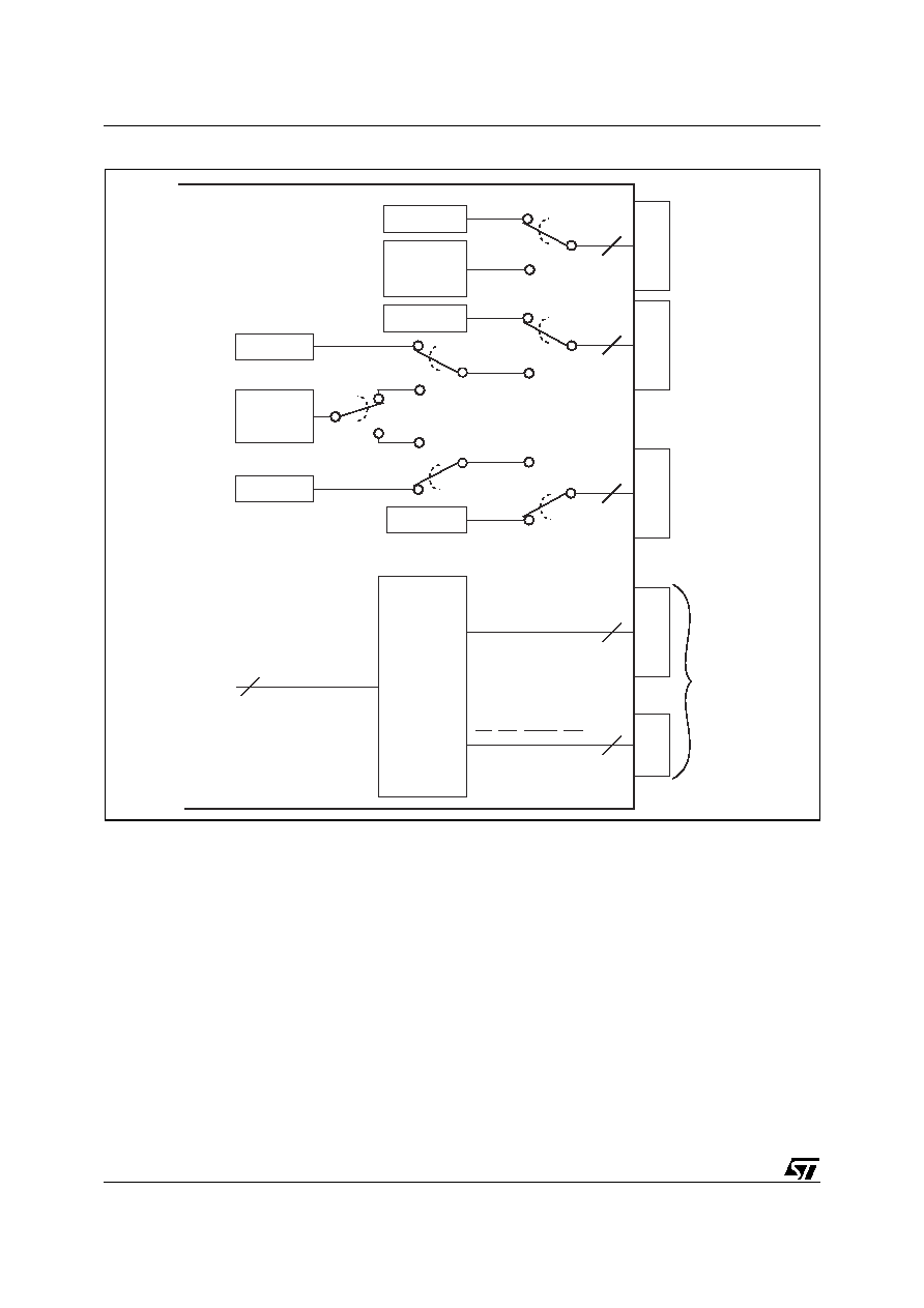
uPSD34xx - I/O PORTS of MCU MODULE
56/264
Figure 16. MCU Module Port Pin Function Routing
8
P3
P1
P4
M
C
U
A
D
GPIO (8)
UART0 (2)
TIMER0/1 (4)
I
2
C (2)
GPIO (8)
GPIO (8)
TIMER2 (2)
UART1 (2)
SPI (4)
ADC (8)
PCA (8)
8032 MCU
CORE
Low Addr & Data[7:0]
8
Hi Address [15:8]
(Available on PSD
Module Pins)
MCU Module
8
On 80-pin
Devices
Only
Ports
C
N
T
L
RD, WR, PSEN, ALE
4
SFR
8
8
SFR
SFR
SFR
SFR
SFR
AI09199b

57/264
uPSD34xx - I/O PORTS of MCU MODULE
Figure 17. MCU I/O Cell Block Diagram for Port 1
Figure 18. MCU I/O Cell Block Diagram for Port 3
P1.X Pin
Analog_Alt_Func_En
Analog_Pin_In
Q
D
PRE
SFR
P1.X
Latch
8032 Data Bus Bit
GPIO P1.X SFR
Write Latch
MCU_Reset
P1.X SFR Read Latch
(for R-M-W instructions)
P1.X SFR Read Pin
Select_Alternate_Func
Digital_Pin_Data_In
IN 1
IN 0
Y
MUX
VCC
VCC
VCC
SEL
WEAK
PULL-UP, B
STONGER
PULL-UP, A
LOW
SIDE
HIGH
SIDE
DELAY,
1 MCU_CLK
DELAY,
1 MCU_CLK
Q
Digital_Alt_Func_Data_Out
AI09600
P3.X Pin
Digital_Pin_Data_In
Q
D
PRE
SFR
P3.X
Latch
8032 Data Bus Bit
GPIO P3.X SFR
Write Latch
MCU_Reset
P3.X SFR Read Latch
(for R-M-W instructions)
P3.X SFR Read Pin
Select_Alternate_Func
Disables High-Side Driver
IN 1
IN 0
Y
MUX
VCC
VCC
VCC
SEL
Enable_I
2
C
WEAK
PULL-UP, B
STONGER
PULL-UP, A
LOW
SIDE
HIGH
SIDE
DELAY,
1 MCU_CLK
DELAY,
1 MCU_CLK
Q
Digital_Alt_Func_Data_Out
AI09601
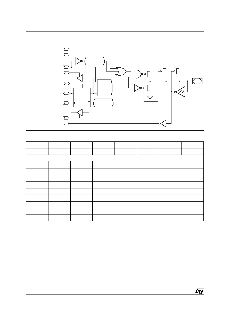
uPSD34xx - I/O PORTS of MCU MODULE
58/264
Figure 19. MCU I/O Cell Block Diagram for Port 4
Table 27. P1: I/O Port 1 Register (SFR 90h, reset value FFh)
Note: 1. Write '1' or '0' for pin output. Read for pin input, but prior to READ, this bit must have been set to '1' by firmware or by a reset event.
Bit 7
Bit 6
Bit 5
Bit 4
Bit 3
Bit 2
Bit 1
Bit 0
P1.7
P1.6
P1.5
P1.4
P1.3
P1.2
P1.1
P1.0
Details
Bit
Symbol
R/W
Function
(1)
7
P1.7
R,W
Port pin 1.7
6
P1.6
R,W
Port pin 1.6
5
P1.5
R,W
Port pin 1.5
4
P1.4
R,W
Port pin 1.4
3
P1.3
R,W
Port pin 1.3
2
P1.2
R,W
Port pin 1.2
1
P1.1
R,W
Port pin 1.1
0
P1.0
R,W
Port pin 1.0
P4.X Pin
Digital_Pin_Data_In
Q
D
PRE
SFR
P4.X
Latch
8032 Data Bus Bit
GPIO P4.X SFR
Write Latch
MCU_Reset
P4.X SFR Read Latch
(for R-M-W instructions)
P4.X SFR Read Pin
Select_Alternate_Func
For PCA Alternate Function
IN 1
IN 0
Y
MUX
VCC
VCC
VCC
SEL
Enable_Push_Pull
WEAK
PULL-UP, B
STONGER
PULL-UP, A
LOW
SIDE
HIGH
SIDE
DELAY,
1 MCU_CLK
DELAY,
1 MCU_CLK
Q
Digital_Alt_Func_Data_Out
AI09602

59/264
uPSD34xx - I/O PORTS of MCU MODULE
Table 28. P3: I/O Port 3 Register (SFR B0h, reset value FFh)
Note: 1. Write '1' or '0' for pin output. Read for pin input, but prior to READ, this bit must have been set to '1' by firmware or by a reset event.
Table 29. P4: I/O Port 4 Register (SFR C0h, reset value FFh)
Note: 1. Write '1' or '0' for pin output. Read for pin input, but prior to READ, this bit must have been set to '1' by firmware or by a reset event.
Bit 7
Bit 6
Bit 5
Bit 4
Bit 3
Bit 2
Bit 1
Bit 0
P3.7
P3.6
P3.5
P3.4
P3.3
P3.2
P3.1
P3.0
Details
Bit
Symbol
R/W
Function
(1)
7
P3.7
R,W
Port pin 3.7
6
P3.6
R,W
Port pin 3.6
5
P3.5
R,W
Port pin 3.5
4
P3.4
R,W
Port pin 3.4
3
P3.3
R,W
Port pin 3.3
2
P3.2
R,W
Port pin 3.2
1
P3.1
R,W
Port pin 3.1
0
P3.0
R,W
Port pin 3.0
Bit 7
Bit 6
Bit 5
Bit 4
Bit 3
Bit 2
Bit 1
Bit 0
P4.7
P4.6
P4.5
P4.4
P4.3
P4.2
P4.1
P4.0
Details
Bit
Symbol
R/W
Function
(1)
7
P4.7
R,W
Port pin 4.7
6
P4.6
R,W
Port pin 4.6
5
P4.5
R,W
Port pin 4.5
4
P4.4
R,W
Port pin 4.4
3
P4.3
R,W
Port pin 4.3
2
P4.2
R,W
Port pin 4.2
1
P4.1
R,W
Port pin 4.1
0
P4.0
R,W
Port pin 4.0

uPSD34xx - I/O PORTS of MCU MODULE
60/264
Alternate Functions. There are five SFRs used
to control the mapping of alternate functions onto
MCU port pins, and these SFRs are depicted as
switches in
Figure 16., page 56
.
Port 3 uses the SFR, P3SFS (
Table
30., page 61
).
Port 1 uses SFRs, P1SFS0 (
Table
31., page 61
) and P1SFS1 (
Table
32., page 61
).
Port 4 uses SFRs, P4SFS0 (
Table
34., page 62
) and P4SFS1 (
Table
35., page 62
).
Since these SFRs are cleared by a reset, then by
default all port pins function as GPIO (not the alter-
nate function) until firmware initializes these SFRs.
Each pin on each of the three ports can be inde-
pendently assigned a different function on a pin-
by-pin basis.
The peripheral functions Timer 2, UART1, and I
2
C
may be split independently between Port 1 and
Port 4 for additional flexibility by giving a wider
choice of peripheral usage on a limited number of
device pins.
When the selected alternate function is UART0,
UART1, or SPI, then the related pins are in quasi-
bidirectional mode, including the use of the high-
side driver for rapid 0-to-1 output transitions. The
high-side driver is enabled for just one MCU_CLK
period on 0-to-1 transitions by the delay function at
the "digital_alt_func_data_out" signal pictured in
Figure 17., page 57
through
Figure 19., page 58
.
If the alternate function is Timer 0, Timer 1, Timer
2, or PCA input, then the related pins are in quasi-
bidirectional mode, but input only.
If the alternate function is ADC, then for each pin
the pull-ups, the high-side driver, and the low-side
driver are disabled. The analog input is routed di-
rectly to the ADC unit. Only Port 1 supports analog
functions (
Figure 17., page 57
). Port 1 is not 5V
tolerant.
If the alternate function is I
2
C, the related pins will
be in open drain mode, which is just like quasi-bi-
directional mode but the high-side driver is not en-
abled for one cycle when outputting a 0-to-1
transition. Only the low-side driver and the internal
weak pull-ups are used. Only Port 3 supports
open-drain mode (
Figure 18., page 57
). I
2
C re-
quires the use of an external pull-up resistor on
each bus signal, typically 4.7K
to V
CC
.
If the alternate function is PCA output, then the re-
lated pins are in push-pull mode, meaning the pins
are actively driven and held to logic '1' by the high-
side driver, or actively driven and held to logic '0'
by the low-side driver. Only Port 4 supports push-
pull mode (
Figure 19., page 58
). Port 4 push-pull
pins can source I
OH
current when driving logic '1,'
and sink I
OL
current when driving logic '0.' This
current is significantly more than the capability of
pins on Port 1 or Port 3 (see
Table
156., page 238
).
For example, to assign these port functions:
Port 1: UART1, ADC[1:0], P1[7:4] are GPIO
Port 3: UART0, I
2
C, P3[5:2] are GPIO
Port 4: TCM0, SPI, P4[3:1] are GPIO
The following values need to be written to the
SFRs:
P1SFS0 = 00001111b, or 0Fh
P1SFS1 = 00000011b , or 03h
P3SFS = 11000011b, or C3h
P4SFS0 = 11110001b, or F1h
P4SFS1 = 11110000b, or F0h

61/264
uPSD34xx - I/O PORTS of MCU MODULE
Table 30. P3SFS: Port 3 Special Function Select Register (SFR 91h, reset value 00h)
Table 31. P1SFS0: Port 1 Special Function Select 0 Register (SFR 8Eh, reset value 00h)
Table 32. P1SFS1: Port 1 Special Function Select 1 Register (SFR 8Fh, reset value 00h)
Table 33. P1SFS0 and P1SFS1 Details
Bit 7
Bit 6
Bit 5
Bit 4
Bit 3
Bit 2
Bit 1
Bit 0
P3SFS7
P3SFS6
P3SFS5
P3SFS4
P3SFS3
P3SFS2
P3SFS1
P3SFS0
Details
Port 3 Pin
R/W
Default Port Function
Alternate Port Function
P3SFS[i] - 0; Port 3 Pin, i = 0..7
P3SFS[i] - 1; Port 3 Pin, i = 0..7
0
R,W
GPIO
UART0 Receive, RXD0
1
R,W
GPIO
UART0 Transmit, TXD0
2
R,W
GPIO
Ext Intr 0/Timer 0 Gate, EXT0INT/TG0
3
R,W
GPIO
Ext Intr 1/Timer 1 Gate, EXT1INT/TG1
4
R,W
GPIO
Counter 0 Input, C0
5
R,W
GPIO
Counter 0 Input, C1
6
R,W
GPIO
I
2
C Data, I2CSDA
7
R,W
GPIO
I
2
C Clock, I2CCL
Bit 7
Bit 6
Bit 5
Bit 4
Bit 3
Bit 2
Bit 1
Bit 0
P1SF07
P1SF06
P1SF05
P1SF04
P1SF03
P1SF02
P1SF01
P1SF00
Details
Bit 7
Bit 6
Bit 5
Bit 4
Bit 3
Bit 2
Bit 1
Bit 0
P1SF17
P1SF16
P1SF15
P1SF14
P1SF13
P1SF12
P1SF11
P1SF10
Port 1 Pin
R/W
Default Port Function
Alternate 1 Port Function
Alternate 2 Port Function
P1SFS0[i] = 0
P1SFS1[i] = x
P1SFS0[i] = 1
P1SFS1[i] = 0
P1SFS0[i] = 1
P1SFS1[i] = 1
Port 1 Pin, i = 0.. 7
Port 1 Pin, i = 0.. 7
Port 1 Pin, i = 0.. 7
0
R,W
GPIO
Timer 2 Count Input, T2
ADC Chn 0 Input, ADC0
1
R,W
GPIO
Timer 2 Trigger Input, TX2
ADC Chn 1 Input, ADC1
2
R,W
GPIO
UART1 Receive, RXD1
ADC Chn 2 Input, ADC2
3
R,W
GPIO
UART1 Transmit, TXD1
ADC Chn 3 Input, ADC3
4
R,W
GPIO
SPI Clock, SPICLK
ADC Chn 4 Input, ADC4
5
R,W
GPIO
SPI Receive, SPIRXD
ADC Chn 5 Input, ADC5
6
R,W
GPIO
SPI Transmit, SPITXD
ADC Chn 6 Input, ADC6
7
R,W
GPIO
SPI Select, SPISEL_
ADC Chn 7 Input, ADC7
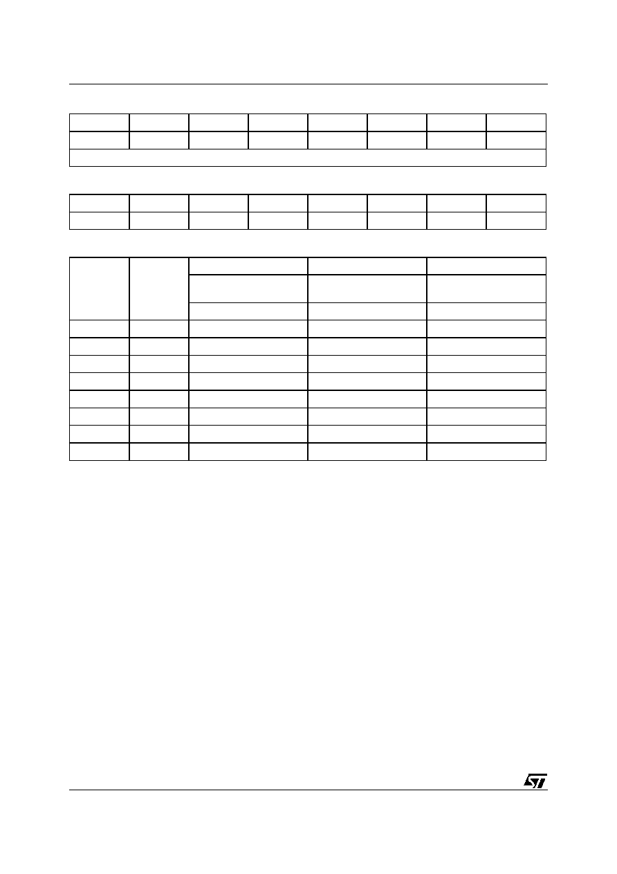
uPSD34xx - I/O PORTS of MCU MODULE
62/264
Table 34. P4SFS0: Port 4 Special Function Select 0 Register (SFR 92h, reset value 00h)
Table 35. P4SFS1: Port 4 Special Function Select 1 Register (SFR 93h, reset value 00h)
Table 36. P4SFS0 and P4SFS1 Details
Bit 7
Bit 6
Bit 5
Bit 4
Bit 3
Bit 2
Bit 1
Bit 0
P4SF07
P4SF06
P4SF05
P4SF04
P4SF03
P4SF02
P4SF01
P4SF00
Details
Bit 7
Bit 6
Bit 5
Bit 4
Bit 3
Bit 2
Bit 1
Bit 0
P4SF17
P4SF16
P4SF15
P4SF14
P4SF13
P4SF12
P4SF11
P4SF10
Port 4 Pin
R/W
Default Port Function
Alternate 1 Port Function
Alternate 2 Port Function
P4SFS0[i] = 0
P4SFS1[i] = x
P4SFS0[i] = 1
P4SFS1[i] = 0
P4SFS0[i] = 1
P4SFS1[i] = 1
Port 4 Pin, i = 0.. 7
Port 4 Pin, i = 0.. 7
Port 4 Pin, i = 0.. 7
0
R,W
GPIO
PCA0 Module 0, TCM0
Timer 2 Count Input, T2
1
R,W
GPIO
PCA0 Module 1, TCM1
Timer 2 Trigger Input, TX2
2
R,W
GPIO
PCA0 Module 2, TCM2
UART1 Receive, RXD1
3
R,W
GPIO
PCA0 Ext Clock, PCACLK0
UART1 Transmit, TXD1
4
R,W
GPIO
PCA1 Module 3, TCM3
SPI Clock, SPICLK
5
R,W
GPIO
PCA1 Module 4, TCM4
SPI Receive, SPIRXD
6
R,W
GPIO
PCA1 Module 5, TCM5
SPI Transmit, SPITXD
7
R,W
GPIO
PCA1 Ext Clock, PCACLK1
SPI Select, SPISEL_
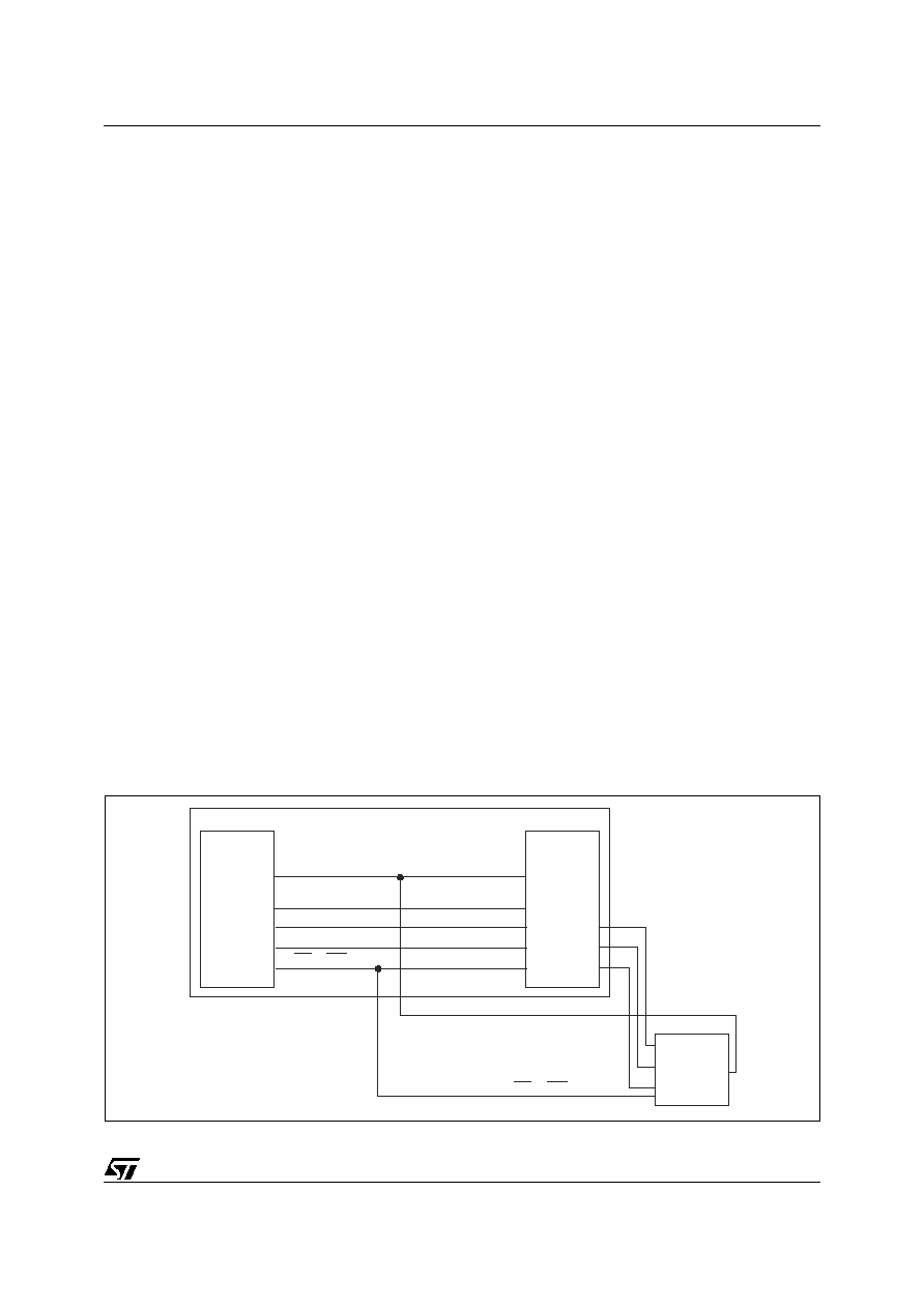
63/264
uPSD34xx - MCU BUS INTERFACE
MCU BUS INTERFACE
The MCU Module has a programmable bus inter-
face which is a modified 8032 bus with 16 multi-
plexed address and data lines. The bus supports
four types of data transfer (16- or 8-bit), each
transfer is to/from a memory location external to
the MCU Module:
≠
Code Fetch cycle using the PSEN signal: fetch
a 16-bit code word for filling the pre-fetch
queue. The CPU fetches a code byte from the
PFQ for execution;
≠
Code Read cycle using PSEN: read a 16-bit
code word using the MOVC (Move Constant)
instruction. The code word is routed directly to
the CPU and by-pass the PFQ;
≠
XDATA Read cycle using the RD signal: read
a data byte using the MOVX (Move eXternal)
instruction; and
≠
XDATA Write cycle using the WR signal: write
a data byte using the MOVX instruction
PSEN Bus Cycles
In a PSEN bus cycle, the MCU module fetches the
instruction from the 16-bit program memory in the
PSD module. The multiplexed address/data bus
AD[15:0] is connected to the PSD module for 16-
bit data transfer. The uPSD34xx does not support
external PSEN cycles and cannot fetch instruction
from other external program memory devices.
READ or WRITE Bus Cycles
In an XDATA READ or WRITE bus cycle, the
MCU's multiplexed AD[15:0] bus is connected to
the PSD module, but only the lower bytes AD[7:0]
are used for the 8-bit data transfer. The AD[7:0]
lines are also connected to pins in the 80-pin pack-
age for accessing external devices. If the high ad-
dress byte A[15:8] is needed for external devices,
Port B in the PSD Module can be configured to
provide the latched A[15:8] address outputs.
Connecting External Devices to the MCU Bus
The uPSD34xx supports 8-bit only external I/O or
Data memory devices. The READ and WRITE
data transfer is carried out on the AD[7:0] bus
which is available in the 80-pin package. The ad-
dress lines can be brought out to the external de-
vices in one of three ways:
1.
Configure Ports B and A of the PSD Module in
Address Output mode, as shown in Figure
20
;
2.
Use Port B together with an external latch, as
shown in
Figure 21., page 64
. The external
latch latches the low address byte from the
AD[7:0] bus with the ALE signal.This
configuration is for design where Port A is
needed for CPLD functions; and
3.
Configure the microcell in the CPLD to output
any address line to any of the CPLD output
pins. This is the most flexible implementation
but requires the use of CPLD resources.
Ports A and B in the PSD Module can be config-
ured in the PSDsoft to provide latched MCU ad-
dress A[7:0] and A[15:8] (see
PSD Module
Detailed Operation, page 178
for details on how to
enable Address Output mode). The latched ad-
dress outputs on the ports are pin configurable.
For example, Port B pins PB[2:0] can be enabled
to provide A[10:8] and the remaining pins can be
configured for other functions such as generating
chip selects to the external devices.
Figure 20. Connecting External Devices using Ports A and B for Address AD[15:0]
uPSD34xx
PSD
Module
External
8-bit
Device
MCU
Module
AI10434
AD[7:0]
D[7:0]
A8-15
A0-7
Port A
CS
Port B
AD[15:8]
PSEN
ALE
RD or WR
RD or WR

uPSD34xx - MCU BUS INTERFACE
64/264
Figure 21. Connecting External Devices using Port A and an External Latch for Address AD[15:0]
Programmable Bus Timing
The length of the bus cycles are user programma-
ble at run time. The number of MCU_CLK periods
in a bus cycle can be specified in the SFR register
named BUSCON (see
Table 37., page 65
). By de-
fault, the BUSCON Register is loaded with long
bus cycle times (6 MCU_CLK periods) after a re-
set condition. It is important that the post-reset ini-
tialization firmware sets the bus cycle times
appropriately to get the most performance, ac-
cording to
Table 38., page 66
. Keep in mind that
the PSD Module has a faster Turbo Mode (default)
and a slower but less power consuming Non-Tur-
bo Mode. The bus cycle times must be pro-
grammed in BUSCON to optimize for each mode
as shown in
Table 38.
See
PSD Module Detailed
Operation, page 178
for more details.
It is not possible to specify in the BUSCON Regis-
ter a different number of MCU_CLK periods for
various address ranges. For example, the user
cannot specify 4 MCU_CLK periods for RD read
cycles to one address range on the PSD Module,
and 5 MCU_CLK periods for RD read cycles to a
different address range on an external device.
However, the user can specify one number of
clock periods for PSEN read cycles and a different
number of clock periods for RD or WR cycles (see
Figure
Figure 22., page 65
).
Controlling the PFQ and BC
The BUSCON Register allows firmware to enable
and disable the PFQ and BC at run-time. Some-
times it may be desired to disable the PFQ and BC
to ensure deterministic execution. The dynamic
action of the PFQ and BC may cause varying pro-
gram execution times depending on the events
that happen prior to a particular section of code of
interest. For this reason, it is not recommended to
implement timing loops in firmware, but instead
use one of the many hardware timers in the
uPSD34xx. By default, the PFQ and BC are en-
abled after a reset condition.
Important: Disabling the PFQ or BC will seriously
reduce MCU performance.
uPSD34xx
PSD
Module
External
8-bit
Device
L
A
T
C
H
MCU
Module
AI10435
AD[7:0]
D[7:0]
A7-0
A8-15
CS
Port B
AD[15:8]
PSEN
ALE
RD or WR
RD or WR
65/264
uPSD34xx - MCU BUS INTERFACE
Figure 22. A RD or PSEN Bus Cycle Set to 5 MCU_CLK
Note: 1. The PSEN cycle is 16-bit, while the RD cycle is 8-bit only.
2. A PSEN bus cycle in progress may be aborted before completion if the PFQ and Branch Cache (BC) determines the current code
fetch cycle is not needed.
3. Whenever the same number of MCU_CLK periods is specified in BUSCON for both PSEN and RD cycles, the bus cycle timing is
typically identical for each of these types of bus cycles. In this case, the only time PSEN read cycles are longer than RD read cycles
is when the PFQ issues a stall while reloading. PFQ stalls do not affect RD read cycles. By comparison, in many traditional 8051
architectures, RD bus cycles are always longer than PSEN bus cycles.
Table 37. BUSCON: Bus Control Register (SFR 9Dh, reset value EBh)
Bit 7
Bit 6
Bit 5
Bit 4
Bit 3
Bit 2
Bit 1
Bit 0
EPFQ
EBC
WRW[1:0]
RDW[1:0]
CW[1:0]
Details
Bit
Symbol
R/W
Definition
7
EPFQ
R,W
Enable Pre-Fetch Queue
0 = PFQ is disabled
1 = PFQ is enabled (default)
6
EBC
R,W
Enable Branch Cache
0 = BC is disabled
1 = BC is enabled (default)
5:4
WRW[1:0]
R,W
WR Wait, number of MCU_CLK periods for WR write bus cycle during
any MOVX instruction
00b: 4 clock periods
01b: 5 clock periods
10b: 6 clock periods (default)
11b: 7 clock periods
3:2
RDW[1:0]
R,W
RD Wait, number of MCU_CLK periods for RD read bus cycle during any
MOVX instruction
00b: 4 clock periods
01b: 5 clock periods
10b: 6 clock periods (default)
11b: 7 clock periods
1:0
CW[1:0]
R,W
Code Wait, number of MCU_CLK periods for PSEN read bus cycle
during any code byte fetch or during any MOVC code byte read
instruction. Periods will increase with PFQ stall
00b: 3 clock periods - exception, for MOVC instructions this setting
results 4 clock periods
01b: 4 clock periods
10b: 5 clock periods
11b: 6 clock periods (default)
A0-A15
MCU Clock
ALE
AD0-AD15
1
2
3
4
5
D0-D15
(1)
5-Clock Bus Cycle
RD/PSEN
(2,3)
AI10436
uPSD34xx - MCU BUS INTERFACE
66/264
Table 38. Number of MCU_CLK Periods Required to Optimize Bus Transfer Rate
Note: 1. V
DD
of the PSD Module
2. "Turbo mode PSD" means that the PSD Module is in the faster, Turbo mode (default condition). A PSD Module in Non-Turbo mode
is slower, but consumes less current. See PSD Module section, titled "PLD Non-Turbo Mode" for details.
MCU Clock Frequency,
MCU_CLK (f
MCU
)
CW[1:0] Clk Periods
RDW[1:0] Clk
Periods
WRW[1:0] Clk
Periods
3.3V
(1)
5V
(1)
3.3V
(1)
5V
(1)
3.3V
(1)
5V
(1)
40MHz, Turbo mode PSD
(2)
5
4
5
4
5
4
40MHz, Non-Turbo mode PSD
6
5
6
5
6
5
36MHz, Turbo mode PSD
5
4
5
4
5
4
36MHz, Non-Turbo mode PSD
6
4
6
4
6
4
32MHz, Turbo mode PSD
5
4
5
4
5
4
32MHz, Non-Turbo mode PSD
5
4
5
4
5
4
28MHz, Turbo mode PSD
4
3
4
4
4
4
28MHz, Non-Turbo mode PSD
5
4
5
4
5
4
24MHz, Turbo mode PSD
4
3
4
4
4
4
24MHz, Non-Turbo mode PSD
4
3
4
4
4
4
20MHz and below, Turbo mode PSD
3
3
4
4
4
4
20MHz and below, Non-Turbo mode PSD
3
3
4
4
4
4
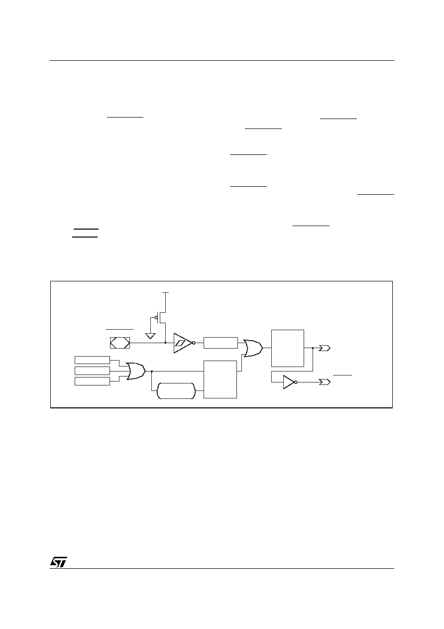
67/264
uPSD34xx - SUPERVISORY FUNCTIONS
SUPERVISORY FUNCTIONS
Supervisory circuitry on the MCU Module will issue
an internal reset signal to the MCU Module and si-
multaneously to the PSD Module as a result of any
of the following four events:
≠
The external RESET_IN pin is asserted
≠
The Low Voltage Detect (LVD) circuitry has
detected a voltage on V
CC
below a specific
threshold (power-on or voltage sags)
≠
The JTAG Debug interface has issued a reset
command
≠
The Watch Dog Timer (WDT) has timed out
The resulting internal reset signal, MCU_RESET,
will force the 8032 into a known reset state while
asserted, and then 8032 program execution will
jump to the reset vector at program address 0000h
just after MCU_RESET is deasserted. The MCU
Module will also assert an active low internal reset
signal, RESET, to the PSD Module. If needed, the
signal RESET can be driven out to external sys-
tem components through any PLD output pin on
the PSD Module. When driving this
"RESET_OUT" signal from a PLD output, the user
can choose to make it either active-high or active-
low logic, depending on the PLD equation.
External Reset Input Pin, RESET_IN
The RESET_IN pin can be connected directly to a
mechanical reset switch or other device which
pulls the signal to ground to invoke a reset.
RESET_IN is pulled up internally and enters a
Schmitt trigger input buffer with a voltage hystere-
sis of V
RST_HYS
for immunity to the effects of slow
signal rise and fall times, as shown in Figure
23
.
RESET_IN is also filtered to reject a voltage spike
less than a duration of t
RST_FIL
. The RESET_IN
signal must be maintained at a logic '0' for at least
a duration of t
RST_LO_IN
while the oscillator is run-
ning. The resulting MCU_RESET signal will last
only as long as the RESET_IN signal is active (it is
not stretched). Refer to the Supervisor AC specifi-
cations in
Table 178., page 253
at the end of this
document for these parameter values.
Figure 23. Supervisor Reset Generation
Q
S
MCU
Clock
Sync
Noise Filter
VCC
PIN
PULL-UP
DELAY,
tRST_ACTV
R
AI09603
RESET_IN
RESET
to PSD Module
MCU_RESET
to MCU and
Peripherals
LVD
JTAG Debug
WDT

uPSD34xx - SUPERVISORY FUNCTIONS
68/264
Low V
CC
Voltage Detect, LVD
An internal reset is generated by the LVD circuit
when V
CC
drops below the reset threshold,
V
LV_THRESH
. After V
CC
returns to the reset thresh-
old, the MCU_RESET signal will remain asserted
for t
RST_ACTV
before it is released. The LVD circuit
is always enabled (cannot be disabled by SFR),
even in Idle Mode and Power-down Mode. The
LVD input has a voltage hysteresis of V
RST_HYS
and will reject voltage spikes less than a duration
of t
RST_FIL
.
Important: The LVD voltage threshold is
V
LV_THRESH
, suitable for monitoring both the 3.3V
V
CC
supply on the MCU Module and the 3.3V V
DD
supply on the PSD Module for 3.3V uPSD34xxV
devices, since these supplies are one in the same
on the circuit board.
However, for 5V uPSD34xx devices, V
LV_THRESH
is not suitable for monitoring the 5V V
DD
voltage
supply (V
LV_THRESH
is too low), but good for mon-
itoring the 3.3V V
CC
supply. In the case of 5V
uPSD34xx devices, an external means is required
to monitor the separate 5V V
DD
supply, if desired.
Power-up Reset
At power up, the internal reset generated by the
LVD circuit is latched as a logic '1' in the POR bit
of the SFR named PCON (
Table 26., page 52
).
Software can read this bit to determine whether
the last MCU reset was the result of a power up
(cold reset) or a reset from some other condition
(warm reset). This bit must be cleared with soft-
ware.
JTAG Debug Reset
The JTAG Debug Unit can generate a reset for de-
bugging purposes. This reset source is also avail-
able when the MCU is in Idle Mode and Power-
Down Mode (the user can use the JTAG debugger
to exit these modes).
Watchdog Timer, WDT
When enabled, the WDT will generate a reset
whenever it overflows. Firmware that is behaving
correctly will periodically clear the WDT before it
overflows. Run-away firmware will not be able to
clear the WDT, and a reset will be generated.
By default, the WDT is disabled after each reset.
Note: The WDT is not active during Idle mode or
Power-down Mode.
There are two SFRs that control the WDT, they are
WDKEY (
Table 39., page 70
) and WDRST (
Table
40., page 70
).
If WDKEY contains 55h, the WDT is disabled. Any
value other than 55h in WDKEY will enable the
WDT. By default, after any reset condition, WD-
KEY is automatically loaded with 55h, disabling
the WDT. It is the responsibility of initialization
firmware to write some value other than 55h to
WDKEY after each reset if the WDT is to be used.
The WDT consists of a 24-bit up-counter (Figure
24
), whose initial count is 000000h by default after
every reset. The most significant byte of this
counter is controlled by the SFR, WDRST. After
being enabled by WDKEY, the 24-bit count is in-
creased by 1 for each MCU machine cycle. When
the count overflows beyond FFFFFh (2
24
MCU
machine cycles), a reset is issued and the WDT is
automatically disabled (WDKEY = 55h again).
To prevent the WDT from timing out and generat-
ing a reset, firmware must repeatedly write some
value to WDRST before the count reaches
FFFFFh. Whenever WDRST is written, the upper
8 bits of the 24-bit counter are loaded with the writ-
ten value, and the lower 16 bits of the counter are
cleared to 0000h.
The WDT time-out period can be adjusted by writ-
ing a value other that 00h to WDRST. For exam-
ple, if WDRST is written with 04h, then the WDT
will start counting 040000h, 040001h, 040002h,
and so on for each MCU machine cycle. In this ex-
ample, the WDT time-out period is shorter than if
WDRST was written with 00h, because the WDT
is an up-counter. A value for WDRST should never
be written that results in a WDT time-out period
shorter than the time required to complete the
longest code task in the application, else unwant-
ed WDT overflows will occur.
Figure 24. Watchdog Counter
23
15
7
0
8-bits
8-bits
8-bits
SFR, WDRST
AI09604

69/264
uPSD34xx - SUPERVISORY FUNCTIONS
The formula to determine WDT time-out period is:
WDT
PERIOD
= t
MACH_CYC
x N
OVERFLOW
N
OVERFLOW
is the number of WDT up-counts re-
quired to reach FFFFFFh. This is determined by
the value written to the SFR, WDRST.
t
MACH_CYC
is the average duration of one MCU
machine cycle. By default, an MCU machine cycle
is always 4 MCU_CLK periods for uPSD34xx, but
the following factors can sometimes add more
MCU_CLK periods per machine cycle:
≠
The number of MCU_CLK periods assigned to
MCU memory bus cycles as determined in the
SFR, BUSCON. If this setting is greater than
4, then machine cycles have additional
MCU_CLK periods during memory transfers.
≠
Whether or not the PFQ/BC circuitry issues a
stall during a particular MCU machine cycle. A
stall adds more MCU_CLK periods to a
machine cycle until the stall is removed.
t
MACH_CYC
is also affected by the absolute time of
a single MCU_CLK period. This number is fixed by
the following factors:
≠
Frequency of the external crystal, resonator,
or oscillator: (f
OSC
)
≠
Bit settings in the SFR CCON0, which can
divide f
OSC
and change MCU_CLK
As an example, assume the following:
1.
f
OSC
is 40MHz, thus its period is 25ns.
2.
CCON0 is 10h, meaning no clock division, so
the period of MCU_CLK is also 25ns.
3.
BUSCON is C1h, meaning the PFQ and BC
are enabled, and each MCU memory bus
cycle is 4 MCU_CLK periods, adding no
additional MCU_CLK periods to MCU
machine cycles during memory transfers.
4.
Assume there are no stalls from the PFQ/BC.
In reality, there are occational stalls but their
occurance has minimal impact on WDT
timeout period.
5.
WDRST contains 00h, meaning a full 2
24
up-
counts are required to reach FFFFFh and
generate a reset.
In this example,
t
MACH_CYC
= 100ns (4 MCU_CLK periods x 25ns)
N
OVERFLOW
= 2
24
= 16777216 up-counts
WDT
PERIOD
= 100ns X 16777216
= 1.67 seconds
The actual value will be slightly longer due to PFQ/
BC.
Firmware Example: The following 8051 assem-
bly code illustrates how to operate the WDT. A
simple statement in the reset initialization firmware
enables the WDT, and then a periodic write to
clear the WDT in the main firmware is required to
keep the WDT from overflowing. This firmware is
based on the example above (40MHz f
OSC
,
CCON0 = 10h, BUSCON = C1h).
For example, in the reset initialization firmware
(the function that executes after a jump to the reset
vector):
Somewhere in the flow of the main program, this
statement will execute periodically to reset the
WDT before its time-out period of 1.67 seconds.
For example:
MOV AE, #AA
; enable WDT by writing value to
; WDKEY other than 55h
MOV A6, #00
; reset WDT, loading 000000h.
; Counting will automatically
; resume as long as 55h in not in
; WDKEY
uPSD34xx - SUPERVISORY FUNCTIONS
70/264
Table 39. WDKEY: Watchdog Timer Key Register (SFR AEh, reset value 55h)
Table 40. WDRST: Watchdog Timer Reset Counter Register (SFR A6h, reset value 00h)
Bit 7
Bit 6
Bit 5
Bit 4
Bit 3
Bit 2
Bit 1
Bit 0
WDKEY[7:0]
Details
Bit
Symbol
R/W
Definition
[7:0]
WDKEY
W
55h disables the WDT from counting. 55h is automatically loaded in this
SFR after any reset condition, leaving the WDT disabled by default.
Any value other than 55h written to this SFR will enable the WDT, and
counting begins.
Bit 7
Bit 6
Bit 5
Bit 4
Bit 3
Bit 2
Bit 1
Bit 0
WDRST[7:0]
Details
Bit
Symbol
R/W
Definition
[7:0]
WDRST
W
This SFR is the upper byte of the 24-bit WDT up-counter. Writing this
SFR sets the upper byte of the counter to the written value, and clears
the lower two bytes of the counter to 0000h.
Counting begins when WDKEY does not contain 55h.

71/264
uPSD34xx - STANDARD 8032 TIMER/COUNTERS
STANDARD 8032 TIMER/COUNTERS
There are three 8032-style 16-bit Timer/Counter
registers (Timer 0, Timer 1, Timer 2) that can be
configured to operate as timers or event counters.
There are two additional 16-bit Timer/Counters in
the Programmable Counter Array (PCA), see
PCA
Block, page 154
for details.
Standard Timer SFRs
Timer 0 and Timer 1 have very similar functions,
and they share two SFRs for control:
TCON (
Table 41., page 72
)
TMOD (
Table 42., page 74
).
Timer 0 has two SFRs that form the 16-bit counter,
or that can hold reload values, or that can scale
the clock depending on the timer/counter mode:
TH0 is the high byte, address 8Ch
TL0 is the low byte, address 8Ah
Timer 1 has two similar SFRs:
TH1 is the high byte, address 8Dh
TL1 is the low byte, address 8Bh
Timer 2 has one control SFR:
T2CON (
Table 43., page 77
)
Timer 2 has two SFRs that form the 16-bit counter,
and perform other functions:
TH2 is the high byte, address CDh
TL2 is the low byte, address CCh
Timer 2 has two SFRs for capture and reload:
RCAP2H is the high byte, address CBh
RCAP2L is the low byte, address CAh
Clock Sources
When enabled in the "Timer" function, the Regis-
ters THx and TLx are incremented every 1/12 of
the oscillator frequency (f
OSC
). This timer clock
source is not effected by MCU clock dividers in the
CCON0, stalls from PFQ/BC, or bus transfer cy-
cles. Timers are always clocked at 1/12 of f
OSC
.
When enabled in the "Counter" function, the Reg-
isters THx and TLx are incremented in response to
a 1-to-0 transition sampled at their corresponding
external input pin: pin C0 for Timer 0; pin C1 for
Timer 1; or pin T2 for Timer 2. In this function, the
external clock input pin is sampled by the counter
at a rate of 1/12 of f
OSC
. When a logic '1' is deter-
mined in one sample, and a logic '0' in the next
sample period, the count is incremented at the
very next sample period (period1: sample=1,
period2: sample=0, period3: increment count
while continuing to sample). This means the max-
imum count rate is 1/24 of the f
OSC
. There are no
restrictions on the duty cycle of the external input
signal, but to ensure that a given level is sampled
at least once before it changes, it should be active
for at least one full sample period (12 / f
OSC,
sec-
onds). However, if MCU_CLK is divided by the
SFR CCON0, then the sample period must be cal-
culated based on the resultant, longer, MCU_CLK
frequency. In this case, an external clock signal on
pins C0, C1, or T2 should have a duration longer
than one MCU machine cycle, t
MACH_CYC
. The
section,
Watchdog Timer, WDT, page 68
explains
how to estimate t
MACH_CYC
.
uPSD34xx - STANDARD 8032 TIMER/COUNTERS
72/264
Table 41. TCON: Timer Control Register (SFR 88h, reset value 00h)
Bit 7
Bit 6
Bit 5
Bit 4
Bit 3
Bit 2
Bit 1
Bit 0
TF1
TR1
TF0
TR0
IE1
IT1
IE0
IT0
Details
Bit
Symbol
R/W
Definition
7
TF1
R
Timer 1 overflow interrupt flag. Set by hardware upon overflow.
Automatically cleared by hardware after firmware services the interrupt
for Timer 1.
6
TR1
R,W
Timer 1 run control. 1 = Timer/Counter 1 is on, 0 = Timer/Counter 1 is off.
5
TF0
R
Timer 0 overflow interrupt flag. Set by hardware upon overflow.
Automatically cleared by hardware after firmware services the interrupt
for Timer 0.
4
TR0
R,W
Timer 0 run control. 1 = Timer/Counter 0 is on, 0 = Timer/Counter 0 is off.
3
IE1
R
Interrupt flag for external interrupt pin, EXTINT1. Set by hardware when
edge is detected on pin. Automatically cleared by hardware after
firmware services EXTINT1 interrupt.
2
IT1
R,W
Trigger type for external interrupt pin EXTINT1. 1 = falling edge, 0 = low-
level
1
IE0
R
Interrupt flag for external interrupt pin, EXTINT0. Set by hardware when
edge is detected on pin. Automatically cleared by hardware after
firmware services EXTINT0 interrupt.
0
IT0
R,W
Trigger type for external interrupt pin EXTINT0. 1 = falling edge, 0 = low-
level

73/264
uPSD34xx - STANDARD 8032 TIMER/COUNTERS
SFR, TCON
Timer 0 and Timer 1 share the SFR, TCON, that
controls these timers and provides information
about them. See
Table 41., page 72
.
Bits IE0 and IE1 are not related to Timer/Counter
functions, but they are set by hardware when a
signal is active on one of the two external interrupt
pins, EXTINT0 and EXTINT1. For system informa-
tion on all of these interrupts, see
Table
16., page 42
, Interrupt Summary.
Bits IT0 and IT1 are not related to Timer/Counter
functions, but they control whether or not the two
external interrupt input pins, EXTINT0 and
EXTINT1 are edge or level triggered.
SFR, TMOD
Timer 0 and Timer 1 have four modes of operation
controlled by the SFR named TMOD (Table
42
).
Timer 0 and Timer 1 Operating Modes
The "Timer" or "Counter" function is selected by
the C/T control bits in TMOD. The four operating
modes are selected by bit-pairs M[1:0] in TMOD.
Modes 0, 1, and 2 are the same for both Timer/
Counters. Mode 3 is different.
Mode 0. Putting either Timer/Counter into Mode 0
makes it an 8-bit Counter with a divide-by-32 pre-
scaler. Figure
25
shows Mode 0 operation as it ap-
plies to Timer 1 (same applies to Timer 0).
In this mode, the Timer Register is configured as a
13-bit register. As the count rolls over from all '1s'
to all '0s,' it sets the Timer Interrupt flag TF1. The
counted input is enabled to the Timer when
TR1 = 1 and either GATE = 0 or EXTINT1 = 1.
(Setting GATE = 1 allows the Timer to be con-
trolled by external input pin, EXTINT1, to facilitate
pulse width measurements). TR1 is a control bit in
the SFR, TCON. GATE is a bit in the SFR, TMOD.
The 13-bit register consists of all 8 bits of TH1 and
the lower 5 bits of TL1. The upper 3 bits of TL1 are
indeterminate and should be ignored. Setting the
run flag, TR1, does not clear the registers.
Mode 0 operation is the same for the Timer 0 as
for Timer 1. Substitute TR0, TF0, C0, TL0, TH0,
and EXTINT0 for the corresponding Timer 1 sig-
nals in Figure
25
. There are two different GATE
Bits, one for Timer 1 and one for Timer 0.
Mode 1. Mode 1 is the same as Mode 0, except
that the Timer Register is being run with all 16 bits.
Mode 2. Mode 2 configures the Timer Register as
an 8-bit Counter (TL1) with automatic reload, as
shown in
Figure 26., page 75
. Overflow from TL1
not only sets TF1, but also reloads TL1 with the
contents of TH1, which is preset with firmware.
The reload leaves TH1 unchanged. Mode 2 oper-
ation is the same for Timer/Counter 0.
Mode 3. Timer 1 in Mode 3 simply holds its count.
The effect is the same as setting TR1 = 0.
Timer 0 in Mode 3 establishes TL0 and TH0 as two
separate counters. The logic for Mode 3 on Timer
0 is shown in
Figure 27., page 75
. TL0 uses the
Timer 0 control Bits: C/T, GATE, TR0, and TF0, as
well as the pin EXTINT0. TH0 is locked into a timer
function (counting at a rate of 1/12 f
OSC
) and takes
over the use of TR1 and TF1 from Timer 1. Thus,
TH0 now controls the "Timer 1" interrupt flag.
Mode 3 is provided for applications requiring an
extra 8-bit timer on the counter (see
Figure
27., page 75
). With Timer 0 in Mode 3, a
uPSD34xx device can look like it has three Timer/
Counters (not including the PCA). When Timer 0 is
in Mode 3, Timer 1 can be turned on and off by
switching it out of and into its own Mode 3, or can
still be used by the serial port as a baud rate gen-
erator, or in fact, in any application not requiring an
interrupt.
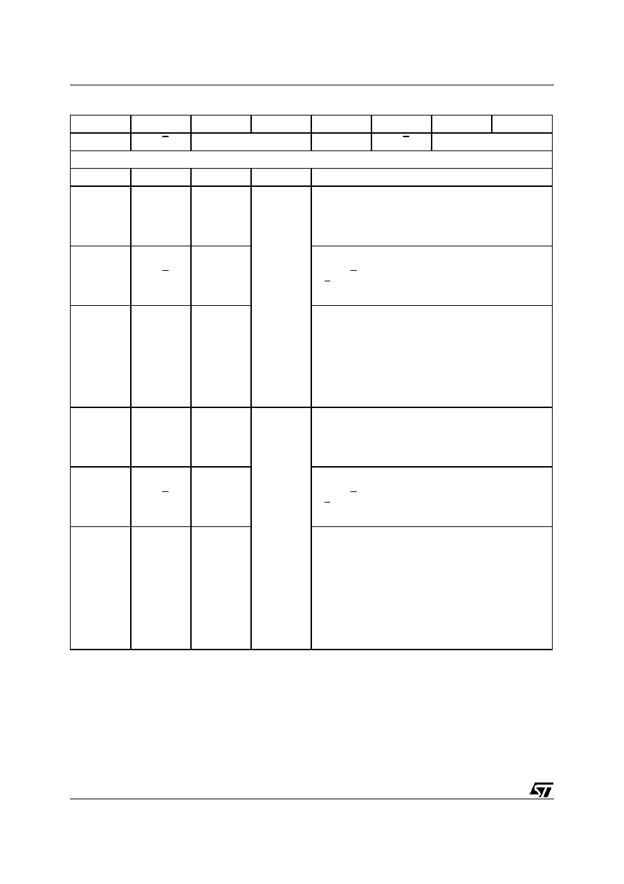
uPSD34xx - STANDARD 8032 TIMER/COUNTERS
74/264
Table 42. TMOD: Timer Mode Register (SFR 89h, reset value 00h)
Bit 7
Bit 6
Bit 5
Bit 4
Bit 3
Bit 2
Bit 1
Bit 0
GATE
C/T
M[1:0]
GATE
C/T
M[1:0]
Details
Bit
Symbol
R/W
Timer
Definition (T/C is abbreviation for Timer/Counter)
7
GATE
R,W
Timer 1
Gate control.
When GATE = 1, T/C is enabled only while pin EXTINT1
is '1' and the flag TR1 is '1.' When GATE = 0, T/C is
enabled whenever the flag TR1 is '1.'
6
C/T
R,W
Counter or Timer function select.
When C/T = 0, function is timer, clocked by internal clock.
C/T = 1, function is counter, clocked by signal sampled on
external pin, C1.
[5:4]
M[1:0]
R,W
Mode Select.
00b = 13-bit T/C. 8 bits in TH1 with TL1 as 5-bit pre-
scaler.
01b = 16-bit T/C. TH1 and TL1 are cascaded. No pre-
scaler.
10b = 8-bit auto-reload T/C. TH1 holds a constant and
loads into TL1 upon overflow.
11b = Timer Counter 1 is stopped.
3
GATE
R,W
Timer 0
Gate control.
When GATE = 1, T/C is enabled only while pin EXTINT0
is '1' and the flag TR0 is '1.' When GATE = 0, T/C is
enabled whenever the flag TR0 is '1.'
2
C/T
R,W
Counter or Timer function select.
When C/T = 0, function is timer, clocked by internal clock.
C/T = 1, function is counter, clocked by signal sampled on
external pin, C0.
[1:0]
M[1:0]
R,W
Mode Select.
00b = 13-bit T/C. 8 bits in TH0 with TL0 as 5-bit pre-
scaler.
01b = 16-bit T/C. TH0 and TL0 are cascaded. No pre-
scaler.
10b = 8-bit auto-reload T/C. TH0 holds a constant and
loads into TL0 upon overflow.
11b = TL0 is 8-bit T/C controlled by standard Timer 0
control bits. TH0 is a separate 8-bit timer that uses Timer
1 control bits.
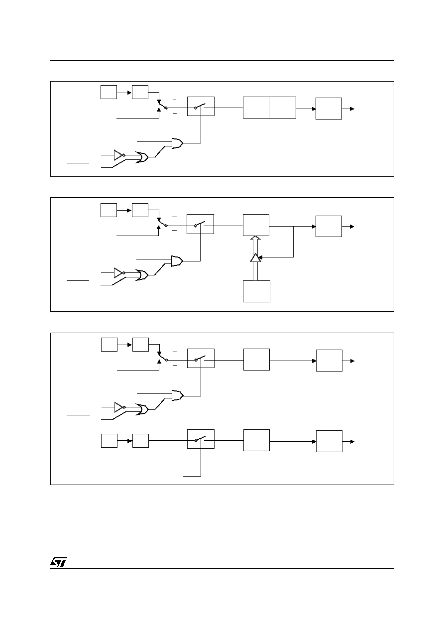
75/264
uPSD34xx - STANDARD 8032 TIMER/COUNTERS
Figure 25. Timer/Counter Mode 0: 13-bit Counter
Figure 26. Timer/Counter Mode 2: 8-bit Auto-reload
Figure 27. Timer/Counter Mode 3: Two 8-bit Counters
AI06622
f
OSC
TF1
Interrupt
Gate
TR1
EXTINT1 pin
C1 pin
Control
TL1
(5 bits)
TH1
(8 bits)
C/T = 0
C/T = 1
˜ 12
AI06623
f
OSC
TF1
Interrupt
Gate
TR1
EXTINT1 pin
C1 pin
Control
TL1
(8 bits)
TH1
(8 bits)
C/T = 0
C/T = 1
˜ 12
AI06624
f
OSC
TF0
Interrupt
Gate
TR0
EXTINT0 pin
C0 pin
Control
TL0
(8 bits)
C/T = 0
C/T = 1
˜ 12
f
OSC
TF1
Interrupt
Control
TH0
(8 bits)
˜ 12
TR1

uPSD34xx - STANDARD 8032 TIMER/COUNTERS
76/264
Timer 2
Timer 2 can operate as either an event timer or as
an event counter. This is selected by the bit C/T2
in the SFR named, T2CON (
Table 43., page 77
).
Timer 2 has three operating modes selected by
bits in T2CON, according to
Table 44., page 78
.
The three modes are:
Capture mode
Auto re-load mode
Baud rate generator mode
Capture Mode. In Capture Mode there are two
options which are selected by the bit EXEN2 in
T2CON.
Figure 28., page 81
illustrates Capture
mode.
If EXEN2 = 0, then Timer 2 is a 16-bit timer if C/T2
= 0, or it is a 16-bit counter if C/T2 = 1, either of
which sets the interrupt flag bit TF2 upon overflow.
If EXEN2 = 1, then Timer 2 still does the above,
but with the added feature that a 1-to-0 transition
at external input pin T2X causes the current value
in the Timer 2 registers, TL2 and TH2, to be cap-
tured into Registers RCAP2L and RCAP2H, re-
spectively. In addition, the transition at T2X
causes interrupt flag bit EXF2 in T2CON to be set.
Either flag TF2 or EXF2 will generate an interrupt
and the MCU must read both flags to determine
the cause. Flags TF2 and EXF2 are not automati-
cally cleared by hardware, so the firmware servic-
ing the interrupt must clear the flag(s) upon exit of
the interrupt service routine.
Auto-reload Mode. In the Auto-reload Mode,
there are again two options, which are selected by
the bit EXEN2 in T2CON.
Figure 29., page 81
shows Auto-reload mode.
If EXEN2 = 0, then when Timer 2 counts up and
rolls over from FFFFh it not only sets the interrupt
flag TF2, but also causes the Timer 2 registers to
be reloaded with the 16-bit value contained in
Registers RCAP2L and RCAP2H, which are pre-
set with firmware.
If EXEN2 = 1, then Timer 2 still does the above,
but with the added feature that a 1-to-0 transition
at external input T2X will also trigger the 16-bit re-
load and set the interrupt flag EXF2. Again, firm-
ware servicing the interrupt must read both TF2
and EXF2 to determine the cause, and clear the
flag(s) upon exit.
Note: The uPSD34xx does not support selectable
up/down counting in Auto-reload mode (this fea-
ture was an extension to the original 8032 archi-
tecture).
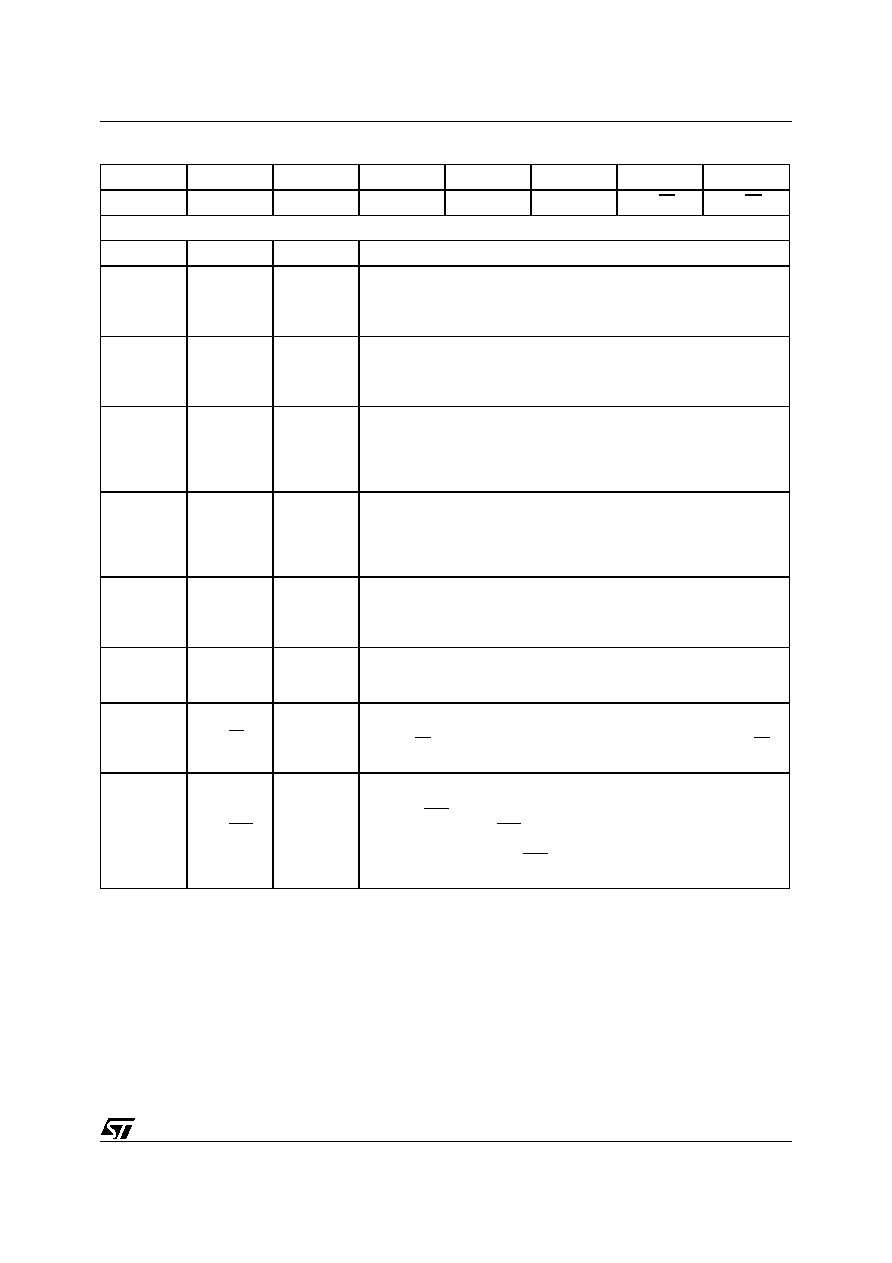
77/264
uPSD34xx - STANDARD 8032 TIMER/COUNTERS
Table 43. T2CON: Timer 2 Control Register (SFR C8h, reset value 00h)
Note: 1. The RCLK1 and TCLK1 Bits in the SFR named PCON control UART1, and have the exact same function as RCLK and TCLK.
Bit 7
Bit 6
Bit 5
Bit 4
Bit 3
Bit 2
Bit 1
Bit 0
TF2
EXF2
RCLK
TCLK
EXEN2
TR2
C/T2
CP/RL2
Details
Bit
Symbol
R/W
Definition
7
TF2
R,W
Timer 2 flag, causes interrupt if enabled.
TF2 is set by hardware upon overflow. Must be cleared by firmware. TF2
will not be set when either RCLK or TCLK =1.
6
EXF2
R,W
Timer 2 flag, causes interrupt if enabled.
EXF2 is set when a capture or reload is caused by a negative transition
on T2X pin and EXEN2 = 1. EXF2 must be cleared by firmware.
5
RCLK
(1)
R,W
UART0 Receive Clock control.
When RCLK = 1, UART0 uses Timer 2 overflow pulses for its receive
clock in Modes 1 and 3. RCLK=0, Timer 1 overflow is used for its receive
clock
4
TCLK
(1)
R,W
UART0 Transmit Clock control.
When TCLK = 1, UART0 uses Timer 2 overflow pulses for its transmit
clock in Modes 1 and 3. TCLK=0, Timer 1 overflow is used for transmit
clock
3
EXEN2
R,W
Timer 2 External Enable.
When EXEN2 = 1, capture or reload results when negative edge on pin
T2X occurs. EXEN2 = 0 causes Timer 2 to ignore events at pin T2X.
2
TR2
R,W
Timer 2 run control.
1 = Timer/Counter 2 is on, 0 = Timer Counter 2 is off.
1
C/T2
R,W
Counter or Timer function select.
When C/T2 = 0, function is timer, clocked by internal clock. When C/T2 =
1, function is counter, clocked by signal sampled on external pin, T2.
0
CP/RL2
R,W
Capture/Reload.
When CP/RL2 = 1, capture occurs on negative transition at pin T2X if
EXEN2 = 1. When CP/RL2 = 0, auto-reload occurs when Timer 2
overflows, or on negative transition at pin T2X when EXEN2=1. When
RCLK = 1 or TCLK = 1, CP/RL2 is ignored, and Timer 2 is forced to auto-
reload upon Timer 2 overflow
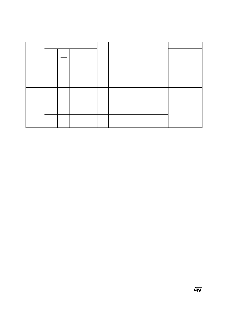
uPSD34xx - STANDARD 8032 TIMER/COUNTERS
78/264
Table 44. Timer/Counter 2 Operating Modes
Note:
= falling edge
Mode
Bits in T2CON SFR
Pin
T2X
Remarks
Input Clock
RCLK
or
TCLK
CP/
RL2
TR2
EXEN2
Timer,
Internal
Counter,
External
(Pin T2,
P1.0)
16-bit
Auto-
reload
0
0
1
0
x
reload [RCAP2H, RCAP2L] to [TH2,
TL2] upon overflow (up counting)
f
OSC
/12
MAX
f
OSC
/24
0
0
1
1
reload [RCAP2H, RCAP2L] to [TH2,
TL2] at falling edge on pin T2X
16-bit
Capture
0
1
1
0
x
16-bit Timer/Counter (up counting)
f
OSC
/12
MAX
f
OSC
/24
0
1
1
1
Capture [TH2, TL2] and store to
[RCAP2H, RCAP2L] at falling edge on
pin T2X
Baud Rate
Generator
1
x
1
0
x
No overflow interrupt request (TF2)
f
OSC
/2
≠
1
x
1
1
Extra Interrupt on pin T2X, sets TF2
Off
x
x
0
x
x
Timer 2 stops
≠
≠

79/264
uPSD34xx - STANDARD 8032 TIMER/COUNTERS
Baud Rate Generator Mode. The RCLK and/or
TCLK Bits in the SFR T2CON allow the transmit
and receive baud rates on serial port UART0 to be
derived from either Timer 1 or Timer 2.
Figure
30., page 82
illustrates Baud Rate Generator
Mode.
When TCLK = 0, Timer 1 is used as UART0's
transmit baud generator. When TCLK = 1, Timer 2
will be the transmit baud generator. RCLK has the
same effect for UART0's receive baud rate. With
these two bits, UART0 can have different receive
and transmit baud rates - one generated by Timer
1, the other by Timer 2.
Note: Bits RCLK1 and TCLK1 in the SFR named
PCON (see
PCON: Power Control Register (SFR
87h, reset value 00h), page 52
) have identical
functions as RCLK and TCLK but they apply to
UART1 instead. For simplicity in the following dis-
cussions about baud rate generation, no suffix will
be used when referring to SFR registers and bits
related to UART0 or UART1, since each UART in-
terface has identical operation. Example, TCLK or
TCLK1 will be referred to as just TCLK.
The Baud Rate Generator Mode is similar to the
Auto-reload Mode, in that a roll over in TH2 causes
the Timer 2 registers, TH2 and TL2, to be reloaded
with the 16-bit value in Registers RCAP2H and
RCAP2L, which are preset with firmware.
The baud rates in UART Modes 1 and 3 are deter-
mined by Timer 2's overflow rate as follows:
UART Mode 1,3 Baud Rate =
Timer 2 Overflow Rate / 16
The timer can be configured for either "timer" or
"counter" operation. In the most typical applica-
tions, it is configured for "timer" operation (C/T2 =
0). "Timer" operation is a little different for Timer 2
when it's being used as a baud rate generator. In
this case, the baud rate is given by the formula:
UART Mode 1,3 Baud Rate =
f
OSC
/(32 x [65536 ≠ [RCAP2H, RCAP2L]))
where [RCAP2H, RCAP2L] is the content of the
SFRs RCAP2H and RCAP2L taken as a 16-bit un-
signed integer.
A roll-over in TH2 does not set TF2, and will not
generate an interrupt. Therefore, the Timer Inter-
rupt does not have to be disabled when Timer 2 is
in the Baud Rate Generator Mode.
If EXEN2 is set, a 1-to-0 transition on pin T2X will
set the Timer 2 interrupt flag EXF2, but will not
cause a reload from RCAP2H and RCAP2L to
TH2 and TL2. Thus when Timer 2 is in use as a
baud rate generator, the pin T2X can be used as
an extra external interrupt, if desired.
When Timer 2 is running (TR2 = 1) in a "timer"
function in the Baud Rate Generator Mode, firm-
ware should not read or write TH2 or TL2. Under
these conditions the results of a read or write may
not be accurate. However, SFRs RCAP2H and
RCAP2L may be read, but should not be written,
because a write might overlap a reload and cause
write and/or reload errors. Timer 2 should be
turned off (clear TR2) before accessing Timer 2 or
Registers RCAP2H and RCAP2L, in this case.
Table 45., page 80
shows commonly used baud
rates and how they can be obtained from Timer 2,
with T2CON = 34h.

uPSD34xx - STANDARD 8032 TIMER/COUNTERS
80/264
Table 45. Commonly Used Baud Rates Generated from Timer2 (T2CON = 34h)
f
OSC
MHz
Desired
Baud Rate
Timer 2 SFRs
Resulting
Baud Rate
Baud Rate
Deviation
RCAP2H (hex)
RCAP2L(hex)
40.0 115200
FF
F5
113636
-1.36%
40.0 57600
FF
EA
56818
-1.36%
40.0
28800
FF
D5
29070
0.94%
40.0 19200
FF
BF
19231
0.16%
40.0
9600
FF
7E
9615
0.16%
36.864
115200
FF
F6
115200
0
36.864
57600
FF
EC
57600
0
36.864
28800
FF
D8
28800
0
36.864
19200
FF
C4
19200
0
36.864
9600
FF
88
9600
0
36.0
28800
FF
D9
28846
0.16%
36.0
19200
FF
C5
19067
-0.69%
36.0
9600
FF
8B
9615
0.16%
24.0
57600
FF
F3
57692
0.16%
24.0
28800
FF
E6
28846
0.16%
24.0
19200
FF
D9
19231
0.16%
24.0
9600
FF
B2
9615
0.16%
12.0
28800
FF
F3
28846
0.16%
12.0
9600
FF
D9
9615
0.16%
11.0592
115200
FF
FD
115200
0
11.0592
57600
FF
FA
57600
0
11.0592
28800
FF
F4
28800
0
11.0592
19200
FF
EE
19200
0
11.0592
9600
FF
DC
9600
0
3.6864
115200
FF
FF
115200
0
3.6864
57600
FF
FE
57600
0
3.6864
28800
FF
FC
28800
0
3.6864
19200
FF
FA
19200
0
3.6864
9600
FF
F4
9600
0
1.8432
19200
FF
FD
19200
0
1.8432
9600
FF
FA
9600
0

81/264
uPSD34xx - STANDARD 8032 TIMER/COUNTERS
Figure 28. Timer 2 in Capture Mode
Figure 29. Timer 2 in Auto-Reload Mode
AI06625
f
OSC
TF2
Capture
TR2
T2 pin
Control
TL2
(8 bits)
TH2
(8 bits)
C/T2 = 0
C/T2 = 1
˜ 12
EXP2
Control
EXEN2
RCAP2L RCAP2H
T2X pin
Timer 2
Interrupt
Transition
Detector
AI06626
f
OSC
TF2
Reload
TR2
T2 pin
Control
TL2
(8 bits)
TH2
(8 bits)
C/T2 = 0
C/T2 = 1
˜ 12
EXP2
Control
EXEN2
RCAP2L RCAP2H
T2X pin
Timer 2
Interrupt
Transition
Detector
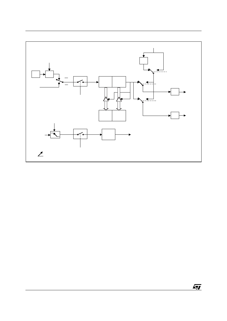
uPSD34xx - STANDARD 8032 TIMER/COUNTERS
82/264
Figure 30. Timer 2 in Baud Rate Generator Mode
AI09605
f
OSC
Reload
TR2
T2 pin
Control
Note: Oscillator frequency is divided by 2,
not 12 like in other timer modes.
Note: Availability of additional external interrupt.
TL2
(8 bits)
TH2
(8 bits)
C/T2 = 0
C/T2 = 1
˜ 12
˜ 2
˜ 16
˜ 16
EXF2
Control
EXEN2
RCAP2L RCAP2H
T2X pin
Timer 2 Interrupt
TX CLK
RX CLK
Timer 1 Overflow
SMOD
RCLK
'1'
'0'
'1'
'0'
'1'
'0'
TCLK
Transition
Detector

83/264
uPSD34xx - SERIAL UART INTERFACES
SERIAL UART INTERFACES
uPSD34xx devices provide two standard 8032
UART serial ports.
≠
The first port, UART0, is connected to pins
RxD0 (P3.0) and TxD0 (P3.1)
≠
The second port, UART1 is connected to pins
RxD1 (P1.2) and TxD1 (P1.3). UART1 can
optionally be routed to pins P4.2 and P4.3 as
described in
Alternate Functions, page 60
.
The operation of the two serial ports are the same
and are controlled by two SFRs:
SCON0 (
Table 47., page 84
) for UART0
SCON1 (
Table 48., page 85
) for UART1
Each UART has its own data buffer accessed
through an SFR listed below:
SBUF0 for UART0, address 99h
SBUF1 for UART1, address D9h
When writing SBU0 or SBUF1, the data automati-
cally loads into the associated UART transmit data
register. When reading this SFR, data comes from
a different physical register, which is the receive
register of the associated UART.
Note: For simplicity in the remaining UART dis-
cussions, the suffix "0" or "1" will be dropped when
referring to SFR registers and bits related to
UART0 or UART1, since each UART interface has
identical operation. Example, SBUF0 and SBUF1
will be referred to as just SBUF.
Each UART serial port can be full-duplex, meaning
it can transmit and receive simultaneously. Each
UART is also receive-buffered, meaning it can
commence reception of a second byte before a
previously received byte has been read from the
SBUF Register. However, if the first byte still has
not been read by the time reception of the second
byte is complete, one of the bytes will be lost.
UART Operation Modes
Each UART can operate in one of four modes, one
mode is synchronous, and the others are asyn-
chronous as shown in Table
46
.
Mode 0. Mode 0 provides asynchronous, half-du-
plex operation. Serial data is both transmitted, and
received on the RxD pin. The TxD pin outputs a
shift clock for both transmit and receive directions,
thus the MCU must be the master. Eight bits are
transmitted/received LSB first. The baud rate is
fixed at 1/12 of f
OSC
.
Mode 1. Mode 1 provides standard asynchro-
nous, full-duplex communication using a total of 10
bits per data byte. Data is transmitted through TxD
and received through RxD with: a Start Bit (logic
'0'), eight data bits (LSB first), and a Stop Bit (logic
'1'). Upon receive, the eight data bits go into the
SFR SBUF, and the Stop Bit goes into bit RB8 of
the SFR SCON. The baud rate is variable and de-
rived from overflows of Timer 1 or Timer 2.
Mode 2. Mode 2 provides asynchronous, full-du-
plex communication using a total of 11 bits per
data byte. Data is transmitted through TxD and re-
ceived through RxD with: a Start Bit (logic '0');
eight data bits (LSB first); a programmable 9th
data bit; and a Stop Bit (logic '1'). Upon Transmit,
the 9th data bit (from bit TB8 in SCON) can be as-
signed the value of '0' or '1.' Or, for example, the
Parity Bit (P, in the PSW) could be moved into
TB8. Upon receive, the 9th data bit goes into RB8
in SCON, while the Stop Bit is ignored. The baud
rate is programmable to either 1/32 or 1/64 of
f
OSC
.
Mode 3. Mode 3 is the same as Mode 2 in all re-
spects except the baud rate is variable like it is in
Mode 1.
In all four modes, transmission is initiated by any
instruction that uses SBUF as a destination regis-
ter. Reception is initiated in Mode 0 by the condi-
tion RI = 0 and REN = 1. Reception is initiated in
the other modes by the incoming Start Bit if
REN = 1.
Table 46. UART Operating Modes
Mode
Synchronization
Bits of SFR,
SCON
Baud Clock
Data
Bits
Start/Stop Bits
See Figure
SM0
SM1
0
Synchronous
0
0
f
OSC
/12
8
None
Figure
31., page 88
1
Asynchronous
0
1
Timer 1 or Timer 2 Overflow
8
1 Start, 1 Stop
Figure
33., page 90
2
Asynchronous
1
0
f
OSC
/32 or f
OSC
/64
9
1 Start, 1 Stop
Figure
35., page 92
3
Asynchronous
1
1
Timer 1 or Timer 2 Overflow
9
1 Start, 1 Stop
Figure
37., page 93
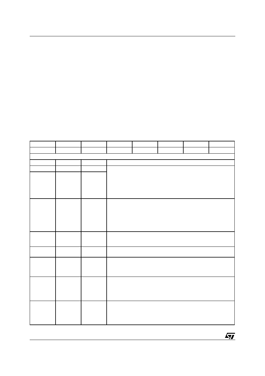
uPSD34xx - SERIAL UART INTERFACES
84/264
Multiprocessor Communications. Modes 2 and
3 have a special provision for multiprocessor com-
munications. In these modes, 9 data bits are re-
ceived. The 9th one goes into bit RB8, then comes
a stop bit. The port can be programmed such that
when the stop bit is received, the UART interrupt
will be activated only if bit RB8 = 1. This feature is
enabled by setting bit SM2 in SCON. A way to use
this feature in multi-processor systems is as fol-
lows: When the master processor wants to trans-
mit a block of data to one of several slaves, it first
sends out an address byte which identifies the tar-
get slave. An address byte differs from a data byte
in that the 9th bit is 1 in an address byte and 0 in a
data byte. With SM2 = 1, no slave will be interrupt-
ed by a data byte. An address byte, however, will
interrupt all slaves, so that each slave can exam-
ine the received byte and see if it is being ad-
dressed. The addressed slave will clear its SM2 bit
and prepare to receive the data bytes that will be
coming. The slaves that were not being addressed
leave their SM2 bits set and go on about their busi-
ness, ignoring the coming data bytes.
SM2 has no effect in Mode 0, and in Mode 1, SM2
can be used to check the validity of the stop bit. In
a Mode 1 reception, if SM2 = 1, the receive inter-
rupt will not be activated unless a valid stop bit is
received.
Serial Port Control Registers
The SFR SCON0 controls UART0, and SCON1
controls UART1, shown in Table
47
and Table
48
.
These registers contain not only the mode selec-
tion bits, but also the 9th data bit for transmit and
receive (bits TB8 and RB8), and the UART Inter-
rupt flags, TI and RI.
Table 47. SCON0: Serial Port UART0 Control Register (SFR 98h, reset value 00h)
Bit 7
Bit 6
Bit 5
Bit 4
Bit 3
Bit 2
Bit 1
Bit 0
SM0
SM1
SM2
REN
TB8
RB8
TI
RI
Details
Bit
Symbol
R/W
Definition
7
SM0
R,W
Serial Mode Select, See
Table 46., page 83
. Important, notice bit order
of SM0 and SM1.
[SM0:SM1] = 00b, Mode 0
[SM0:SM1] = 01b, Mode 1
[SM0:SM1] = 10b, Mode 2
[SM0:SM1] = 11b, Mode 3
6
SM1
R,W
5
SM2
R,W
Serial Multiprocessor Communication Enable.
Mode 0: SM2 has no effect but should remain 0.
Mode 1: If SM2 = 0 then stop bit ignored. SM2 =1 then RI active if stop
bit = 1.
Mode 2 and 3: Multiprocessor Comm Enable. If SM2=0, 9th bit is
ignored. If SM2=1, RI active when 9th bit = 1.
4
REN
R,W
Receive Enable.
If REN=0, UART reception disabled. If REN=1, reception is enabled
3
TB8
R,W
TB8 is assigned to the 9th transmission bit in Mode 2 and 3. Not used in
Mode 0 and 1.
2
RB8
R,W
Mode 0: RB8 is not used.
Mode 1: If SM2 = 0, the RB8 is the level of the received stop bit.
Mode 2 and 3: RB8 is the 9th data bit that was received in Mode 2 and
3.
1
TI
R,W
Transmit Interrupt flag.
Causes interrupt at end of 8th bit time when transmitting in Mode 0, or at
beginning of stop bit transmission in other modes. Must clear flag with
firmware.
0
RI
R,W
Receive Interrupt flag.
Causes interrupt at end of 8th bit time when receiving in Mode 0, or
halfway through stop bit reception in other modes (see SM2 for
exception). Must clear this flag with firmware.

85/264
uPSD34xx - SERIAL UART INTERFACES
Table 48. SCON1: Serial Port UART1 Control Register (SFR D8h, reset value 00h)
Bit 7
Bit 6
Bit 5
Bit 4
Bit 3
Bit 2
Bit 1
Bit 0
SM0
SM1
SM2
REN
TB8
RB8
TI
RI
Details
Bit
Symbol
R/W
Definition
7
SM0
R,W
Serial Mode Select, See
Table 46., page 83
. Important, notice bit order
of SM0 and SM1.
[SM0:SM1] = 00b, Mode 0
[SM0:SM1] = 01b, Mode 1
[SM0:SM1] = 10b, Mode 2
[SM0:SM1] = 11b, Mode 3
6
SM1
R,W
5
SM2
R,W
Serial Multiprocessor Communication Enable.
Mode 0: SM2 has no effect but should remain 0.
Mode 1: If SM2 = 0 then stop bit ignored. SM2 =1 then RI active if stop
bit = 1.
Mode 2 and 3: Multiprocessor Comm Enable. If SM2=0, 9th bit is
ignored. If SM2=1, RI active when 9th bit = 1.
4
REN
R,W
Receive Enable.
If REN=0, UART reception disabled. If REN=1, reception is enabled
3
TB8
R,W
TB8 is assigned to the 9th transmission bit in Mode 2 and 3. Not used in
Mode 0 and 1.
2
RB8
R,W
Mode 0: RB8 is not used.
Mode 1: If SM2 = 0, the RB8 is the level of the received stop bit.
Mode 2 and 3: RB8 is the 9th data bit that was received in Mode 2 and
3.
1
TI
R,W
Transmit Interrupt flag.
Causes interrupt at end of 8th bit time when transmitting in Mode 0, or at
beginning of stop bit transmission in other modes. Must clear flag with
firmware.
0
RI
R,W
Receive Interrupt flag.
Causes interrupt at end of 8th bit time when receiving in Mode 0, or
halfway through stop bit reception in other modes (see SM2 for
exception). Must clear this flag with firmware.
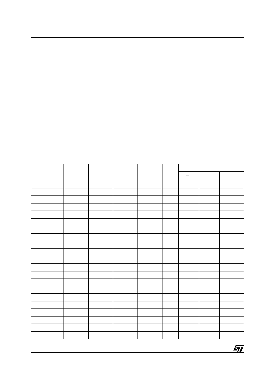
uPSD34xx - SERIAL UART INTERFACES
86/264
UART Baud Rates
The baud rate in Mode 0 is fixed:
Mode 0 Baud Rate = f
OSC
/ 12
The baud rate in Mode 2 depends on the value of
the bit SMOD in the SFR named PCON. If SMOD
= 0 (default value), the baud rate is 1/64 the oscil-
lator frequency, f
OSC
. If SMOD = 1, the baud rate
is 1/32 the oscillator frequency.
Mode 2 Baud Rate = (2
SMOD
/ 64) x f
OSC
Baud rates in Modes 1 and 3 are determined by
the Timer 1 or Timer 2 overflow rate.
Using Timer 1 to Generate Baud Rates. When
Timer 1 is used as the baud rate generator (bits
RCLK = 0, TCLK = 0), the baud rates in Modes 1
and 3 are determined by the Timer 1 overflow rate
and the value of SMOD as follows:
Mode 1,3 Baud Rate =
(2
SMOD
/ 32) x (Timer 1 overflow rate)
The Timer 1 Interrupt should be disabled in this
application. The Timer itself can be configured for
either "timer" or "counter" operation, and in any of
its 3 running modes. In the most typical applica-
tions, it is configured for "timer" operation, in the
Auto-reload Mode (high nibble of the SFR TMOD
= 0010B). In that case the baud rate is given by the
formula:
Mode 1,3 Baud Rate =
(2
SMOD
/ 32) x (f
OSC
/ (12 x [256 ≠ (TH1)]))
Table
49
lists various commonly used baud rates
and how they can be obtained from Timer 1.
Using Timer/Counter 2 to Generate Baud
Rates. See
Baud Rate Generator
Mode, page 79
.
Table 49. Commonly Used Baud Rates Generated from Timer 1
UART Mode
f
OSC
MHz
Desired
Baud Rate
Resultant
Baud Rate
Baud Rate
Deviation
SMOD
bit in
PCON
Timer 1
C/T Bit
in TMOD
Timer
Mode in
TMOD
TH1
Reload
value (hex)
Mode 0 Max
40.0
3.33MHz
3.33MHz
0
X
X
X
X
Mode 2 Max
40.0
1250 k
1250 k
0
1
X
X
X
Mode 2 Max
40.0
625 k
625 k
0
0
X
X
X
Modes 1 or 3
40.0
19200
18939
-1.36%
1
0
2
F5
Modes 1 or 3
40.0
9600
9470
-1.36%
1
0
2
EA
Modes 1 or 3
36.0
19200
18570
-2.34%
1
0
2
F6
Modes 1 or 3
33.333
57600
57870
0.47%
1
0
2
FD
Modes 1 or 3
33.333
28800
28934
0.47%
1
0
2
FA
Modes 1 or 3
33.333
19200
19290
0.47%
1
0
2
F7
Modes 1 or 3
33.333
9600
9645
0.47%
1
0
2
EE
Modes 1 or 3
24.0
9600
9615
0.16%
1
0
2
F3
Modes 1 or 3
12.0
4800
4808
0.16%
1
0
2
F3
Modes 1 or 3
11.0592
57600
57600
0
1
0
2
FF
Modes 1 or 3
11.0592
28800
28800
0
1
0
2
FE
Modes 1 or 3
11.0592
19200
19200
0
1
0
2
FD
Modes 1 or 3
11.0592
9600
9600
0
1
0
2
FA
Modes 1 or 3
3.6864
19200
19200
0
1
0
2
FF
Modes 1 or 3
3.6864
9600
9600
0
1
0
2
FE
Modes 1 or 3
1.8432
9600
9600
0
1
0
2
FF
Modes 1 or 3
1.8432
4800
4800
0
1
0
2
FE

87/264
uPSD34xx - SERIAL UART INTERFACES
More About UART Mode 0
Refer to the block diagram in
Figure 31., page 88
,
and timing diagram in
Figure 32., page 88
.
Transmission is initiated by any instruction which
writes to the SFR named SBUF. At the end of a
write operation to SBUF, a 1 is loaded into the 9th
position of the transmit shift register and tells the
TX Control unit to begin a transmission. Transmis-
sion begins on the following MCU machine cycle,
when the "SEND" signal is active in Figure
32
.
SEND enables the output of the shift register to the
alternate function on the port containing pin RxD,
and also enables the SHIFT CLOCK signal to the
alternate function on the port containing the pin,
TxD. At the end of each SHIFT CLOCK in which
SEND is active, the contents of the transmit shift
register are shifted to the right one position.
As data bits shift out to the right, zeros come in
from the left. When the MSB of the data byte is at
the output position of the shift register, then the '1'
that was initially loaded into the 9th position, is just
to the left of the MSB, and all positions to the left
of that contain zeros. This condition flags the TX
Control unit to do one last shift, then deactivate
SEND, and then set the interrupt flag TI. Both of
these actions occur at S1P1.
Reception is initiated by the condition REN = 1 and
RI = 0. At the end of the next MCU machine cycle,
the RX Control unit writes the bits 11111110 to the
receive shift register, and in the next clock phase
activates RECEIVE. RECEIVE enables the SHIFT
CLOCK signal to the alternate function on the port
containing the pin, TxD. Each pulse of SHIFT
CLOCK moves the contents of the receive shift
register one position to the left while RECEIVE is
active. The value that comes in from the right is the
value that was sampled at the RxD pin. As data
bits come in from the right, 1s shift out to the left.
When the 0 that was initially loaded into the right-
most position arrives at the left-most position in the
shift register, it flags the RX Control unit to do one
last shift, and then it loads SBUF. After this, RE-
CEIVE is cleared, and the receive interrupt flag RI
is set.
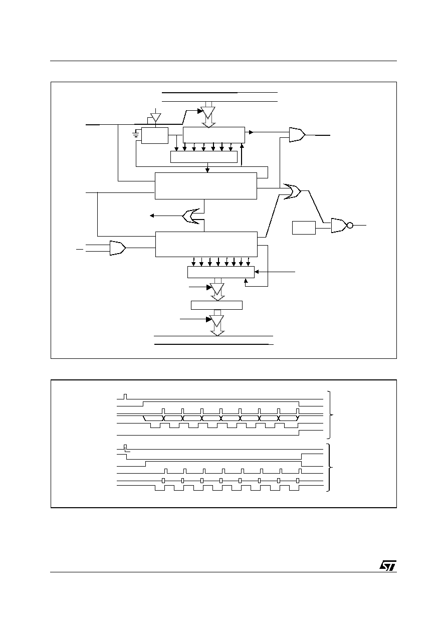
uPSD34xx - SERIAL UART INTERFACES
88/264
Figure 31. UART Mode 0, Block Diagram
Figure 32. UART Mode 0, Timing Diagram
AI06824
Zero Detector
Internal Bus
Tx Control
Rx Control
Internal Bus
SBUF
Write
to
SBUF
Read
SBUF
Load
SBUF
SBUF
Input Shift Register
Shift
Shift
Clock
Serial
Port
Interrupt
fOSC/12
REN
R1
Rx Clock
Start
Tx Clock
Start
Shift
Shift
Send
Receive
T
R
CL
D
S
Q
7 6 5 4 3 2 1 0
RxD
P3.0 Alt
Input
Function
RxD
Pin
TxD
Pin
AI06825
Write to SBUF
Send
Shift
RxD (Data Out)
TxD (Shift Clock)
TI
Write to SCON
RI
Receive
Shift
RxD (Data In)
TxD (Shift Clock)
Clear RI
Receive
Transmit
D0
D1
D2
D3
D4
D5
D6
D7
D0
D1
D2
D3
D4
D5
D6
D7

89/264
uPSD34xx - SERIAL UART INTERFACES
More About UART Mode 1
Refer to the block diagram in
Figure 33., page 90
,
and timing diagram in
Figure 34., page 90
.
Transmission is initiated by any instruction which
writes to SBUF. At the end of a write operation to
SBUF, a '1' is loaded into the 9th position of the
transmit shift register and flags the TX Control unit
that a transmission is requested. Transmission ac-
tually starts at the end of the MCU the machine cy-
cle following the next rollover in the divide-by-16
counter. Thus, the bit times are synchronized to
the divide-by-16 counter, not to the writing of
SBUF. Transmission begins with activation of
SEND which puts the start bit at pin TxD. One bit
time later, DATA is activated, which enables the
output bit of the transmit shift register to pin TxD.
The first shift pulse occurs one bit time after that.
As data bits shift out to the right, zeros are clocked
in from the left. When the MSB of the data byte is
at the output position of the shift register, then the
1 that was initially loaded into the 9th position is
just to the left of the MSB, and all positions to the
left of that contain zeros. This condition flags the
TX Control unit to do one last shift and then deac-
tivates SEND, and sets the interrupt flag, TI. This
occurs at the 10th divide-by-16 rollover after a
write to SBUF.
Reception is initiated by a detected 1-to-0 transi-
tion at the pin RxD. For this purpose RxD is sam-
pled at a rate of 16 times whatever baud rate has
been established. When a transition is detected,
the divide-by-16 counter is immediately reset, and
1FFH is written into the input shift register. Reset-
ting the divide-by-16 counter aligns its rollovers
with the boundaries of the incoming bit times. The
16 states of the counter divide each bit time into
16ths. At the 7th, 8th, and 9th counter states of
each bit time, the bit detector samples the value of
RxD. The value accepted is the value that was
seen in at least 2 of the 3 samples. This is done for
noise rejection. If the value accepted during the
first bit time is not '0,' the receive circuits are reset
and the unit goes back to looking for another '1'-to-
'0' transition. This is to provide rejection of false
start bits. If the start bit proves valid, it is shifted
into the input shift register, and reception of the re-
set of the rest of the frame will proceed. As data
bits come in from the right, '1s' shift out to the left.
When the start bit arrives at the left-most position
in the shift register (which in mode 1 is a 9-bit reg-
ister), it flags the RX Control unit to do one last
shift, load SBUF and RB8, and set the receive in-
terrupt flag RI. The signal to load SBUF and RB8,
and to set RI, will be generated if, and only if, the
following conditions are met at the time the final
shift pulse is generated:
1. RI = 0, and
2. Either SM2 = 0, or the received stop bit = 1.
If either of these two conditions are not met, the re-
ceived frame is irretrievably lost. If both conditions
are met, the stop bit goes into RB8, the 8 data bits
go into SBUF, and RI is activated. At this time,
whether the above conditions are met or not, the
unit goes back to looking for a '1'-to-'0' transition
on pin RxD.

uPSD34xx - SERIAL UART INTERFACES
90/264
Figure 33. UART Mode 1, Block Diagram
Figure 34. UART Mode 1, Timing Diagram
AI06826
Zero Detector
Internal Bus
Tx Control
Rx Control
Internal Bus
SBUF
Write
to
SBUF
Read
SBUF
Load
SBUF
SBUF
Input Shift Register
Shift
Serial
Port
Interrupt
Rx Clock
Start
Tx Clock
Start
Shift
Shift
Send
Load SBUF
TI
RI
CL
D
S
Q
1FFh
TxD
Pin
Data
Rx Detector
RxD
Pin
1-to-0
Transition
Detector
˜16
Sample
˜16
˜2
TB8
Timer1
Overflow
Timer2
Overflow
0
0
1
1
0
1
TCLK
RCLK
SMOD
AI06843
Write to SBUF
Data
Shift
TxD
TI
Rx Clock
RxD
Bit Detector
Sample Times
Shift
RI
Receive
Transmit
D0
D1
D2
D3
D4
D5
D6
D7
Send
Tx Clock
Start Bit
Stop Bit
D0
D1
D2
D3
D4
D5
D6
D7
Start Bit
Stop Bit

91/264
uPSD34xx - SERIAL UART INTERFACES
More About UART Modes 2 and 3
For Mode 2, refer to the block diagram in
Figure
35., page 92
, and timing diagram in
Figure
36., page 92
. For Mode 3, refer to the block dia-
gram in
Figure 37., page 93
, and timing diagram in
Figure 38., page 93
.
Keep in mind that the baud rate is programmable
to either 1/32 or 1/64 of f
OSC
in Mode 2, but Mode
3 uses a variable baud rate generated from Timer
1 or Timer 2 rollovers.
The receive portion is exactly the same as in Mode
1. The transmit portion differs from Mode 1 only in
the 9th bit of the transmit shift register.
Transmission is initiated by any instruction which
writes to SBUF. At the end of a write operation to
SBUF, the TB8 Bit is loaded into the 9th position of
the transmit shift register and flags the TX Control
unit that a transmission is requested. Transmis-
sion actually starts at the end of the MCU the ma-
chine cycle following the next rollover in the divide-
by-16 counter. Thus, the bit times are synchro-
nized to the divide-by-16 counter, not to the writing
of SBUF. Transmission begins with activation of
SEND which puts the start bit at pin TxD. One bit
time later, DATA is activated, which enables the
output bit of the transmit shift register to pin TxD.
The first shift pulse occurs one bit time after that.
The first shift clocks a '1' (the stop bit) into the 9th
bit position of the shift register. There-after, only
zeros are clocked in. Thus, as data bits shift out to
the right, zeros are clocked in from the left. When
bit TB8 is at the output position of the shift register,
then the stop bit is just to the left of TB8, and all po-
sitions to the left of that contain zeros. This condi-
tion flags the TX Control unit to do one last shift
and then deactivate SEND, and set the interrupt
flag, TI. This occurs at the 11th divide-by 16 roll-
over after writing to SBUF.
Reception is initiated by a detected 1-to-0 transi-
tion at pin RxD. For this purpose RxD is sampled
at a rate of 16 times whatever baud rate has been
established. When a transition is detected, the di-
vide-by-16 counter is immediately reset, and 1FFH
is written to the input shift register. At the 7th, 8th,
and 9th counter states of each bit time, the bit de-
tector samples the value of RxD. The value ac-
cepted is the value that was seen in at least 2 of
the 3 samples. If the value accepted during the
first bit time is not '0,' the receive circuits are reset
and the unit goes back to looking for another '1'-to-
'0' transition. If the start bit proves valid, it is shifted
into the input shift register, and reception of the
rest of the frame will proceed. As data bits come in
from the right, '1s' shift out to the left. When the
start bit arrives at the left-most position in the shift
register (which in Modes 2 and 3 is a 9-bit regis-
ter), it flags the RX Control unit to do one last shift,
load SBUF and RB8, and set the interrupt flag RI.
The signal to load SBUF and RB8, and to set RI,
will be generated if, and only if, the following con-
ditions are met at the time the final shift pulse is
generated:
1. RI = 0, and
2. Either SM2 = 0, or the received 9th data bit = 1.
If either of these conditions is not met, the received
frame is irretrievably lost, and RI is not set. If both
conditions are met, the received 9th data bit goes
into RB8, and the first 8 data bits go into SBUF.
One bit time later, whether the above conditions
were met or not, the unit goes back to looking for
a '1'-to-'0' transition on pin RxD.
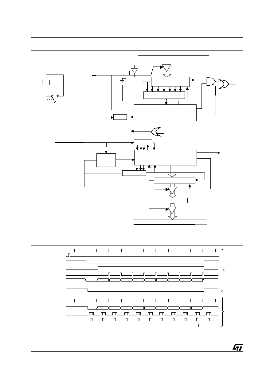
uPSD34xx - SERIAL UART INTERFACES
92/264
Figure 35. UART Mode 2, Block Diagram
Figure 36. UART Mode 2, Timing Diagram
AI06844
Zero Detector
Internal Bus
Tx Control
Rx Control
Internal Bus
SBUF
Write
to
SBUF
Read
SBUF
Load
SBUF
SBUF
Input Shift Register
Shift
Serial
Port
Interrupt
Rx Clock
Start
Tx Clock
Start
Shift
Shift
Send
Load SBUF
TI
RI
CL
D
S
Q
1FFh
TxD
Pin
Data
Rx Detector
RxD
Pin
1-to-0
Transition
Detector
˜16
Sample
˜16
˜2
TB8
fOSC/32
0
1
SMOD
AI06845
Write to SBUF
Data
Shift
TxD
TI
Rx Clock
RxD
Bit Detector
Sample Times
Shift
RI
Receive
Transmit
D0
D1
D2
D3
D4
D5
D6
D7
Send
Tx Clock
Start Bit
Stop Bit
TB8
D0
D1
D2
D3
D4
D5
D6
D7
Start Bit
Stop Bit
RB8
Stop Bit
Generator

93/264
uPSD34xx - SERIAL UART INTERFACES
Figure 37. UART Mode 3, Block Diagram
Figure 38. UART Mode 3, Timing Diagram
AI06846
Zero Detector
Internal Bus
Tx Control
Rx Control
Internal Bus
SBUF
Write
to
SBUF
Read
SBUF
Load
SBUF
SBUF
Input Shift Register
Shift
Serial
Port
Interrupt
Rx Clock
Start
Tx Clock
Start
Shift
Shift
Send
Load SBUF
TI
RI
CL
D
S
Q
1FFh
TxD
Pin
Data
Rx Detector
RxD
Pin
1-to-0
Transition
Detector
˜16
Sample
˜16
˜2
TB8
Timer1
Overflow
Timer2
Overflow
0
0
1
1
0
1
TCLK
RCLK
SMOD
AI06847
Write to SBUF
Data
Shift
TxD
TI
Rx Clock
RxD
Bit Detector
Sample Times
Shift
RI
Receive
Transmit
D0
D1
D2
D3
D4
D5
D6
D7
Send
Tx Clock
Start Bit
Stop Bit
TB8
D0
D1
D2
D3
D4
D5
D6
D7
Start Bit
Stop Bit
RB8
Stop Bit
Generator
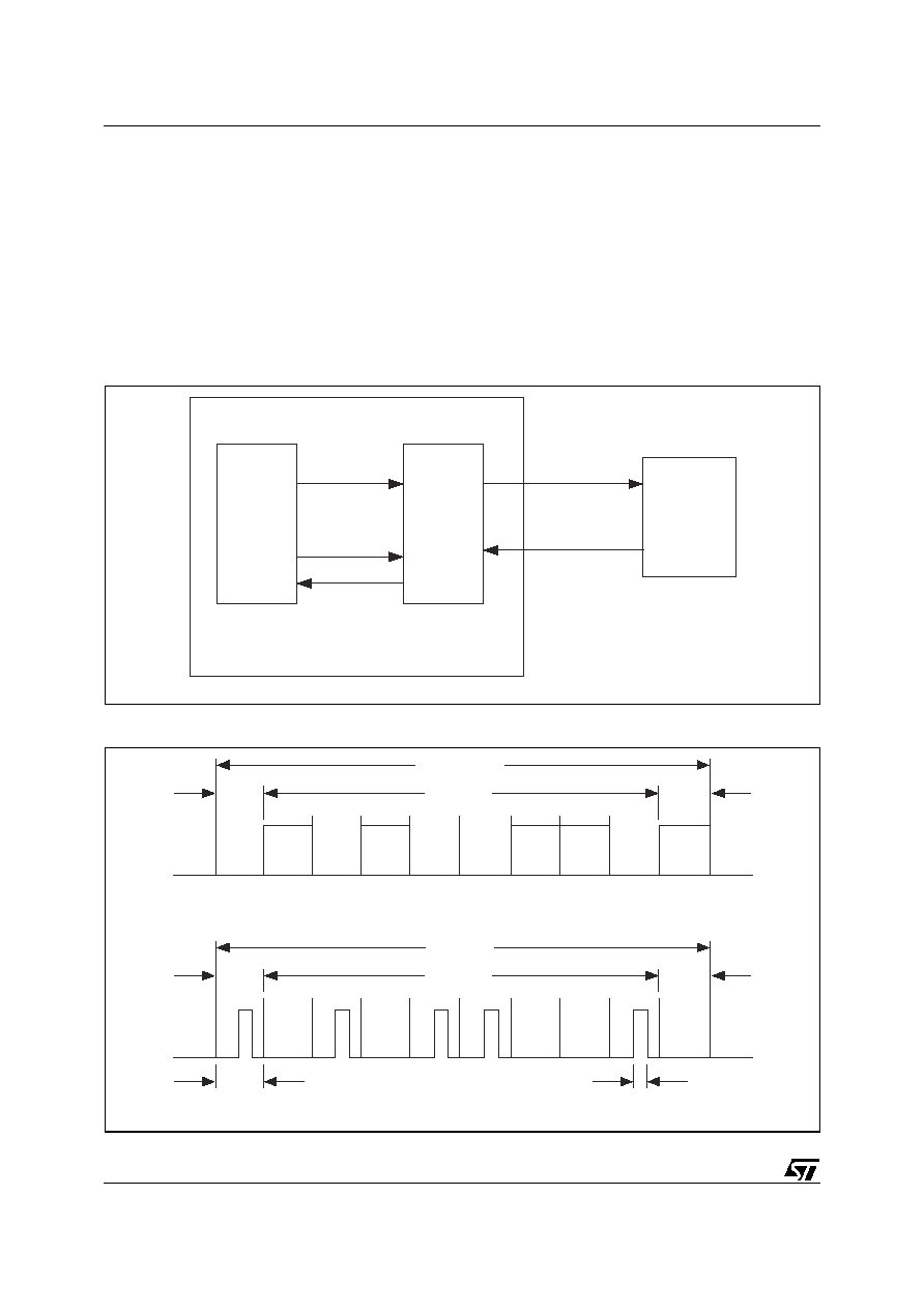
uPSD34xx - IrDA INTERFACE
94/264
IrDA INTERFACE
uPSD34xx devices provide an internal IrDA inter-
face that will allow the connection of the UART1
serial interface directly to an external infrared
transceiver device. The IrDA interface does this by
automatically shortening the pulses transmitted on
UART1's TxD1 pin, and stretching the incoming
pulses received on the RxD1 pin. Reference Fig-
ures
39
and
40
.
When the IrDA interface is enabled, the output sig-
nal from UART1's transmitter logic on pin TxD1 is
compliant with the IrDA Physical Layer Link Spec-
ification v1.4 (www.irda.org) operating from 1.2k
bps up to 115.2k bps. The pulses received on the
RxD1 pin are stretched by the IrDA interface to be
recognized by UART1's receiver logic, also adher-
ing to the IrDA specification up to 115.2k bps.
Note: In Figure
40
a logic '0' in the serial data
stream of a UART Frame corresponds to a logic
high pulse in an IR Frame. A logic '1' in a UART
Frame corresponds to no pulse in an IR Frame.
Figure 39. IrDA Interface
Figure 40. Pulse Shaping by the IrDA Interface
UART1
IrDA
Interface
TxD
RxD
uPSD34xx
IrDA
Transceiver
TxD1-IrDA
RxD1-IrDA
SIRClk
AI10437
Start
Bit
0
1
0
1
1
1
1
0
0
0
Stop
Bit
UART Frame
Data Bits
Bit Time
Pulse Width = 3/16 Bit Time
Start
Bit
0
1
0
1
1
1
1
0
0
0
Stop
Bit
UART Frame
IR Frame
IR Frame
Data Bits
AI10438
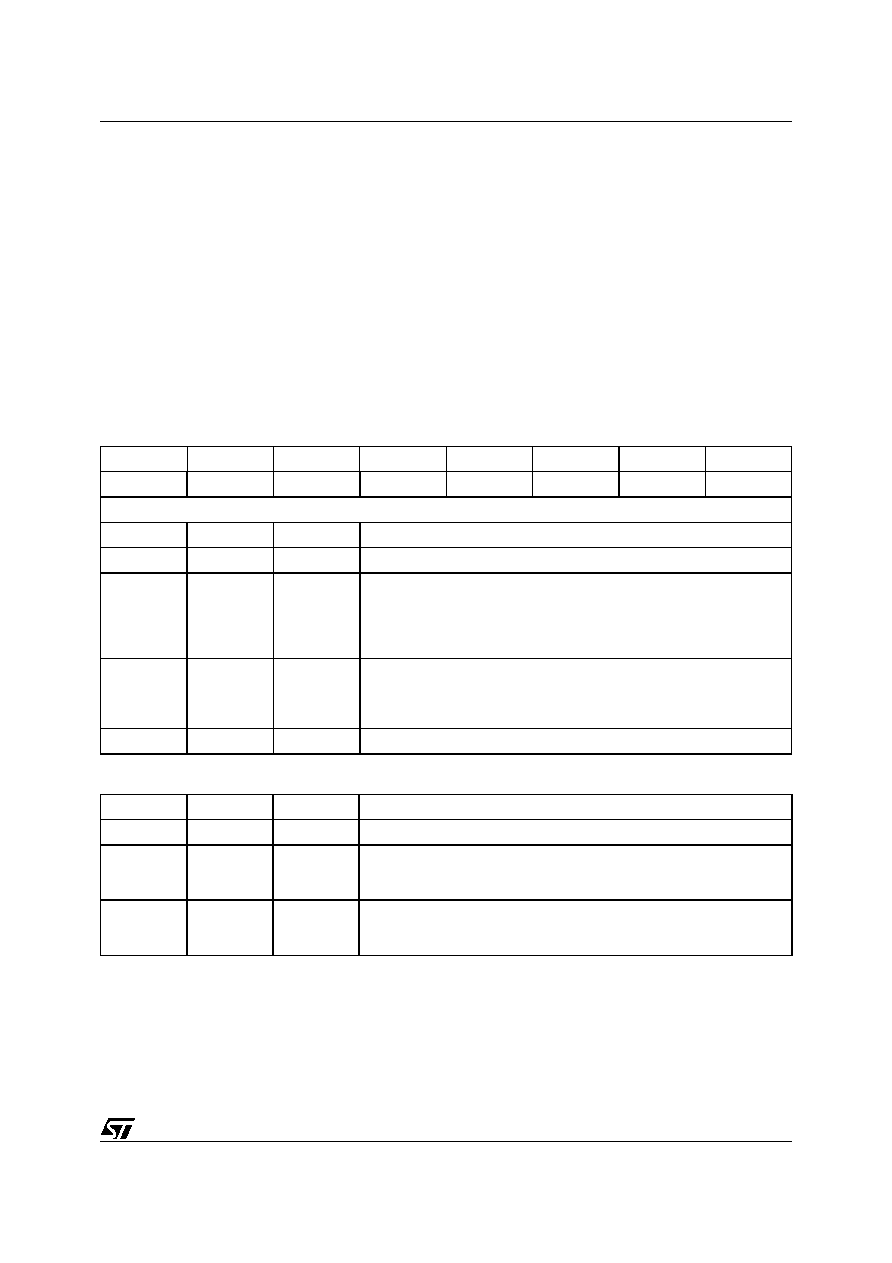
95/264
uPSD34xx - IrDA INTERFACE
The UART1 serial channel can operate in one of
four different modes as shown in
Table
46., page 83
in the section,
SERIAL UART
INTERFACES, page 83
. However, when UART1
is used for IrDA communication, UART1 must op-
erate in Mode 1 only, to be compatible with IrDA
protocol up to 115.2k bps. The IrDA interface will
support baud rates generated from Timer 1 or Tim-
er 2, just like standard UART serial communica-
tion, but with one restriction. The transmit baud
rate and receive baud rate must be the same (can-
not be different rates as is allowed by standard
UART communications).
The IrDA Interface is disabled after a reset and is
enabled by setting the IRDAEN Bit in the SFR
named IRDACON (
Table 50., page 95
). When
IrDA is disabled, the UART1's RxD and TxD sig-
nals will bypass the internal IrDA logic and instead
they are routed directly to the pins RxD1 and TxD1
respectively. When IrDA is enabled, the IrDA pulse
shaping logic is active and resides between
UART1 and the pins RxD1 and TxD1 as shown in
Figure 39., page 94
.
Baud Rate Selection
The IrDA standard only supports 2.4, 9.6, 19.2,
and 115.2kbps. Table
Table 52., page 96
informs
the IrDA Interface of the baud rate of UART#2 so
that it can perform pulse modulation properly. It
may not be necessary to implement the BR[3:0]
bits in the IRDACON Register if the IrDA Interface
obtains the proper timing from UART#2.
Table 50. IRDACON Register Bit Definition (SFR CEh, Reset Value 0Fh)
Table 51. Baud Rate Selection Register (SFR xxh, reset value xxh)
Bit 7
Bit 6
Bit 5
Bit 4
Bit 3
Bit 2
Bit 1
Bit 0
≠
IRDAEN
PULSE
CDIV4
CDIV3
CDIV2
CDIV1
CDIV0
Details
Bit
Symbol
R/W
Definition
7
≠
≠
Reserved
6
IRDAEN
RW
IrDA Enable
0 = IrDA Interface is disabled
1 = IrDA is enabled, UART1 outputs are disconnected from Port 1 (or
Port 4)
5
PULSE
RW
IrDA Pulse Modulation Select
0 = 1.627µs
1 = 3/16 bit time pulses
4-0
CDIV[4:0]
RW
Specify Clock Divider (see
Table 53., page 97
)
Bit
Symbol
R/W
Definition
7:4
BR[3:0]
R,W
Specify Baud Rate (see Table
52
)
3:2
PULSE
R,W
IrDA Pulse Modulation Select
0 = 3/16 bit time pulses (not recommended)
1 = 1.627µs
1:0
IRDAEN
R,W
0 = IrDA Interface is disabled
1 = IrDA is enabled, UART#2 outputs are disconnected from Port 1 (or
Port 4)
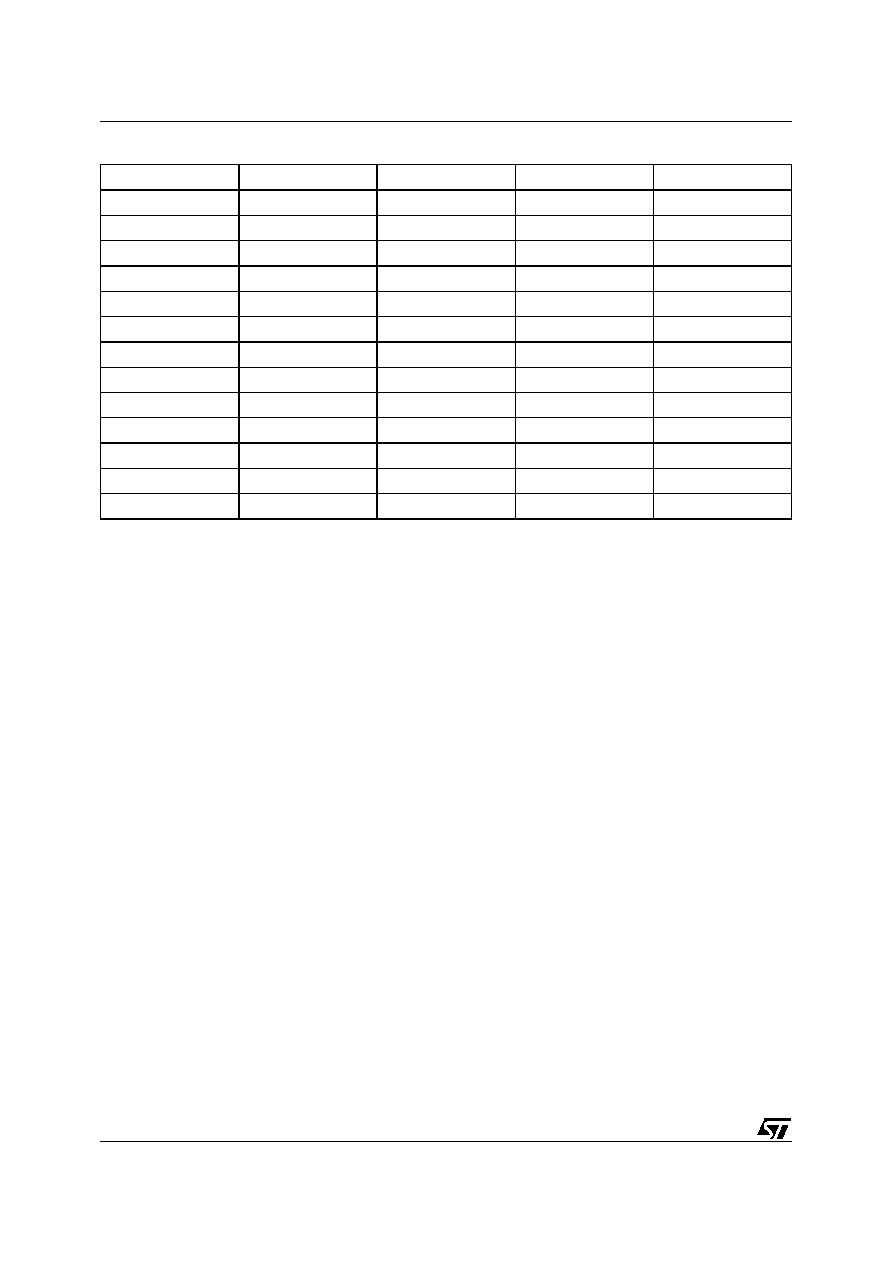
uPSD34xx - IrDA INTERFACE
96/264
Table 52. Baud Rate of UART#2 for IrDA Interface
BR3
BR2
BR1
BR0
Baud Rate (kbps)
0
0
0
0
115.2
0
0
0
1
57.5
0
0
1
0
38.4
0
0
1
1
19.2
0
1
0
0
14.4
0
1
0
1
12.8
0
1
1
0
9.6
0
1
1
1
7.2
1
0
0
0
4.8
1
0
0
1
3.6
1
0
1
0
2.4
1
0
1
1
1.8
1
1
0
0
1.2
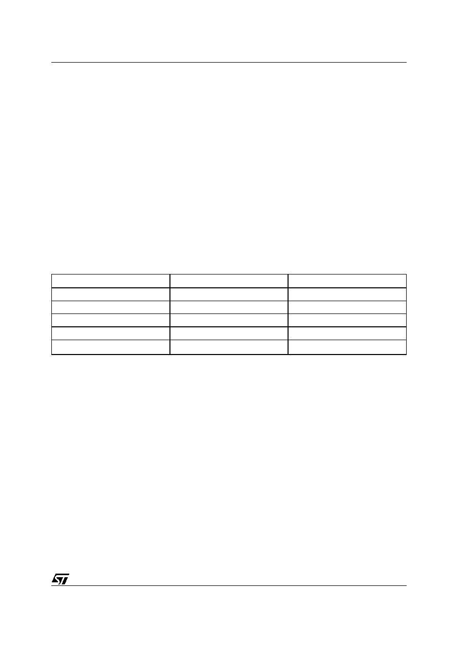
97/264
uPSD34xx - IrDA INTERFACE
Pulse Width Selection
The IrDA interface has two ways to modulate the
standard UART1 serial stream:
1.
An IrDA data pulse will have a constant pulse
width for any bit time, regardless of the
selected baud rate.
2.
An IrDA data pulse will have a pulse width that
is proportional to the the bit time of the
selected baud rate. In this case, an IrDA data
pulse width is 3/16 of its bit time, as shown in
Figure 40., page 94
.
The PULSE bit in the SFR named IRDACON de-
termines which method above will be used.
According to the IrDA physical layer specification,
for all baud rates at 115.2k bps and below, the
minimum data pulse width is 1.41µs. For a baud
rate of 115.2k bps, the maximum pulse width
2.23µs. If a constant pulse width is to be used for
all baud rates (PULSE bit = 0), the ideal general
pulse width is 1.63µs, derived from the bit time of
the fastest baud rate (8.68µs bit time for 115.2k
bps rate), multiplied by the proportion, 3/16.
To produce this fixed data pulse width when the
PULSE bit = 0, a prescaler is needed to generate
an internal reference clock, SIRClk, shown in
Fig-
ure 39., page 94
. SIRClk is derived by dividing the
oscillator clock frequency, f
OSC,
using the five bits
CDIV[4:0] in the SFR named IRDACON. A divisor
must be chosen to produce a frequency for SIRClk
that lies between 1.34 MHz and 2.13 MHz, but it is
best to choose a divisor value that produces SIR-
Clk frequency as close to 1.83MHz as possible,
because SIRClk at 1.83MHz will produce an fixed
IrDA data pulse width of 1.63µs. Table
53
provides
recommended values for CDIV[4:0] based on sev-
eral different values of f
OSC
.
For reference, SIRClk of 2.13MHz will generate a
fixed IrDA data pulse width of 1.41µs, and SIRClk
of 1.34MHz will generate a fixed data pulse width
of 2.23µs.
Table 53. Recommended CDIV[4:0] Values to Generate SIRClk (default CDIV[4:0] = 0Fh, 15 decimal)
Note: 1. When PULSE bit = 0 (fixed data pulse width), this is minimum recommended f
OSC
because CDIV[4:0] must be 4 or greater.
f
OSC
(MHz)
Value in CDIV[4:0]
Resulting f
SIRCLK
(MHz)
40.00
16h, 22 decimal
1.82
36.864, or 36.00
14h, 20 decimal
1.84, or 1.80
24.00
0Dh, 13 decimal
1.84
11.059, or 12.00
06h, 6 decimal
1.84, or 2.00
7.3728
(1)
04h, 4 decimal
1.84
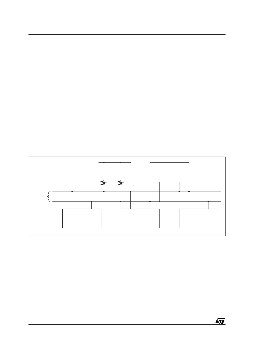
uPSD34xx - I
2
C INTERFACE
98/264
I
2
C INTERFACE
uPSD34xx devices support one serial I
2
C inter-
face. This is a two-wire communication channel,
having a bi-directional data signal (SDA, pin P3.6)
and a clock signal (SCL, pin P3.7) based on open-
drain line drivers, requiring external pull-up resis-
tors, R
P
, each with a typical value of 4.7k
(see
Figure
41
).
I
2
C Interface Main Features
Byte-wide data is transferred, MSB first, between
a Master device and a Slave device on two wires.
More than one bus Master is allowed, but only one
Master may control the bus at any given time. Data
is not lost when another Master requests the use
of a busy bus because I
2
C supports collision de-
tection and arbitration. The bus Master initiates all
data movement and generates the clock that per-
mits the transfer. Once a transfer is initiated by the
Master, any device addressed is considered a
Slave. Automatic clock synchronization allows I
2
C
devices with different bit rates to communicate on
the same physical bus. A single device can play
the role of Master or Slave, or a single device can
be a Slave only. Each Slave device on the bus has
a unique address, and a general broadcast ad-
dress is also available. A Master or Slave device
has the ability to suspend data transfers if the de-
vice needs more time to transmit or receive data.
This I
2
C interface has the following features:
≠
Serial I/O Engine (SIOE): serial/parallel
conversion; bus arbitration; clock generation
and synchronization; and handshaking are all
performed in hardware
≠
Interrupt or Polled operation
≠
Multi-master capability
≠
7-bit Addressing
≠
Supports standard speed I
2
C (SCL up to
100kHz), fast mode I
2
C (101KHz to 400kHz),
and high-speed mode I
2
C (401KHz to
833kHz)
Figure 41. Typical I
2
C Bus Configuration
Note: 1. For 3.3V system, connect R
P
to 3.3V V
CC
. For 5.0V system, connect R
P
to 5.0V V
DD
.
I2C BUS
SDA
SCL
RP
RP
VCC or VDD
(1)
Device with I2C
Interface
Device with I2C
Interface
SDA/P3.6
SCL/P3.7
uPSD33XX(V)
Device with I2C
Interface
AI09623

99/264
uPSD34xx - I
2
C INTERFACE
Communication Flow
I
2
C data flow control is based on the fact that all
I
2
C compatible devices will drive the bus lines with
open-drain (or open-collector) line drivers pulled
up with external resistors, creating a wired-AND
situation. This means that either bus line (SDA or
SCL) will be at a logic '1' level only when no I
2
C de-
vice is actively driving the line to logic '0.' The logic
for handshaking, arbitration, synchronization, and
collision detection is implemented by each I
2
C de-
vice having:
1.
The ability to hold a line low against the will of
the other devices who are trying to assert the
line high.
2.
The ability of a device to detect that another
device is driving the line low against its will.
Assert high means the driver releases the line and
external pull-ups passively raise the signal to logic
'1.' Holding low means the open-drain driver is
actively pulling the signal to ground for a logic '0.'
For example, if a Slave device cannot transmit or
receive a byte because it is distracted by and inter-
rupt or it has to wait for some process to complete,
it can hold the SCL clock line low. Even though the
Master device is generating the SCL clock, the
Master will sense that the Slave is holding the SCL
line low against the will of the Master, indicating
that the Master must wait until the Slave releases
SCL before proceeding with the transfer.
Another example is when two Master devices try
to put information on the bus simultaneously, the
first one to release the SDA data line looses arbi-
tration while the winner continues to hold SDA low.
Two types of data transfers are possible with I
2
C
depending on the R/W bit, see
Figure
42., page 100
.
1.
Data transfer from Master Transmitter to
Slave Receiver (R/W = 0). In this case, the
Master generates a START condition on the
bus and it generates a clock signal on the SCL
line. Then the Master transmits the first byte
on the SDA line containing the 7-bit Slave
address plus the R/W bit. The Slave who owns
that address will respond with an acknowledge
bit on SDA, and all other Slave devices will not
respond. Next, the Master will transmit a data
byte (or bytes) that the addressed Slave must
receive. The Slave will return an acknowledge
bit after each data byte it successfully
receives. After the final byte is transmitted by
the Master, the Master will generate a STOP
condition on the bus, or it will generate a RE-
START conditon and begin the next transfer.
There is no limit to the number of bytes that
can be transmitted during a transfer session.
2.
Data transfer from Slave Transmitter to
Master Receiver (R/W = 1). In this case, the
Master generates a START condition on the
bus and it generates a clock signal on the SCL
line. Then the Master transmits the first byte
on the SDA line containing the 7-bit Slave
address plus the R/W bit. The Slave who owns
that address will respond with an acknowledge
bit on SDA, and all other Slave devices will not
respond. Next, the addressed Slave will
transmit a data byte (or bytes) to the Master.
The Master will return an acknowledge bit
after each data byte it successfully receives,
unless it is the last byte the Master desires. If
so, the Master will not acknowledge the last
byte and from this, the Slave knows to stop
transmitting data bytes to the Master. The
Master will then generate a STOP condition on
the bus, or it will generate a RE-START
conditon and begin the next transfer. There is
no limit to the number of bytes that can be
transmitted during a transfer session.
A few things to know related to these transfers:
≠
Either the Master or Slave device can hold the
SCL clock line low to indicate it needs more
time to handle a byte transfer. An indefinite
holding period is possible.
≠
A START condition is generated by a Master
and recognized by a Slave when SDA has a 1-
to-0 transition while SCL is high (
Figure
42., page 100
).
≠
A STOP condition is generated by a Master
and recognized by a Slave when SDA has a 0-
to1 transition while SCL is high (
Figure
42., page 100
).
≠
A RE-START (repeated START) condition
generated by a Master can have the same
function as a STOP condition when starting
another data transfer immediately following
the previous data transfer (
Figure
42., page 100
).
≠
When transferring data, the logic level on the
SDA line must remain stable while SCL is
high, and SDA can change only while SCL is
low. However, when not transferring data,
SDA may change state while SCL is high,
which creates the START and STOP bus
conditions.

uPSD34xx - I
2
C INTERFACE
100/264
≠
An Acknowlegde bit is generated from a
Master or a Slave by driving SDA low during
the "ninth" bit time, just following each 8-bit
byte that is transfered on the bus (
Figure
42., page 100
). A Non-Acknowledge occurs
when SDA is asserted high during the ninth bit
time. All byte transfers on the I
2
C bus include
a 9th bit time reserved for an Acknowlege
(ACK) or Non-Acknowledge (NACK).
≠
An additional Master device that desires to
control the bus should wait until the bus is not
busy before generating a START condition so
that a possible Slave operation is not
interrupted.
≠
If two Master devices both try to generate a
START condition simultaneously, the Master
who looses arbitration will switch immediately
to Slave mode so it can recoginize its own
Slave address should it appear on the bus.
Figure 42. Data Transfer on an I
2
C Bus
MSB
7-bit Slave
Address
READ/WRITE
Indicator
Acknowledge
bits from
receiver
Start
Condition
Clock can be held low
to stall transfer.
Repeated if more
data bytes are
transferred.
Repeated
Start
Condition
Stop
Condition
1
2
7
8
9
3-6
1
2
9
3-8
MSB
ACK
ACK
NACK
R/W
AI09625

101/264
uPSD34xx - I
2
C INTERFACE
Operating Modes
The I
2
C interface supports four operating modes:
Master-Transmitter
Master-Receiver
Slave-Transmitter
Slave-Receiver
The interface may operate as either a Master or a
Slave within a given application, controlled by firm-
ware writing to SFRs.
By default after a reset, the I
2
C interface is in Mas-
ter Receiver mode, and the SDA/P3.6 and SCL/
P3.7 pins default to GPIO input mode, high imped-
ance, so there is no I
2
C bus interference. Before
using the I
2
C interface, it must be initialized by
firmware, and the pins must be configured. This is
discussed in
I
2
C Operating Sequences, page 111
.
Bus Arbitration
A Master device always samples the I
2
C bus to
ensure a bus line is high whenever that Master is
asserting a logic 1. If the line is low at that time, the
Master recognizes another device is overriding its
own transmission.
A Master may start a transfer only if the I
2
C bus is
not busy. However, it is possible that two or more
Masters may generate a START condition simulta-
neously. In this case, arbitration takes place on the
SDA line each time SCL is high. The Master that
first senses that its bus sample does not corre-
spond to what it is driving (SDA line is low while it
is asserting a high) will immediately change from
Master-Transmitter to Slave-Receiver mode. The
arbitration process can carry on for many bit times
if both Masters are addressing the same Slave de-
vice, and will continue into the data bits if both
Masters are trying to be Master-Transmitter. It is
also possible for arbitration to carry on into the ac-
knowledge bits if both Masters are trying to be
Master-Receiver. Because address and data in-
formation on the bus is determined by the winning
Master, no information is lost during the arbitration
process.
Clock Synchronization
Clock synchronization is used to synchronize arbi-
trating Masters, or used as a handshake by a de-
vices to slow down the data transfer.
Clock Sync During Arbitration. During bus ar-
bitration between competing Masters, Master_X,
with the longest low period on SCL, will force
Master_Y to wait until Master_X finishes its low
period before Master_Y proceeds to assert its high
period on SCL. At this point, both Masters begin
asserting their high period on SCL simultaneously,
and the Master with the shortest high period will be
the first to drive SCL for the next low period. In this
scheme, the Master with the longest low SCL pe-
riod paces low times, and the Master with the
shortest high SCL period paces the high times,
making synchronized arbitration possible.
Clock Sync During Handshaking. This allows
receivers in different devices to handle various
transfer rates, either at the byte-level, or bit-level.
At the byte-level, a device may pause the transfer
between bytes by holding SCL low to have time to
store the latest received byte or fetch the next byte
to transmit.
At the bit-level, a Slave device may extend the low
period of SCL by holding it low. Thus the speed of
any Master device will adapt to the internal opera-
tion of the Slave.
General Call Address
A General Call (GC) occurs when a Master-Trans-
mitter initiates a transfer containing a Slave ad-
dress of 0000000b, and the R/W bit is logic 0. All
Slave devices capable of responding to this broad-
cast message will acknowledge the GC simulta-
neously and then behave as a Slave-Receiver.
The next byte transmitted by the Master will be ac-
cepted and acknowledged by all Slaves capable of
handling the special data bytes. A Slave that can-
not handle one of these data bytes must ignore it
by not acknowledging it. The I
2
C specification lists
the possible meanings of the special bytes that fol-
low the first GC address byte, and the actions to
be taken by the Slave device(s) upon receiving
them. A common use of the GC by a Master is to
dynamically assign device addresses to Slave de-
vices on the bus capable of a programmable de-
vice address.
The uPSD34xx can generate a GC as a Master-
Transmitter, and it can receive a GC as a Slave.
When receiving a GC address (00h), an interrupt
will be generated so firmware may respond to the
special GC data bytes if desired.
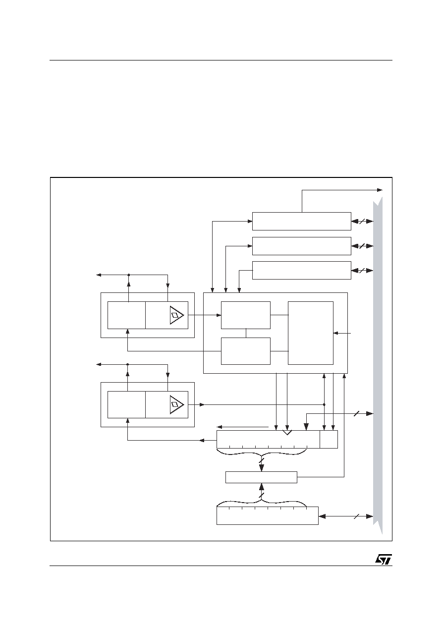
uPSD34xx - I
2
C INTERFACE
102/264
Serial I/O Engine (SIOE)
At the heart of the I
2
C interface is the hardware
SIOE, shown in Figure
43
. The SIOE automatically
handles low-level I
2
C bus protocol (data shifting,
handshaking, arbitration, clock generation and
synchronization) and it is controlled and monitored
by five SFRs.
The five SFRs shown in Figure
43
are:
S1CON - Interface Control (
Table
54., page 103
)
S1STA - Interface Status (
Table
56., page 106
)
S1DAT - Data Shift Register (
Table
57., page 107
)
S1ADR - Device Address (
Table
58., page 107
)
S1SETUP - Sampling Rate (
Table
59., page 108
)
Figure 43. I
2
C Interface SIOE Block Diagram
Open-
Drain
Output
Input
Open-
Drain
Output
Input
Comparator
S1SETUP - Sample Rate
Control (START Condition)
S1STA - Interface Status
S1CON - Interface Control
ACK
Bit
SCL / P3.7
Timing and
Control
Clock
Generation
Arbitration
and Sync
Periph
Clock
(fOSC)
SDA / P3.6
8032 MCU Bus
INTR to 8032
S1DAT - Shift Register
Serial DATA IN
Serial DATA OUT
Shift Direction
8
8
8
8
8
7
7
b0
b7
S1ADR - Device Address
b7
b0
AI09626

103/264
uPSD34xx - I
2
C INTERFACE
I
2
C Interface Control Register (S1CON)
Table 54. Serial Control Register S1CON (SFR DCh, Reset Value 00h)
Bit 7
Bit 6
Bit 5
Bit 4
Bit 3
Bit 2
Bit 1
Bit 0
CR2
ENI1
STA
STO
ADDR
AA
CR[1:0]
Details
Bit
Symbol
R/W
Function
7
CR2
R,W
This bit, along with bits CR1 and CR0, determine the SCL clock
frequency (f
SCL
) when SIOE is in Master mode. These bits create a clock
divisor for f
OSC
. See Table
55
.
6
ENI1
R,W
I
2
C Interface Enable
0 = SIOE disabled, 1 = SIOE enabled. When disabled, both SDA and
SCL signals are in high impedance state.
5
STA
R,W
START flag.
When set, Master mode is entered and SIOE generates a START
condition only if the I
2
C bus is not busy. When a START condition is
detected on the bus, the STA flag is cleared by hardware. When the STA
bit is set during an interrupt service, the START condition will be
generated after the interrupt service.
4
STO
R,W
STOP flag
When STO is set in Master mode, the SIOE generates a STOP condition.
When a STOP condition is detected, the STO flag is cleared by
hardware. When the STO bit is set during an interrupt service, the STOP
condition will be generated after the interrupt service.
3
ADDR
R,W
This bit is set when an address byte received in Slave mode matches the
device address programmed into the S1ADR register. The ADDR bit
must be cleared with firmware.
2
AA
R,W
Assert Acknowledge enable
If AA = 1, an acknowledge signal (low on SDA) is automatically returned
during the acknowledge bit-time on the SCL line when any of the
following three events occur:
1.
SIOE in Slave mode receives an address that matches contents of
S1ADR register
2.
A data byte has been received while SIOE is in Master Receiver
mode
3.
A data byte has been received while SIOE is a selected Slave
Receiver
When AA = 0, no acknowledge is returned (high on SDA during acknowl-
edge bit-time).
1, 0
CR1, CR0
R,W
These bits, along with bit CR2, determine the SCL clock frequency (f
SCL
)
when SIOE is in Master mode. These bits create a clock divisor for f
OSC
.
See Table
55
for values.
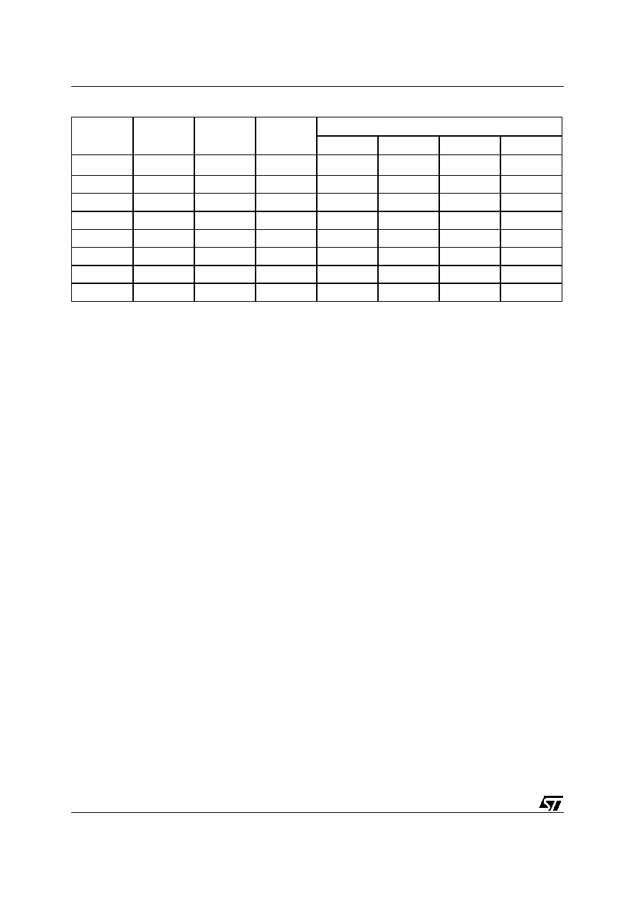
uPSD34xx - I
2
C INTERFACE
104/264
Table 55. Selection of the SCL Frequency in Master Mode based on f
OSC
Examples
Note: 1. These values are beyond the bit rate supported by uPSD34xx.
CR2
CR1
CR0
f
OSC
Divided by:
Bit Rate (kHz) @ f
OSC
12MHz f
OSC
24MHz f
OSC
36MHz f
OSC
40MHz f
OSC
0
0
0
32
375
750
X
(1)
X
(1)
0
0
1
48
250
500
750
833
0
1
0
60
200
400
600
666
0
1
1
120
100
200
300
333
1
0
0
240
50
100
150
166
1
0
1
480
25
50
75
83
1
1
0
960
12.5
25
37.5
41
1
1
1
1920
6.25
12.5
18.75
20

105/264
uPSD34xx - I
2
C INTERFACE
I
2
C Interface Status Register (S1STA)
The S1STA register provides status regarding im-
mediate activity and the current state of operation
on the I
2
C bus. All bits in this register are read-only
except bit 5, INTR, which is the interrupt flag.
Interrupt Conditions. If the I
2
C interrupt is en-
abled (EI
2
C = 1 in SFR named IEA, and EA =1 in
SFR named IE), and the SIOE is initialized, then
an interrupt is automatically generated when any
one of the following five events occur:
≠
When the SIOE receives an address that
matches the contents of the SFR, S1ADR.
Requirements: SIOE is in Slave Mode, and bit
AA = 1 in the SFR S1CON.
≠
When the SIOE receives General Call
address. Requirments: SIOE is in Slave Mode,
bit AA = 1 in the SFR S1CON
≠
When a complete data byte has been received
or transmitted by the SIOE while in Master
mode. The interrupt will occur even if the
Master looses arbitration.
≠
When a complete data byte has been received
or transmitted by the SIOE while in selected
Slave mode.
≠
A STOP condition on the bus has been
recognized by the SIOE while in selected
Slave mode.
Selected Slave mode means the device address
sent by the Master device at the beginning of the
current data transfer matched the address stored
in the S1ADR register.
If the I
2
C interrupt is not enabled, the MCU may
poll the INTR flag in S1STA.

uPSD34xx - I
2
C INTERFACE
106/264
Table 56. S1STA: I
2
C Interface Status register (SFR DDh, reset value 00h)
Bit 7
Bit 6
Bit 5
Bit 4
Bit 3
Bit 2
Bit 1
Bit 0
GC
STOP
INTR
TX_MODE
BBUSY
BLOST
ACK_RESP
SLV
Details
Bit
Symbol
R/W
Function
7
GC
R
General Call flag
GC = 1 if the General Call address of 00h was received when SIOE is in
Slave mode, and GC is cleared by a START or STOP condition on the
bus. If the SIOE is in Master mode when GC = 1, the Bus Lost condition
exists, and BLOST = 1.
6
STOP
R
STOP flag
STOP = 1 while SIOE detects a STOP condition on the bus when in
Master or Slave mode.
5
INTR
R,W
Interrupt flag
INTR is set to 1 by any of the five I
2
C interrupt conditions listed above.
INTR must be cleared by firmware.
4
TX_MODE
R
Transmission Mode flag
TX_MODE = 1 whenever the SIOE is in Master-Transmitter or Slave-
Transmitter mode. TX_MODE = 0 when SIOE is in any receiver mode.
3
BBUSY
R
Bus Busy flag
BBUSY = 1 when the I
2
C bus is in use. BBUSY is set by the SIOE when
a START condition exists on the bus and BBUSY is cleared by a STOP
condition.
2
BLOST
R
Bus Lost flag
BLOST is set when the SIOE is in Master mode and it looses the
arbitration process to another Master device on the bus.
1
ACK_RESP
R
Not Acknowledge Response flag
While SIOE is in Transmitter mode:
≠
After SIOE sends a byte, ACK_RESP = 1 whenever the external I
2
C
device receives the byte, but that device does NOT assert an
ackowledge signal (external device asserted a high on SDA during
the acknowledge bit-time).
≠
After SIOE sends a byte, ACK_RESP = 0 whenever the external I
2
C
device receives the byte, and that device DOES assert an
ackowledge signal (external device drove a low on SDA during the
acknowledge bit-time)
Note: If SIOE is in Master-Transmitter mode, and ACK_RESP = 1 due to
a Slave-Transmitter not sending an Acknowledge, a STOP condition will
not automatically be generated by the SIOE. The STOP condition must
be generated with S1CON.STO = 1.
0
SLV
R
Slave Mode flag
SLV = 1 when the SIOE is in Slave mode. SLV = 0 when the SIOE is in
Master mode (default).
107/264
uPSD34xx - I
2
C INTERFACE
I
2
C Data Shift Register (S1DAT)
The S1ADR register (Table
57
) holds a byte of se-
rial data to be transmitted or it holds a serial byte
that has just been received. The MCU may access
S1DAT while the SIOE is not in the process of
shifting a byte (the INTR flag indicates shifting is
complete).
While transmitting, bytes are shifted out MSB first,
and when receiving, bytes are shifted in MSB first,
through the Acknowledge Bit register as shown in
Figure 43., page 102
.
Bus Wait Condition. After the SIOE finishes re-
ceiving a byte in Receive mode, or transmitting a
byte in Transmit mode, the INTR flag (in S1STA)
is set and automatically a wait condition is im-
posed on the I
2
C bus (SCL held low by SIOE). In
Transmit mode, this wait condition is released as
soon as the MCU writes any byte to S1DAT. In Re-
ceive mode, the wait condition is released as soon
as the MCU reads the S1DAT register.
This method allows the user to handle transmit
and receive operations within an interrupt service
routine. The SIOE will automatically stall the I
2
C
bus at the appropriate time, giving the MCU time
to get the next byte ready to transmit or time to
read the byte that was just received.
Table 57. S1DAT: I
2
C Data Shift register (SFR DEh, reset value 00h)
I
2
C Address Register (S1ADR)
The S1ADR register (Table
58
) holds the 7-bit de-
vice address used when the SIOE is operating as
a Slave. When the SIOE receives an address from
a Master, it will compare this address to the con-
tents of S1ADR, as shown in
Figure
43., page 102
.
If the 7 bits match, the INTR Interrupt flag (in
S1STA) is set, and the ADDR Bit (in S1CON) is
set. The SIOE cannot modify the contents S1ADR,
and S1ADR is not used during Master mode.
Table 58. S1ADR: I
2
C Address register (SFR DFh, reset value 00h)
Bit 7
Bit 6
Bit 5
Bit 4
Bit 3
Bit 2
Bit 1
Bit 0
S1DAT[7:0]
Details
Bit
Symbol
R/W
Function
7:0
S1DAT[7:0]
R/W
Holds the data byte to be transmitted in Transmit mode, or it holds the
data byte received in Receiver mode.
Bit 7
Bit 6
Bit 5
Bit 4
Bit 3
Bit 2
Bit 1
Bit 0
SLA6
SLA5
SLA4
SLA3
SLA2
SLA1
SLA0
≠
Details
Bit
Symbol
R/W
Function
7:1
SLA[6:0]
R/W
Stores desired 7-bit device address, used when SIOE is in Slave mode.
0
≠
≠
Not used

uPSD34xx - I
2
C INTERFACE
108/264
I
2
C START Sample Setting (S1SETUP)
The S1SETUP register (Table
59
) determines how
many times an I
2
C bus START condition will be
sampled before the SIOE validates the START
condition, giving the SIOE the ability to reject noise
or illegal transmissions.
Because the minimum duration of an START con-
dition varies with I
2
C bus speed (f
SCL
), and also
because the uPSD34xx may be operated with a
wide variety of frequencies (f
OSC
), it is necessary
to scale the number of samples per START condi-
tion based on f
OSC
and f
SCL
.
In Slave mode, the SIOE recognizes the beginning
of a START condition when it detects a '1'-to-'0'
transition on the SDA bus line while the SCL line is
high (see
Figure 42., page 100
). The SIOE must
then validate the START condition by sampling the
bus lines to ensure SDA remains low and SCL re-
mains high for a minimum amount of hold time,
t
HLDSTA
. Once validated, the SIOE begins receiv-
ing the address byte that follows the START con-
dition.
If the EN_SS Bit (in the S1SETUP Register) is not
set, then the SIOE will sample only once after de-
tecting the '1'-to-'0' transition on SDA. This single
sample is taken 1/f
OSC
seconds after the initial 1-
to-0 transition was detected. However, more sam-
ples should be taken to ensure there is a valid
START condition.
To take more samples, the SIOE should be initial-
ized such that the EN_SS Bit is set, and a value is
written to the SMPL_SET[6:0] field of the
S1SETUP Register to specify how many samples
to take. The goal is to take a good number of sam-
ples during the minimum START condition hold
time, t
HLDSTA
, but no so many samples that the
bus will be sampled after t
HLDSTA
expires.
Table 60., page 109
describes the relationship be-
tween the contents of S1SETUP and the resulting
number of I
2
C bus samples that SIOE will take af-
ter detecting the 1-to-0 transition on SDA of a
START condition.
Important: Keep in mind that the time between
samples is always 1/f
OSC
.
The minimum START condition hold time, t
HLDS-
TA
, is different for the three common I
2
C speed
categories per
Table 61., page 109
.
Table 59. S1SETUP: I
2
C START Condition Sample Setup register (SFR DBh, reset value 00h)
Note: 1. Sampling SCL and SDA lines begins after '1'-to-'0' transition on SDA occurred while SCL is high. Time between samples is 1/f
OSC
.
Bit 7
Bit 6
Bit 5
Bit 4
Bit 3
Bit 2
Bit 1
Bit 0
EN_SS
SMPL_SET[6:0]
Details
Bit
Symbol
R/W
Function
7
EN_SS
R/W
Enable Sample Setup
EN_SS = 1 will force the SIOE to sample
(1)
a START condition on the bus
the number of times specified in SMPL_SET[6:0].
EN_SS = 0 means the SIOE will sample
(1)
a START condition only one
time, regardless of the contents of SMPL_SET[6:0].
6:0
SMPL_SET
[6:0]
≠
Sample Setting
Specifies the number of bus samples
(1)
taken during a START condition.
See Table
60
for values.

109/264
uPSD34xx - I
2
C INTERFACE
Table 60. Number of I
2
C Bus Samples Taken after 1-to-0 Transition on SDA (START Condition)
Table 61. Start Condition Hold Time
Note: 1. 833KHz is maximum for uPSD34xx devices.
Contents of S1SETUP
Resulting value for S1SETUP
Resulting Number of Samples
Taken After 1-to-0 on SDA Line
SS_EN bit
SMPL_SET[6:0]
0
XXXXXXXb
00h (default)
1
1
0000000b
80h
1
1
0000001b
81h
2
1
0000010b
82h
3
...
...
...
...
1
0001011b
8Bh
12
1
0010111b
97h
24
...
...
...
...
1
1111111b
FFh
128
I
2
C Bus Speed
Range of I
2
C Clock Speed (f
SCL
)
Minimum START Condition Hold
Time (
t
HLDSTA
)
Standard
Up to 100KHz
4000ns
Fast
101KHz to
400KHz
600ns
High
401KHz to 833KHz
(1)
160ns
uPSD34xx - I
2
C INTERFACE
110/264
Table
62
provides recommended settings for
S1SETUP based on various combinations of f
OSC
and f
SCL
. Note that the "Total Sample Period"
times in
Table 61., page 109
are typically slightly
less than the minimum START condition hold time,
t
HLDSTA
for a given I
2
C bus speed.
Important: The SCL bit rate f
SCL
must first be de-
termined by bits CR[2:0] in the SFR S1CON be-
fore a value is chosen for SMPL_SET[6:0] in the
SFR S1SETUP.
Table 62. S1SETUP Examples for Various I
2
C Bus Speeds and Oscillator Frequencies
Note: 1. Not compatible with High Speed I
2
C.
I
2
C Bus
Speed,
f
SCL
Parameter
Oscillator Frequency, f
OSC
6 MHz
12 MHz
24 MHz
33 MHz
40 MHz
Standard
Recommended
S1SETUP Value
93h
A7h
CFh
EEh
FFh
Number of Samples
20
40
80
111
128
Time Between Samples
166.6ns
83.3ns
41.6ns
30ns
25ns
Total Sampled Period
3332ns
3332ns
3332ns
3333ns
3200ns
Fast
Recommended
S1SETUP Value
82h
85h
8Bh
90h
93h
Number of Samples
3
6
12
17
20
Time Between Samples
166.6ns
83.3ns
41.6ns
30ns
25ns
Total Sampled Period
500ns
500ns
500ns
510ns
500ns
High
Recommended
S1SETUP Value
(Note 1)
80
82
83
84
Number of Samples
-
1
3
4
5
Time Between Samples
-
83.3ns
41.6ns
30ns
25ns
Total Sampled Period
-
83.3
125ns
120ns
125ns

111/264
uPSD34xx - I
2
C INTERFACE
I
2
C Operating Sequences
The following pseudo-code explains hardware
control for these I
2
C functions on the uPSD34xx:
≠
Initialize the Interface
≠
Function as Master-Transmitter
≠
Function as Master-Receiver
≠
Function as Slave-Transmitter
≠
Function as Slave-Receiver
≠
Interrupt Service Routine
Full C code drivers for the uPSD34xx I
2
C inter-
face, and other interfaces are available from the
web at www.st.com\psm.
Initialization after a uPSD34xx reset
Ensure pins P3.6 and P3.7 are GPIO in-
puts
≠
SFR P3.7 = 1 and SFR P3.6 = 1
Configure pins P3.6 and P3.7 as I
2
C
≠
SFR P3SFS.6 = 1 and P3SFS.7 = 1
Set I
2
C clock prescaler to determine
f
SCL
≠
SFR S1CON.CR[2:0] = desired SCL
freq.
Set bus START condition sampling
≠
SFR S1SETUP[7:0] = number of sam-
ples
Enable individual I
2
C interrupt and
set priority
≠
SFR IEA.I2C = 1
≠
SFR IPA.I2C = 1 if high priority is
desired
Set the Device address for Slave mode
≠
SFR S1ADR = XXh, desired address
Enable SIOE (as Slave) to return an
ACK signal
≠
SFR S1CON.AA = 1
Master-Transmitter
Disable all interrupts
≠
SFR IE.EA = 0
Set pointer to global data xmit buff-
er, set count
≠
*xmit_buf = *pointer to data
≠
buf_length = number of bytes to
xmit
Set global variables to indicate Mas-
ter-Xmitter
≠
I2C_master = 1, I2C_xmitter = 1
Disable Master from returning an ACK
≠
SFR S1CON.AA = 0
Enable I2C SIOE
≠
SFR S1CON.INI1 = 1
Transmit Address and R/W bit = 0 to
Slave
≠
Is bus not busy? (SFR S1STA.BBUSY
= 0?)
<If busy, then test until not busy>
≠
SFR S1DAT[7:0] = Load Slave Ad-
dress & FEh
≠
SFR S1CON.STA = 1, send START on
bus
<bus transmission begins>
Enable All Interrupts and go do some-
thing else
≠
SFR IE.EA = 1
Master-Receiver
Disable all interrupts
≠
SFR IE.EA = 0
Set pointer to global data recv buff-
er, set count
≠
*recv_buf = *pointer to data
≠
buf_length = number of bytes to
recv
Set global variables to indicate Mas-
ter-Xmitter
≠
I2C_master = 1, I2C_xmitter = 0
Disable Master from returning an ACK
≠
SFR S1CON.AA = 0
Enable I2C SIOE
≠
SFR S1CON.INI1 = 1
Transmit Address and R/W bit = 1 to
Slave
≠
Is bus not busy? (SFR S1STA.BBUSY
= 0?)
<If busy, then test until not busy>
≠
SFR S1DAT[7:0] = Load Slave Ad-
dress # 01h
≠
SFR S1CON.STA = 1, send START on
bus
<bus transmission begins>
Enable All Interrupts and go do some-
thing else
≠
SFR IE.EA = 1

uPSD34xx - I
2
C INTERFACE
112/264
Slave-Transmitter
Disable all interrupts
≠
SFR IE.EA = 0
Set pointer to global data xmit buff-
er, set count
≠
*xmit_buf = *pointer to data
≠
buf_length = number of bytes to
xmit
Set global variables to indicate Mas-
ter-Xmitter
≠
I2C_master = 0, I2C_xmitter = 1
Enable SIOE
≠
SFR S1CON.INI1 = 1
Prepare to Xmit first data byte
≠
SFR S1DAT[7:0] = xmit_buf[0]
Enable All Interrupts and go do some-
thing else
≠
SFR IE.EA = 1
Slave-Receiver
Disable all interrupts
≠
SFR IE.EA = 0
Set pointer to global data recv buff-
er, set count
≠
*recv_buf = *pointer to data
≠
buf_length = number of bytes to
recv
Set global variables to indicate Mas-
ter-Xmitter
≠
I2C_master = 0, I2C_xmitter = 0
Enable SIOE
≠
SFR S1CON.INI1 = 1
Enable All Interrupts and go do some-
thing else
≠
SFR IE.EA = 1
Interrupt Service Routine (ISR). A typical I
2
C
interrupt service routine would handle a interrupt
for any of the four combinations of Master/Slave
and Transmitter/Receiver. In the example routines
above, the firmware sets global variables,
I2C_master and I2C_xmitter, before enabling in-
terrupts. These flags tell the ISR which one of the
four cases to process. Following is pseudo-code
for high-level steps in the I
2
C ISR:
Begin I
2
C ISR <I
2
C interrupt just occurred>:
Clear I2C interrupt flag:
≠
S1STA.INTR = 0
Read status of SIOE, put in to vari-
able, status
≠
status = S1STA
Read global variables that determine
the mode
≠
mode
<=
(I2C_master, I2C_slave)
If mode is Master-Transmitter
Bus Arbitration lost? (sta-
tus.BLOST=1?)
If Yes, Arbitration was lost:
≠
S1DAT = dummy, write to release bus
≠
Exit ISR, SIOE will switch to Slave
Recv mode
If No, Arbitration was not
lost, continue:
ACK recvd from Slave? (sta-
tus.ACK_RESP=0?)
If No, an ACK was not received:
≠
S1CON.STO = 1, set STOP bus condi-
tion
≠
<STOP occurs after ISR exit>
≠
S1DAT = dummy, write to release bus
≠
Exit ISR
If Yes, ACK was received, then
continue:
≠
S1DAT = xmit_buf[buffer_index],
transmit byte
Was that the last byte of data to
transmit?
If No, it was not the last byte,
then:
≠
Exit ISR, transmit next byte on
next interrupt
If Yes, it was the last byte,
then:
≠
S1CON.STO = 1, set STOP bus condi-
tion
<STOP occurs after ISR exit>
≠
S1DAT = dummy, write to release bus
≠
Exit ISR

113/264
uPSD34xx - I
2
C INTERFACE
Else If mode is Master-Receiver:
Bus Arbitration lost? (sta-
tus.BLOST=1?)
If Yes, Arbitration was lost:
≠
S1DAT = dummy, write to release bus
≠
Exit ISR, SIOE will switch to Slave
Recv mode
If No, Aribitration was not
lost, continue:
Is this Interrupt from sending an ad-
dress to Slave, or is it from receiv-
ing a data byte from Slave?
If its from sending Slave ad-
dress, goto A:
If its from receiving Slave da-
ta, goto B:
A:
(Interrupt is from Master sending
addr to Slave)
ACK recvd from Slave? (sta-
tus.ACK_RESP=0?)
If No, an ACK was not received:
≠
S1CON.STO = 1, set STOP condition
<STOP occurs after ISR exit>
≠
dummy = S1DAT, read to release bus
≠
Exit ISR
If Yes, ACK was received, then
continue:
≠
dummy = S1DAT, read to release bus
Does Master want to receive just one
data byte?
If Yes, do not allow Master to
ACK on next interrupt:
<S1CON.AA is already 0>
≠
Exit ISR, now ready to recv one
byte from Slv
If No, Master can ACK next byte
from Slv
≠
S1CON.AA = 1, allow Master to send
ACK
≠
Exit ISR, now ready to recv data
from Slave
B:
(Interrupt is from Master recving
data from Slv)
≠
recv_buf[buffer_index] = S1DAT,
read byte
Is this the last data byte to receive
from Slave?
If Yes, tell Slave to stop
transmitting:
≠
S1CON.STO = 1, set STOP bus condi-
tion
<STOP occurs after ISR exit>
≠
Exit ISR, finished receiving data
from Slave
If No, continue:
Is this the next to last byte to re-
ceive from Slave?
If this is the next to last
byte, do not allow Master to ACK
on next interrupt.
≠
S1CON.AA = 0, don't let Master re-
turn ACK
≠
Exit ISR, now ready to recv last
byte from Slv
If this is not next to last
byte, let Master send ACK to
Slave
<S1CON.AA is already 1>
≠
Exit ISR, ready to recv more bytes
from Slave
Else If mode is Slave-Transmitter:
Is this Intr from SIOE detecting a
STOP on bus?
If Yes, a STOP was detected:
≠
S1DAT = dummy, write to release bus
≠
Exit ISR, Master needs no more data
bytes
If No, a STOP was not detected,
continue:
ACK recvd from Master? (sta-
tus.ACK_RESP=0?)
If No, an ACK was not received:
≠
S1DAT = dummy, write to release bus
≠
Exit ISR, Master needs no more data
bytes
If Yes, ACK was received, then
continue:
≠
S1DAT = xmit_buf[buffer_index],
transmit byte
≠
Exit ISR, transmit next byte on
next interrupt

uPSD34xx - I
2
C INTERFACE
114/264
Else If mode is Slave-Receiver:
Is this Intr from SIOE detecting a
STOP on bus?
If Yes, a STOP was detected:
≠
recv_buf[buffer_index] = S1DAT,
get last byte
≠
Exit ISR, Master has sent last byte
If No, a STOP was not detected,
continue:
Determine if this Interrupt is from
receiving an address or a data byte
from a Master.
Is (S1CON.ADDR = 1 and S1CON.AA =1)?
If No, intr is from receiving
data, goto C:
If Yes, intr is from an address,
continue:
≠
slave_is_adressed = 1, local vari-
able set true
<indicates Master selected this
slave>
≠
S1CON.ADDR = 0, clear address
match flag
Determine if R/W bit indicates trans-
mit or receive.
Does status.TX_MODE = 1?
If Yes, Master wants transmit
mode
≠
Exit ISR, indicate Master wants
Slv-Xmit mode
If No, Master wants Slave-Recv
mode
≠
dummy = S1DAT, read to release bus
≠
Exit ISR, ready to recv data on
next interrupt
C:
(Interrupt is from Slv receiving
data from Mastr)
≠
recv_buf[buffer_index] = S1DAT,
read byte
≠
Exit ISR, recv next byte on next
interrupt
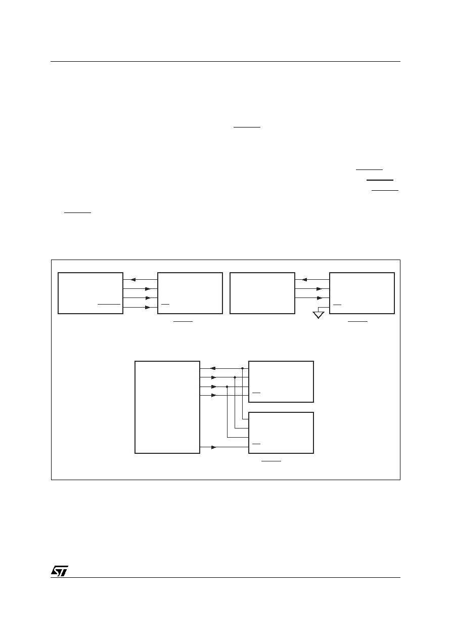
115/264
uPSD34xx - SPI (SYNCHRONOUS PERIPHERAL INTERFACE)
SPI (SYNCHRONOUS PERIPHERAL INTERFACE)
uPSD34xx devices support one serial SPI inter-
face in Master Mode only. This is a three- or four-
wire synchronous communication channel, capa-
ble of full-duplex operation on 8-bit serial data
transfers. The four SPI bus signals are:
SPIRxD
Pin P1.5 or P4.5 receives data from the Slave
SPI device to the uPSD34xx
SPITxD
Pin P1.6 or P4.6 transmits data from the
uPSD34xx to the Slave SPI device
SPICLK
Pin P1.4 or P4.4 clock is generated from the
uPSD34xx to the SPI Slave device
SPISEL
Pin P1.7 or P4.7 selects the signal from the
uPSD34xx to an individual Slave SPI device
This SPI interface supports single-Master/multi-
ple-Slave connections. Multiple-Master connec-
tions are not directly supported by the uPSD34xx
(no internal logic for collision detection).
If more than one Slave device is required, the
SPISEL signal may be generated from uPSD34xx
GPIO outputs (one for each Slave) or from the
PLD outputs of the PSD Module.
Figure 44.
illus-
trates three examples of SPI device connections
using the uPSD34xx:
Single-Master/Single-Slave with SPISEL
Single-Master/Single-Slave without SPISEL
Single-Master/Multiple-Slave without SPISEL
Figure 44. SPI Device Connection Examples
SPI Bus
SPI Bus
SPI Bus
SPITxD
SPIRxD
uPSD34xx
SPI Master
SPI Slave
Device
SPICLK
SPISEL
AI07853b
MOSI
MISO
SCLK
Single-Master/Single-Slave, with SPISEL
Single-Master/Single-Slave, without SPISEL
Single-Master/Multiple-Slave, without SPISEL
SS
SPI Slave
Device
MOSI
MISO
SCLK
SS
SPI Slave
Device
MOSI
MISO
SCLK
SS
SS
SPITxD
SPIRxD
uPSD34xx
SPI Master
SPI Slave
Device
SPICLK
SPITxD
SPIRxD
uPSD34xx
SPI Master
SPICLK
GPIO or PLD
GPIO or PLD
MOSI
MISO
SCLK
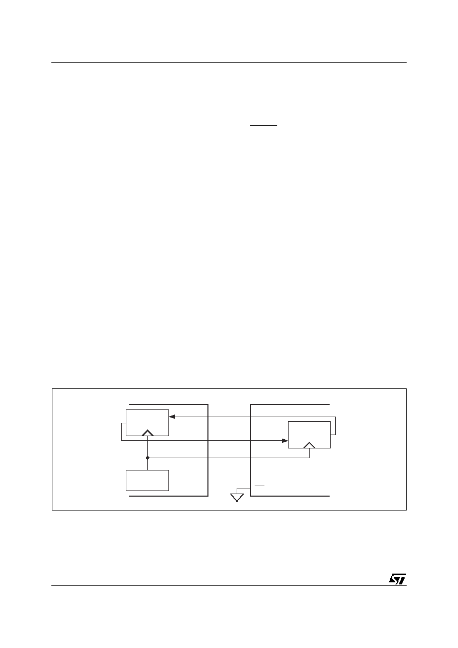
uPSD34xx - SPI (SYNCHRONOUS PERIPHERAL INTERFACE)
116/264
SPI Bus Features and Communication Flow
The SPICLK signal is a gated clock generated
from the uPSD34xx (Master) and regulates the
flow of data bits. The Master may transmit at a va-
riety of baud rates, and the SPICLK signal will
clock one period for each bit of transmitted data.
Data is shifted on one edge of SPICLK and sam-
pled on the opposite edge.
The SPITxD signal is generated by the Master and
received by the Slave device. The SPIRxD signal
is generated by the Slave device and received by
the Master. There may be no more than one Slave
device transmitting data on SPIRxD at any given
time in a multi-Slave configuration. Slave selection
is accomplished when a Slave's "Slave Select"
(SS) input is permanently grounded or asserted
active-low by a Master device. Slave devices that
are not selected do not interfere with SPI activities.
Slave devices ignore SPICLK and keep their
MISO output pins in high-impedance state when
not selected.
The SPI specification allows a selection of clock
polarity and clock phase with respect to data. The
uPSD34xx supports the choice of clock polarity,
but it does not support the choice of clock phase
(phase is fixed at what is typically known as
CPHA = 1). See
Figure 46.
and
Figure
47., page 117
for SPI data and clock relationships.
Referring to these figures (
46
and
47
), when the
phase mode is defined as such (fixed at
CPHA =1), in a new SPI data frame, the Master
device begins driving the first data bit on SPITxD
at the very first edge of the first clock period of SPI-
CLK.
The Slave device will use this first clock edge as a
transmission start indicator, and therefore the
Slave's Slave Select input signal may remain
grounded in a single-Master/single-Slave configu-
ration (which means the user does not have to use
the SPISEL signal from uPSD34xx in this case).
The SPI specification does not specify high-level
protocol for data exchange, only low-level bit-seri-
al transfers are defined.
Full-Duplex Operation
When an SPI transfer occurs, 8 bits of data are
shifted out on one pin while a different 8 bits of
data are simultaneously shifted in on a second pin.
Another way to view this transfer is that an 8-bit
shift register in the Master and another 8-bit shift
register in the Slave are connected as a circular
16-bit shift register. When a transfer occurs, this
distributed shift register is shifted 8 bit positions;
thus, the data in the Master and Slave devices are
effectively exchanged (see
Figure 45.
).
Bus-Level Activity
Figure 46.
details an SPI receive operation (with
respect to bus Master) and
Figure 47.
details an
SPI transmit operation. Also shown are internal
flags available to firmware to manage data flow.
These flags are accessed through a number of
SFRs.
Note: The uPSD34xx SPI interface SFRs allow
the choice of transmitting the most significant bit
(MSB) of a byte first, or the least significant bit
(LSB) first. The same bit-order applies to data re-
ception. Figures
46
and
47
illustrate shifting the
LSB first.
Figure 45. SPI Full-Duplex Data Exchange
SPI Bus
Slave Device
Master Device
AI10485
SS
SPITxD
SPIRxD
Baud Rate
Generator
8-Bit Shift
Register
8-Bit Shift
Register
SPICLK
MOSI
MISO
SCLK
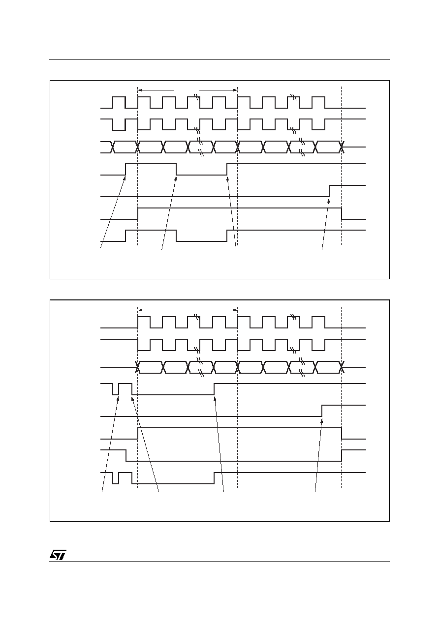
117/264
uPSD34xx - SPI (SYNCHRONOUS PERIPHERAL INTERFACE)
Figure 46. SPI Receive Operation Example
Figure 47. SPI Transmit Operation Example
Bit7
SPICLK
(SPO=0)
SPICLK
(SPO=1)
SPIRXD
Bit0
Bit1
Bit7
Bit0
Bit1
Bit7
1 frame
RISF
RORIS
BUSY
SPIINTR
SPIRDR Full
interrupt requested
Interrupt handler
read data in SPIRDR
SPIRDR Full
interrupt requested
Transmit End
interrupt requested
AI07855
Bit0
SPICLK
(SPO=0)
SPICLK
(SPO=1)
SPITXD
Bit1
Bit7
Bit0
Bit1
Bit7
1 frame
TISF
TEISF
BUSY
SPIINTR
SPITDR Empty
interrupt requested
Interrupt handler
write data in TDR
SPITDR Empty
interrupt requested
Transmit End
interrupt requested
SPISEL
AI07854
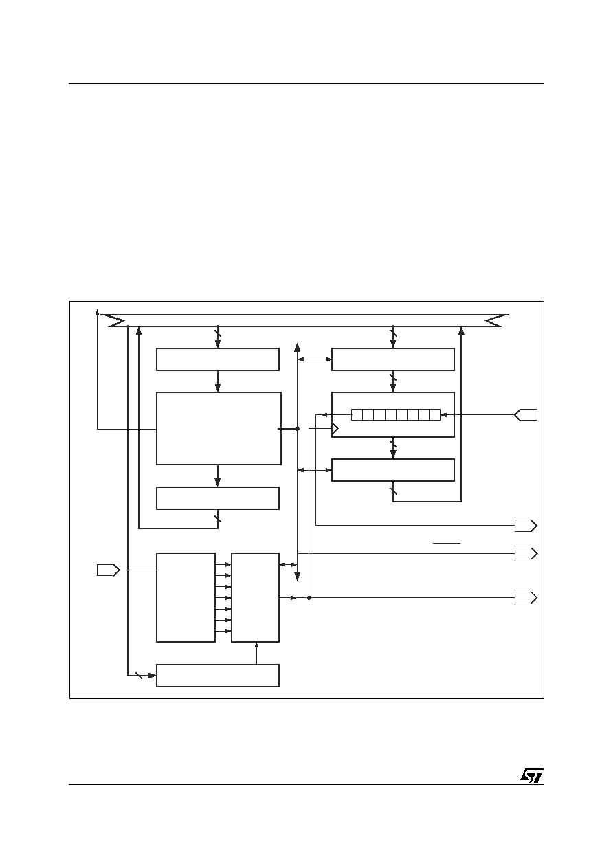
uPSD34xx - SPI (SYNCHRONOUS PERIPHERAL INTERFACE)
118/264
SPI SFR Registers
Six SFR registers control the SPI interface:
SPICON0 (
Table 63., page 120
) for interface
control
SPICON1 (
Table 64., page 121
) for interrupt
control
SPITDR (SFR D4h, Write only) holds byte to
transmit
SPIRDR (SFR D5h, Read only) holds byte
received
SPICLKD (
Table 65., page 121
) for clock
divider
SPISTAT (
Table 66., page 122
) holds
interface status
The SPI interface functional block diagram (
Figure
48.
) shows these six SFRs. Both the transmit and
receive data paths are double-buffered, meaning
that continuous transmitting or receiving (back-to-
back transfer) is possible by reading from SPIRDR
or writing data to SPITDR while shifting is taking
place. There are a number of flags in the SPISTAT
register that indicate when it is full or empty to as-
sist the 8032 MCU in data flow management.
When enabled, these status flags will cause an in-
terrupt to the MCU.
Figure 48. SPI Interface, Master Mode Only
SPITDR - TRANSMIT REGISTER
SPITxD / P1.6 or P4.6
TIMING AND CONTROL
(fOSC)
INTR
to
8032
SPIRDR - RECEIVE REGISTER
8-bit SHIFT REGISTER
8
8
8
8
SPIRxD /
P1.5 or P4.5
SPICON0, SPICON1
- CONTROL REGISTERS
8
SPISTAT - STATUS REGISTER
8
8032 MCU DATA BUS
CLOCK
GENERATE
SPISEL / P1.7 or P4.7
SPICLK / P1.4 or P4.4
CLOCK
DIVIDE
˜1
˜4
˜8
˜16
˜32
˜64
˜128
SPICLKD - DIVIDE SELECT
8
PERIPH_CLK
AI10486

119/264
uPSD34xx - SPI (SYNCHRONOUS PERIPHERAL INTERFACE)
SPI Configuration
The SPI interface is reset by the MCU reset, and
firmware needs to initialize the SFRs SPICON0,
SPICON1, and SPICLKD to define several opera-
tion parameters.
The SPO Bit in SPICON0 determines the clock po-
larity. When SPO is set to '0,' a data bit is transmit-
ted on SPITxD from one rising edge of SPICLK to
the next and is guaranteed to be valid during the
falling edge of SPICLK. When SPO is set to '1,' a
data bit is transmitted on SPITxD from one falling
edge of SPICLK to the next and is guaranteed to
be valid during the rising edge of SPICLK. The
uPSD34xx will sample received data on the appro-
priate edge of SPICLK as determined by SPO.
The effect of the SPO Bit can be seen in
Figure 46.
and
Figure 47., page 117
.
The FLSB Bit in SPICON0 determines the bit order
while transmitting and receiving the 8-bit data.
When FLSB is '0,' the 8-bit data is transferred in or-
der from MSB (first) to LSB (last). When FLSB Bit
is set to '1,' the data is transferred in order from
LSB (first) to MSB (last).
The clock signal generated on SPICLK is derived
from the internal PERIPH_CLK signal.
PERIPH_CLK always operates at the frequency,
f
OSC
, and runs constantly except when stopped in
MCU Power Down mode. SPICLK is a result of di-
viding PERIPH_CLK by a sum of different divisors
selected by the value contained in the SPICLKD
register. The default value in SPICLKD after a re-
set divides PERIPH_CLK by a factor of 4. The bits
in SPICLKD can be set to provide resulting divisor
values in of sums of multiples of 4, such as 4, 8,
12, 16, 20, all the way up to 252. For example, if
SPICLKD contains 0x24, SPICLK has the fre-
quency of PERIH_CLK divided by 36 decimal.
The SPICLK frequency must be set low enough to
allow the MCU time to read received data bytes
without loosing data. This is dependent upon
many things, including the crystal frequency of the
MCU and the efficiency of the SPI firmware.
Dynamic Control
At runtime, bits in registers SPICON0, SPICON1,
and SPISTAT are managed by firmware for dy-
namic control over the SPI interface. The bits
Transmitter Enable (TE) and Receiver Enable
(RE) when set will allow transmitting and receiving
respectively. If TE is disabled, both transmitting
and receiving are disabled because SPICLK is
driven to constant output logic `0' (when SPO = 0)
or logic '1' (when SPO = 1).
When the SSEL Bit is set, the SPISEL pin will drive
to logic '0' (active) to select a connected slave de-
vice at the appropriate time before the first data bit
of a byte is transmitted, and SPISEL will automat-
ically return to logic '1' (inactive) after transmitting
the eight bit of data, as shown in
Figure
47., page 117
. SPISEL will continue to automati-
cally toggle this way for each byte data transmis-
sion while the SSEL bit is set by firmware. When
the SSEL Bit is cleared, the SPISEL pin will drive
to constant logic '1' and stay that way (after a
transmission in progress completes).
The Interrupt Enable Bits (TEIE, RORIE,TIE, and
RIE) when set, will allow an SPI interrupt to be
generated to the MCU upon the occurrence of the
condition enabled by these bits. Firmware must
read the four corresponding flags in the SPISTAT
register to determine the specific cause of inter-
rupt. These flags are automatically cleared when
firmware reads the SPISTAT register.
uPSD34xx - SPI (SYNCHRONOUS PERIPHERAL INTERFACE)
120/264
Table 63. SPICON0: Control Register 0 (SFR D6h, Reset Value 00h)
Bit 7
Bit 6
Bit 5
Bit 4
Bit 3
Bit 2
Bit 1
Bit 0
≠
TE
RE
SPIEN
SSEL
FLSB
SBO
≠
Details
Bit
Symbol
R/W
Definition
7
≠
≠
Reserved
6
TE
RW
Transmitter Enable
0 = Transmitter is disabled
1 = Transmitter is enabled
5
RE
RW
Receiver Enable
0 = Receiver is disabled
1 = Receiver is enabled
4
SPIEN
RW
SPI Enable
0 = Entire SPI Interface is disabled
1 = Entire SPI Interface is enabled
3
SSEL
RW
Slave Selection
0 = SPISEL output pin is constant logic '1' (slave device not selected)
1 = SPISEL output pin is logic '0' (slave device is selected) during data
transfers
2
FLSB
RW
First LSB
0 = Transfer the most significant bit (MSB) first
1 = Transfer the least significant bit (LSB) first
1
SPO
≠
Sampling Polarity
0 = Sample transfer data at the falling edge of clock (SPICLK is '0' when
idle)
1 = Sample transfer data at the rising edge of clock (SPICLK is '1' when
idle)
0
≠
≠
Reserved
121/264
uPSD34xx - SPI (SYNCHRONOUS PERIPHERAL INTERFACE)
Table 64. SPICON1: SPI Interface Control Register 1 (SFR D7h, Reset Value 00h)
Table 65. SPICLKD: SPI Prescaler (Clock Divider) Register (SFR D2h, Reset Value 04h)
Bit 7
Bit 6
Bit 5
Bit 4
Bit 3
Bit 2
Bit 1
Bit 0
≠
≠
≠
≠
TEIE
RORIE
TIE
RIE
Details
Bit
Symbol
R/W
Definition
7-4
≠
≠
Reserved
3
TEIE
RW
Transmission End Interrupt Enable
0 = Disable Interrupt for Transmission End
1 = Enable Interrupt for Transmission End
2
RORIE
RW
Receive Overrun Interrupt Enable
0 = Disable Interrupt for Receive Overrun
1 = Enable Interrupt for Receive Overrun
1
TIE
RW
Transmission Interrupt Enable
0 = Disable Interrupt for SPITDR empty
1 = Enable Interrupt for SPITDR empty
0
RIE
RW
Reception Interrupt Enable
0 = Disable Interrupt for SPIRDR full
1 = Enable Interrupt for SPIRDR full
Bit 7
Bit 6
Bit 5
Bit 4
Bit 3
Bit 2
Bit 1
Bit 0
DIV128
DIV64
DIV32
DIV16
DIV8
DIV4
≠
≠
Details
Bit
Symbol
R/W
Definition
7
DIV128
RW
0 = No division
1 = Divide f
OSC
clock by 128
6
DIV64
RW
0 = No division
1 = Divide f
OSC
clock by 64
5
DIV32
RW
0 = No division
1 = Divide f
OSC
clock by 32
4
DIV16
RW
0 = No division
1 = Divide f
OSC
clock by 16
3
DIV8
RW
0 = No division
1 = Divide f
OSC
clock by 8
2
DIV4
RW
0 = No division
1 = Divide f
OSC
clock by 4
1-0
Not Used
≠
uPSD34xx - SPI (SYNCHRONOUS PERIPHERAL INTERFACE)
122/264
Table 66. SPISTAT: SPI Interface Status Register (SFR D3h, Reset Value 02h)
Bit 7
Bit 6
Bit 5
Bit 4
Bit 3
Bit 2
Bit 1
Bit 0
≠
≠
≠
BUSY
TEISF
RORISF
TISF
RISF
Details
Bit
Symbol
R/W
Definition
7-5
≠
≠
Reserved
4
BUSY
R
SPI Busy
0 = Transmit or Receive is completed
1 = Transmit or Receive is in process
3
TEISF
R
Transmission End Interrupt Source flag
0 = Automatically resets to '0' when firmware reads this register
1 = Automatically sets to '1' when transmission end occurs
2
RORISF
R
Receive Overrun Interrupt Source flag
0 = Automatically resets to '0' when firmware reads this register
1 = Automatically sets to '1' when receive overrun occurs
1
TISF
R
Transfer Interrupt Source flag
0 = Automatically resets to '0' when SPITDR is full (just after the SPITDR
is written)
1 = Automatically sets to '1' when SPITDR is empty (just after byte loads
from SPITDR into SPI shift register)
0
RISF
R
Receive Interrupt Source flag
0 = Automatically resets to '0' when SPIRDR is empty (after the SPIRDR
is read)
1 = Automatically sets to '1' when SPIRDR is full

123/264
uPSD34xx - USB INTERFACE
USB INTERFACE
uPSD34xx devices provide a full speed USB (Uni-
versal Serial Bus) device interface. The serial in-
terface engine (SIE) provides the interface
between the CPU and the USB (see
Figure 49.
).
Notes:
1. For a list of known limitations of USB interface
for uPSD34xx devices, please refer to
IMPOR-
TANT NOTES, page 262
.
2. Please make sure you have the latest 3400
USB firmware.
The USB module supports the following features:
USB 2.0 compliant to full-speed mode (12
Mbps)
3.3V USB transceiver
Five endpoints including Control endpoint 0
≠
Each endpoint includes two 64 byte
FIFOs, one for IN and one for OUT
transactions
≠
Endpoints 1 through 4 support Interrupt
and Bulk transfers
USB Bus Suspend detection and Resume
generation
PLL Multiplier to generate the 48 MHz as
required for USB support.
Interrupts for various USB bus conditions.
Performs NRZI encoding and decoding, bit
stuffing, CRC generation and checking, and
serial/parallel data conversion
Double buffering (using FIFO pairing) for
efficient data transfer in Bulk transfer
Busy bit-based FIFO status monitoring
FIFOs accessible via XDATA space
The analog front-end of the USB module is an on-
chip USB transceiver. It is designed to allow volt-
age levels equal to V
DD
from the standard logic to
interface with the physical layer of the USB. It is
capable of receiving and transmitting serial data at
full speed (12 Mb/s).
The SIE is the digital-front-end of the USB block.
This module recovers the 12MHz clock, detects
the USB sync word, and handles all low-level USB
protocols and error checking. The bit-clock recov-
ery circuit recovers the clock from the incoming
USB data stream and is able to track jitter and fre-
quency drift according to the USB specifications.
The SIE also translates the electrical USB signals
into bytes or signals. When there is a USB device
address match, the USB data is directed to an
endpoint's FIFO for OUT transactions and read
from an endpoint's FIFO for IN transactions. Con-
trol transfers are supported on Endpoint0 and in-
terrupt and bulk data transfers are supported on
Endpoints1 through 4. The device's USB address
and the enabling of the endpoints are programma-
ble using the SIE's SFRs.
Important Note: The USB SIE requires a 48MHz
clock to operate properly. A PLL is included in the
uPSD34xx that must be programmed appropriate-
ly based on the input clock to provide a 48MHz
clock to the SIE (see
USB_CLK, page 47
to set up
the PLL).
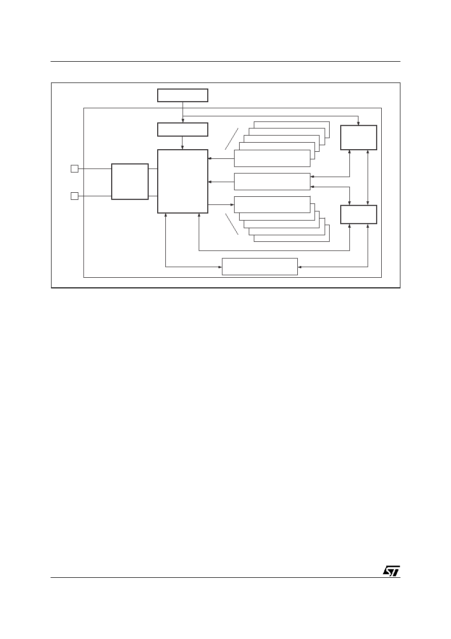
uPSD34xx - USB INTERFACE
124/264
Figure 49. USB Module Block Diagram
Basic USB Concepts
The Universal Serial Bus (USB) is more complex
than the standard serial port and requires familiar-
ity with the specification to fully understand how to
use the USB peripheral in the uPSD34xx. The
USB specification is available on the Internet
at http://www.usb.org. Some basic concepts will
be presented in this section but knowledge of the
USB specification is required.
In a USB system, there is only one master and the
master is the host computer. The host controls all
activity on the bus and devices respond to re-
quests from the host. The only exception is when
a device has been put into a low power suspend
mode by the host. In this case, the device can sig-
nal a remote wakeup. Outside of that exception, all
activity is controlled and initiated by the host. The
host-centric model versus a peer-to-peer model
provides the best way to develop low cost periph-
erals by keeping the complex control logic on the
host side. The uPSD34xx is a peripheral (non-
host) device.
Communication Flow. The USB provides a
means for communication between host (client)
software and a function on a USB device. Func-
tions can have different requirements for the com-
munication flow depending on the client software
to the USB function interaction. With USB, the var-
ious communication flows are separated to pro-
vide better bus utilization. For example, one
communication flow is used for managing the de-
vice while another is for transferring data related to
the operation of the device. Some bus access is
used for each communication flow with each flow
terminated at an endpoint on a device. Each end-
point has various aspects associated with the
communication flow. A USB device looks like a
collection of endpoints to the USB system.
8032
MCU
USB SFRs
USB
Transceiver
Serial
Interface
Engine
PLL
Clock
CTRL and Data
CTRL and Data
CTRL
CTRL
XDATA
D≠
D+
USB≠
USB+
S
F
R
B
u
s
AI10488
Endpoint4
3 - 40MHz
48MHz
Endpoint0
Endpoint4
Endpoint0
IN FIFOs (64 bytes each)
OUT FIFOs (64 bytes each)
SETUP Command
Buffer (8 bytes)
FIFO Interface Logic

125/264
uPSD34xx - USB INTERFACE
Endpoints. Each USB device contains a collec-
tion of independent endpoints, with an endpoint
being the destination of a communication flow be-
tween client software and the device. By design,
each USB device's endpoints are given specific
unique identifiers called endpoint numbers. In ad-
dition, each endpoint has an associated direction
for the data flow, either in (from device to host) or
out (from host to device). At the time a device is
connected to the USB, it is assigned a unique ad-
dress. The combination of the device address,
endpoint number, and direction allows each end-
point to be uniquely referenced.
Each endpoint has some associated characteris-
tics for the communication flow with the client soft-
ware running on the host. Those characteristics
include:
Endpoint number;
Frequency and latency requirements;
Bandwidth requirements;
Maximum packet size capability;
Error handling requirements;
Data transfer direction; and
Transfer type.
All USB devices are required to implement a de-
fault control method that uses both the input and
output endpoints with Endpoint zero. The USB
System Software uses this default control method
to initialize and generically manipulate the logical
device as the Default Control Pipe. Endpoint zero
is always accessible and provides access to the
device's configuration and status information as
well as some basic control access.
Additional (non-zero) endpoints provide the com-
munication flow required for the functionality of the
device. The non-zero endpoints are available for
use only after the device is configured per the nor-
mal device configuration process (see Chapter 9
of the USB specification, http://www.usb.org).
uPSD34xx - USB INTERFACE
126/264
Packets. USB transactions consist of data pack-
ets that contain special codes called Packet IDs
(PIDs). A PID signifies the kind of packet that is
being transmitted. While there are more types of
PIDs in a USB system, the uPSD34xx responds to
the three types shown in
Table 67.
Table 67. Types of Packet IDs
Figure 50.
shows an example of packets sent dur-
ing a USB transfer. The first packet is a Token
Packet with an OUT PID. The OUT PID indicates
that the host is going to send data to the ad-
dressed device's endpoint. The ADDR field con-
tains the address of the device and the ENDP field
contains the endpoint within the addressed de-
vice. The CRC5 is a Cyclic Redundancy Check for
error checking.
The data packet contains a DATA1 or DATA0 PID.
In a USB system, the host or device that is sending
data is responsible for toggling the data PID be-
tween DATA0 and DATA1. The receiving device
keeps track of the Toggle Bit and compares it with
the data PID that is received. This provides a
means for the receiving host or device to detect a
corrupted handshake packet. The Payload Data is
the data that the host is sending to the device and
the CRC16 is used for error checking.
For an OUT transaction, the host sends the token
and data packets. The receiving device sends a
handshake packet to notify the host whether it was
able to accept the packet or not. There are three
handshake PIDs as follows:
≠
ACK: this PID indicates that the device
received the data successfully.
≠
NAK: this handshake indicates that the device
was not able to receive the data (it is busy). A
NAK does not mean there was an error, since
errors are indicated by a "no handshake"
packet. When the host receives a NAK PID or
does not receive a handshake packet at all,
the host retries sending the data at a later
time.
≠
STALL: this handshake indicates that
something is wrong. For example, the host
has sent a device request that is not
understood, the host is trying to access a
resource that is not available, or something is
wrong with the device.
Figure 50. USB Packets in a USB Transfer Example
PID Type
PID Name
Token
IN, OUT, SETUP
Data
DATA0, DATA1
Handshake
ACK, NAK, STALL
Token Packet
Data Packet
Handshake Packet
OUT
ADDR
ENDP
CRC5
CRC16
ACK
Data1
Payload
Data
1
2
3
Token Packet
Data Packet
Handshake Packet
OUT
ADDR
ENDP
CRC5
CRC16
ACK
Data0
Payload
Data
4
5
6
AI10489

127/264
uPSD34xx - USB INTERFACE
Data Transfers with the Host. The host issues
OUT tokens followed by Data Tokens to send data
to a device. The device responds with an appropri-
ate handshake packet (ACK/NAK), indicating
whether it was able to receive the data. If the de-
vice does not receive the data packet OK (be-
cause there is some error), it does not respond
with a handshake packet. In the case of a NAK or
no response, the host retries sending the data at a
later time.
USB devices are not able to send data to a host
whenever they have it ready. When a device has
data ready, it loads data into its endpoint buffer,
making it ready for a transfer. The data will remain
in the buffer until the host issues an IN token to
that device's endpoint, at which time the data will
be sent. If the host receives the data OK, it follows
with an ACK handshake (a host never NAKs). If
the host did not receive the data OK, there is no
handshake packet. In this case, the device should
reload its endpoint buffer as appropriate and the
host will retry again later to retrieve the data.
Types of Transfers
The USB specification defines four types of trans-
fers, Bulk, Interrupt, Isochronous, and Control.
Note: The uPSD34xx supports all types of trans-
fers except Isochronous.
Bulk Transfers (see
Figure 51.
)
Bulk data is transferred in both directions and
is used with both IN and OUT endpoints.
Packets may be 8, 16, 32, or 64 bytes in
length. Bulk transfers occur in bursts, and are
scheduled by the host when there is available
time on the bus. While there is no guaranteed
delivery time for bulk transfers, the accuracy of
the data is guaranteed due to automatic retries
for erroneous data. Bulk transfers are typically
used for mass storage, printer, and scanner
data.
Interrupt Transfers (see
Figure 52.
)
Interrupt data is a lot like bulk data but travels
only in one direction, from the device to the
host, so only IN endpoints are used. Interrupt
data holds packet sizes ranging from 1 to 64
bytes. Interrupt endpoints have an associated
polling interval, meaning that the host sends
IN tokens at a periodic interval to the host on a
regular basis. Interrupt transfers are typically
used for human interface devices such as
keyboards, mice, and joysticks.
Figure 51. IN and OUT Bulk Transfers
Figure 52. Interrupt Transfer
Token Packet
Data Packet
Handshake Packet
IN
ADDR
ENDP
CRC5
CRC16
ACK
Data1
Payload
Data
Token Packet
Data Packet
Handshake Packet
OUT
ADDR
ENDP
CRC5
CRC16
ACK
Data1
Payload
Data
AI10490
Token Packet
Data Packet
Handshake Packet
IN
ADDR
ENDP
CRC5
CRC16
ACK
Data1
Payload
Data
AI10491
uPSD34xx - USB INTERFACE
128/264
Control Transfers (see
Figure 53.
)
Control transfers are used to configure and
send commands to a device. Control transfers
consist of two or three stages:
≠
SETUP
This stage always consists of a data
packet with eight bytes of USB CONTROL
data.
≠
DATA stage (optional)
If the CONTROL data is such that the host
is requesting information from the device,
the SETUP stage is followed by a DATA
stage. In this case, the host sends an IN
token and the device responds with the
requested data in the data packet.
≠
STATUS stage
This stage is essentially a handshake
informing the device of a successfully
completed control operation.
Enumeration. Enumeration is the process that
takes place when a device is first connected to the
USB. During enumeration, the host requests infor-
mation from the device about what it is, how many
endpoints it has, the power requirements, bus
bandwidth requirements, and what driver to load.
Once the enumeration process is complete, the
device is available for use.
The enumeration process consists of a series of
six steps as follows:
1.
When a device is first connected to the USB,
its address is zero. Upon detecting a new
device connected to the USB, the host sends
a Get_Descriptor request to address zero,
endpoint0.
2.
The device, upon receiving a Get_Descriptor
request, sends data back to the host
identifying what it is.
3.
The host resets the device and then sends a
Set_Address request. This is a unique
address that identifies it from all other devices
connected to the USB. This address remains
in effect until the device is disconnected from
the USB.
4.
The host sends more Get_Descriptor requests
to the device to gather more detailed
information about it and then loads the
specified driver.
5.
The host will setup and enable the endpoints
defined by the device.
6.
The device is now configured and ready for
use with the host communicating to the device
using the assigned address and endpoints.
Figure 53. Control Transfer
Token Packet
Data Packet
Handshake Packet
SETUP ADDR
ENDP
CRC5
CRC16
SETUP
Stage
DATA
Stage
(Optional)
STATUS
Stage
ACK
Data0
Payload
Data (8 bytes)
Token Packet
Data Packet
Handshake Packet
IN
ADDR
ENDP
CRC5
CRC16
ACK
Data1
Payload
Data
Token Packet
Data Packet
Handshake
Packet
OUT
ADDR
ENDP
CRC5
CRC16
ACK
Data1
AI10492
129/264
uPSD34xx - USB INTERFACE
Endpoint FIFOs
The uPSD34xx's USB module includes 5 end-
points and 10 FIFOs. Each endpoint has two
FIFOs with one for IN and the other for OUT trans-
actions. Each FIFO is 64 bytes long and is selec-
tively made visible in a 64-byte XDATA segment
for CPU access. For efficient data transfers, the
FIFOs may be paired for double buffering. With
double buffering, the CPU may operate on the
contents in one buffer while the SIE is transmitting
or receiving data in the paired buffer. uPSD34xx
supported endpoints and FIFOs are shown in
Ta-
ble 68.
Busy Bit (BSY) Operation. Each FIFO has a
busy bit (BSY) that indicates when the USB SIE
has ownership of the FIFO. When the SIE has
ownership of the FIFO, it is either writing data to or
reading data from the FIFO. The SIE writes data to
the FIFO when it is receiving an OUT packet and
reads data from the FIFO when it is sending data
in response to an IN packet. The CPU is only per-
mitted to access the FIFO when it is not busy and
accesses to it while busy are ignored. Once the IN
FIFO has been written with data by the CPU, the
CPU updates the USIZE register with the number
of bytes written to the FIFO. The value written to
the USIZE register tells the SIE the number of
bytes to send to the host in response to an IN
packet. Once the USIZE register is written, the
FIFOs busy bit is set and remains set until the data
has been transmitted in response to an IN packet.
The busy bit for an OUT FIFO is set as soon as the
SIE starts receiving an OUT packet from the host.
Once all the data has been received and written to
the FIFO, the SIE clears the busy bit and writes the
number of bytes received to the USIZE register.
Busy Bit and Interrupts. When the FIFO's inter-
rupt is enabled, a transition of the busy bit from a
'1' to a '0' (when ownership of the FIFO changes
from the SIE to the CPU) generates a USB inter-
rupt with the corresponding flag set. For an inter-
rupt on an IN FIFO, the CPU must fill the FIFO with
the next set of data to be sent and then update the
USIZE register with the number of bytes to send.
For an interrupt on an OUT FIFO, the CPU reads
the USIZE register to determine the number of
bytes received and then reads that number of data
bytes out of the FIFO.
Table 68. uPSD34xx Supported Endpoints
Endpoint
Function
Max packet size
(FIFO size)
Supported directions
0
Control 64
Bytes
OUT
0
Control
64 Bytes
IN
1
Bulk/Interrupt OUT
64 Bytes
OUT
1
Bulk/Interrupt IN
64 Bytes
IN
2
Bulk/Interrupt OUT
64 Bytes
OUT
2
Bulk/Interrupt IN
64 Bytes
IN
3
Bulk/Interrupt OUT
64 Bytes
OUT
3
Bulk/Interrupt IN
64 Bytes
IN
4
Bulk/Interrupt OUT
64 Bytes
OUT
4
Bulk/Interrupt In
64 Bytes
IN
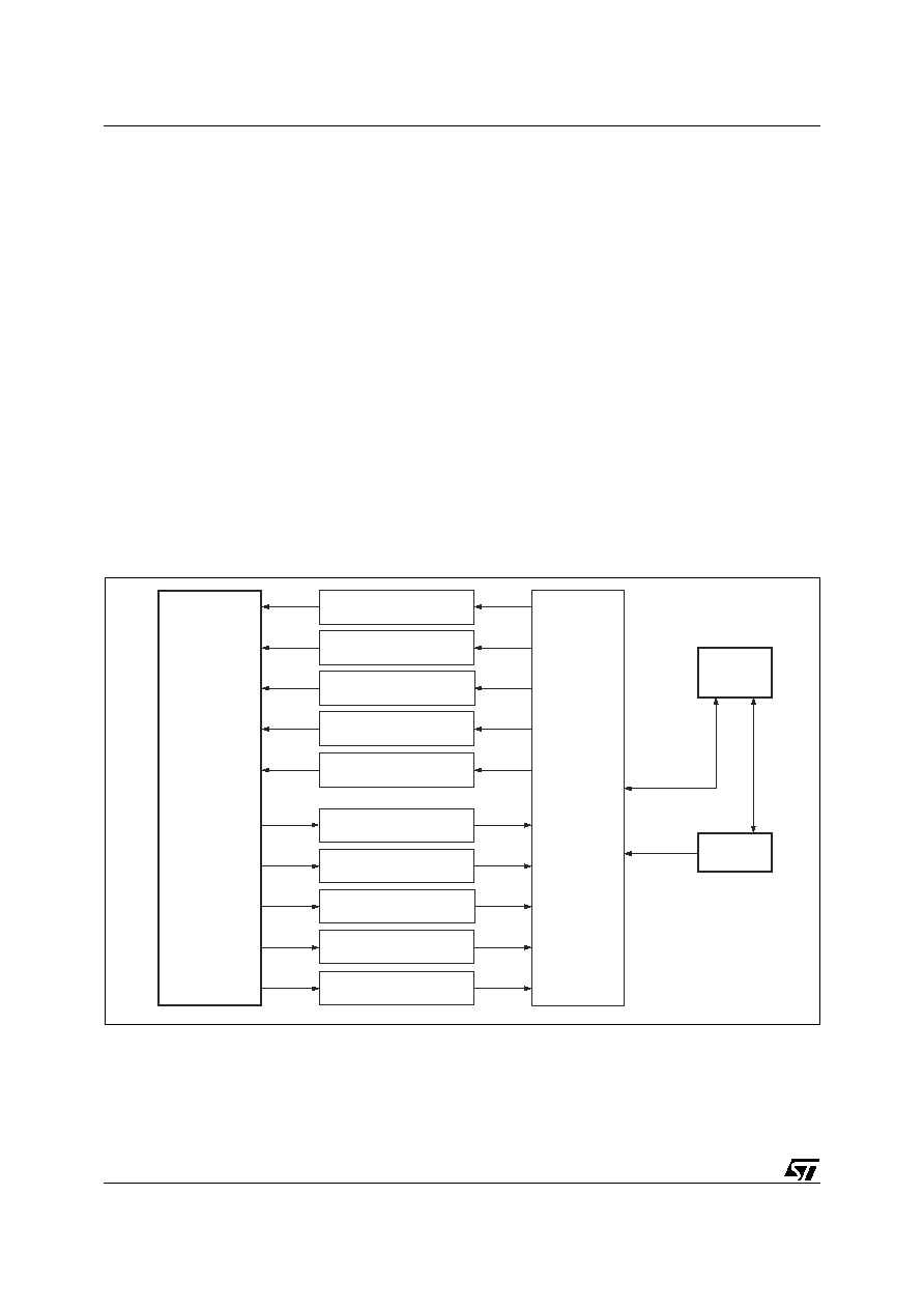
uPSD34xx - USB INTERFACE
130/264
FIFO Pairing. The FIFOs on endpoints 1 through
4 may be used independently as shown in
Figure
54.
as FIFOs with no Pairing or they may be selec-
tively paired to provide double buffering (see
Fig-
ure 55., page 131
). Double buffering provides an
efficient way to optimize data transfer rates with
bulk transfers. Double buffering allows the CPU to
process a data packet for an Endpoint while the
SIE is receiving or transmitting another packet of
data on the same Endpoint and direction. FIFO
pairing is controlled by the USB Pairing Control
Register (see UPAIR,
Table 71., page 135
). FIFO
pairing options are listed below:
IN FIFO 1 and 2
OUT FIFO 1 and 2
IN FIFO 3 and 4
OUT FIFO 3 and 4
Note: When the FIFOs are paired, the CPU must
access the odd numbered FIFO while the even
numbered FIFOs are no longer available for use.
Also when they are paired, the active FIFO is au-
tomatically toggled by the update of USIZE.
≠
Non-pairing FIFOs Example
Consider a case where the device needs to
send 1024 bytes of data to the host. Without
FIFO pairing (see
Figure 54.
), the CPU loads
the IN Endpoint0 FIFO with 64 bytes of data
and waits until the host sends an IN token to
Endpoint0, and the SIE transfers the data to
the host. Once all 64 bytes have been
transferred by the SIE, the FIFO becomes
empty and the CPU starts writing the next 64
bytes of data to the FIFO. While the CPU is
writing the data to the FIFO, the host is
sending IN tokens to Endpoint0, requesting
the next 64 bytes of data, but only gets NAKs
while the FIFO is being loaded. Once the
FIFO has been loaded by the CPU, the SIE
starts sending the data to the host with the
next IN Endpoint0 token. Again, the CPU
waits until the SIE transfers the 64 bytes of
data to the host. This is repeated until all 1024
bytes have been transferred.
Figure 54. FIFOs with no Pairing
8032
MCU
USB SFRs
Serial
Interface
Engine
CTRL
XDATA
S
F
R
B
u
s
AI10493
Endpoint4 IN FIFO
Endpoint3 IN FIFO
Endpoint2 IN FIFO
Endpoint1 IN FIFO
Endpoint0 IN FIFO
Endpoint0 OUT FIFO
Endpoint1 OUT FIFO
Endpoint2 OUT FIFO
Endpoint3 OUT FIFO
Endpoint4 OUT FIFO
FIFO
Interface
Logic
Endpoint4
Endpoint3
Endpoint2
Endpoint1
Endpoint0
Endpoint0
Endpoint1
Endpoint2
Endpoint3
Endpoint4
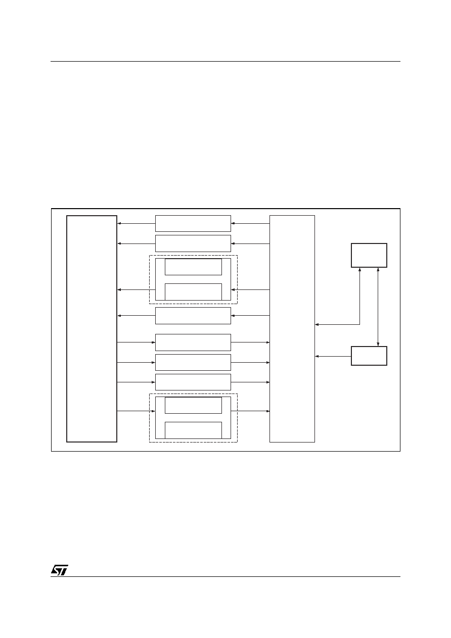
131/264
uPSD34xx - USB INTERFACE
≠
Pairing FIFOs Example
Now assume that IN Endpoint1 and Endpoint2
FIFOs are paired for double buffering and the
same 1024 bytes of data are to be transferred
to the host. As in the non-pairing example, the
CPU loads the IN Endpoint0 FIFO with 64
bytes of data. Instead of having to wait for the
SIE to transfer the 64 bytes of data to the host,
the CPU can write another 64 bytes of data to
IN Endpoint0 FIFO. While the CPU is writing
the second packet of 64 bytes of data into the
FIFO, the SIE is sending the first packet of 64
bytes of data to the host. After the CPU has
written the second packet of 64 bytes to the
FIFO, it waits a shorter amount of time for the
SIE to complete sending the first packet of
data since they were working concurrently. As
soon as the first packet is sent by the SIE, the
second packet is immediately available to be
sent by the SIE since the FIFO was already
loaded by the MCU. Also, after the first packet
is sent by the SIE, the alternate FIFO is
available for the MCU to load the third packet
of 64 bytes of data. With double buffering, the
MCU is able to always have a FIFO loaded
and ready with data to be sent by the SIE
when the host sends an IN token maximizing
the data transfer rate.
Figure 55. FIFO Pairing Example (1/2 IN Paired and 3/4 OUT Paired)
8032
MCU
USB SFRs
Serial
Interface
Engine
CTRL
XDATA
S
F
R
B
u
s
AI10494
Endpoint4 IN FIFO
Endpoint3 IN FIFO
Endpoint2 IN FIFO
P
a
i
r
e
d
P
a
i
r
e
d
Endpoint1 IN FIFO
Endpoint0 IN FIFO
Endpoint0 OUT FIFO
Endpoint1 OUT FIFO
Endpoint2 OUT FIFO
FIFO
Interface
Logic
Endpoint4
Endpoint3
Endpoint2
(not available)
Endpoint2
(not available)
Endpoint1
Endpoint0
Endpoint4
Endpoint3
Endpoint1
Endpoint0
Endpoint0
Endpoint1
Endpoint2
Endpoint3
Endpoint0
Endpoint1
Endpoint2
Endpoint3
Endpoint4
(not available)
Endpoint4
(not available)
Endpoint3 OUT FIFO
P
a
i
r
e
d
P
a
i
r
e
d
Endpoint4 OUT FIFO

uPSD34xx - USB INTERFACE
132/264
Reading and Writing FIFOs. There are a total of
ten 64-byte FIFOs. Each of the five Endpoints has
two FIFOs, one IN FIFO for IN transactions and
one OUT FIFO for OUT transactions. The FIFOs
are accessible by the CPU through a 64-byte seg-
ment in the XDATA space when the VISIBLE Bit is
set (see
Table 80., page 143
). If the VISIBLE Bit is
not set, the FIFOs are not accessible by the CPU
but are still accessible by the SIE. The base ad-
dress of the 64-byte segment is specified by the
USB Base Address High Register (see
Table
85., page 148
) and the USB Base Address Low
Register (see
Table 86., page 148
). When the
VISIBLE Bit is set, the FIFO that is accessible in
the 64-byte XDATA space segment is the FIFO
selected by the USEL register. The USEL register
contains two fields used for selecting the accessi-
ble FIFO. The EP field determines the Endpoint
selected and the DIR Bit selects the IN or OUT
FIFO associated with the Endpoint.
Accessing FIFO Control Registers, UCON, and
USIZE. Each of the 10 Endpoint FIFOs has an as-
sociated USB Endpoint Control Register (UCON,
0F1H) and a USB FIFO Valid Size Register
(USIZE, 0F2H). The USB Endpoint Select Regis-
ter (USEL) is not only used to select the Endpoint
FIFO that is accessible in the XDATA space, but
also selects the associated Endpoint's UCON and
USIZE registers that are accessible at SFR ad-
dresses 0F1H and 0F2H.
Accessing the Setup Command Buffer. Setup
Packets are sent from the host to a device's
Endpoint0 and consist of 8 bytes of command da-
ta. When the SIE receives a Setup packet from the
host, it stores the 8 bytes of data in the Command
Buffer. The command buffer is accessed via the
indexed USB Setup Command Value register (US-
CV). The USB Setup Command Index register
(USCI) is used to select the byte from the com-
mand buffer that is read when accessing the
USCV register.
USB Registers
The USB module is controlled via registers
mapped into the SFR space. The USB SFRs con-
sist of the following:
≠
UADDR: USB device address
≠
UPAIR: USB FIFO pairing control
≠
UIE0~3: USB interrupt enable
≠
UIF0~3: USB interrupt flags
≠
UCTL: USB Control
≠
USTA: USB Status
≠
USEL: USB Endpoint and direction select
≠
UCON: USB Selected FIFO control register
≠
USIZE: USB Selected FIFO size register
≠
UBASE: USB Base Address register
≠
USCI: USB Setup Command index
≠
USCV: USB Setup Command value
The memory map for the USB SFRs, the individual
bit names, and the reset values are shown in
Ta-
ble 69., page 133
.

133/264
uPSD34xx - USB INTERFACE
Table 69. uPSD34xx USB SFR Register Map
SFR
Addr
(hex)
SFR
Name
Bit Name and <Bit Address>
Reset
Value
(hex)
Comment
7
6
5
4
3
2
1
0
E2
UADDR
≠
USBADDR[6:0]
00
USB
Address
E3
UPAIR
≠
≠
≠
≠
PR3OUT PR1OUT
PR3IN
PR1IN
00
USB
Pairing
Control
E4
UIE0
≠
≠
≠
≠
RSTIE SUSPNDIE EOPIE RESUMIE
00
USB
Global
Interrupt
Enable
E5
UIE1
≠
≠
≠
IN4IE
IN3IE
IN2IE
IN1IE
IN0IE
00
USB IN
FIFO
Interrupt
Enable
E6
UIE2
≠
≠
≠
OUT4IE OUT3IE
OUT2IE
OUT1IE
OUT0IE
00
USB OUT
FIFO
Interrupt
Enable
E7
UIE3
≠
≠
≠
NAK4IE NAK3IE
NAK2IE
NAK1IE
NAK0IE
00
USB IN
FIFO NAK
Int.
Enable
E8
UIF0
GLF
INF
OUTF
NAKF
RSTF
SUSPNDF
EOPF
RESUMF
00
USB
Global
Interrupt
Flag
E9
UIF1
≠
≠
≠
IN4F
IN3F
IN2F
IN1F
IN0F
00
USB IN
FIFO
Interrupt
Flag
EA
UIF2
≠
≠
≠
OUT4F
OUT3F
OUT2F
OUT1F
OUT0F
00
USB OUT
FIFO
Interrupt
Flag
EB
UIF3
≠
≠
≠
NAK4F
NAK3F
NAK2F
NAK1F
NAK0F
00
USB IN
FIFO NAK
Int. Flag
EC
UCTL
≠
≠
≠
≠
≠
USBEN
VISIBLE WAKEUP
00
USB
Control
ED
USTA
≠
≠
≠
≠
RCVT
SETUP
IN
OUT
00
USB
Status
EE
RESERVED
EF
USEL
DIR
≠
≠
≠
≠
EP[2:0]
00
USB
Endpoint
Select
F1
UCON
≠
≠
≠
≠
ENABLE
STALL
TOGGLE
BSY
00
USB
Endpoint
Control
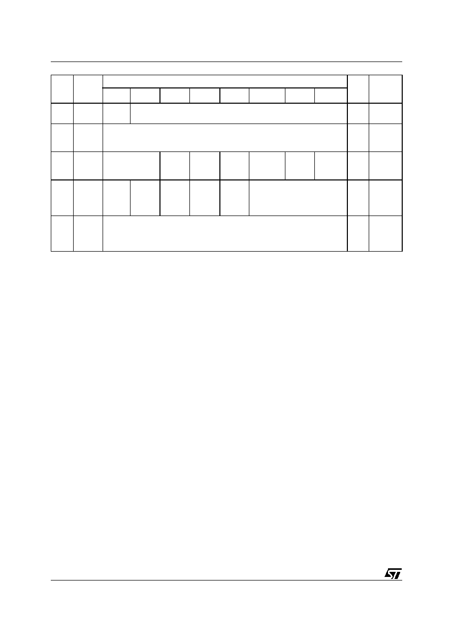
uPSD34xx - USB INTERFACE
134/264
Note: Note: Bits marked with a "≠" are Reserved.
F2
USIZE
≠
SIZE[6:0]
00
USB FIFO
Valid Size
F3
UBASEH
BASEADDR[15:8]
00
USB Base
Address
High
F4
UBASEL BASEADDR[7:6]
0
0
0
0
0
0
00
USB Base
Address
Low
F5
USCI
≠
≠
≠
≠
≠
USCI[2:0]
00
USB
Setup
Command
Index
F6
USCV
USCV[7:0]
00
USB
Setup
Command
Value
SFR
Addr
(hex)
SFR
Name
Bit Name and <Bit Address>
Reset
Value
(hex)
Comment
7
6
5
4
3
2
1
0
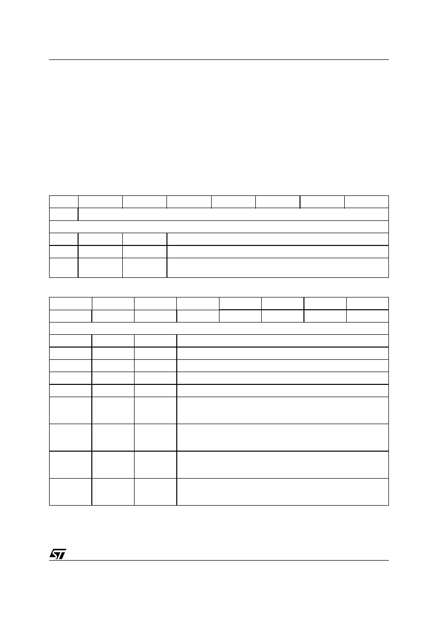
135/264
uPSD34xx - USB INTERFACE
USB Device Address Register. Initially when a
device is connected to the USB, it responds to the
host on address 0. Using the Set_Address re-
quest, the host assigns a unique address to the
device. The firmware writes this address to the
USB Device Address register (see
Table 70.
), and
subsequently the SIE only responds to transac-
tions on that assigned address. This assigned ad-
dress is in effect until the device or an upstream
hub is disconnected from the USB, the host issues
a USB Reset, or the host shuts down. The address
register is cleared with a Hardware RESET or a
USB RESET.
Endpoint FIFO Pairing. Endpoint FIFOs can be
paired for double buffering to provide an efficient
method for bulk data transfers. With double buffer-
ing enabled, the MCU can operate on one data
packet while another is being transferred over
USB.
When two FIFOs are paired, the active FIFO is au-
tomatically toggled by the update of USIZE. The
MCU must only use the odd numbered endpoint
FIFO when paired in order to access the active
FIFO. For example, if endpoints 3 and 4 OUT
FIFOs are paired, the active FIFO is accessed via
endpoint 3's OUT FIFO (see
Table 71.
).
Table 70. USB Device Address Register (UADDR 0E2h, Reset Value 00h)
Table 71. Pairing Control Register (UPAIR 0E3h, Reset Value 00h)
Bit 7
Bit 6
Bit 5
Bit 4
Bit 3
Bit 2
Bit 1
Bit 0
≠
USBADDR[6:0]
Details
Bit
Symbol
R/W
Definition
7
≠
≠
Reserved
6:0
USBADDR
R/W
USB Address of the device.
These bits are cleared with a Hardware RESET or a USB RESET.
Bit 7
Bit 6
Bit 5
Bit 4
Bit 3
Bit 2
Bit 1
Bit 0
≠
≠
≠
≠
PR3OUT
PR1OUT
PR3IN
PR1IN
Details
Bit
Symbol
R/W
Definition
7
≠
≠
Reserved
6
≠
≠
Reserved
5
≠
≠
Reserved
4
≠
≠
Reserved
3
PR3OUT
R/W
Setting this bit enables double buffering of the OUT FIFOs for Endpoints
3 and 4. Access to the double buffered FIFOs is through Endpoint3's
OUT FIFO.
2
PR1OUT
R/W
Setting this bit enables double buffering of the OUT FIFOs for Endpoints
1 and 2. Access to the double buffered FIFOs is through Endpoint1's
OUT FIFO.
1
PR3IN
R/W
Setting this bit enables double buffering of the IN FIFOs for Endpoints 3
and 4. Access to the double buffered FIFOs is through Endpoint3's IN
FIFO.
0
PR1IN
R/W
Setting this bit enables double buffering of the IN FIFOs for Endpoints 1
and 2. Access to the double buffered FIFOs is through Endpoint1's IN
FIFO.

uPSD34xx - USB INTERFACE
136/264
USB Interrupts. There are many USB related
events that generate an interrupt. The events that
generate an interrupt are selectively enabled
through the use of the USB Interrupt Enable Reg-
isters. All USB interrupts are serviced through a
single interrupt vector (see
INTERRUPT
SYSTEM, page 41
for the address of the interrupt
vector). When a USB interrupt occurs, firmware
must check the USB Interrupt Flag Registers to
determine the source of the interrupt, clear that in-
terrupt flag and process the interrupt before return-
ing to the interrupted code.
The USB interrupt priority can be set to low or
high. For the best USB response time and to max-
imize data transfer times, the USB interrupt should
be set to the highest priority (see the
INTERRUPT
SYSTEM
for the details on setting the interrupt pri-
ority).
≠
USB Reset Interrupt
The host signals a bus reset by driving both
D+ and D≠ low for at least 10ms. When the
uPSD34xx's SIE detects a reset on the USB,
it generates the RST interrupt request. When
a USB reset is detected, the USB SIE is reset.
A USB reset does not reset the CPU.
≠
USB Suspend Interrupt
If the uPSD34xx's SIE detects 3ms of no
activity on the bus, it generates the SUSPEND
interrupt request. It also causes the clock to
the SIE to shut down to conserve power. The
clock to the SIE is turned back on when a USB
Resume signal or Reset is detected.
≠
USB EOP (End of Packet) Interrupt
Every packet sent on the USB includes a
signal, called EOP, to indicate the end of the
packet. When an EOP is detected, the SIE
generates an EOP interrupt.
≠
USB Resume Interrupt
When USB activity is detected and the SIE is
in the suspend state, a RESUME interrupt is
generated and the USB clock to the SIE is
turned back on.
≠
USB Global Interrupt Enable Register (UIE0)
There are four USB events that are
considered to be global in nature, meaning
they are not specific to an endpoint, but apply
to the USB bus in general. The four global
USB events include Reset, Suspend, EOP,
and Resume.
Each event can be enabled to generate an
interrupt using the UIE0 register shown in
Table 72.
Table 72. USB Global Interrupt Enable Register (UIE0 0E4h, Reset Value 00h)
Bit 7
Bit 6
Bit 5
Bit 4
Bit 3
Bit 2
Bit 1
Bit 0
≠
≠
≠
≠
RSTIE
SUSPENDIE
EOPIE
RESUMIE
Details
Bit
Symbol
R/W
Definition
7
≠
≠
Reserved
6
≠
≠
Reserved
5
≠
≠
Reserved
4
≠
≠
Reserved
3
RSTIE
R/W
Enable the USB Reset interrupt
2
SUSPENDIE
R/W
Enable the USB Suspend interrupt
1
EOPIE
R/W
Enable the USB EOP interrupt
0
RESUMIE
R/W
Enable the USB Resume interrupt
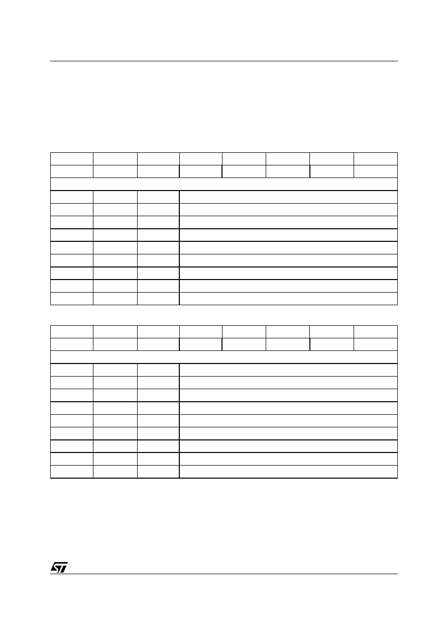
137/264
uPSD34xx - USB INTERFACE
≠
USB IN FIFO Interrupt Enable Register (UIE1)
When an endpoint's IN FIFO has been
successfully sent to the host with an IN
transaction, the FIFO becomes empty. The
UIE1 register is used to enable each
endpoint's IN FIFO interrupt (
Table 73.
).
≠
USB OUT FIFO Interrupt Enable Register
(UIE1)
When an endpoint's OUT FIFO has been filled
by an OUT transaction from the host, the FIFO
becomes full. The UIE2 register is used to
enable each endpoint's OUT FIFO interrupt
(
Table 74.
).
Table 73. USB IN FIFO Interrupt Enable Register (UIE1 0E5h, Reset Value 00h)
Table 74. USB OUT FIFO Interrupt Enable Register (UIE2 0E6h, Reset Value 00h)
Bit 7
Bit 6
Bit 5
Bit 4
Bit 3
Bit 2
Bit 1
Bit 0
≠
≠
≠
IN4IE
IN3IE
IN2IE
IN1IE
IN0IE
Details
Bit
Symbol
R/W
Definition
7
≠
≠
Reserved
6
≠
≠
Reserved
5
≠
≠
Reserved
4
IN4IE
R/W
Enable Endpoint 4 IN FIFO interrupt
3
IN3IE
R/W
Enable Endpoint 3 IN FIFO interrupt
2
IN2IE
R/W
Enable Endpoint 2 IN FIFO interrupt
1
IN1IE
R/W
Enable Endpoint 1 IN FIFO interrupt
0
IN0IE
R/W
Enable Endpoint 0 IN FIFO interrupt
Bit 7
Bit 6
Bit 5
Bit 4
Bit 3
Bit 2
Bit 1
Bit 0
≠
≠
≠
OUT4IE
OUT3IE
OUT2IE
OUT1IE
OUT0IE
Details
Bit
Symbol
R/W
Definition
7
≠
≠
Reserved
6
≠
≠
Reserved
5
≠
≠
Reserved
4
OUT4IE
R/W
Enable Endpoint 4 OUT FIFO interrupt
3
OUT3IE
R/W
Enable Endpoint 3 OUT FIFO interrupt
2
OUT2IE
R/W
Enable Endpoint 2 OUT FIFO interrupt
1
OUT1IE
R/W
Enable Endpoint 1 OUT FIFO interrupt
0
OUT0IE
R/W
Enable Endpoint 0 OUT FIFO interrupt
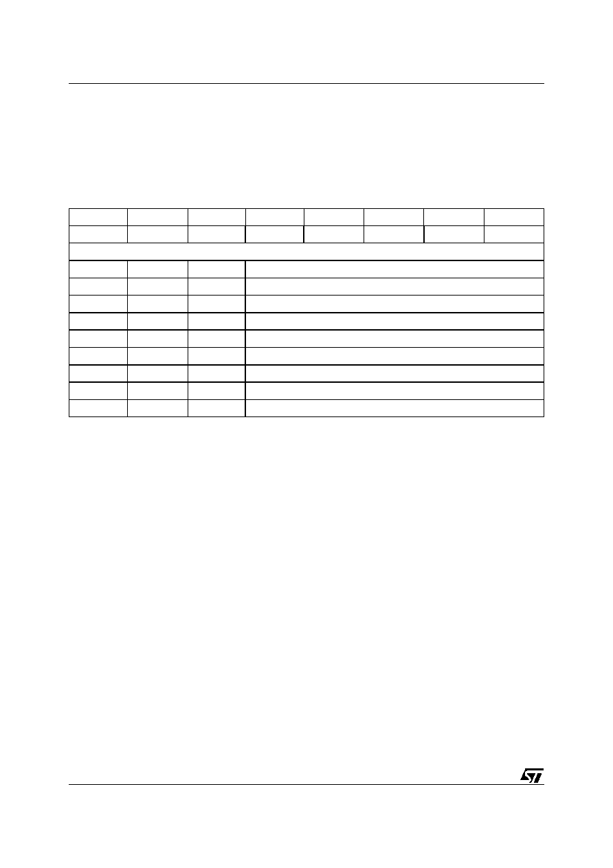
uPSD34xx - USB INTERFACE
138/264
≠
USB IN FIFO NAK Interrupt Enable Register
(UIE3)
When an endpoint's IN FIFO is empty and an
IN transaction to that endpoint has been
received, the SIE sends a NAK handshake
token since there is no data ready for it to
send.
The UIE3 register (see
Table 75.
) is used to
enable each endpoint's IN FIFO NAK
Interrupt.
Table 75. USB IN FIFO NAK Interrupt Enable Register (UIE3 0E7h, Reset Value 00h)
Bit 7
Bit 6
Bit 5
Bit 4
Bit 3
Bit 2
Bit 1
Bit 0
≠
≠
≠
NAK4IE
NAK3IE
NAK2IE
NAK1IE
NAK0IE
Details
Bit
Symbol
R/W
Definition
7
≠
≠
Reserved
6
≠
≠
Reserved
5
≠
≠
Reserved
4
NAK4IE
R/W
Enable Endpoint 4 IN FIFO NAK interrupt
3
NAK3IE
R/W
Enable Endpoint 3 IN FIFO NAK interrupt
2
NAK2IE
R/W
Enable Endpoint 2 IN FIFO NAK interrupt
1
NAK1IE
R/W
Enable Endpoint 1 IN FIFO NAK interrupt
0
NAK0IE
R/W
Enable Endpoint 0 IN FIFO NAK interrupt

139/264
uPSD34xx - USB INTERFACE
≠
USB Global Interrupt Flag Register (UIF0)
There are many different events that generate
a USB interrupt requiring a number of
registers to indicate the cause of the interrupt.
To more efficiently identify the cause of the
interrupt, the USB Global Interrupt Flag
Register (see
Table 76.
) indicates the type of
interrupt that occurred. Once the type of
interrupt is identified, the associated Interrupt
Flag Register may be read to determine the
exact cause of the interrupt.
Table 76. USB Global Interrupt Flag Register (UIF0 0E8h, Reset Value 00h)
Bit 7
Bit 6
Bit 5
Bit 4
Bit 3
Bit 2
Bit 1
Bit 0
GLF
INF
OUTF
NAKF
RSTF
SUSPENDF
EOPF
RESUMF
Details
Bit
Symbol
R/W
Definition
7
GLF
R
Global Interrupt flag
Logical OR of the RSTF, SUSPENDF, EOPF, and RESUMF interrupt flags
6
INF
R
IN FIFO Interrupt flag
Logical OR of the IN4F, IN3F, IN2F, IN1F, and IN0F interrupt flags
5
OUTF
R
OUT FIFO Interrupt flag
Logical OR of the OUT4F, OUT3F, OUT2F, OUT1F, and OUT0F interrupt
flags
4
NAKF
R
NAK FIFO Interrupt flag
Logical OR of the NAK4F, NAK3F, NAK2F, NAK1F, and NAK0F interrupt
flags
3
RSTF
R/W
USB Reset flag
This bit is set when a USB Reset is detected on the D+ and D- lines.
When a USB Reset is detected, the USB module is reset.
Note: The CPU is not reset with a USB reset.
2
SUSPENDF
R/W
USB suspend mode flag
This bit is set when the SIE detects 3ms of no activity on the bus and the
clock to the SIE is also shut down to conserve power.
1
EOPF
R/W
End of Packet flag
This bit is set when a valid End of Packet sequence is detected on the D+
and D≠ line.
0
RESUMEF
R/W
Resume flag
This bit is set when USB bus activity is detected while the SUSPNDF Bit
is set.
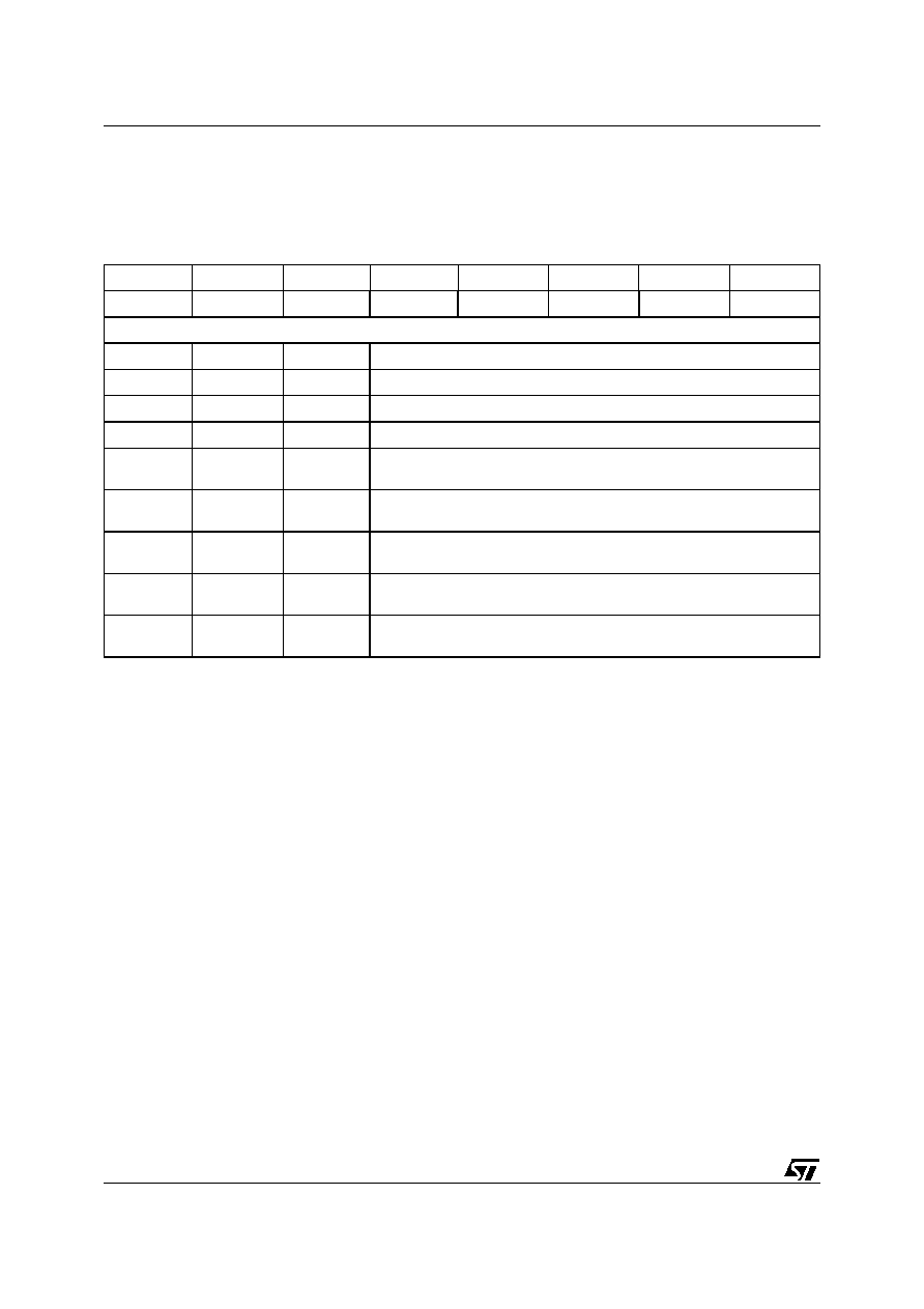
uPSD34xx - USB INTERFACE
140/264
≠
USB IN FIFO Interrupt Flag (UIF1)
The USB IN FIFO Interrupt Flag register (see
Table 77.
) contains flags that indicate when an
IN Endpoint FIFO that was full becomes
empty. Once set, firmware must clear the flag
by writing a '0' to the appropriate bit. When
FIFOs are paired, only the odd numbered
FIFO Interrupt flags are active.
Table 77. USB IN FIFO Interrupt Flag (UIF1 0E9h, Reset Value 00h)
Bit 7
Bit 6
Bit 5
Bit 4
Bit 3
Bit 2
Bit 1
Bit 0
≠
≠
≠
IN4F
IN3F
IN2F
IN1F
IN0F
Details
Bit
Symbol
R/W
Definition
7
≠
≠
Reserved
6
≠
≠
Reserved
5
≠
≠
Reserved
4
IN4F
R/W
Endpoint 4 IN FIFO Interrupt flag
This bit is set when the FIFO status changes from full to empty.
3
IN3F
R/W
Endpoint 3 IN FIFO Interrupt flag
This bit is set when the FIFO status changes from full to empty.
2
IN2F
R/W
Endpoint 2 IN FIFO Interrupt flag
This bit is set when the FIFO status changes from full to empty.
1
IN1F
R/W
Endpoint 1 IN FIFO Interrupt flag
This bit is set when the FIFO status changes from full to empty.
0
IN0F
R/W
Endpoint 0 IN FIFO Interrupt flag
This bit is set when the FIFO status changes from full to empty.

141/264
uPSD34xx - USB INTERFACE
≠
USB OUT FIFO Interrupt Flag (UIF2)
The USB OUT FIFO Interrupt Flag register
(see
Table 78.
) contains flags that indicate
when an OUT Endpoint FIFO that was empty
becomes full. Once set, firmware must clear
the flag by writing a '0' to the appropriate bit.
When FIFOs are paired, only the odd
numbered FIFO Interrupt flags are active.
Table 78. USB OUT FIFO Interrupt Flag (UIF2 0EAh, Reset Value 00h)
Bit 7
Bit 6
Bit 5
Bit 4
Bit 3
Bit 2
Bit 1
Bit 0
≠
≠
≠
OUT4F
OUT3F
OUT2F
OUT1F
OUT0F
Details
Bit
Symbol
R/W
Definition
7
≠
≠
Reserved
6
≠
≠
Reserved
5
≠
≠
Reserved
4
OUT4F
R/W
Endpoint 4 OUT FIFO Interrupt flag
This bit is set when the FIFO status changes from empty to full.
3
OUT3F
R/W
Endpoint 3 OUT FIFO Interrupt flag
This bit is set when the FIFO status changes from empty to full.
2
OUT2F
R/W
Endpoint 2 OUT FIFO Interrupt flag
This bit is set when the FIFO status changes from empty to full.
1
OUT1F
R/W
Endpoint 1 OUT FIFO Interrupt flag
This bit is set when the FIFO status changes from empty to full.
0
OUT0F
R/W
Endpoint 0 OUT FIFO Interrupt flag
This bit is set when the FIFO status changes from empty to full.
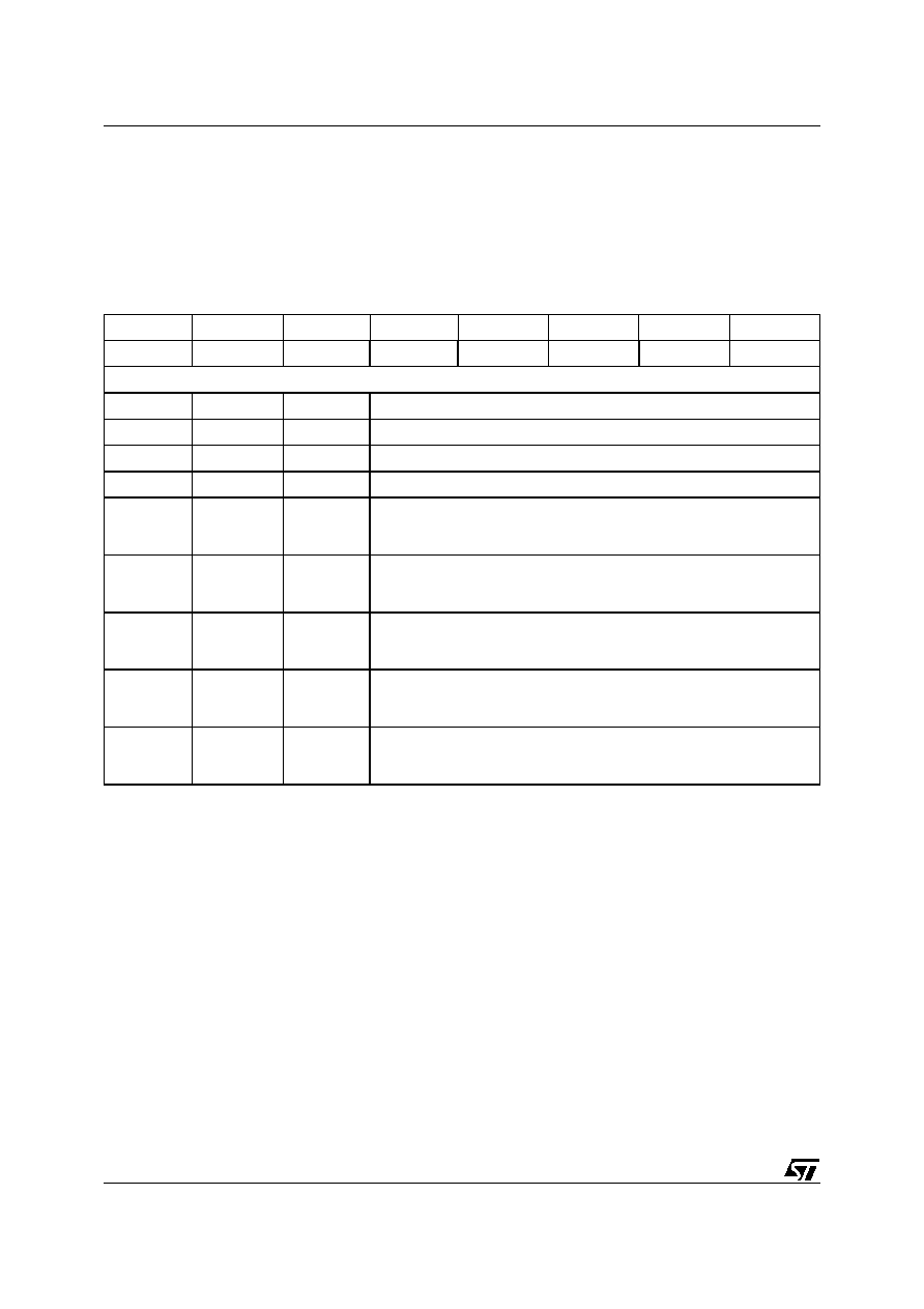
uPSD34xx - USB INTERFACE
142/264
≠
USB IN FIFO NAK Interrupt Flag (UIF3)
The USB IN FIFO NAK Interrupt Flag register
(see
Table 79.
) contains flags that indicate
when an IN Endpoint FIFO is not ready. The
Endpoint FIFO is not ready when data has not
been loaded into its FIFO and the USIZE
register has not been written to (writing to the
USIZE register puts the FIFO in a "ready" to
send data state). Until the FIFO is ready, the
SIE will continue to NAK all IN requests to the
respective Endpoint. Once set, firmware must
clear the flag by writing a '0' to the appropriate
bit. When FIFOs are paired, only the odd
numbered FIFO Interrupt Flags are active.
Table 79. USB IN FIFO NAK Interrupt Flag (UIF3 0EBh, Reset Value 00h)
Bit 7
Bit 6
Bit 5
Bit 4
Bit 3
Bit 2
Bit 1
Bit 0
≠
≠
≠
NAK4F
NAK3F
NAK2F
NAK1F
NAK0F
Details
Bit
Symbol
R/W
Definition
7
≠
≠
Reserved
6
≠
≠
Reserved
5
≠
≠
Reserved
4
NAK4F
R/W
Endpoint 4 IN FIFO NAK Interrupt flag
This bit is set when the SIE responded to an IN request with a NAK since
the FIFO was not ready.
3
NAK3F
R/W
Endpoint 3 IN FIFO NAK Interrupt flag
This bit is set when the SIE responded to an IN request with a NAK since
the FIFO was not ready.
2
NAK2F
R/W
Endpoint 2 IN FIFO NAK Interrupt flag
This bit is set when the SIE responded to an IN request with a NAK since
the FIFO was not ready.
1
NAK1F
R/W
Endpoint 1 IN FIFO NAK Interrupt flag
This bit is set when the SIE responded to an IN request with a NAK since
the FIFO was not ready.
0
NAK0F
R/W
Endpoint 0 IN FIFO NAK Interrupt flag
This bit is set when the SIE responded to an IN request with a NAK since
the FIFO was not ready.
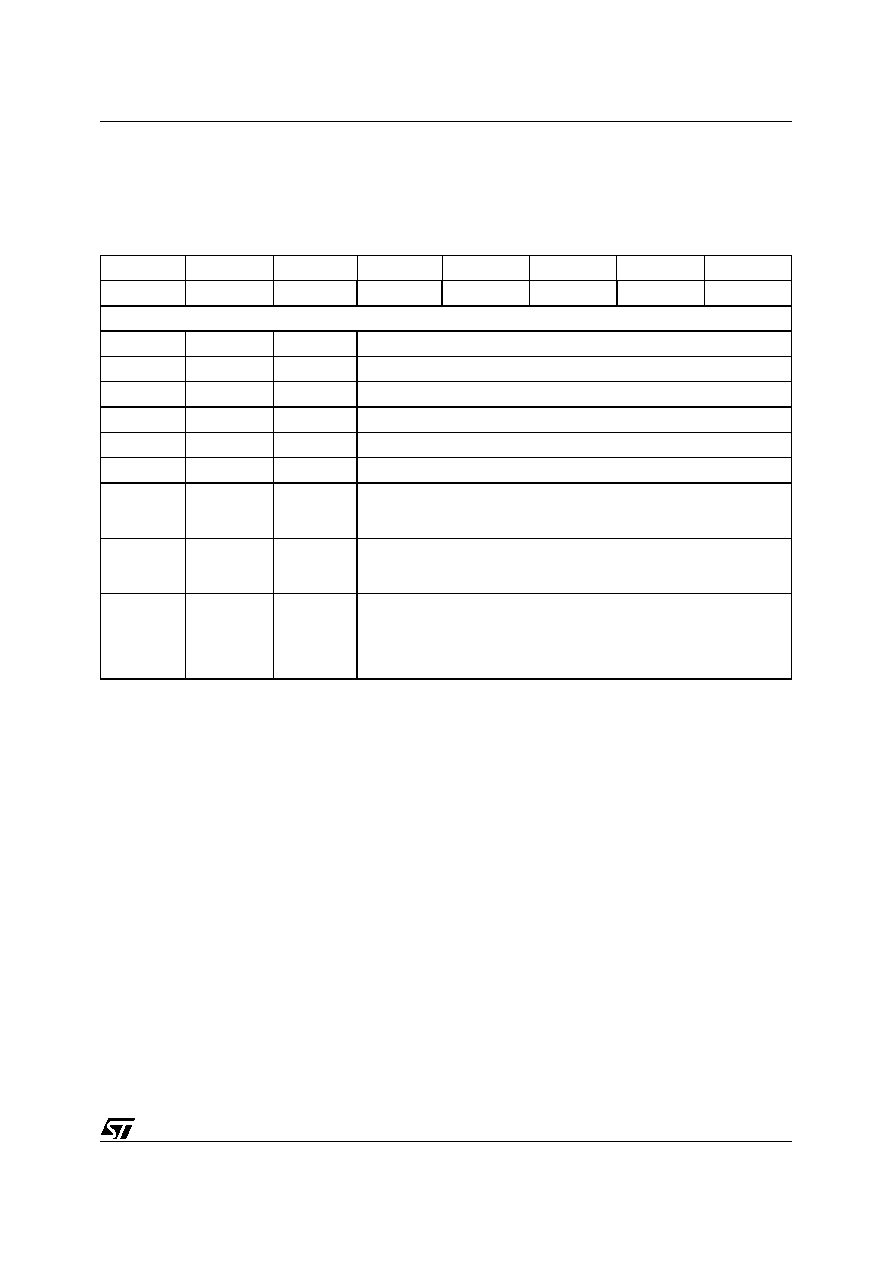
143/264
uPSD34xx - USB INTERFACE
≠
USB Control Register (UCTL)
The USB Control Register (see
Table 80.
) is
used to enable the SIE, make the Endpoint
FIFOs visible in the XDATA space and for
generating a remote wakeup signal. Upon a
reset, the USB module is disabled and must
be enabled by the CPU for communication
with the host over the USB.
Table 80. USB Control Register (UCTL 0ECh, Reset Value 00h)
Bit 7
Bit 6
Bit 5
Bit 4
Bit 3
Bit 2
Bit 1
Bit 0
≠
≠
≠
≠
≠
USBEN
VISIBLE
WAKEUP
Details
Bit
Symbol
R/W
Definition
7
≠
≠
Reserved
6
≠
≠
Reserved
5
≠
≠
Reserved
4
≠
≠
Reserved
3
≠
≠
Reserved
2
USBEN
R/W
USB Enable
When this bit is set, the USB function is enabled and the SIE responds to
tokens from the host.
1
VISIBLE
R/W
USB FIFO VISIBLE
When this bit is set, the selected USB FIFO is accessible (visible) in the
XDATA space.
0
WAKEUP
R/W
Remote Wakeup Enable
This bit forces a resume or "K" state on the USB data lines to initiate a
remote wake-up. The CPU is responsible for controlling the timing of the
forced resume that must be between 10ms and 15ms. Setting this bit will
not cause the RESUMF Bit to be set.
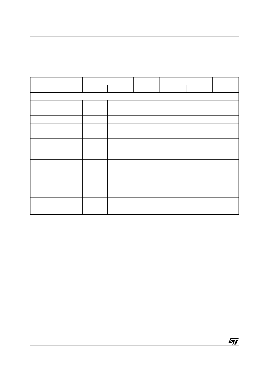
uPSD34xx - USB INTERFACE
144/264
≠
USB Endpoint0 Status (USTA)
The USB Endpoint0 Status register (see
Table
81.
) provides the status for events that occur
on the USB that are directed to endpoint0.
Table 81. USB Endpoint0 Status (USTA 0EDh, Reset Value 00h)
Bit 7
Bit 6
Bit 5
Bit 4
Bit 3
Bit 2
Bit 1
Bit 0
≠
≠
≠
≠
RCVT
SETUP
IN
OUT
Details
Bit
Symbol
R/W
Definition
7
≠
≠
Reserved
6
≠
≠
Reserved
5
≠
≠
Reserved
4
≠
≠
Reserved
3
RCVT
R
Received Data Toggle Bit
This bit indicates the toggle bit of the received data packet:
0 = Data0, and
1 = Data1
2
SETUP
R/W
SETUP Token Detect Bit
This bit is set when Endpoint0 receives a SETUP token. This bit is not
cleared when Endpoint0 receives an IN or OUT token following the
SETUP token that set this bit. This bit is cleared by software or a reset.
1
IN
R
IN Token Detect Bit
This bit is set when Endpoint0 receives an IN token. This bit is cleared
when Endpoint0 receives a SETUP or OUT token.
0
OUT
R
OUT Token Detect Bit
This bit is set when Endpoint0 receives an OUT token. This bit is cleared
when Endpoint0 receives a SETUP or IN token.
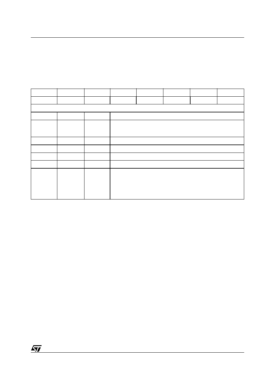
145/264
uPSD34xx - USB INTERFACE
≠
USB Endpoint Select Register (USEL)
Endpoints share the same XDATA space for
FIFOs as well as the same SFR addresses for
Control and FIFO Valid Size registers. The
USB Endpoint Select Register (see
Table 82.
)
is used to select the desired direction and
endpoint that is accessed when reading or
writing to the FIFO XDATA address space.
This register is also used to select the
direction and Endpoint when accessing the
USB Endpoint Control Register.
Table 82. USB Endpoint Select Register (USEL 0EFh, Reset Value 00h)
Bit 7
Bit 6
Bit 5
Bit 4
Bit 3
Bit 2
Bit 1
Bit 0
DIR
≠
≠
≠
≠
EP[2]
EP[1]
EP[0]
Details
Bit
Symbol
R/W
Definition
7
DIR
R/W
FIFO's Direction Select Bit:
0: IN FIFO select
1: OUT FIFO select
6
≠
≠
Reserved
5
≠
≠
Reserved
4
≠
≠
Reserved
3
≠
≠
Reserved
2:0
EP
R/W
Endpoint Selects Bits:
0: Endpoint0
1: Endpoint1
2: Endpoint2
3: Endpoint3
4: Endpoint4
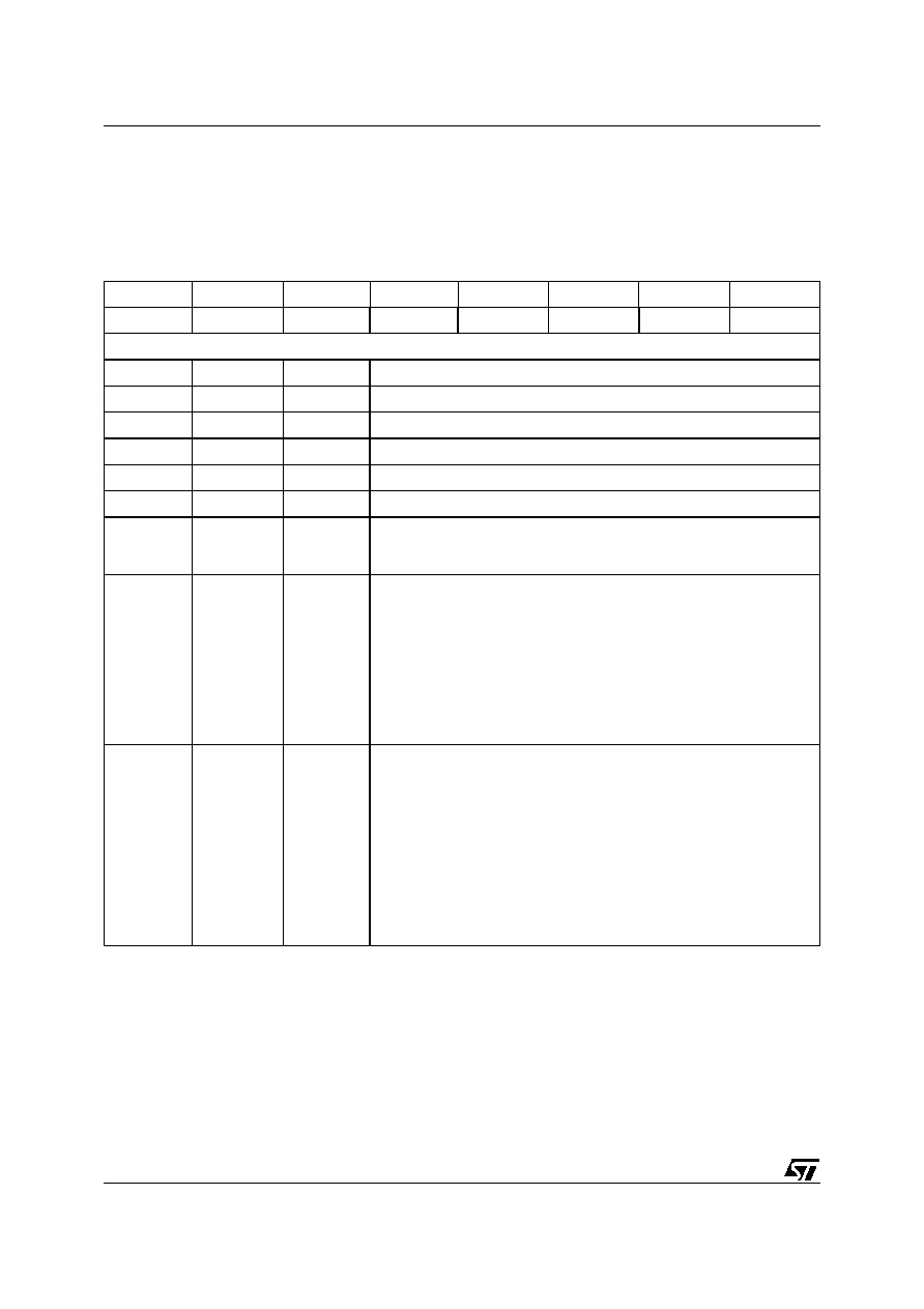
uPSD34xx - USB INTERFACE
146/264
≠
USB Endpoint Control Register (UCON)
The Endpoint selected by the USB Endpoint
Select Register (see
Table 82., page 145
)
determines the direction and FIFO (IN or OUT)
that is controlled by the USB Endpoint Control
Register (see
Table 83.
). The USB Endpoint
Control Register is used to control the
selected Endpoint and provides some status
about that Endpoint.
Table 83. USB Endpoint Control Register (UCON 0F1h, Reset Value 00h)
Bit 7
Bit 6
Bit 5
Bit 4
Bit 3
Bit 2
Bit 1
Bit 0
≠
≠
≠
≠
Enable
STALL
TOGGLE
BSY
Details
Bit
Symbol
R/W
Definition
7
≠
≠
Reserved
6
≠
≠
Reserved
5
≠
≠
Reserved
4
≠
≠
Reserved
3
ENABLE
R/W
Selected FIFO Enable Bit
2
STALL
R/W
Stall Control Bit
When this bit is set, the Endpoint returns a STALL handshake whenever it
receives an IN or OUT token.
1
TOGGLE
R/W
Data Toggle Bit
≠
Endpoint IN Case
The state of this bit determines the type of data packet (0=DATA0 or
1=DATA1) that will be sent during the next IN transaction. The CPU is
responsible for toggling this bit for every IN transaction.
≠
Endpoint OUT Case
The state of this bit indicates the type of data packet PID that was
received with the last OUT transaction (0=DATA0, 1=DATA1). The
CPU is responsible for comparing this bit with what is expected for
error detection and processing.
0
BSY
R/W
FIFO Busy Status
≠
Endpoint IN Case
Once the FIFO has been loaded and armed (USIZE written with the
number of bytes to send), the BSY Bit is set and remains set until the
SIE has transmitted the data in the FIFO. The CPU should only
access the FIFO when BSY = 0.
≠
Endpoint OUT Case
While the SIE is receiving data and storing it in the FIFO (BSY = 1), it
should not be accessed by the CPU. Once the OUT transaction is
complete (BSY=0), the CPU may read the contents of the FIFO. The
BSY Bit will remain cleared until another OUT transaction is
received.
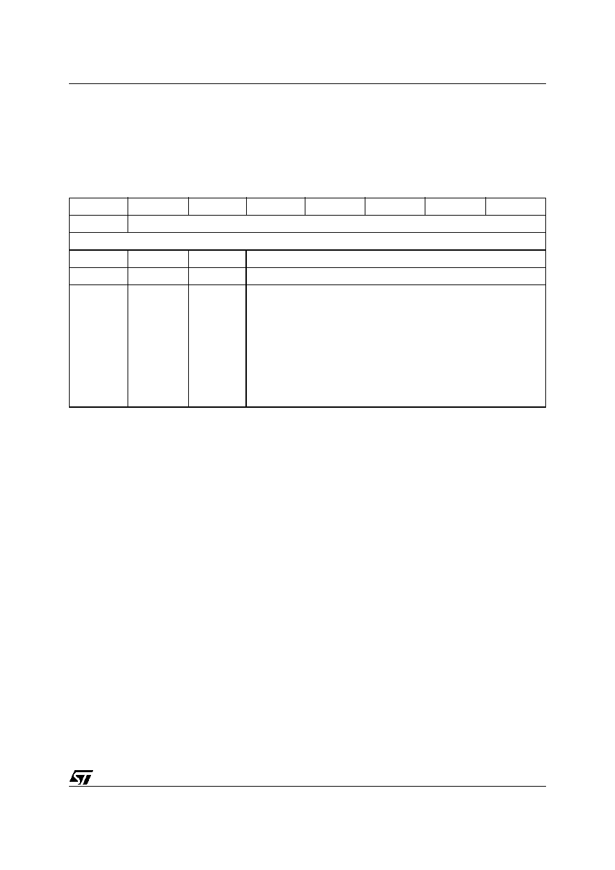
147/264
uPSD34xx - USB INTERFACE
≠
USB FIFO Valid Size (USIZE)
The Endpoint selected by the USB Endpoint
Select Register (see
Table 82., page 145
)
determines the direction and FIFO that is
controlled by the USB FIFO Valid Size (see
Table 84.
). The USB FIFO Valid Size Register
indicates the number of bytes loaded into the
IN FIFO that the SIE is to send in a Data
packet for an Endpoint IN case and indicates
the number of bytes received for an Endpoint
OUT case.
Table 84. USB FIFO Valid Size (USIZE 0F2h, Reset Value 00h)
Bit 7
Bit 6
Bit 5
Bit 4
Bit 3
Bit 2
Bit 1
Bit 0
≠
SIZE[6:0]
Details
Bit
Symbol
R/W
Definition
7
≠
≠
Reserved
6:0
SIZE
R/W
≠
Endpoint IN Case
The CPU writes the USIZE register with the number of bytes it
loaded into the IN endpoint FIFO for transmission with the next IN
transaction. Once the USIZE register has been written, the FIFO
becomes ready for transmission.
≠
Endpoint OUT Case
The CPU reads the USIZE register to determine how many bytes
were received in the data packet during the last OUT transaction.
This tells the CPU how many valid bytes to read from the FIFO.
Note: Since the FIFOs are 64 bytes in length, the maximum value for
SIZE is 64 (40h).

uPSD34xx - USB INTERFACE
148/264
≠
USB FIFO Base Address High and Low
Registers (UBASEH and UBASEL)
All 10 Endpoint FIFOs share the same 64-byte
address range. The 16-bit base address for
the FIFOs is specified using the USB Base
Address registers (see
Table 85.
and
Table
86.
). The USB Endpoint Select Register (see
Table 82., page 145
) selects the direction and
the Endpoint for the FIFO that is accessed
when addressing the 64-bytes of XDATA
space starting with the base address specified
in the Base Address Registers. The Base
Address is a 64-byte segment where the lower
6 bits of the base register are hardwired to '0.'
Important Note: The USB FIFO Base
Address must be set to an open 64-byte
segment in the XDATA space. Care should be
taken to ensure that there is no overlap of
addresses between the USB FIFOs and the
flash memory, SRAM, csiop registers, and
anything else accessed in the XDATA space.
While the logic in the PSD module handles
overlap of flash memory, SRAM, and the csiop
registers with a fixed priority (see
PSD Module
Functional Description, page 165
), this is not
the case with the USB FIFOs. Unpredictable
results as well as potential damage to the
device may occur if there is an overlap of
addresses.
Table 85. USB FIFO Base Address High Register (UBASEH 0F3h, Reset Value 00h)
Table 86. USB FIFO Base Address Low Register (UBASEL 0F4h, Reset Value 00h)
Bit 7
Bit 6
Bit 5
Bit 4
Bit 3
Bit 2
Bit 1
Bit 0
BASEADDR[15:8]
Details
Bit
Symbol
R/W
Definition
7:0
BASEADDR
[15:8]
R/W
The upper 8 bits of the 16-bit base address for USB FIFOs to be mapped
in XDATA space
Bit 7
Bit 6
Bit 5
Bit 4
Bit 3
Bit 2
Bit 1
Bit 0
BASEADDR[7:6]
0
0
0
0
0
0
Details
Bit
Symbol
R/W
Definition
7:6
BASEADDR
[7:6]
R/W
Bits 7 and 6 of the 16-bit base address for the USB FIFOs to be mapped
in XDATA space
5:0
BASEADDR
[5:0]
R
Hardwired '0'
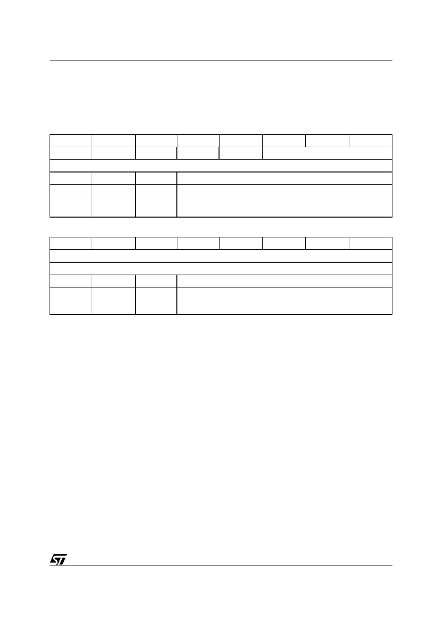
149/264
uPSD34xx - USB INTERFACE
≠
USB Setup Command Index and Value
Registers (USCI and USCV)
When a Setup/Data packet is received over
the USB, the 8 bytes of data received are
stored in a command buffer. The USB Setup
Command Index Register (see
Table 87.
)
determines which one of the eight bytes in the
buffer is read using the USB Setup Command
Value Register (see
Table 88.
).
Table 87. USB Setup Command Index Register (USCI 0F5h, Reset Value 00h)
Table 88. USB Setup Command Value Register (USCV 0F6h, Reset Value 00h)
Bit 7
Bit 6
Bit 5
Bit 4
Bit 3
Bit 2
Bit 1
Bit 0
≠
≠
≠
≠
≠
USCI[2:0]
Details
Bit
Symbol
R/W
Definition
7:3
≠
≠
Reserved
2:0
USCI[2:0]
R/W
Index to access one of the 8 bytes of USB Setup Command Data
received with the last Setup transaction
Bit 7
Bit 6
Bit 5
Bit 4
Bit 3
Bit 2
Bit 1
Bit 0
USCV[7:0]
Details
Bit
Symbol
R/W
Definition
7:0
USCV
R/W
The nth byte of the 8 bytes of USB Setup Command Data received with
the last Setup transaction. The nth byte that is read from this register is
specified by the index value in the USCI register.
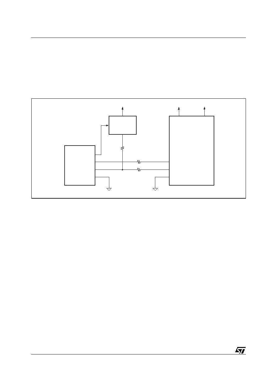
uPSD34xx - USB INTERFACE
150/264
Typical Connection to USB
Connecting the uPSD34xx to the USB is simple
and straightforward.
Figure 56.
shows a typical
self-powered example requiring only three resis-
tors and a USB power detection circuit. The USB
power detection circuit detects when the device
has been connected to the USB. When V
BUS
is de-
tected, it switches 3.3V to the pull-up resistor on
the D+ line. Per the USB specification, the pull-up
resistor on D+ is required to signal to the upstream
USB port when a full speed device has been con-
nected to the bus. The resistors in series in the D+
and D≠ lines are recommended per the USB spec-
ification to reduce transients on the data lines.
Figure 56. Typical Self Powered Example
USB Power
Detection Block
22
VBUS
VCC
D≠
D+
GND
USB≠
USB+
GND
VCC
VDD
VCC
VDD
22
USB
uPSD34xx
1.5K
+3.3V
AI10495
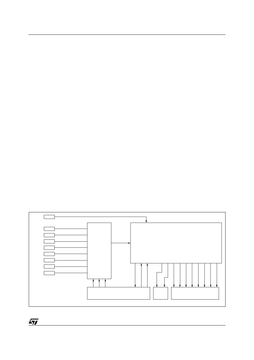
151/264
uPSD34xx - ANALOG-TO-DIGITAL CONVERTOR (ADC)
ANALOG-TO-DIGITAL CONVERTOR (ADC)
The ADC unit in the uPSD34xx is a SAR type ADC
with an SAR register, an auto-zero comparator
and three internal DACs. The unit has 8 input
channels with 10-bit resolution. The A/D converter
has its own V
REF
input (80-pin package only),
which specifies the voltage reference for the A/D
operations. The analog to digital converter (A/D)
allows conversion of an analog input to a corre-
sponding 10-bit digital value. The A/D module has
eight analog inputs (P1.0 through P1.7) to an 8x1
multiplexor. One ADC channel is selected by the
bits in the configuration register. The converter
generates a 10-bits result via successive approxi-
mation. The analog supply voltage is connected to
the V
REF
input, which powers the resistance lad-
der in the A/D module.
The A/D module has 3 registers, the control regis-
ter ACON, the A/D result register ADAT0, and the
second A/D result register ADAT1. The ADAT0
Register stores Bits 0.. 7 of the converter output,
Bits 8.. 9 are stored in Bits 0..1 of the ADAT1 Reg-
ister. The ACON Register controls the operation of
the A/D converter module. Three of the bits in the
ACON Register select the analog channel inputs,
and the remaining bits control the converter oper-
ation.
ADC channel pin input is enabled by setting the
corresponding bit in the P1SFS0 and P1SFS1
Registers to '1' and the channel select bits in the
ACON Register.
The ADC reference clock (ADCCLK) is generated
from f
OSC
divided by the divider in the ADCPS
Register. The ADC operates within a range of 2 to
16MHz, with typical ADCCLK frequency at 8MHz.
The conversion time is 4µs typical at 8MHz.
The processing of conversion starts when the
Start Bit ADST is set to '1.' After one cycle, it is
cleared by hardware. The ADC is monotonic with
no missing codes. Measurement is by continuous
conversion of the analog input. The ADAT Regis-
ter contains the results of the A/D conversion.
When conversion is complete, the result is loaded
into the ADAT. The A/D Conversion Status Bit
ADSF is set to '1.' The block diagram of the A/D
module is shown in Figure
57
. The A/D status bit
ADSF is set automatically when A/D conversion is
completed and cleared when A/D conversion is in
process.
In addition, the ADC unit sets the interrupt flag in
the ACON Register after a conversion is complete
(if AINTEN is set to '1'). The ADC interrupts the
CPU when the enable bit AINTEN is set.
Port 1 ADC Channel Selects
The P1SFS0 and P1SFS1 Registers control the
selection of the Port 1 pin functions. When the
P1SFS0 Bit is '0,' the pin functions as a GPIO.
When bits are set to '1,' the pins are configured as
alternate functions. A new P1SFS1 Register se-
lects which of the alternate functions is enabled.
The ADC channel is enabled when the bit in
P1SFS1 is set to '1.'
Note: In the 52-pin package, there is no individual
V
REF
pin because V
REF
is combined with AV
CC
pin.
Figure 57. 10-Bit ADC
ANALOG
MUX
SELECT
ADC OUT - 10 BITS
ADAT 0 REG
ACON REG
CONTROL
10-BIT SAR ADC
ADAT1
REG
ADC0
ADC1
ADC2
ADC3
ADC4
ADC5
ADC6
ADC7
AVREF
P1.0
P1.1
P1.2
P1.3
P1.4
P1.5
P1.6
P1.7
AVREF
AI07856

uPSD34xx - ANALOG-TO-DIGITAL CONVERTOR (ADC)
152/264
Table 89. ACON Register (SFR 97h, Reset Value 00h)
Bit 7
Bit 6
Bit 5
Bit 4
Bit 3
Bit 2
Bit 1
Bit 0
AINTF
AINTEN
ADEN
ADS2
ADS1
ADS0
ADST
ADSF
Details
Bit
Symbol
Function
7
AINTF
ADC Interrupt flag. This bit must be cleared with software.
0 = No interrupt request
1 = The AINTF flag is set when ADSF goes from '0' to '1.' Interrupts CPU when both
AINTF and AINTEN are set to '1.'
6
AINTEN
ADC Interrupt Enable
0 = ADC interrupt is disabled
1 = ADC interrupt is enabled
5
ADEN
ADC Enable Bit
0 = ADC shut off and consumes no operating current
1 = Enable ADC. After ADC is enabled, 16ms of calibration is needed before ADST Bit is
set.
4.. 2
ADS2.. 0
Analog channel Select
000 Select channel 0 (P1.0)
001 Select channel 0 (P1.1)
010 Select channel 0 (P1.2)
011 Select channel 0 (P1.3)
101 Select channel 0 (P1.5)
110 Select channel 0 (P1.6)
111 Select channel 0 (P1.7)
1
ADST
ADC Start Bit
0 = Force to zero
1 = Start ADC, then after one cycle, the bit is cleared to '0.'
0
ADSF
ADC Status Bit
0 = ADC conversion is not completed
1 = ADC conversion is completed. The bit can also be cleared with software.
153/264
uPSD34xx - ANALOG-TO-DIGITAL CONVERTOR (ADC)
Table 90. ADCPS Register Details (SFR 94h, Reset Value 00h)
Table 91. ADAT0 Register (SFR 95h, Reset Value 00h)
Table 92. ADAT1 Register (SFR 96h, Reset Value 00h)
Bit
Symbol
Function
7:4
≠
Reserved
3
ADCCE
ADC Conversion Reference Clock Enable
0 = ADC reference clock is disabled (default)
1 = ADC reference clock is enabled
2:0
ADCPS[2:0]
ADC Reference Clock PreScaler
Only three Prescaler values are allowed:
ADCPS[2:0] = 0, for f
OSC
frequency 16MHz or less. Resulting ADC clock is f
OSC
.
ADCPS[2:0] = 1, for f
OSC
frequency 32MHz or less. Resulting ADC clock is f
OSC
/2.
ADCPS[2:0] = 2, for f
OSC
frequency 32MHz > 40MHz. Resulting ADC clock is f
OSC
/4.
Bit
Symbol
Function
7:0
≠
Store ADC output, Bit 7 - 0
Bit
Symbol
Function
7:2
≠
Reserved
1.. 0
≠
Store ADC output, Bit 9, 8

uPSD34xx - PROGRAMMABLE COUNTER ARRAY (PCA) WITH PWM
154/264
PROGRAMMABLE COUNTER ARRAY (PCA) WITH PWM
There are two Programmable Counter Array
blocks (PCA0 and PCA1) in the uPSD34xx. A PCA
block consists of a 16-bit up-counter, which is
shared by three TCM (Timer Counter Module). A
TCM can be programmed to perform one of the
following four functions:
1.
Capture Mode: capture counter values by
external input signals
2.
Timer Mode
3.
Toggle Output Mode
4.
PWM Mode: fixed frequency (8-bit or 16-bit),
programmable frequency (8-bit only)
PCA Block
The 16-bit Up-Counter in the PCA block is a free-
running counter (except in PWM Mode with pro-
grammable frequency). The Counter has a choice
of clock input: from an external pin, Timer 0 Over-
flow, or PCA Clock.
A PCA block has 3 Timer Counter Modules (TCM)
which share the 16-bit Counter output. The TCM
can be configured to capture or compare counter
value, generate a toggling output, or PWM func-
tions. Except for the PWM function, the other TCM
functions can generate an interrupt when an event
occurs.
Every TCM is connected to a port pin in Port 4; the
TCM pin can be configured as an event input, a
PWMs, a Toggle Output, or as External Clock In-
put. The pins are general I/O pins when not as-
signed to the TCM.
The TCM operation is configured by Control regis-
ters and Capture/Compare registers.
Table
93., page 155
lists the SFR registers in the PCA
blocks.
Figure 58. PCA0 Block Diagram
TIMER0
OVERFLOW
P4.3/ECI
PCACH0
8-bit
PCACL0
8-bit
CLKSEL1
IDLE MODE
(From CPU)
OVF0
INT
EOVFI
TCM0
TCM1
TCM2
PWM FREQ
COMPARE
P4.0/CEX0
P4.1/CEX1
P4.2/CEX2
16-bit up Timer/Counter
CLKSEL0
PCAIDLE
PCA0CLK
CLEAR COUNTER
EN_PCA
EN_ALL
AI07857
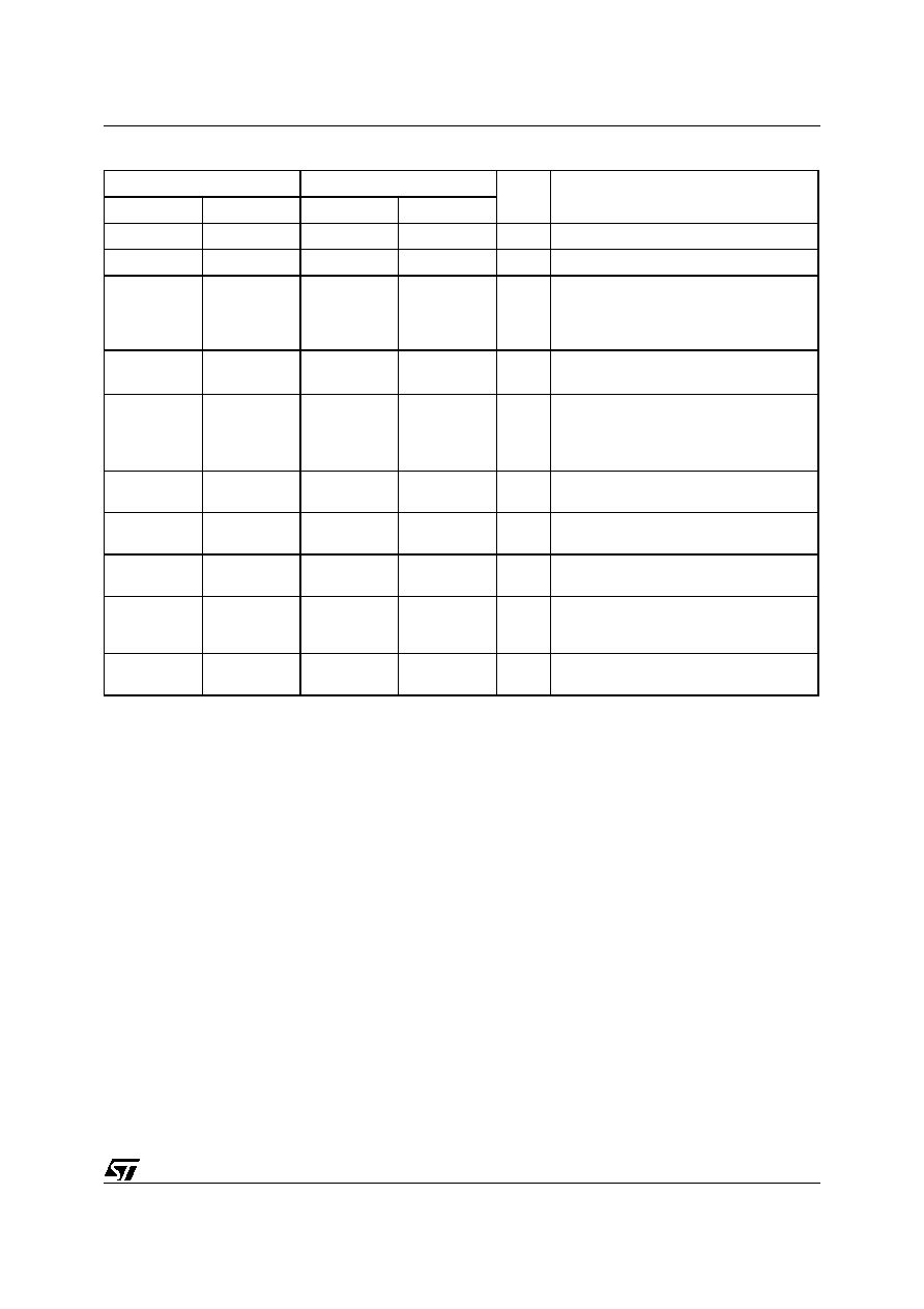
155/264
uPSD34xx - PROGRAMMABLE COUNTER ARRAY (PCA) WITH PWM
Table 93. PCA0 and PCA1 Registers
SFR Address
Register Name
RW
Register Function
PCA0
PCA1
PCA0
PCA1
A2
BA
PCACL0
PCACL1
RW
The low 8 bits of PCA 16-bit counter.
A3
BB
PCACH0
PCACH1
RW
The high 8 bits of PCA 16-bit counter.
A4
BC
PCACON0
PCACON1
RW
Control Register
≠
Enable PCA, Timer Overflow flag ,
PCA Idle Mode, and Select clock
source.
A5
A5
PCASTA
N/A
RW
Status Register, Interrupt Status flags
≠
Common for both PCA Block 0 and 1.
A9,
AA,
AB
BD,
BE,
BF
TCMMODE0
TCMMODE1
TCMMODE2
TCMMODE3
TCMMODE4
TCMMODE5
RW
TCM Mode
≠
Capture, Compare, and Toggle
Enable Interrupts
≠
PWM Mode Select.
AC
AD
C1
C2
CAPCOML0
CAPCOMH0
CAPCOML3
CAPCOMH3
RW
Capture/Compare registers of TCM0
AF
B1
C3
C4
CAPCOML1
CAPCOMH1
CAPCOML4
CAPCOMH4
RW
Capture/Compare registers of TCM1
B2
B3
C5
C6
CAPCOML2
CAPCOMH2
CAPCOML5
CAPCOMH5
RW
Capture/Compare registers of TCM2
B4
C7
PWMF0
PWMF1
RW
The 8-bit register to program the PWM
frequency. This register is used for
programmable, 8-bit PWM Mode only.
FB
FC
CCON2
CCON3
RW
Specify the pre-scaler value of PCA0 or
PCA1 clock input
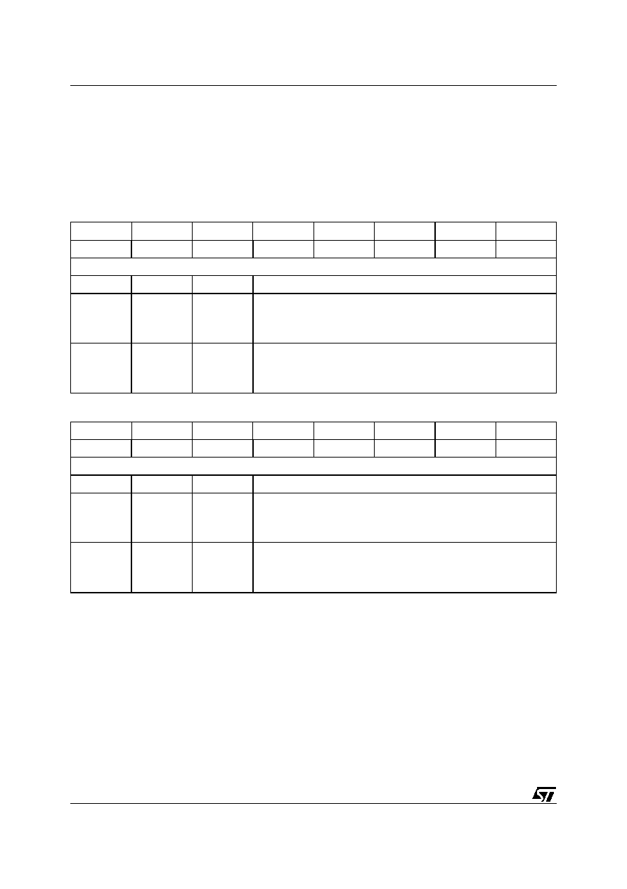
uPSD34xx - PROGRAMMABLE COUNTER ARRAY (PCA) WITH PWM
156/264
PCA Clock Selection
The clock input to the 16-bit up counter in the PCA
block is user-programmable. The three clock
sources are:
≠
PCA Prescaler Clock (PCA0CLK, PCA1CLK)
≠
Timer 0 Overflow
≠
External Clock, Pin P4.3 or P4.7
The clock source is selected in the configuration
register PCACON. The Prescaler output clock
PCACLK is the f
OSC
divided by the divisor which is
specified in the CCON2 or CCON3 Register.
When External Clock is selected, the maximum
clock frequency should not exceed f
OSC
/4.
Table 94. CCON2 Register Bit Definition (SFR 0FBh, Reset Value 10h)
Table 95. CCON3 Register Bit Definition (SFR 0FCh, Reset Value 10h)
Bit 7
Bit 6
Bit 5
Bit 4
Bit 3
Bit 2
Bit 1
Bit 0
≠
≠
≠
PCA0CE
PCA0PS3
PCA0PS2
PCA0PS1
PCA0PS0
Details
Bit
Symbol
R/W
Definition
4
PCA0CE
R/W
PCA0 Clock Enable
0 = PCA0CLK is disabled
1 = PCA0CLK is enabled (default)
3:0
PCA0PS
[3:0]
R/W
PCA0 Prescaler
f
PCA0CLK
= f
OSC
/ (2 ^ PCA0PS[3:0])
Divisor range: 1, 2, 4, 8, 16... 16384, 32768
Bit 7
Bit 6
Bit 5
Bit 4
Bit 3
Bit 2
Bit 1
Bit 0
≠
≠
≠
PCA1CE
PCA1PS3
PCA1PS2
PCA1PS1
PCA1PS0
Details
Bit
Symbol
R/W
Definition
4
PCA1CE
R/W
PCA1 Clock Enable
0 = PCA1CLK is disabled
1 = PCA1CLK is enabled (default)
3:0
PCA1PS
[3:0]
R/W
PCA1 Prescaler
f
PCA1CLK
= f
OSC
/ (2 ^ PCA1PS[3:0])
Divisor range: 1, 2, 4, 8, 16... 16384, 32768
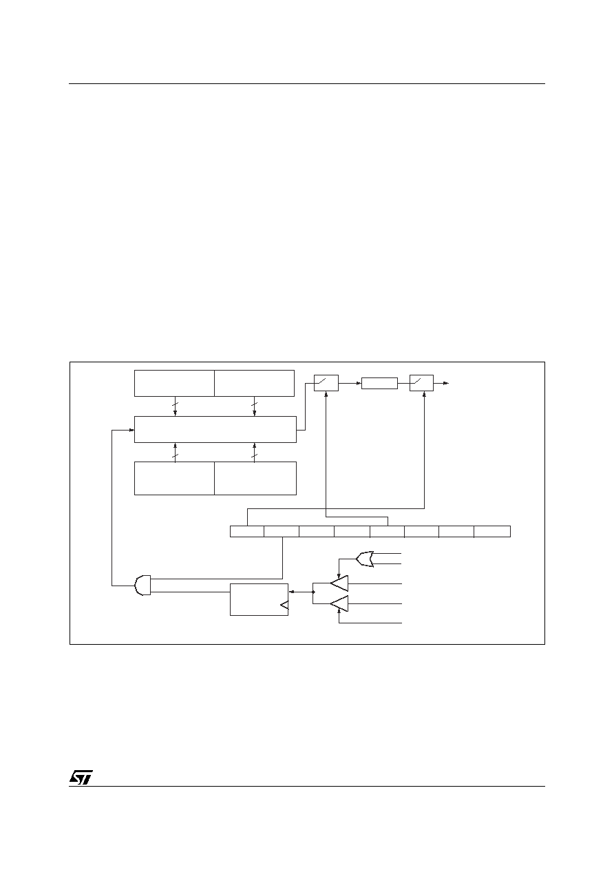
157/264
uPSD34xx - PROGRAMMABLE COUNTER ARRAY (PCA) WITH PWM
Operation of TCM Modes
Each of the TCM in a PCA block supports four
modes of operation. However, an exception is
when the TCM is configured in PWM Mode with
programmable frequency. In this mode, all TCM in
a PCA block must be configured in the same mode
or left to be not used.
Capture Mode
The CAPCOM registers in the TCM are loaded
with the counter values when an external pin input
changes state. The user can configure the counter
value to be loaded by positive edge, negative edge
or any transition of the input signal. At loading, the
TCM can generate an interrupt if it is enabled.
Timer Mode
The TCM modules can be configured as software
timers by enable the comparator. The user writes
a value to the CAPCOM registers, which is then
compared with the 16-bit counter. If there is a
match, an interrupt can be generated to CPU.
Toggle Mode
In this mode, the user writes a value to the TCM's
CAPCOM registers and enables the comparator.
When there is a match with the Counter output, the
output of the TCM pin toggles. This mode is a sim-
ple extension of the Timer Mode.
PWM Mode - (X8), Fixed Frequency
In this mode, one or all the TCM's can be config-
ured to have a fixed frequency PWM output on the
port pins. The PWM frequency depends on when
the low byte of the Counter overflows (modulo
256). The duty cycle of each TCM module can be
specified in the CAPCOMHn Register. When the
PCA_Counter_L value is equal to or greater than
the value in CAPCOMHn, the PWM output is
switched to a high state. When the
PCA_Counter_L Register overflows, the content
in CAPCOMHn is loaded to CAPCOMLn and a
new PWM pulse starts.
Figure 59. Timer Mode
Note: m = 0: n = 0, 1, or 2
m = 1: n = 3, 4, or 5
MATCH_TIMER
INTR
0
0
0
TCMMODEn
ENABLE
8
8
MATCH
PCASTA
CAPCOMLn
PCACLm
PCACHm
16-bit COMPARATOR
CAPCOMHn
INTFn
0
0
16-bit up Timer/Counter
8
8
EINTF
E_COMP CAP_PE
CAP_NE
MATCH
TOGGLE
PWM1
PWM0
RESET
WRITE to
CAPCOMHn
WRITE to
CAPCOMLn
1
0
EN_FLAG
D
C
AI07858
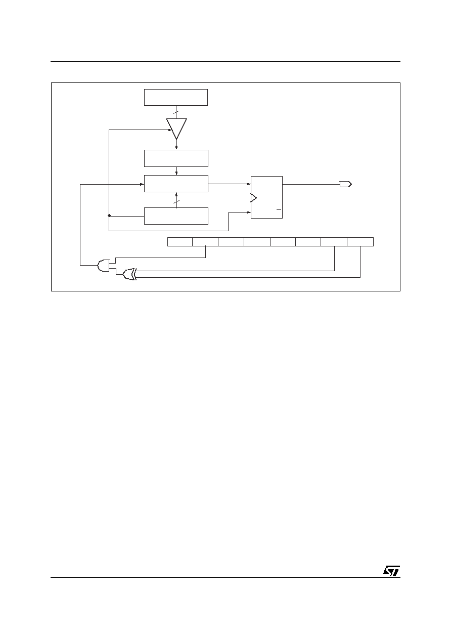
uPSD34xx - PROGRAMMABLE COUNTER ARRAY (PCA) WITH PWM
158/264
Figure 60. PWM Mode - (X8), Fixed Frequency
Note: m = 0: n = 0, 1, or 2
m = 1: n = 3, 4, or 5
CAPCOMHn
OVERFLOW
ENABLE
8
PCACLm
8
CAPCOMLn
8-bit COMPARATORn
CEXn
MATCH
S
R
Q
Q
SET
CLR
0
0
TCMMODEn
0
0
0
EINTF
E_COMP CAP_PE
CAP_NE
MATCH
TOGGLE
PWM1
PWM0
AI07859
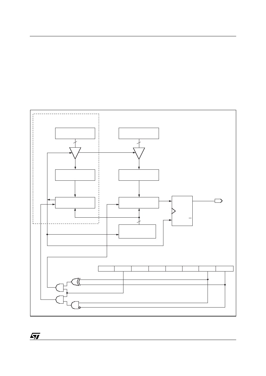
159/264
uPSD34xx - PROGRAMMABLE COUNTER ARRAY (PCA) WITH PWM
PWM Mode - (X8), Programmable Frequency
In this mode, the PWM frequency is not deter-
mined by the overflow of the low byte of the
Counter. Instead, the frequency is determined by
the PWMFm Register. The user can load a value
in the PWMFm Register, which is then compared
to the low byte of the Counter. If there is a match,
the Counter is cleared and the Load registers
(PWMFm, CAPCOMHn) are re-loaded for the next
PWM pulse. There is only one PWMFm Register
which serves all 3 TCM in a PCA block.
If one of the TCM modules is operating in this
mode, the other modules in the PCA must be con-
figured to the same mode or left not to be used.
The duty cycle of the PWM can be specified in the
CAPCOMHn Register as in the PWM with fixed
frequency mode. Different TCM modules can have
their own duty cycle.
Note: The value in the Frequency Register (PWM-
Fm) must be larger than the duty cycle register
(CAPCOM).
Figure 61. PWM Mode - (X8) Programmable Frequency
Note: m = 0: n = 0, 1, or 2
m = 1: n = 3, 4, or 5
CLR
PCACHm
PWM FREQ COMPARE
PWMFm = PCACLm
PCACLm
CAPCOMHn
CEXn
ENABLE
ENABLE
8
8
PWMFm
8-bit COMPARATORm
8-bit COMPARATORn
CAPCOMLn
MATCH
S
R
Q
Q
SET
CLR
8
0
0
TCMMODEn
0
0
0
EINTF
E_COMP CAP_PE
CAP_NE
MATCH
TOGGLE
PWM1
PWM0
AI07860
uPSD34xx - PROGRAMMABLE COUNTER ARRAY (PCA) WITH PWM
160/264
PWM Mode - Fixed Frequency, 16-bit
The operation of the 16-bit PWM is the same as
the 8-bit PWM with fixed frequency. In this mode,
one or all the TCM can be configured to have a
fixed frequency PWM output on the port pins. The
PWM frequency is depending on the clock input
frequency to the 16-bit Counter. The duty cycle of
each TCM module can be specified in the CAP-
COMHn and CAPCOMLn Registers. When the 16-
bit PCA_Counter is equal or greater than the val-
ues in registers CAPCOMHn and CAPCOMLn, the
PWM output is switched to a high state. When the
PCA_Counter overflows, CEXn is asserted low.
PWM Mode - Fixed Frequency, 10-bit
The 10-bit PWM logic requires that all 3 TCMs in
PCA0 or PCA1 operate in the same 10-bit PWM
mode. The 10-bit PWM operates in a similar man-
ner as the 16-bit PWM, except the PCACHm and
PCACLm counters are reconfigured as 10-bit
counters. The CAPCOMHn and CAPCOMLn Reg-
isters become 10-bit registers.
PWM duty cycle of each TCM module can be
specified in the 10-bit CAPCOMHn and CAP-
COMLn Registers. When the 10-bit PCA counter
is equal or greater than the values in the 10-bit
registers CAPCOMHn and CAPCOMLn, the PWM
output switches to a high state. When the 10-bit
PCA counter overflows, the PWM pin is switched
to a logic low and starts the next PWM pulse.
The most-significant 6 bits in the PCACHm
counter and CAPCOMH Register are "Don't cares"
and have no effect on the PWM generation.
Writing to Capture/Compare Registers
When writing a 16-bit value to the PCA Capture/
Compare registers, the low byte should always be
written first. Writing to CAPCOMLn clears the
E_COMP Bit to '0'; writing to CAPCOMHn sets
E_COMP to '1' the largest duty cycle is 100%
(CAPCOMHn CAPCOMLn = 0x0000), and the
smallest duty cycle is 0.0015% (CAPCOMHn
CAPCOMLn = 0xFFFF). A 0% duty cycle may be
generated by clearing the E_COMP Bit to `0'.
Control Register Bit Definition
Each PCA has its own PCA_CONFIGn, and each
module within the PCA block has its own
TCM_Mode Register which defines the operation
of that module (see
Table 96., page 160
through
Table 97., page 161
). There is one PCA_STATUS
Register that covers both PCA0 and PCA1 (see
Table 98., page 162
).
Table 96. PCA0 Control Register PCACON0 (SFR 0A4h, Reset Value 00h)
Bit 7
Bit 6
Bit 5
Bit 4
Bit 3
Bit 2
Bit 1
Bit 0
EN-ALL
EN_PCA
EOVFI
PCAIDLE
≠
≠
CLK_SEL[1:0]
Details
Bit
Symbol
Function
7
EN-ALL
0 = No impact on TCM modules
1 = Enable both PCA counters simultaneously (override the EN_PCA Bits)
This bit is to start the two 16-bit counters in the PCA. For customers who want 5 PWM,
for example, this bit can start all of the PWM outputs.
6
EN_PCA
0 = PCA counter is disabled
1 = PCA counter is enabled
EN_PCA Counter Run Control Bit. Set with software to turn the PCA counter on. Must
be cleared with software to turn the PCA counter off.
5
EOVFI
1 = Enable Counter Overflow Interrupt if overflow flag (OVF) is set
4
PCAIDLE
0 = PCA operates when CPU is in Idle Mode
1 = PCA stops running when CPU is in Idle Mode
3
≠
Reserved
2
10B_PWM
0 = Select 16-bit PWM
1 = Select 10-bit PWM
1-0
CLK_SEL
[1:0]
00 Select Prescaler clock as Counter clock
01 Select Timer 0 Overflow
10 Select External Clock pin (P4.3 for PCA0) (MAX clock rate = f
OSC
/4)
161/264
uPSD34xx - PROGRAMMABLE COUNTER ARRAY (PCA) WITH PWM
Table 97. PCA1 Control Register PCACON1 (SFR 0BCh, Reset Value 00h)
Bit 7
Bit 6
Bit 5
Bit 4
Bit 3
Bit 2
Bit 1
Bit 0
≠
EN_PCA
EOVFI
PCAIDLE
≠
≠
CLK_SEL[1:0]
Details
Bit
Symbol
Function
6
EN_PCA
0 = PCA counter is disabled
1 = PCA counter is enabled
EN_PCA Counter Run Control Bit. Set with software to turn the PCA counter on. Must
be cleared with software to turn the PCA counter off.
5
EOVFI
1 = Enable Counter Overflow Interrupt if overflow flag (OVF) is set
4
PCAIDLE
0 = PCA operates when CPU is in Idle Mode
1 = PCA stops running when CPU is in Idle Mode
3
≠
Reserved
2
10B_PWM
0 = Select 16-bit PWM
1 = Select 10-bit PWM
1-0
CLK_SEL
[1:0]
00 Select Prescaler clock as Counter clock
01 Select Timer 0 Overflow
10 Select External Clock pin (P4.7 for PCA1) (MAX clock rate = f
OSC
/4)

uPSD34xx - PROGRAMMABLE COUNTER ARRAY (PCA) WITH PWM
162/264
Table 98. PCA Status Register PCASTA (SFR 0A5h, Reset Value 00h)
Bit 7
Bit 6
Bit 5
Bit 4
Bit 3
Bit 2
Bit 1
Bit 0
OVF1
INTF5
INTF4
INTF3
OVF0
INTF2
INTF1
INTF0
Details
Bit
Symbol
Function
7
OFV1
PCA1 Counter OverFlow flag
Set by hardware when the counter rolls over. OVF1 flags an interrupt if Bit EOVFI in
PCACON1 is set. OVF1 may be set with either hardware or software but can only be
cleared with software.
6
INTF5
TCM5 Interrupt flag
Set by hardware when a match or capture event occurs.
Must be clear with software.
5
INTF4
TCM4 Interrupt flag
Set by hardware when a match or capture event occurs.
Must be clear with software.
4
INTF3
TCM3 Interrupt flag
Set by hardware when a match or capture event occurs.
Must be clear with software.
3
OVF0
PCA0 Counter OverFlow flag
Set by hardware when the counter rolls over. OVF0 flags an interrupt if Bit EOVFI in
PCACON0 is set. OVF1 may be set with either hardware or software but can only be
cleared with software.
2
INTF2
TCM2 Interrupt flag
Set by hardware when a match or capture event occurs.
Must be clear with software.
1
INTF1
TCM1 Interrupt flag
Set by hardware when a match or capture event occurs.
Must be clear with software.
0
INTF0
TCM0 Interrupt flag
Set by hardware when a match or capture event occurs.
Must be clear with software.
163/264
uPSD34xx - PROGRAMMABLE COUNTER ARRAY (PCA) WITH PWM
TCM Interrupts
There are 8 TCM interrupts: 6 match or capture in-
terrupts and two counter overflow interrupts. The 8
interrupts are "ORed" as one PCA interrupt to the
CPU.
By the nature of PCA application, it is unlikely that
many of the interrupts occur simultaneously. If
they do, the CPU has to read the interrupt flags
and determine which one to serve. The software
has to clear the interrupt flag in the Status Register
after serving the interrupt.
Table 99. TCMMODE0 - TCMMODE5 (6 Registers, Reset Value 00h)
Table 100. TCMMODE Register Configurations
Note: 1. 10-bit PWM mode requires the 10B_PWM Bit in the PCACON Register set to '1.'
Bit 7
Bit 6
Bit 5
Bit 4
Bit 3
Bit 2
Bit 1
Bit 0
EINTF
E_COMP
CAP_PE
CAP_NE
MATCH
TOGGLE
PWM[1:0]
Details
Bit
Symbol
Function
7
EINTF
1 - Enable the interrupt flags (INTF) in the Status Register to generate an interrupt.
6
E_COMP
1 - Enable the comparator when set
5
CAP_PE
1 - Enable Capture Mode, a positive edge on the CEXn pin.
4
CAP_NE
1 - Enable Capture Mode, a negative edge on the CEXn pin.
3
MATCH
1 - A match from the comparator sets the INTF bits in the Status Register.
2
TOGGLE
1 - A match on the comparator results in a toggling output on CEXn pin.
1-0
PWM[1:0]
01 Enable PWM Mode (x8), fixed frequency. Enable the CEXn pin as a PWM output.
10 Enable PWM Mode (x8) with programmable frequency. Enable the CEXn pin as a
PWM output.
11 Enable PWM Mode (x10 or x16), fixed frequency. Enable the CEXn pin as a PWM
output.
EINTF
E_COMP CAP_PE
CAP_NE
MATCH
TOGGLE
PWM1
PWM0
TCM FUNCTION
0
0
0
0
0
0
0
0
No operation (reset value)
0
1
0
0
0
0
0
1
8-bit PWM, fixed frequency
0
1
0
0
0
0
1
0
8-bit PWM, programmable
frequency
0
1
0
0
0
0
1
1
10-bit or 16-bit PMW, fixed
frequency
(1)
X
1
0
0
1
1
0
0
16-bit toggle
X
1
0
0
1
0
0
0
16-bit Software Timer
X
X
0
1
0
0
0
0
16-bit capture, negative trigger
X
X
1
0
0
0
0
0
16-bit capture, positive trigger
X
X
1
1
0
0
0
0
16-bit capture, transition trigger
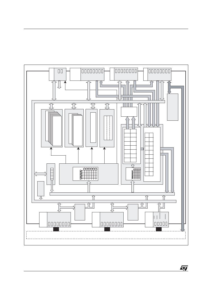
uPSD34xx - PSD MODULE
164/264
PSD MODULE
The PSD Module is stacked with the MCU Module
to form the uPSD34xx, see
HARDWARE
DESCRIPTION, page 14
. Details of the PSD Mod-
ule are shown in Figure
62
. The two separate
modules interface with each other at the 8032 Ad-
dress, Data, and Control interface blocks in Figure
62
.
Figure 62. PSD Module Block Diagram
PD1
PD2
POR
T D
PA
0
PA
1
PA
2
PA
3
PA
4
PA
5
PA
6
PA
7
PB0
PB1
PB2
PB3
PB4
PB5
PB6
PB7
POR
T B
GENERAL PLD
20 INPUT
MA
CR
OCELLS
16 OUTPUT MA
CR
OCELLS
A
B
A
B
A
B
A
B
A
B
A
B
A
B
A
B
B
C
B
C
B
C
B
C
B
C
B
C
B
C
B
C
SECURITY
LOCK
PLD INPUT BU
S
PIN FEEDBA
C
K
NODE FEEDBA
CK
PSD Module:
uPSD34xx
DECODE
PLD
AND-OR
ARRA
Y
FS0-7
AA
A
A
A
A
A
A
BB
B
B
B
B
B
B
C
C
C
C
T
O
PLD
INPUT
BU
S
PC0
PC1
PC2
PC3
PC4
PC5
PC6
PC7
POR
T C
JT
A
G-ISP T
O
ALL
AREAS OF PSD
MODULE
ADDR,
D
A
T
A
,
CONTR
OL B
U
S LINKED
T
O
8032 MCU
R
UNTIME CONTR
OL,
256 REGs
GPIO
, VM,
P
A
GE
PO
WER MNGMT
CSIOP
PLD
CSBOO
T0-3
EXTERNAL
CHIP-
SELECTS
MAIN FLASH MEMOR
Y
Up to 8 SEGMENTS
Up to 256 KBytes
T
O
T
AL
FS0
FS7
2nd FLASH MEMOR
Y
Up to 4 SEGMENTS
Up to 32 KBytes
T
O
T
AL
CSBOO
T0
CSBOO
T
3
D
ATA
Lo
w
Address
Latch
D
ATA
High
Address
Latch
A0-A7
A8-A15
8032 MUX
ADDR/D
A
T
A
AD0
AD1
AD2
AD3
AD4
AD5
AD6
AD7
8032 MUX
ADDR/D
A
T
A
AD8
AD9
AD10
AD11
AD12
AD13
AD14
AD15
8032
Contr
ol
PSEN
ALE
RD
WR
RST
8032 MCU Module
POR
T A
(80-pin
onl
y)
T
O
JT
A
G
DEB
UG ON MCU
GPIO
PLD
GPIO
GPIO
GPIO
8 PIN INPUTS
MCU READ or
WRITE
MCU READ
PLD OUT
PLD OUT
PLD OUT
PLD OUT
PLD OUT
JT
A
G
CNTL
8 PIN INPUTS
4 PIN INPUTS
MCU
READ or
WRITE
RS0
Up to 8 KBytes
SRAM
P
A
GE REG
JT
A
G
OMC
ALLO-
CA
T
O
R
AND-OR
ARRA
Y
69 INPUTS
69 INPUTS
AI10454
PLD INPUT BUS

165/264
uPSD34xx - PSD MODULE
PSD Module Functional Description
Major functional blocks are shown in
Figure
62., page 164
. The next sections describe each
major block.
8032 Address/Data/Control Interface. These
signals attach directly to the MCU Module to im-
plement a 16-bit multiplexed 8051-style bus be-
tween the two stacked die. The MCU instruction
prefetch and branch cache logic resides on the
MCU Module, leaving a modified 8051-style mem-
ory interface on the PSD Module.
The active-low reset signal originating from the
MCU Module goes to the PSD Module reset input
(RST). This reset signal can then be routed as an
external output from the uPSD34xx to the system
PC board, if needed, through any one of the PLD
output pins as active-high or active-low logic by
specifying logic equations in PSDsoft Express.
The 8032 address and data busses are routed
throughout the PSD Module as shown in Figure
62
connecting many elements on the PSD Module to
the 8032 MCU. The 8032 bus is not only connect-
ed to the memories, but also to the General PLD,
making it possible for the 8032 to directly read and
write individual logic macrocells inside the General
PLD.
Dual Flash Memories and IAP. uPSD34xx de-
vices contain two independent Flash memory ar-
rays. This means that the 8032 can read
instructions from one Flash memory array while
erasing or writing the other Flash memory array.
Concurrent operation like this enables robust re-
mote updates of firmware, also known as In-Appli-
cation Programming (IAP). IAP can occur using
any uPSD34xx interface (e.g., UART, I2C, SPI).
Concurrent memory operation also enables the
designer to emulate EEPROM memory within ei-
ther of the two Flash memory arrays for small data
sets that have frequent updates.
The 8032 can erase Flash memories by individual
sectors or it can erase an entire Flash memory ar-
ray at one time. Each sector in either Flash mem-
ory may be individually write protected, blocking
any WRITEs from the 8032 (good for boot and
start-up code protection). The Flash memories au-
tomatically go to standby between 8032 READ or
WRITE accesses to conserve power. Minimum
erase cycles is 100K and minimum data retention
is 15 years. Flash memory, as well as the entire
PSD Module may be programmed with the JTAG
In-System Programming (ISP) interface with no
8032 involvement, good for manufacturing and lab
development.
Main Flash Memory. The Main Flash memory is
divided into equal sized sectors that are individual-
ly selectable by the Decode PLD output signals,
named FSx, one signal for each Main Flash mem-
ory sector. Each Flash sector can be located at
any address within 8032 program address space
(accessed with PSEN) or data address space,
also known as 8032 XDATA space (accessed with
RD or WR), as defined with the software develop-
ment tool, PSDsoft Express. The user only has to
specify an address range for each segment and
specify if Main Flash memory will reside in 8032
data or program address space, and then PSEN,
RD, or WR are automatically activated for the
specified range. 8032 firmware is easily pro-
grammed into Main Flash memory using PSDsoft
Express or other software tools. See
Table
101., page 166
for Main Flash sector sizes on the
various uPSD34xx devices.
Secondary Flash Memory. The smaller Second-
ary Flash memory is also divided into equal sized
sectors that are individually selectable by the De-
code PLD signals, named CSBOOTx, one signal
for each Secondary Flash memory sector. Each
sector can be located at any address within 8032
program address space (accessed with PSEN) or
XDATA space (accessed with RD or WR) as de-
fined with PSDsoft Express. The user only has to
specify an address range for each segment, and
specify if Secondary Flash memory will reside in
8032 data or program address space, and then
PSEN, RD, or WR are automatically activated for
the specified range. 8032 firmware is easily pro-
grammed into Secondary Flash memory using PS-
Dsoft Express and others. See
Table
101., page 166
for Secondary Flash sector sizes.
SRAM. The SRAM is selected by a single signal,
named RS0, from the Decode PLD. SRAM may be
located at any address within 8032 XDATA space
(accessed with RD or WR). These choices are
specified using PSDSoft Express, where the user
specifies an SRAM address range. See
Table
101., page 166
for SRAM sizes.
The SRAM may optionally be backed up by an ex-
ternal battery (or other DC source) to make its con-
tents non-volatile (see
SRAM Standby Mode
(battery backup), page 224
).

uPSD34xx - PSD MODULE
166/264
Table 101. uPSD34xx Memory Configuration
Runtime Control Registers, csiop. A block of
256 bytes is decoded inside the PSD Module for
module control and status (see
Table
106., page 176
). The base address of these 256
locations is referred to in this data sheet as csiop
(Chip Select I/O Port), and is selected by the De-
code PLD output signal, CSIOP. The csiop regis-
ters are always viewed by the 8032 as XDATA,
and are accessed with RD and WR signals. The
address range of csiop is specified using PSDsoft
Express where the user only has to specify an ad-
dress range of 256 bytes, and then the RD or WR
signals are automatically activated for the speci-
fied range. Individual registers within this block are
accessed with an offset from the specified csiop
base address. 39 registers are used out of the 256
locations to control the output state of I/O pins, to
read I/O pins, to set the memory page, to control
8032 program and data address space, to control
power management, to READ/WRITE macrocells
inside the General PLD, and other functions during
runtime. Unused locations within csiop are re-
served and should not be accessed.
Memory Page Register. 8032 MCU architecture
has an inherent size limit of 64K bytes in either
program address space or XDATA space. Some
uPSD34xx devices have much more memory that
64K, so special logic such as this page register is
needed to access the extra memory. This 8-bit
page register (Figure
63
) can be loaded and read
by the 8032 at runtime as one of the csiop regis-
ters. Page register outputs feed directly into both
PLDs creating extended address signals used to
"page" memory beyond the 64K byte limit (pro-
gram space or XDATA). Most 8051 compilers di-
rectly support memory paging, also known as
memory banking. If memory paging is not needed,
or if not all eight page register bits are needed for
memory paging, the remaining bits may be used in
the General PLD for general logic. Page Register
outputs are cleared to logic '0' at reset and power-
up.
Programmable Logic (PLDs) . The uPSD34xx
contains two PLDs (
Figure 74., page 188
) that
may optionally run in Turbo or Non-Turbo mode.
PLDs operate faster (less propagation delay)
while in Turbo mode but consume more power
than in Non-Turbo mode. Non-Turbo mode allows
the PLDs to go to standby automatically when no
PLD inputs are changing to conserve power.
The logic configuration (from equations) of both
PLDs is stored with non-volatile Flash technology
and the logic is active upon power-up. PLDs may
NOT be programmed by the 8032, PLD program-
ming only occurs through the JTAG interface.
Figure 63. Memory Page Register
Device
Main Flash Memory
Secondary Flash Memory
SRAM
Total
Flash Size
(bytes)
Individual
Sector Size
(bytes)
Number of
Sectors (Sector
Select Signal)
Total
Flash Size
(bytes)
Individual
Sector Size
(bytes)
Number of
Sectors (Sector
Select Signal)
SRAM
Size
(bytes)
uPSD3422
64K
16K
4 (FS0-3)
32K
8K
4 (CSBOOT0-3)
4K
uPSD3433
128K
16K
8 (FS0-7)
32K
8K
4 (CSBOOT0-3)
8K
uPSD3434
256K
32K
8 (FS0-7)
32K
8K
4 (CSBOOT0-3)
8K
8032
Data
Bus
Load or
Read via
csiop +
offset E0h
D0
D7
D6
D5
D4
D3
D2
D1
Q0
Q7
Q6
Q5
Q4
Q3
Q2
Q1
DPLD
and
GPLD
Page
Register
Chip-
Selects
and
General
Logic
RST
(PSD Module Reset)
RST
PGR0-7
AI09172

167/264
uPSD34xx - PSD MODULE
PLD #1, Decode PLD (DPLD). This programma-
ble logic implements memory mapping and is used
to select one of the individual Main Flash memory
segments, one of individual Secondary Flash
memory segments, the SRAM, or the group of
csiop registers when the 8032 presents an ad-
dress to DPLD inputs (see
Figure 75., page 190
).
The DPLD can also optionally drive external chip
select signals on Port D pins. The DPLD also op-
tionally produces two select signals (PSEL0 and
PSEL1) used to enable a special data bus repeat-
er function on Port A, referred to as Peripheral I/O
Mode. There are 69 DPLD input signals which in-
clude: 8032 address and control signals, Page
Register outputs, PSD Module Port pin inputs, and
GPLD logic feedback.
PLD #2, General PLD (GPLD). This program-
mable logic is used to create both combinatorial
and sequential general purpose logic (see
Figure
76., page 192
). The GPLD contains 16 Output
Macrocells (OMCs) and 20 Input Macrocells
(IMCs). Output Macrocell registers are unique in
that they have direct connection to the 8032 data
bus allowing them to be loaded and read directly
by the 8032 at runtime through OMC registers in
csiop. This direct access is good for making small
peripheral devices (shifters, counters, state ma-
chines, etc.) that are accessed directly by the 8032
with little overhead. There are 69 GPLD inputs
which include: 8032 address and control signals,
Page Register outputs, PSD Module Port pin in-
puts, and GPLD feedback.
OMCs. There are two banks of eight OMCs inside
the GPLD, MCELLAB, and MCELLBC, totalling 16
OMCs all together. Each individual OMC is a base
logic element consisting of a flip-flop and some
AND-OR logic (
Figure 77., page 193
). The gener-
al structure of the GPLD with OMCs is similar in
nature to a 22V10 PLD device with the familiar
sum-of-products (AND-OR) construct. True and
compliment versions of 69 input signals are avail-
able to the inputs of a large AND-OR array. AND-
OR array outputs feed into an OR gate within each
OMC, creating up to 10 product-terms for each
OMC. Logic output of the OR gate can be passed
on as combinatorial logic or combined with a flip-
flop within in each OMC to realize sequential logic.
OMC outputs can be used as a buried nodes driv-
ing internal feedback to the AND-OR array, or
OMC outputs can be routed to external pins on
Ports A, B, or C through the OMC Allocator.
OMC Allocator. The OMC allocator (
Figure
78., page 194
) will route eight of the OMCs from
MCELLAB to pins on either Port A or Port B, and
will route eight of the OMCs from MCELLBC to
pins on either Port B or Port C, based on what is
specified in PSDsoft Express.
IMCs. Inputs from pins on Ports A, B, and C are
routed to IMCs for conditioning (clocking or latch-
ing) as they enter the chip, which is good for sam-
pling and debouncing inputs. Alternatively, IMCs
can pass port input signals directly to PLD inputs
without clocking or latching (
Figure
79., page 198
). The 8032 may read the IMCs
asynchronously at any time through IMC registers
in csiop.
Note: The JTAG signals TDO, TDI, TCK, and TMS
on Port C do not route through IMCs, but go direct-
ly to JTAG logic.
I/O Ports. For 80-pin uPSD34xx devices, the
PSD Module has 22 individually configurable I/O
pins distributed over four ports (these I/O are in
addition to I/O on MCU Module). For 52-pin
uPSD34xx devices, the PSD Module has 13 indi-
vidually configurable I/O pins distributed over
three ports. See
Figure 85., page 212
for I/O port
pin availability on these two packages.
I/O port pins on the PSD Module (Ports A, B, C,
and D) are completely separate from the port pins
on the MCU Module (Ports 1, 3, and 4). They even
have different electrical characteristics. I/O port
pins on the PSD Module are accessed by csiop
registers, or they are controlled by PLD equations.
Conversely, I/O Port pins on the MCU Module are
controlled by the 8032 SFR registers.
Table 102. General I/O pins on PSD Module
Note: Four pins on Port C are dedicated to JTAG, leaving four pins
for general I/O.
Pkg
Port A
Port B
Port C
Port D
Total
52-pin
0
8
4
1
13
80-pin
8
8
4
2
22

uPSD34xx - PSD MODULE
168/264
Each I/O pin on the PSD Module can be individu-
ally configured for different functions on a pin-by-
pin basis (
Figure 80., page 200
). Following are the
available functions on PSD Module I/O pins.
≠
MCU I/O: 8032 controls the output state of
each port pin or it reads input state of each
port pin, by accessing csiop registers at run-
time. The direction (in or out) of each pin is
also controlled by csiop registers at run-time.
≠
PLD I/O: PSDsoft Express logic equations
and pin configuration selections determine if
pins are connected to OMC outputs or IMC
inputs. This is a static and non-volatile
configuration. Port pins connected to PLD
outputs can no longer be driven by the 8032
using MCU I/O output mode.
≠
Latched MCU Address Output: Port A or
Port B can output de-multiplexed 8032
address signals A0 - A7 on a pin-by-pin basis
as specified in csiop registers at run-time. In
addition, Port B can also be configured to
output de-multiplexed A8-A15 in PSDsoft
Express.
≠
Data Bus Repeater: Port A can bi-
directionally buffer the 8032 data bus (de-
multiplexed) for a specified address range in
PSDsoft Express. This is referred to as
Peripheral I/O Mode in this document.
≠
Open Drain Outputs: Some port pins can
function as open-drain as specified in csiop
registers at run-time.
≠
Pins on Port D can be used for external chip-
select outputs originating from the DPLD,
without consuming OMC resources within the
GPLD.
JTAG Port. In-System Programming (ISP) can
be performed through the JTAG signals on Port C.
This serial interface allows programming of the en-
tire PSD Module device or subsections of the PSD
Module (for example, only Flash memory but not
the PLDs) without the participation of the 8032. A
blank uPSD34xx device soldered to a circuit board
can be completely programmed in 10 to 25 sec-
onds. The four basic JTAG signals on Port C;
TMS, TCK, TDI, and TDO form the IEEE-1149.1
interface. The PSD Module does not implement
the IEEE-1149.1 Boundary Scan functions, but
uses the JTAG interface for ISP an 8032 debug.
The PSD Module can reside in a standard JTAG
chain with other JTAG devices and it will remain in
BYPASS mode when other devices perform JTAG
functions.
ISP programming time can be reduced as much as
30% by using two optional JTAG signals on Port
C, TSTAT and TERR, in addition to TMS, TCK,
TDI and TDO, and this is referred to as "6-pin
JTAG". The FlashLINK
JTAG
programming cable
is available from STMicroelectronics and PSDsoft
Express software is available at no charge from
www.st.com/psm. More JTAG ISP information
maybe found in the section titled "JTAG ISP and
Debug" on page 137.
The MCU module is also included in the JTAG
chain within the uPSD34xx device for 8032 debug-
ging and emulation. While debugging, the PSD
Module is in BYPASS mode. Conversely, during
ISP, the MCU Module is in BYPASS mode.
Power Management. The PSD Module has bits
in csiop registers that are configured at run-time by
the 8032 to reduce power consumption of the
GPLD. The Turbo Bit in the PMMR0 Register can
be set to logic '1' and both PLDs will go to Non-
Turbo mode, meaning it will latch its outputs and
go to sleep until the next transition on its inputs.
There is a slight penalty in PLD performance
(longer propagation delay), but significant power
savings are realized. Going to Non-Turbo mode
may require an additional wait state in the 8032
SFR, BUSCON, because memory decode signals
are also delayed. The default state of the Turbo Bit
is logic '0,' meaning by default, the GPLD is in fast
Turbo mode until the user turns off Turbo mode.
Additionally, bits in csiop registers PMMR0 and
PMMR2 can be set by the 8032 to selectively
block signals from entering both PLDs which fur-
ther reduces power consumption. There is also an
Automatic Power Down counter that detects lack
of 8032 activity and reduces power consumption
on the PSD Module to its lowest level (see
Power
Management, page 168
).
169/264
uPSD34xx - PSD MODULE
Security and NVM Sector Protection. A pro-
grammable security bit in the PSD Module pro-
tects its contents from unauthorized viewing and
copying. The security bit is specified in PSDsoft
Express and programmed into the uPSD34xx with
JTAG. Once set, the security bit will block access
of JTAG programming equipment to the PSD Mod-
ule Flash memory and PLD configuration, and also
blocks JTAG debugging access to the MCU Mod-
ule. The only way to defeat the security bit is to
erase the entire PSD Module using JTAG (the
erase command is the only JTAG command al-
lowed after the security bit has been set), after
which the device is blank and may be used again.
Additionally and independently, the contents of
each individual Flash memory sector can be write
protected (sector protection) by configuration with
PSDsoft Express. This is typically used to protect
8032 boot code from being corrupted by inadvert-
ent WRITEs to Flash memory from the 8032.
Status of sector protection bits may be read (but
not written) using two registers in csiop space.
Memory Mapping
There many different ways to place (or map) the
address range of PSD Module memory and I/O
depending on system requirements. The DPLD
provides complete mapping flexibility. Figure
64
shows one possible system memory map. In this
example, 128K bytes of Main Flash memory for a
uPSD3433 device is in 8032 program address
space, and 32K bytes of Secondary Flash memo-
ry, the SRAM, and csiop registers are all in 8032
XDATA space.
In Figure
64
, the nomenclature fs0..fs7 are desig-
nators for the individual sectors of Main Flash
memory, 16K bytes each. CSBOOT0..CSBOOT3
are designators for the individual Secondary Flash
memory segments, 8K bytes each. rs0 is the des-
ignator for SRAM, and csiop designates the PSD
Module control register set.
The designer may easily specify memory mapping
in a point-and-click software environment using
PSDsoft Express, creating a non-volatile configu-
ration when the DPLD is programmed using
JTAG.
8032 Program Address Space. In the example
of Figure
64
, six sectors of Main Flash memory
(fs2.. fs7) are paged across three memory pages
in the upper half of program address space, and
the remaining two sectors of Main Flash memory
(fs0, fs1) reside in the lower half of program ad-
dress space, and these two sectors are indepen-
dent of paging (they reside in "common" program
address space). This paged memory example is
quite common and supported by many 8051 soft-
ware compilers.
8032 Data Address Space (XDATA). Four sec-
tors of Secondary Flash memory reside in the up-
per half of 8032 XDATA space in the example of
Figure
64
. SRAM and csiop registers are in the
lower half of XDATA space. The 8032 SFR regis-
ters and local SRAM inside the 8032 MCU Module
do not reside in XDATA space, so it is OK to place
PSD Module SRAM or csiop registers at an ad-
dress that overlaps the address of internal 8032
MCU Module SRAM and registers.
Figure 64. Typical System Memory Map
0000h
8000h
A000h
C000h
E000h
FFFFh
8032 XDATA
SPACE
(RD and WR)
8032 PROGRAM SPACE
(PSEN)
csboot0
8KB
csboot1
8KB
csboot2
8KB
csboot3
8KB
Page X
fs0, 16KB
Common Memory to All Pages
fs7
16KB
fs5
16KB
fs3
16KB
rs0, 8KB
Page 0
Page 2
Page 1
2000h
0000h
8000h
FFFFh
System
I/O
fs6
16KB
fs4
16KB
fs2
16KB
fs1, 16KB
Common Memory to All Pages
C000h
4000h
csiop
256B
AI09173
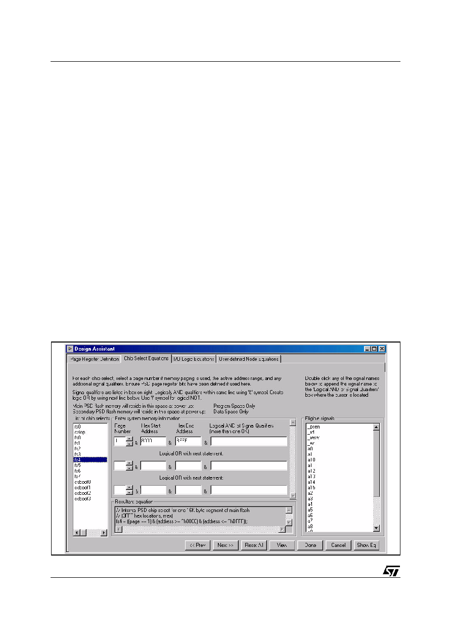
uPSD34xx - PSD MODULE
170/264
Specifying the Memory Map with PSDsoft Ex-
press. The memory map example shown in
Fig-
ure 64., page 169
is implemented using PSDsoft
Express in a point-and-click environment. PSDsoft
Express will automatically generate Hardware
Definition Language (HDL) statements of the
ABEL language for the DPLD, such as those
shown in Table
103
.
Specifying these equations using PSDsoft Ex-
press is very simple. For example, Figure
65
, page
84 shows how to specify the chip-select equation
for the 16K byte Flash memory segment, fs4. No-
tice fs4 is on memory page 1. This specification
process is repeated for all other Flash memory
segments, the SRAM, the csiop register block, and
any external chip select signals that may be need-
ed.
Table 103. HDL Statement Example Generated from PSDsoft Express for Memory Map
Figure 65. PSDsoft Express Memory Mapping
rs0 = ((address
^h0000) & (address ^h1FFF));
csiop = ((address
^h2000) & (address ^h20FF));
fs0 = ((address
^h0000) & (address ^h3FFF));
fs1 = ((address
^h4000) & (address ^h7FFF));
fs2 = ((page == 0)
& (address
^h8000) & (address ^hBFFF));
fs3 = ((page == 0)
& (address
^hC000) & (address ^hFFFF));
fs4 = ((page == 1)
& (address
^h8000) & (address ^hBFFF));
fs5 = ((page == 1)
& (address
^hC000) & (address ^hFFFF));
fs6 = ((page == 2)
& (address
^h8000) & (address ^hBFFF));
fs7 = ((page == 2)
& (address
^hC000) & (address ^hFFFF));
csboot0 = ((address
^h8000) & (address ^h9FFF));
csboot1 = ((address
^hA000) & (address ^hBFFF));
csboot2 = ((address
^hC000) & (address ^hDFFF));
csboot3 = ((address
^hE000) & (address ^hFFFF));

171/264
uPSD34xx - PSD MODULE
EEPROM Emulation. EEPROM emulation is
needed if it is desired to repeatedly change only a
small number of bytes of data in Flash memory. In
this case EEPROM emulation is needed because
although Flash memory can be written byte-by-
byte, it must be erased sector-by-sector, it is not
erasable byte-by-byte (unlike EEPROM which is
written AND erased byte-by-byte). So changing
one or two bytes in Flash memory typically re-
quires erasing an entire sector each time only one
byte is changed within that sector.
However, two of the 8K byte sectors of Secondary
Flash memory may be used to emulate EEPROM
by using a linked-list software technique to create
a small data set that is maintained by alternating
between the two flash sectors. For example, a
data set of 128 bytes is written and maintained by
software in a distributed fashion across one 8K
byte sector of Secondary Flash memory until it be-
comes full. Then the writing continues on the other
8K byte sector while erasing the first 8K byte sec-
tor. This process repeats continuously, bouncing
back and forth between the two 8K byte sectors.
This creates a wear-leveling effect, which increas-
es the effective number of erase cycles for a data
set of 128 bytes to many times more than the base
100K erase cycles of the Flash memory. EEPROM
emulation in Flash memory is typically faster than
writing to actual EEPROM memory, and more reli-
able because the last known value in a data set is
maintained even if a WRITE cycle is corrupted by
a power outage. The EEPROM emulation function
can be called by the user's firmware, making it ap-
pear that the user is writing a single byte, or data
record, thus hiding all of the data management
that occurs within the two 8K byte flash sectors.
EEPROM emulation firmware for the uPSD34xx is
available from www.st.com/psm.
Alternative Mapping Schemes. Here are more
possible memory maps for the uPSD3433.
Note: Mapping examples would be slightly differ-
ent for uPSD3433 and uPSD3434, because of the
different sizes of individual Flash memory sectors.
≠
Figure 66.
Place the larger Main Flash
Memory into program space, but split the
Secondary Flash in half, placing two of its
sectors into XDATA space and remaining two
sectors into program space. This method
allows the designer to put IAP code (or boot
code) into two sectors of Secondary Flash in
program space, and use the other two
Secondary Flash sectors for data storage,
such as EEPROM emulation in XDATA space.
≠
Figure 67.
Place both the Main and
Secondary Flash memories into program
space for maximum code storage, with no
Flash memory in XDATA space.
Figure 66. Mapping: Split Second Flash in Half
Figure 67. Mapping: All Flash in Code Space
0000h
8000h
4000h
6000h
FFFFh
8032 XDATA SPACE
(RD and WR)
8032 PROGRAM
SPACE (PSEN)
csboot1, 8KB
Common Memory to All Pages
csboot0, 8KB
Common Memory to All Pages
csboot2
8KB
csboot3
8KB
Page X
rs0, 8KB
csiop, 256B
fs7
16KB
fs3
16KB
fs1
16KB
Page
0
Page
1
Page
2
Page
3
2000h
0000h
8000h
FFFFh
Nothing Mapped
fs6
16KB
fs5
16KB
fs4
16KB
fs2
16KB
fs0
16KB
System I/O
System I/O
C000h
2100h
4000h
2000h
AI09174
0000h
8000h
4000h
6000h
FFFFh
8032 XDATA SPACE
(RD and WR)
8032 PROGRAM
SPACE (PSEN)
csboot1, 8KB
Common Memory to All Pages
csboot0, 8KB
Common Memory to All Pages
csboot2, 8KB
Common Memory to All Pages
csboot3, 8KB
Common Memory to All Pages
Page X
rs0, 8KB
csiop, 256B
fs7
16KB
fs3
16KB
fs1
16KB
Page
0
Page
1
Page
2
Page
3
2000h
0000h
FFFFh
fs6
16KB
fs5
16KB
fs4
16KB
fs2
16KB
fs0
16KB
System I/O
C000h
2100h
2000h
AI09175
uPSD34xx - PSD MODULE
172/264
≠
Figure 68.
Place the larger Main Flash
Memory into XDATA space and the smaller
Secondary Flash into program space for
systems that need a large amount of Flash for
data recording or large look-up tables, and not
so much Flash for 8032 firmware.
Figure 68. Mapping: Small Code / Big Data
It is also possible to "reclassify" the Flash memo-
ries during runtime, moving the memories be-
tween XDATA memory space and program
memory space on-the-fly. This essentially means
that the user can override the initial setting during
run-time by writing to a csiop register (the VM Reg-
ister). This is useful for IAP, because standard
8051 architecture does not allow writing to pro-
gram space. For example, if the user wants to up-
date firmware in Main Flash memory that is
residing in program space, the user can temporari-
ly "reclassify" the Main Flash memory into XDATA
space to erase and rewrite it while executing IAP
code from the Secondary Flash memory in pro-
gram space. After the writing is complete, the Main
Flash can be "reclassified" back to program space,
then execution can continue from the new code in
Main Flash memory. The mapping example of Fig-
ure
68
will accommodate this operation.
Memory Sector Select Rules. When defining
sector select signals (FSx, CSBOOTx, RS0,
CSIOP, PSELx) in PSDsoft Express, the user
must keep these rules in mind:
≠
Main Flash and Secondary Flash memory
sector select signals may not be larger than
their physical sector size as defined in
Table
101., page 166
.
≠
Any Main Flash memory sector select may not
be mapped in the same address range as
another Main Flash sector select (cannot
overlap segments of Main Flash on top of
each other).
≠
Any Secondary Flash memory sector select
may not be mapped in the same address
range as another Secondary Flash sector
select (cannot overlap segments of
Secondary Flash on top of each other).
≠
A Secondary Flash memory sector may
overlap a Main Flash memory sector. In the
case of overlap, priority is given to the
Secondary Flash memory sector.
≠
SRAM, CSIOP, or PSELx may overlap any
Flash memory sector. In the case of overlap,
priority is given to SRAM, CSIOP, or PSELx.
Note: PSELx is for optional Peripheral I/O
Mode on Port A.
≠
The address range for sector selects for
SRAM, PSELx, and CSIOP must not overlap
each other as they have the same priority,
causing contention if overlapped.
0000h
8000h
4000h
6000h
FFFFh
8032 XDATA SPACE
(RD and WR)
8032 PROGRAM
SPACE (PSEN)
csboot0
8KB
csboot1
8KB
csboot2
8KB
csboot3
8KB
Page X
rs0, 8KB
Common Memory to All Pages
csiop, 256 bytes,
Common to All Pages
fs7
16KB
fs3
16KB
fs1
16KB
Page
0
Page
1
Page
2
Page
3
2000h
0000h
8000h
FFFFh
Nothing
Mapped
fs6
16KB
fs5
16KB
fs4
16KB
fs2
16KB
fs0
16KB
System I/O
C000h
2100h
2000h
AI09176
173/264
uPSD34xx - PSD MODULE
Figure
69
illustrates the priority scheme of the
memory elements of the PSD Module. Priority re-
fers to which memory will ultimately produce a
byte of data or code to the 8032 MCU for a given
bus cycle. Any memory on a higher level can over-
lap and has priority over any memory on a lower
level. Memories on the same level must not over-
lap.
Example: FS0 is valid when the 8032 produces an
address in the range of 8000h to BFFFh.
CSBOOT0 is valid from 8000h to 9FFFh. RS0 is
valid from 8000h to 87FFh. Any address from the
8032 in the range of RS0 always accesses the
SRAM. Any address in the range of CSBOOT0
greater than 87FFh (and less than 9FFFh) auto-
matically addresses Secondary Flash memory.
Any address greater than 9FFFh accesses Main
Flash memory. One-half of the Main Flash memo-
ry segment and one-fourth of the Secondary Flash
memory segment cannot be accessed by the
8032.
Figure 69. PSD Module Memory Priority
The VM Register. One of the csiop registers (the
VM Register) controls whether or not the 8032 bus
control signals RD, WR, and PSEN are routed to
the Main Flash memory, or the Secondary Flash
memory. Routing of these signals to these PSM
Module memories determines if memories reside
in 8032 program address space, 8032 XDATA
space, or both. The initial setting of the VM Regis-
ter is determined by a choice in PSDsoft Express
and programmed into the uPSD34xx in a non-vol-
atile fashion using JTAG. This initial setting is
loaded into the VM Register upon power-up and
also loaded upon any reset event. However, the
8032 may override the initial VM Register setting
at run-time by writing to the VM Register, which is
useful for IAP.
Table 104., page 174
defines bit functions within
the VM Register.
Note: Bit 7, PIO_EN, is not related to the memory
manipulation functions of Bits 1, 2, 3, and 4. SRAM
and csiop registers are always in XDATA space
and cannot reside in program space.
Figure 70., page 174
illustrates how the VM Reg-
ister affects the routing of RD, WR, and PSEN to
the memories on the PSD Module. As an example,
if we apply the value 0Ch to the VM Register to im-
plement the memory map example shown in
Fig-
ure 64., page 169
, then the routing of RD, WR,
and PSEN would look like that shown in
Figure
71., page 175
.
In this example, the configuration is specified in
PSDsoft Express and programmed into the
uPSD34xx using JTAG. Upon power-on or any re-
set condition, the non-volatile value 0Ch is loaded
into the VM Register. At runtime, the value 0Ch in
the VM Register may be changed (overridden) by
the 8032 if desired to implement IAP or other func-
tions.
Level 1
SRAM,
CSIOP, and
Peripheral I/O
Mode
Highest Priority
Level 2
Secondary
Flash Memory
Level 3
Main Flash Memory
Lowest Priority
AI02867E
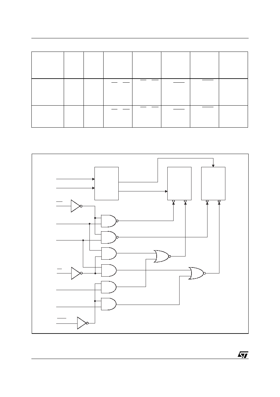
uPSD34xx - PSD MODULE
174/264
Table 104. VM Register (address = csiop + offset E2h)
Note: 1. Default value of Bits 1, 2, 3, and 4 is loaded from Non-Volatile setting as specified from PSDsoft Express upon any reset or power-
up condition. The default value of these bits can be overridden by 8032 at run-time.
2. Default value of Bit 7 is zero upon any reset condition.
Figure 70. VM Register Control of Memories
Bit 7
PIO_EN
Bit 6
Bit 5
Bit 4
Main Flash
XDATA
Space
Bit 3
Secondary
Flash XDATA
Space
Bit 2
Main Flash
Program
Space
Bit 1
Secondary
Flash
Program
Space
Bit 0
0 = disable
Peripheral I/O
Mode on Port A
not used
not used
0 = RD or WR
cannot
access Main
Flash
0 = RD or WR
cannot
access
Secondary
Flash
0 = PSEN
cannot
access Main
Flash
0 = PSEN
cannot
access
Secondary
Flash
not used
1 = enable
Peripheral I/O
Mode on Port A
not used
not used
1 = RD or WR
can access
Main Flash
1 = RD or WR
can access
Secondary
Flash
1 = PSEN
can access
Main Flash
1 = PSEN
can access
Secondary
Flash
not used
DPLD
Main Flash
Memory
Secondary
Flash
Memory
CS
CS
FS0 - FS7
CSBOOT0 - CSBOOT3
WR
VM REG BIT 4
VM REG BIT 3
VM REG BIT 1
VM REG BIT 2
RD
WR
OE
WR
OE
8032 Address
53 Other PLD Inputs
PSEN
AI10455
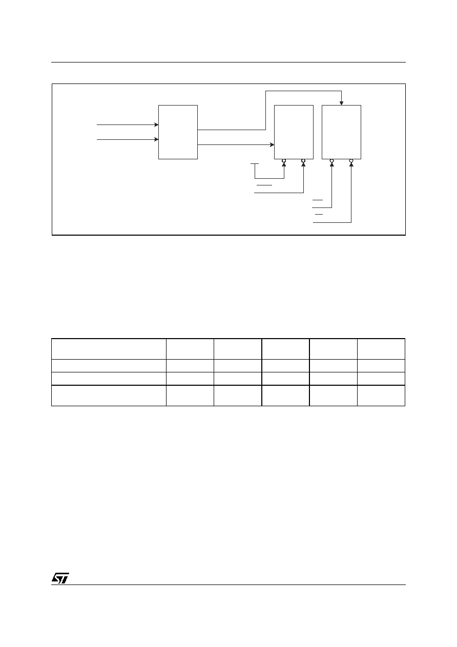
175/264
uPSD34xx - PSD MODULE
Figure 71. VM Register Example Corresponding to Memory Map Example
PSD Module Data Bus Width
The PSD Module functions as an 8-bit device to
the MCU Module except when the PFQ is fetching
instructions from the Flash memory. When PSEN
is active, the PSD Module always drives 16-bit
data out onto the bus.
The Flash memories are 16-bit wide when it is in
Program Memory space and are 8-bit wide when it
is in the Data Space. When the Flash memory is
configured in both "Program Space" and "Data
Space," the Flash will drive 16-bit in a PSEN cycle
and operates as an 8-bit memory in READ or
WRITE cycle.
The SRAM, csiop, and external device are always
in 8-bit data space.
Table 105. Data Width in Different Bus Cycles
Note: x = NA
DPLD
Main Flash
Memory
Secondary
Flash
Memory
CS
CS
FS0 - FS7
CSBOOT0 - CSBOOT3
WR
OE
WR
OE
8032 Address
53 Other PLD Inputs
WR
PSEN
RD
VM Register = 0Ch
AI10456
Type of Bus Cycle
Main Flash
Secondary
Flash
SRAM
CSIOP
External
Device
PSEN Cycle (Program Memory)
16-bit
16-bit
x
x
x
Read or Write Cycle (Data Memory)
8-bit
8-bit
8-bit
8-bit
8-bit
Flash Programming Cycle (Flash
Write or Reading Status)
8-bit
8-bit
x
x
x

uPSD34xx - PSD MODULE
176/264
Runtime Control Register Definitions (csiop)
The 39 csiop registers are defined in Table
106
.
The 8032 can access each register by the address
offset (specified in Table
106
) added to the csiop
base address that was specified in PSDsoft Ex-
press. Do not write to unused locations within the
csiop block of 256 registers, they should remain
logic zero.
Table 106. CSIOP Registers and their Offsets (in hexadecimal)
Register
Name
Port A
(80-pin)
Port B
Port C
Port D
Other
Description
Link
Data
In
00h
01h 10h 11h
MCU I/O input mode. Read to obtain
current logic level of pins on Ports A, B,
C, or D. No WRITEs.
Table
122., page
203
Control
02h
03h
Selects MCUI/O or Latched Address
Out mode. Logic 0 = MCU I/O, 1 = 8032
Addr Out. Write to select mode. Read for
status.
Table
134., page
208
Data
Out
04h
05h 12h 13h
MCU I/O output mode. Write to set logic
level on pins of Ports A, B, C, or D. Read
to check status. This register has no
effect if a port pin is driven by an OMC
output from PLD.
Table
126., page
203
Direction
06h
07h 14h 15h
MCU I/O mode. Configures port pin as
input or output. Write to set direction of
port pins.
Logic 1 = out, Logic 0 = in. Read to
check status.
Table
130., page
204
Drive
Select 08h
09h 16h 17h
Write to configure port pins as either
CMOS push-pull or Open Drain on some
pins, while selecting high slew rate on
other pins. Read to check status. Default
output type is CMOS push-pull.
Table
136., page
210
Input
Macrocells
0Ah
0Bh 18h
Read to obtain logic state of IMCs. No
WRITEs.
Table
117., page
198
Enable Out
OCh
0Dh
1Ah
1Bh
Read state of output enable logic on
each I/O port driver. 1 = driver output is
enabled, 0 = driver is off, and it is in high
impedance state. No WRITEs.
Table
140., page
211
Output
Macrocells AB
(MCELLAB)
20h
Read logic state of MCELLAB outputs
(bank of eight OMCs).
Write to load MCELLAB flip-flops.
Table
113., page
196
Output
Macrocells BC
(MCELLBC)
21h
Read logic state of MCELLBC outputs
(bank of eight OMCs).
Write to load MCELLBC flip-flops.
Table
114., page
196
Mask
Macrocells AB
22h
Write to set mask for MCELLAB. Logic
'1' blocks READs/WRITEs of OMC.
Logic '0' will pass OMC value. Read to
check status.
Table
115., page
197
Mask
Macrocells BC
23h
Write to set mask for MCELLBC. Logic
'1' blocks READs/WRITEs of OMC.
Logic '0' will pass OMC value. Read to
check status.
Table
116., page
197

177/264
uPSD34xx - PSD MODULE
Main Flash
Sector
Protection
C0h
Read to determine Main Flash Sector
Protection Setting (non-volatile) that was
specified in PSDsoft Express. No
WRITEs.
Table
109., page
186
Security Bit
and Secondary
Flash Sector
Protection
C2h
Read to determine if PSD Module
device Security Bit is active (non-
volatile) Logic 1 = device secured. Also
read to determine Secondary Flash
Protection Setting (non-volatile) that was
specified in PSDsoft. No WRITEs.
Table
110., page
186
PMMR0
B0h
Power Management Register 0. WRITE
and READ.
Table
144., page
219
PMMR2
B4h
Power Management Register 2. WRITE
and READ.
Table
145., page
219
PMMR3
C7h
Power Management Register 3. WRITE
and READ. However, Bit 1 can be
cleared only by a reset condition.
Table
146., page
219
Page
E0h
Memory Page Register. WRITE and
READ.
Figure
63., page
166
VM (Virtual
Memory)
E2h
Places PSD Module memories into 8032
Program Address Space and/or 8032
XDATA Address Space. (VM overrides
initial non-volatile setting that was
specified in PSDsoft Express. Reset
restores initial setting)
Table
104., page
174
Register
Name
Port A
(80-pin)
Port B
Port C
Port D
Other
Description
Link

uPSD34xx - PSD MODULE
178/264
PSD Module Detailed Operation
Specific details are given here for the following key
functional areas on the PSD Module:
Flash Memories
PLDs (DPLD and GPLD)
I/O Ports
Power Management
JTAG ISP and Debug Interface
Flash Memory Operation. The Flash memories
are accessed through the 8032 Address, Data,
and Control Bus interfaces. Flash memories (and
SRAM) cannot be accessed by any other bus
master other than the 8032 MCU (these are not
dual-port memories).
The 8032 cannot write to Flash memory as it
would an SRAM (supply address, supply data,
supply WR strobe, assume the data was correctly
written to memory). Flash memory must first be
"unlocked" with a special instruction sequence of
byte WRITE operations to invoke an internal algo-
rithm inside either Flash memory array, then a sin-
gle data byte is written (programmed) to the Flash
memory array, then programming status is
checked by a byte READ operation or by checking
the Ready/Busy pin (PC3).
Table 107., page 179
lists all of the special instruction sequences to pro-
gram a byte to either of the Flash memory arrays,
erase the arrays, and check for different types of
status from the arrays.
This unlocking sequence is typical for many Flash
memories to prevent accidental WRITEs by errant
code. However, it is possible to bypass this un-
locking sequence to save time while intentionally
programming Flash memory.
IMPORTANT: The 8032 may not read and exe-
cute code from the same Flash memory array for
which it is directing an instruction sequence. Or
more simply stated, the 8032 may not read code
from the same Flash array that is writing or eras-
ing. Instead, the 8032 must execute code from an
alternate memory (like SRAM or a different Flash
array) while sending instruction sequences to a
given Flash array. Since the two Flash memory ar-
rays inside the PSD Module device are completely
independent, the 8032 may read code from one
array while sending instructions to the other. It is
possible, however, to suspend a sector erase op-
eration in one particular Flash array in order to ac-
cess a different sector within that same Flash
array, then resume the erase later.
After a Flash memory array is programmed or
erased it will go to "Read Array" mode, then the
8032 can read from Flash memory just as it would
read from any ROM or SRAM device.
Flash Memory Instruction Sequences. An in-
struction sequence consists of a sequence of spe-
cific byte WRITE and byte READ operations. Each
byte written to either Flash memory array on the
PSD Module is received by a state machine inside
the Flash array and sequentially decoded to exe-
cute an embedded algorithm. The algorithm is ex-
ecuted when the correct number of bytes are
properly received and the time between two con-
secutive bytes is shorter than the time-out period
of 80µs. Some instruction sequences are struc-
tured to include READ operations after the initial
WRITE operations.
An instruction sequence must be followed exactly.
Any invalid combination of instruction bytes or
time-out between two consecutive bytes while ad-
dressing Flash memory resets the PSD Module
Flash logic into Read Array mode (where Flash
memory is read like a ROM device). The Flash
memories support instruction sequences summa-
rized in
Table 107., page 179
.
Program a Byte
Unlock Sequence Bypass
Erase memory by array or by sector
Suspend or resume a sector erase
Reset to Read Array mode
The first two bytes of an instruction sequence are
8032 bus WRITE operations to "unlock" the Flash
array, followed by writing a command byte. The
bus operations consist of writing the data AAh to
address X555h during the first bus cycle and data
55h to address XAAAh during the second bus cy-
cle. 8032 address signals A12-A15 are "Don't
care" during the instruction sequence during
WRITE cycles. However, the appropriate sector
select signal (FSx or CSBOOTx) from the DPLD
must be active during the entire instruction se-
quence to complete the entire 8032 address (this
includes the page number when memory paging is
used). Ignoring A12-A15 means the user has more
flexibility in memory mapping. For example, in
many traditional Flash memories, instruction se-
quences must be written to addresses AAAAh and
5555h, not XAAAh and X555h like supported on
the PSD Module. When the user has to write to
AAAAh and 5555h, the memory mapping options
are limited.
The Main Flash and Secondary Flash memories
each have the same instruction set shown in
Table
107., page 179
, but the sector select signals de-
termine which memory array will receive and exe-
cute the instructions.

179/264
uPSD34xx - PSD MODULE
Table 107. Flash Memory Instruction Sequences
(1,2)
Instr.
Sequence
Bus
Cycle 1
Bus
Cycle 2
Bus
Cycle 3
Bus
Cycle 4
Bus
Cycle 5
Bus
Cycle 6
Bus
Cycle 7
Link
Read
Memory
Contents
(Read
Array
mode)
Read byte
from any
valid Flash
memory addr
Read Memory
Contents., pa
ge 180
Program
(write) a
Byte to
Flash
Memory
Write AAh to
X555h
(unlock)
Write 55h
to XAAAh
(unlock)
Write A0h
to X555h
(command)
Write data
byte to
address
Programming
Flash
Memory., pag
e 181
Bypass
Unlock
Write AAh to
X555h
(unlock)
Write 55h
to XAAAh
(unlock)
Write 20h
to X555h
(command)
Bypassed
Unlock
Sequence, pa
ge 184
Program a
Byte to
Flash
Memory
with
Bypassed
Unlock
Write A0h to
XXXXh
(command)
Write data
byte to
address
Bypassed
Unlock
Sequence, pa
ge 184
Reset
Bypass
Unlock
Write 90h to
XXXXh
(command)
Write 00h
to XXXXh
(command)
Bypassed
Unlock
Sequence, pa
ge 184
Flash Bulk
Erase
(3)
Write AAh to
X555h
(unlock)
Write 55h
to XAAAh
(unlock)
Write 80h
to X555h
(command)
Write AAh
to X555h
(unlock)
Write 55h
to XAAAh
(unlock)
Write 10h to
X555h
(command)
Flash Bulk
Erase., page
184
Flash
Sector
Erase
Write AAh to
X555h
(unlock)
Write 55h
to XAAAh
(unlock)
Write 80h
to X555h
(command)
Write AAh
to X555h
(unlock)
Write 55h
to XAAAh
(unlock)
Write 30h to
desired
Sector
(command)
Write 30h
to
another
Sector
(command)
Flash Sector
Erase., page
185
Suspend
Sector
Erase
Write B0h to
address that
activates FSx
or CSBOOTx
where erase
is in progress
(command)
Suspend
Sector
Erase., page
185
Resume
Sector
Erase
Write 30h to
address that
activates FSx
or CSBOOTx
where
desired to
resume
erase
(command)
Resume
Sector
Erase., page
185

uPSD34xx - PSD MODULE
180/264
Note: 1. All values are in hexadecimal, X = Don't care
2. 8032 addresses A12 through A15 are "Don't care" during the instruction sequence decoding. Only address bits A0-A11 are used
during decoding of Flash memory instruction sequences. The individual sector select signal (FS0 - FS7 or CSBOOT0-CSBOOT3)
which is active during the instruction sequence determines the complete address.
3. Directing this command to any individual sector within a Flash memory array will invoke the bulk erase of all Flash memory sectors
within that array.
Reading Flash Memory. Under typical condi-
tions, the 8032 may read the Flash memory using
READ operations (READ bus cycles) just as it
would a ROM or RAM device. Alternately, the
8032 may use READ operations to obtain status
information about a Program or Erase operation
that is currently in progress. The following sections
describe the kinds of READ operations.
Read Memory Contents. Flash memory is
placed in the Read Array mode after Power-up, af-
ter a PSD Module reset event, or after receiving a
Reset Flash memory instruction sequence from
the 8032. The 8032 can read Flash memory con-
tents using standard READ bus cycles anytime the
Flash array is in Read Array mode. Flash memo-
ries will always be in Read Array mode when the
array is not actively engaged in a program or erase
operation.
Reading the Erase/Program Status Bits. The
Flash arrays provide several status bits to be used
by the 8032 to confirm the completion of an erase
or program operation on Flash memory, shown in
Table 108., page 181
. The status bits can be read
as many times as needed until an operation is
complete.
The 8032 performs a READ operation to obtain
these status bits while an erase or program oper-
ation is being executed by the state machine in-
side each Flash memory array.
Data Polling Flag (DQ7). While programming ei-
ther Flash memory, the 8032 may read the Data
Polling Flag Bit (DQ7), which outputs the comple-
ment of the D7 Bit of the byte being programmed
into Flash memory. Once the program operation is
complete, DQ7 is equal to D7 of the byte just pro-
grammed into Flash memory, indicating the pro-
gram cycle has completed successfully. The
correct select signal, FSx or CSBOOTx, must be
active during the entire polling procedure.
Polling may also be used to indicate when an
erase operation has completed. During an erase
operation, DQ7 is '0.' After the erase is complete
DQ7 is '1.' The correct select signal, FSx or CS-
BOOTx, must be active during the entire polling
procedure.
DQ7 is valid after the fourth instruction byte
WRITE operation (for program instruction se-
quence) or after the sixth instruction byte WRITE
operation (for erase instruction sequence).
If all Flash memory sectors to be erased are pro-
tected, DQ7 is reset to '0' for about 100µs, and
then DQ7 returns to the value of D7 of the previ-
ously addressed byte. No erasure is performed.
Toggle Flag (DQ6). The Flash memories offer an
alternate way to determine when a Flash memory
program operation has completed. During the pro-
gram operation and while the correct sector select
FSx or CSBOOTx is active, the Toggle Flag Bit
(DQ6) toggles from '0' to '1' and '1' to '0' on subse-
quent attempts to read any byte of the same Flash
array.
When the internal program operation is complete,
the toggling stops and the data read on the data
bus D0-7 is the actual value of the addressed
memory byte. The device is now accessible for a
new READ or WRITE operation. The operation is
finished when two successive READs yield the
same value for DQ6.
DQ6 may also be used to indicate when an erase
operation has completed. During an erase opera-
tion, DQ6 will toggle from '0' to '1' and '1' to '0' until
the erase operation is complete, then DQ6 stops
toggling. The erase is finished when two succes-
sive READs yield the same value of DQ6. The cor-
rect sector select signal, FSx or CSBOOTx, must
be active during the entire procedure.
DQ6 is valid after the fourth instruction byte
WRITE operation (for program instruction se-
quence) or after the sixth instruction byte WRITE
operation (for erase instruction sequence).
If all the Flash memory sectors selected for era-
sure are protected, DQ6 toggles to '0' for about
100µs, then returns value of D6 of the previously
addressed byte.
Reset
Flash
Write F0h to
address that
activates FSx
or CSBOOTx
in desired
array.
(command)
Reset
Flash, page 1
85
Instr.
Sequence
Bus
Cycle 1
Bus
Cycle 2
Bus
Cycle 3
Bus
Cycle 4
Bus
Cycle 5
Bus
Cycle 6
Bus
Cycle 7
Link

181/264
uPSD34xx - PSD MODULE
Error Flag (DQ5). During a normal program or
erase operation, the Error Flag Bit (DQ5) is to '0'.
This bit is set to '1' when there is a failure during
Flash memory byte program, sector erase, or bulk
erase operations.
In the case of Flash memory programming, DQ5
Bit indicates an attempt to program a Flash mem-
ory bit from the programmed state of '0,' to the
erased state of 1, which is not valid. DQ5 may also
indicate a particular Flash cell is damaged and
cannot be programmed.
In case of an error in a Flash memory sector erase
or byte program operation, the Flash memory sec-
tor in which the error occurred or to which the pro-
grammed byte belongs must no longer be used.
Other Flash memory sectors may still be used.
DQ5 is reset after a Reset Flash instruction se-
quence.
Erase Time-out Flag (DQ3). The Erase Time-
out Flag Bit (DQ3) reflects the time-out period al-
lowed between two consecutive sector erase in-
struction sequence bytes. If multiple sector erase
commands are desired, the additional sector
erase commands (30h) must be sent by the 8032
within 80us after the previous sector erase com-
mand. DQ3 is 0 before this time period has ex-
pired, indicating it is OK to issue additional sector
erase commands. DQ3 will go to logic '1' if the time
has been longer than 80µs since the previous sec-
tor erase command (time has expired), indication
that is not OK to send another sector erase com-
mand. In this case, the 8032 must start a new sec-
tor erase instruction sequence (unlock and
command) beginning again after the current sec-
tor erase operation has completed.
Programming Flash Memory. When a byte of
Flash memory is programmed, individual bits are
programmed to logic '0.' cannot program a bit in
Flash memory to a logic '1' once it has been pro-
grammed to a logic '0.' A bit must be erased to log-
ic '1', and programmed to logic '0.' That means
Flash memory must be erased prior to being pro-
grammed. A byte of Flash memory is erased to all
1s (FFh). The 8032 may erase the entire Flash
memory array all at once, or erase individual sec-
tor-by-sector, but not erase byte-by-byte. Howev-
er, even though the Flash memories cannot be
erased byte-by-byte, the 8032 may program Flash
memory byte-by-byte. This means the 8032 does
not need to program group of bytes (64, 128, etc.)
at one time, like some Flash memories.
Each Flash memory requires the 8032 to send an
instruction sequence to program a byte or to erase
sectors (see
Table 107., page 179
).
If the byte to be programmed is in a protected
Flash memory sector, the instruction sequence is
ignored.
IMPORTANT: It is mandatory that a chip-select
signal is active for the Flash sector where a pro-
gramming instruction sequence is targeted. The
user must make sure that the correct chip-select
equation, FSx or CSBOOTx specified in PSDsoft
Express matches the address range that the 8032
firmware is accessing, otherwise the instruction
sequence will not be recognized by the Flash ar-
ray. If memory paging is used, be sure that the
8032 firmware sets the page register to the correct
page number before issuing an instruction se-
quence to the Flash memory segment on a partic-
ular memory page, otherwise the correct sector
select signal will not become active.
Once the 8032 issues a Flash memory program or
erase instruction sequence, it must check the sta-
tus bits for completion. The embedded algorithms
that are invoked inside a Flash memory array pro-
vide several ways to give status to the 8032. Sta-
tus may be checked using any of three methods:
Data Polling, Data Toggle, or Ready/Busy (pin
PC3).
Table 108. Flash Memory Status Bit Definition
Note: 1. X = Not guaranteed value, can be read either '1' or '0.'
2. DQ7-DQ0 represent the 8032 Data Bus Bits, D7-D0.
Functional Block
FSx, or CSBOOTx
DQ7
DQ6
DQ5
DQ4
DQ3
DQ2
DQ1
DQ0
Flash Memory
Active (the desired
segment is selected)
Data
Polling
Toggle
Flag
Error
Flag
X
Erase
Time-
out
X
X
X

uPSD34xx - PSD MODULE
182/264
Data Polling. Polling on the Data Polling Flag Bit
(DQ7) is a method of checking whether a program
or erase operation is in progress or has complet-
ed. Figure
72
shows the Data Polling algorithm.
When the 8032 issues a program instruction se-
quence, the embedded algorithm within the Flash
memory array begins. The 8032 then reads the lo-
cation of the byte to be programmed in Flash
memory to check status. The Data Polling Flag Bit
(DQ7) of this location becomes the compliment of
Bit D7 of the original data byte to be programmed.
The 8032 continues to poll this location, compar-
ing the Data Polling Flag Bit (DQ7) and monitoring
the Error Flag Bit (DQ5). When the Data Polling
Flag Bit (DQ7) matches Bit D7 of the original data,
then the embedded algorithm is complete. If the
Error Flag Bit (DQ5) is '1,' the 8032 should test the
Data Polling Flag Bit (DQ7) again since the Data
Polling Flag Bit (DQ7) may have changed simulta-
neously with the Error Flag Bit (DQ5) (see Figure
72
).
The Error Flag Bit (DQ5) is set if either an internal
time-out occurred while the embedded algorithm
attempted to program the byte (indicating a bad
Flash cell) or if the 8032 attempted to program bit
to logic '1' when that bit was already programmed
to logic '0' (must erase to achieve logic '1').
It is suggested (as with all Flash memories) to read
the location again after the embedded program-
ming algorithm has completed, to compare the
byte that was written to the Flash memory with the
byte that was intended to be written.
When using the Data Polling method during an
erase operation, Figure
72
still applies. However,
the Data Polling Flag Bit (DQ7) is '0' until the erase
operation is complete. A '1' on the Error Flag Bit
(DQ5) indicates a time-out condition on the Erase
cycle, a '0' indicates no error. The 8032 can read
any location within the sector being erased to get
the Data Polling Flag Bit (DQ7) and the Error Flag
Bit (DQ5).
PSDsoft Express generates ANSI C code func-
tions the user may use to implement these Data
Polling algorithms.
Figure 72. Data Polling Flowchart
READ DQ5 & DQ7
at VALID ADDRESS
START
READ DQ7
FAIL
PASS
AI01369B
DQ7
=
DATA
YES
NO
YES
NO
DQ5
= 1
DQ7
=
DATA
YES
NO
183/264
uPSD34xx - PSD MODULE
Data Toggle. Checking the Toggle Flag Bit
(DQ6) is another method of determining whether a
program or erase operation is in progress or has
completed. Figure
73
shows the Data Toggle algo-
rithm.
When the 8032 issues a program instruction se-
quence, the embedded algorithm within the Flash
memory array begins. The 8032 then reads the lo-
cation of the byte to be programmed in Flash
memory to check status. The Toggle Flag Bit
(DQ6) of this location toggles each time the 8032
reads this location until the embedded algorithm is
complete. The 8032 continues to read this loca-
tion, checking the Toggle Flag Bit (DQ6) and mon-
itoring the Error Flag Bit (DQ5). When the Toggle
Flag Bit (DQ6) stops toggling (two consecutive
reads yield the same value), then the embedded
algorithm is complete. If the Error Flag Bit (DQ5) is
'1,' the 8032 should test the Toggle Flag Bit (DQ6)
again, since the Toggle Flag Bit (DQ6) may have
changed simultaneously with the Error Flag Bit
(DQ5) (see Figure
73
).
The Error Flag Bit (DQ5) is set if either an internal
time-out occurred while the embedded algorithm
attempted to program the byte, or if the 8032 at-
tempted to program bit to logic '1' when that bit
was already programmed to logic '0' (must erase
to achieve logic '1').
It is suggested (as with all Flash memories) to read
the location again after the embedded program-
ming algorithm has completed, to compare the
byte that was written to Flash memory with the
byte that was intended to be written.
When using the Data Toggle method during an
erase operation, Figure
73
still applies. the Toggle
Flag Bit (DQ6) toggles until the erase operation is
complete. A '1' on the Error Flag Bit (DQ5) indi-
cates a time-out condition on the Erase cycle, a '0'
indicates no error. The 8032 can read any location
within the sector being erased to get the Toggle
Flag Bit (DQ6) and the Error Flag Bit (DQ5).
PSDsoft Express generates ANSI C code func-
tions the user may use to implement these Data
Toggling algorithms.
Figure 73. Data Toggle Flowchart
READ
DQ5 & DQ6
START
READ DQ6
FAIL
PASS
AI01370B
DQ6
=
TOGGLE
NO
NO
YES
YES
DQ5
= 1
NO
YES
DQ6
=
TOGGLE

uPSD34xx - PSD MODULE
184/264
Ready/Busy (PC3). This signal can be used to
output the Ready/Busy status of a program or
erase operation on either Flash memory. The out-
put on the Ready/Busy pin is a '0' (Busy) when ei-
ther Flash memory array is being written, or when
either Flash memory array is being erased. The
output is a '1' (Ready) when no program or erase
operation is in progress. To activate this function
on this pin, the user must select the "Ready/Busy"
selection in PSDsoft Express when configuring pin
PC3. This pin may be polled by the 8032 or used
as a 8032 interrupt to indicate when an erase or
program operation is complete (requires routing
the signal on PC board from PC3 back into a pin
on the MCU Module). This signal is also available
internally on the PSD Module as an input to both
PLDs (without routing a signal externally on PC
board) and its signal name is "rd_bsy". The Ready/
Busy output can be probed during lab develop-
ment to check the timing of Flash memory pro-
gramming in the system at run-time.
Bypassed Unlock Sequence. The Bypass Un-
lock mode allows the 8032 to program bytes in the
Flash memories faster than using the standard
Flash program instruction sequences because the
typical AAh, 55h unlock bus cycles are bypassed
for each byte that is programmed. Bypassing the
unlock sequence is typically used when the 8032
is intentionally programming a large number of
bytes (such as during IAP). After intentional pro-
gramming is complete, typically the Bypass mode
would be disabled, and full protection is back in
place to prevent unwanted WRITEs to Flash mem-
ory.
The Bypass Unlock mode is entered by first initiat-
ing two Unlock bus cycles. This is followed by a
third WRITE operation containing the Bypass Un-
lock command, 20h (as shown in
Table
107., page 179
). The Flash memory array that re-
ceived that sequence then enters the Bypass Un-
lock mode. After this, a two bus cycle program
operation is all that is required to program a byte
in this mode. The first bus cycle in this shortened
program instruction sequence contains the By-
passed Unlocked Program command, A0h, to any
valid address within the unlocked Flash array. The
second bus cycle contains the address and data of
the byte to be programmed. Programming status
is checked using toggle, polling, or Ready/Busy
just as before. Additional data bytes are pro-
grammed the same way until this Bypass Unlock
mode is exited.
To exit Bypass Unlock mode, the system must is-
sue the Reset Bypass Unlock instruction se-
quence. The first bus cycle of this instruction must
write 90h to any valid address within the unlocked
Flash Array; the second bus cycle must write 00h
to any valid address within the unlocked Flash Ar-
ray. After this sequence the Flash returns to Read
Array mode.
During Bypass Unlock Mode, only the Bypassed
Unlock Program instruction, or the Reset Bypass
Unlock instruction is valid, other instruction will be
ignored.
Erasing Flash Memory. Flash memory may be
erased sector-by-sector, or an entire Flash memo-
ry array may be erased with one command (bulk).
Flash Bulk Erase. The Flash Bulk Erase instruc-
tion sequence uses six WRITE operations fol-
lowed by a READ operation of the status register,
as described in
Table 107., page 179
. If any byte
of the Bulk Erase instruction sequence is wrong,
the Bulk Erase instruction sequence aborts and
the device is reset to the Read Array mode. The
address provided by the 8032 during the Flash
Bulk Erase command sequence may select any
one of the eight Flash memory sector select sig-
nals FSx or one of the four signals CSBOOTx. An
erase of the entire Flash memory array will occur
in a particular array even though a command was
sent to just one of the individual Flash memory
sectors within that array.
During a Bulk Erase, the memory status may be
checked by reading the Error Flag Bit (DQ5), the
Toggle Flag Bit (DQ6), and the Data Polling Flag
Bit (DQ7). The Error Flag Bit (DQ5) returns a '1' if
there has been an erase failure. Details of acquir-
ing the status of the Bulk Erase operation are de-
tailed in the section entitled "
Programming Flash
Memory., page 181
.
During a Bulk Erase operation, the Flash memory
does not accept any other Flash instruction se-
quences.

185/264
uPSD34xx - PSD MODULE
Flash Sector Erase. The Sector Erase instruc-
tion sequence uses six WRITE operations, as de-
scribed in
Table 107., page 179
. Additional Flash
Sector Erase commands to other sectors within
the same Flash array may be issued by the 8032
if the additional commands are sent within a limit-
ed amount of time.
The Erase Time-out Flag Bit (DQ3) reflects the
time-out period allowed between two consecutive
sector erase instruction sequence bytes. If multi-
ple sector erase commands are desired, the addi-
tional sector erase commands (30h) must be sent
by the 8032 to another sector within 80µs after the
previous sector erase command. DQ3 is 0 before
this time period has expired, indicating it is OK to
issue additional sector erase commands. DQ3 will
go to logic '1' if the time has been longer than 80µs
since the previous sector erase command (time
has expired), indicating that is not OK to send an-
other sector erase command. In this case, the
8032 must start a new sector erase instruction se-
quence (unlock and command), beginning again
after the current sector erase operation has com-
pleted.
During a Sector Erase operation, the memory sta-
tus may be checked by reading the Error Flag Bit
(DQ5), the Toggle Flag Bit (DQ6), and the Data
Polling Flag Bit (DQ7), as detailed in
Reading the
Erase/Program Status Bits, page 180
.
During a Sector Erase operation, a Flash memory
accepts only Reset Flash and Suspend Sector
Erase instruction sequences. Erasure of one
Flash memory sector may be suspended, in order
to read data from another Flash memory sector,
and then resumed.
The address provided with the initial Flash Sector
Erase command sequence (
Table
107., page 179
) must select the first desired sec-
tor (FSx or CSBOOTx) to erase. Subsequent sec-
tor erase commands that are appended within the
time-out period must be addressed to other de-
sired segments within the same Flash memory ar-
ray.
Suspend Sector Erase. When a Sector Erase
operation is in progress, the Suspend Sector
Erase instruction sequence can be used to sus-
pend the operation by writing B0h to any valid ad-
dress within the Flash array that currently is
undergoing an erase operation. This allows read-
ing of data from a different Flash memory sector
within the same array after the Erase operation
has been suspended. Suspend Sector Erase is
accepted only during an Erase operation.
There is up to 15µs delay after the Suspend Sector
Erase command is accepted and the array goes to
Read Array mode. The 8032 will monitor the Tog-
gle Flag Bit (DQ6) to determine when the erase
operation has halted and Read Array mode is ac-
tive.
If a Suspend Sector Erase instruction sequence
was executed, the following rules apply:
≠
Attempting to read from a Flash memory
sector that was being erased outputs invalid
data.
≠
Reading from a Flash memory sector that was
not being erased is valid.
≠
The Flash memory cannot be programmed,
and only responds to Resume Sector Erase
and Reset Flash instruction sequences.
≠
If a Reset Flash instruction sequence is
received, data in the Flash memory sector that
was being erased is invalid.
Resume Sector Erase. If a Suspend Sector
Erase instruction sequence was previously exe-
cuted, the erase cycle may be resumed with this
instruction sequence. The Resume Sector Erase
instruction sequence consists of writing the com-
mand 30h to any valid address within the Flash ar-
ray that was suspended as shown in
Table
107., page 179
.
Reset Flash. The Reset Flash instruction se-
quence resets the embedded algorithm running on
the state machine in the targeted Flash memory
(Main or Secondary) and the memory goes into
Read Array mode. The Reset Flash instruction
consists of one bus WRITE cycle as shown in
Ta-
ble 107., page 179
, and it must be executed after
any error condition that has occurred during a
Flash memory Program or Erase operation.
It may take the Flash memory up to 25µs to com-
plete the Reset cycle. The Reset Flash instruction
sequence is ignored when it is issued during a
Program or Bulk Erase operation. The Reset Flash
instruction sequence aborts any on-going Sector
Erase operation and returns the Flash memory to
Read Array mode within 25µs.
Reset Signal Applied to Flash Memory. When-
ever the PSD Module receives a reset signal from
the MCU Module, any operation that is occurring in
either Flash memory array will be aborted and the
array(s) will go to Read Array mode. It may take up
to 25µs to abort an operation and achieve Read
Array mode.
A reset from the MCU Module will result from any
of these events: an active signal on the uPSD34xx
RESET_IN input pin, a watchdog timer time-out,
detection of low V
CC
, or a JTAG debug channel re-
set event.

uPSD34xx - PSD MODULE
186/264
Flash Memory Sector Protection. Each Flash
memory sector can be separately protected
against program and erase operations. This mode
can be activated (or deactivated) by selecting this
feature in PSDsoft Express and then programming
through the JTAG Port. Sector protection can be
selected for individual sectors, and the 8032 can-
not override the protection during run-time. The
8032 can read, but not change, sector protection.
Any attempt to program or erase a protected Flash
memory sector is ignored. The 8032 may read the
contents of a Flash sector even when a sector is
protected.
Sector protection status is not read using Flash
memory instruction sequences, but instead this
status is read by the 8032 reading two registers
within csiop address space shown in Table
109
and Table
110
.
Flash Memory Protection During Power-Up.
Flash memory WRITE operations are automatical-
ly prevented while V
DD
is ramping up until it rises
above V
LKO
voltage threshold at which time Flash
memory WRITE operations are allowed.
PSD Module Security Bit. A programmable se-
curity bit in the PSD Module protects its contents
from unauthorized viewing and copying. The secu-
rity bit is set using PSDsoft Express and pro-
grammed into the PSD Module with JTAG. When
set, the security bit will block access of JTAG pro-
gramming equipment from reading or modifying
the PSD Module Flash memory and PLD configu-
ration. The security bit also blocks JTAG access to
the MCU Module for debugging. The only way to
defeat the security bit is to erase the entire PSD
Module using JTAG (erase is the only JTAG oper-
ation allowed while security bit is set), after which
the device is blank and may be used again. The
8032 MCU will always have access to Flash mem-
ory contents through its 8-bit data bus even while
the security bit is set. The 8032 can read the status
of the security bit at run-time (but it cannot change
it) by reading the csiop register defined in Table
110
.
Table 109. Main Flash Memory Protection Register Definition (address = csiop + offset C0h)
Note: Bit Definitions:
Sec<i>_Prot
1 = Flash memory sector <i> is write protected, 0 = Flash memory sector <i> is not write protected.
Table 110. Secondary Flash Memory Protection/Security Register Definition (csiop + offset C2h)
Note: Security_Bit = 1, device is secured, 0 = not secured
Note:
Sec<i>_Prot
1 = Flash memory sector <i> is write protected, 0 = Flash memory sector <i> is not write protected.
Bit 7
Bit 6
Bit 5
Bit 4
Bit 3
Bit 2
Bit 1
Bit 0
Sec7_Prot
Sec6_Prot
Sec5_Prot
Sec4_Prot
Sec3_Prot
Sec2_Prot
Sec1_Prot
Sec0_Prot
Bit 7
Bit 6
Bit 5
Bit 4
Bit 3
Bit 2
Bit 1
Bit 0
Security_Bit
not used
not used
not used
Sec3_Prot
Sec2_Prot
Sec1_Prot
Sec0_Prot

187/264
uPSD34xx - PSD MODULE
PLDs. The PSD Module contains two PLDs: the
Decode PLD (DPLD), and the General PLD
(GPLD), as shown in
Figure 74., page 188
. Both
PLDs are fed by a common PLD input signal bus,
and additionally, the GPLD is connected to the
8032 data bus.
PLD logic is specified using PSDsoft Express and
programmed into the PSD Module using the JTAG
ISP channel. PLD logic is non-volatile and avail-
able at power-up. PLDs may not be programmed
by the 8032. The PLDs have selectable levels of
performance and power consumption.
The DPLD performs address decoding, and gen-
erates select signals for internal and external com-
ponents, such as memory, registers, and I/O ports.
The DPLD can generate External Chip-Select
(ECS1-ECS2) signals on Port D.
The GPLD can be used for logic functions, such as
loadable counters and shift registers, state ma-
chines, encoding and decoding logic. These logic
functions can be constructed from a combination
of 16 Output Macrocells (OMC), 20 Input Macro-
cells (IMC), and the AND-OR Array.
Routing of the 16 OMCs outputs can be divided
between pins on three Ports A, B, or C by the OMC
Allocator as shown in
Figure 78., page 194
. Eight
of the 16 OMCs that can be routed to pins on Port
A or Port B and are named MCELLAB0-
MCELLAB7. The other eight OMCs to be routed to
pins on Port B or Port C and are named
MCELLBC0-MCELLBC7. This routing depends on
the pin number assignments that are specified in
PSDsoft Express for "PLD Outputs" in the Pin Def-
inition section. OMC outputs can also be routed in-
ternally (not to pins) used as buried nodes to
create shifters, counters, etc.
The AND-OR Array is used to form product terms.
These product terms are configured from the logic
definitions entered in PSDsoft Express. A PLD In-
put Bus consisting of 69 signals is connected to
both PLDs. Input signals are shown in Table
111
,
both the true and compliment versions of each of
these signals are available at inputs to each PLD.
Note: The 8032 data bus, D0 - D7, does not route
directly to PLD inputs. Instead, the 8032 data bus
has indirect access to the GPLD (not the DPLD)
when the 8032 reads and writes the OMC and IMC
registers within csiop address space.
Turbo Bit and PLDs. The PLDs can minimize
power consumption by going to standby after ALL
the PLD inputs remain unchanged for an extended
time (about 70ns). When the Turbo Bit is set to log-
ic one (Bit 3 of the csiop PMMR0 Register), Turbo
mode is turned off and then this automatic standby
mode is achieved. Turning off Turbo mode in-
creases propagation delays while reducing power
consumption. The default state of the Turbo Bit is
logic zero, meaning Turbo mode is on. Additional-
ly, four bits are available in the csiop PMMR0 and
PMMR2 Registers to block the 8032 bus control
signals (RD, WR, PSEN, ALE) from entering the
PLDs. This reduces power consumption and can
be used only when these 8032 control signals are
not used in PLD logic equations. See
Power
Management, page 218
.
Table 111. DPLD and GPLD Inputs
Input Source
Input Name
Number
of
Signals
8032 Address Bus
A0-A15
16
8032 Bus Control Signals
PSEN, RD, WR,
ALE
4
Reset from MCU Module
RESET
1
Power-Down from Auto-
Power Down Counter
PDN
1
PortA Input Macrocells
(80-pin devices only)
PA0-PA7 8
PortB Input Macrocells
PB0-PB7
8
PortC Input Macrocells
PC2, PC3, PC4,
PC7
4
Port D Inputs
(52-pin devices have only
PD1)
PD1, PD2
2
Page Register
PGR0-PGR7
8
Macrocell OMC bank AB
Feedback
MCELLAB
FB0-7
8
Macrocell OMC bank BC
Feedback
MCELLBC
FB0-7
8
Flash memory Status Bit
Ready/Busy
1
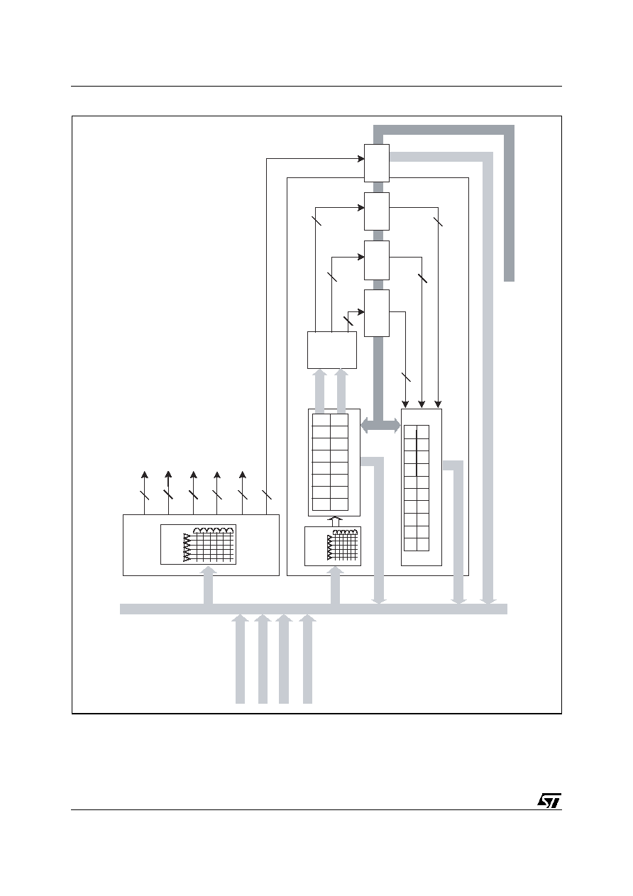
uPSD34xx - PSD MODULE
188/264
Figure 74. DPLD and GPLD
GPLD
20 INPUT MA
CR
OCELLS
PLD INPUT BU
S
PIN FEEDB
A
CK,
POR
TS A,
B,
C
NODE FEEDB
A
C
K
DPLD
Main Flash Memor
y Selects (FSx)
AA
A
A
AA
A
A
BB
B
B
BB
B
B
C
C
C
C
69 INPUTS
OMC
ALLO-
CA
T
O
R
4 or 8
2 or 4
Secondar
y Flash Memor
y Selects (CSBOO
Tx)
1
SRAM Select (RS0)
1
I/O POR
T Select (CSIOP)
2
P
e
r
iper
al I/O Mode Range Selects (PSELx)
1 or 2
Exter
nal De
vice Chip-Selects (ECSx)
8
8
4
8
8
4
AND-OR
ARRA
Y
AND-OR
ARRA
Y
8032 ADDRESS
8032 B
US CONTR
OL
P
A
GE REGISTER
O
THER SIGNALS
16 OUTPUT MA
CR
OCELLS
POR
T A
(80-pin only)
POR
T C
POR
T B
8032 D
A
T
A
B
U
S
PIN FEEDB
A
CK,
POR
T D
POR
T D
8032 D
A
T
A
B
U
S
8 PLD OUT
A
B
A
B
A
B
A
B
A
B
A
B
A
B
A
B
B
C
B
C
B
C
B
C
B
C
B
C
B
C
B
C
8 PLD OUT
69 INPUTS
AI06600A

189/264
uPSD34xx - PSD MODULE
Decode PLD (DPLD). The DPLD (
Figure
75., page 190
) generates the following memory
decode signals:
Eight Main Flash memory sector select signals
(FS0-FS7) with three product terms each
Four Secondary Flash memory sector select
signals (CSBOOT0-CSBOOT3) with three
product terms each
One SRAM select signal (RS0) with two
product terms
One select signal for the base address of 256
PSD Module device control and status
registers (csiop) with one product term
Two external chip-select output signals for
Port D pins, each with one product term (52-
pin devices only have one pin on Port D)
Two chip-select signals (PSEL0, PSEL1) used
to enable the 8032 data bus repeater function
(Peripheral I/O mode) for Port A on 80-pin
devices. Each has one product term.
A product term indicates the logical OR of two or
more inputs. For example, three product terms in
a DPLD output means the final output signal is ca-
pable of representing the logical OR of three differ-
ent input signals, each input signal representing
the logical AND of a combination of the 69 PLD in-
puts.
Using the signal FS0 for example, the user may
create a 3-product term chip select signal that is
logic true when any one of three different address
ranges are true... FS0 = address range 1 OR ad-
dress range 2 OR address range 3.
The phrase "one product term" is a bit misleading,
but commonly used in this context. One product
term is the logical AND of two or more inputs, with
no OR logic involved at all, such as the CSIOP sig-
nal in
Figure 75., page 190
.
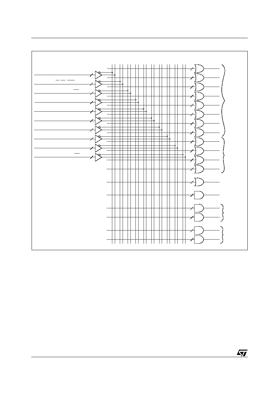
uPSD34xx - PSD MODULE
190/264
Figure 75. DPLD Logic Array
FS0
FS1
FS7
FS6
FS5
FS4
FS3
FS2
MAIN
FLASH
MEMORY
SECTOR
SELECTS
CSBOOT0
CSBOOT3
CSBOOT2
CSBOOT1
SECONDARY
FLASH
MEMORY
SECTOR
SELECTS
RS0
SRAM
SELECT
CSIOP
I/O & CONTROL
REGISTERS
SELECT
ECS0
ECS1
EXTERNAL
CHIP-
SELECTS
(PORT D)
PSEL0
PSEL1
PERIPHERAL
I/O MODE
RANGE
SELECTS
8032 ADDRESS (A0 - A15)
16
4
1
POWER-DOWN INDICATOR (PDN)
1
PIN INPUT PORTS A, B, C (IMCs)
20
PIN INPUT PORT D
2
OMC FEEDBACK (MCELLAB.FB0-7)
8
PAGE REGISTER (PGR0 - PGR7)
8
8
1
OMC FEEDBACK (MCELLBC.FB0-7)
PLD INPUT BUS
3
3
3
3
3
3
3
3
3
3
3
3
2
1
1
1
1
1
NUMBER OF
PRODUCT TERMS
AI06601A
PSM MODULE RESET (RST)
FLASH MEM PROG STATUS (RDYBSY)
8032 CNTL (RD, WR, PSEN, ALE)

191/264
uPSD34xx - PSD MODULE
General PLD (GPLD). The GPLD is used to cre-
ate general system logic.
Figure 74., page 188
shows the architecture of the entire GPLD, and
Figure 76., page 192
shows the relationship be-
tween one OMC, one IMC, and one I/O port pin,
which is representative of pins on Ports A, B, and
C. It is important to understand how these ele-
ments work together. A more detailed description
will follow for the three major blocks (OMC, IMC, I/
O Port) shown in Figure
76
. Figure
76
also shows
which csiop registers to access for various PLD
and I/O functions.
The GPLD contains:
16 Output Macrocells (OMC)
20 Input Macrocells (IMC)
OMC Allocator
Product Term Allocator inside each OMC
AND-OR Array capable of generating up to
137 product terms
Three I/O Ports, A, B, and C
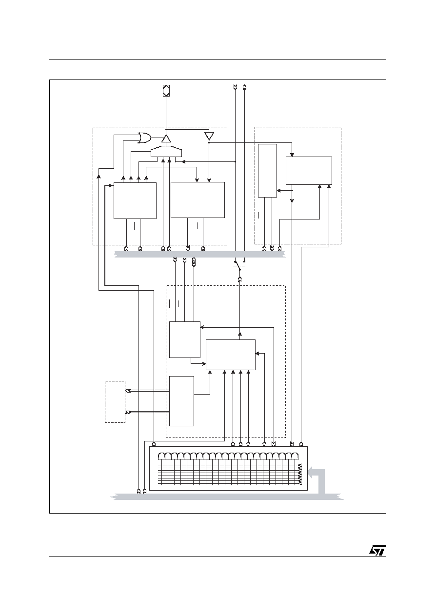
uPSD34xx - PSD MODULE
192/264
Figure 76. GPLD: One OMC, One IMC, and One I/O Port (typical pin, Port A, B, or C)
OUTPUT MA
CR
OCELL (OMC)
INPUT MA
CR
OCELL (IMC)
FLIP-FLOP CLOCK
GLOBAL CLOCK
FLIP-FLOP CLEAR
NODE FEEDBA
CK
NA
TIVE PR
ODUCT
TERMS
PR
ODUCT TERM
ALLOCA
T
O
R
PR
ODUCT
TERMS FR
OM
O
THER OMCs
I/O POR
T
LOGIC
PERIPHERAL I/O MODE BIT
OUTPUT ENABLE
LA
TCHED 8032 ADDR BIT
PSD
MODULE
POR
T PIN
8032 D
A
T
A
BIT
8032 D
A
T
A
BIT
OUTPUT ENABLE
PIN FEEDBA
CK
CLOCK or GA
TE SIGNAL
PLD INPUT BU
S
OMC OUT
ALE
T
O
O
THER
I/O POR
T
LOGIC
OMC
ALLO-
CA
T
O
R
RESET
PSD MODULE RESET
FR
OM
O
THER
MA
CR
OCELL
ALLOCA
T
O
R
GLOBAL CLOCK
AND-OR ARRA
Y
CLOCK or GA
TE
RESET
FLIP-FLOP
AND
O
THER
LOGIC
BORR
O
WED
PR
ODUCT
TERMS
PIN
INPUT
LA
TCH
OR
P
ASS
INPUT
SIGNAL
8032
D
A
T
A
BITS
8032
D
A
T
A
BITS
CSIOP
REGISTERS
(D
A
T
A
OUT
,
DIRECTION
CONTR
OL,
DRIVE)
M
U
X
OMC OUTPUT
FEED
BA
CK
DIRECTION
CONTR
OL
D
A
T
A
OUT
CSIOP
REGISTERS
(D
A
T
A
IN,
D
A
T
A
OUT
,
DIRECTION,
CONTR
OL,
DRIVE,
ENABLE)
CSIOP
REGISTERS
(MCELLAB,
MCELLBC)
READ
OMC
LO
AD
OMC
CSIOP REGISTERS
(IMCA,
IMCB,
IMCC)
READ IMC
FLIP-FLOP PRESET
PIN
INPUT
D
ATA
I
N
69 INPUTS
8032 RD
8032 RD
8032 RD
8032 WR
8032 WR
8032 ADDRESS, D
ATA
, CONTR
OL BU
S
AI06602A
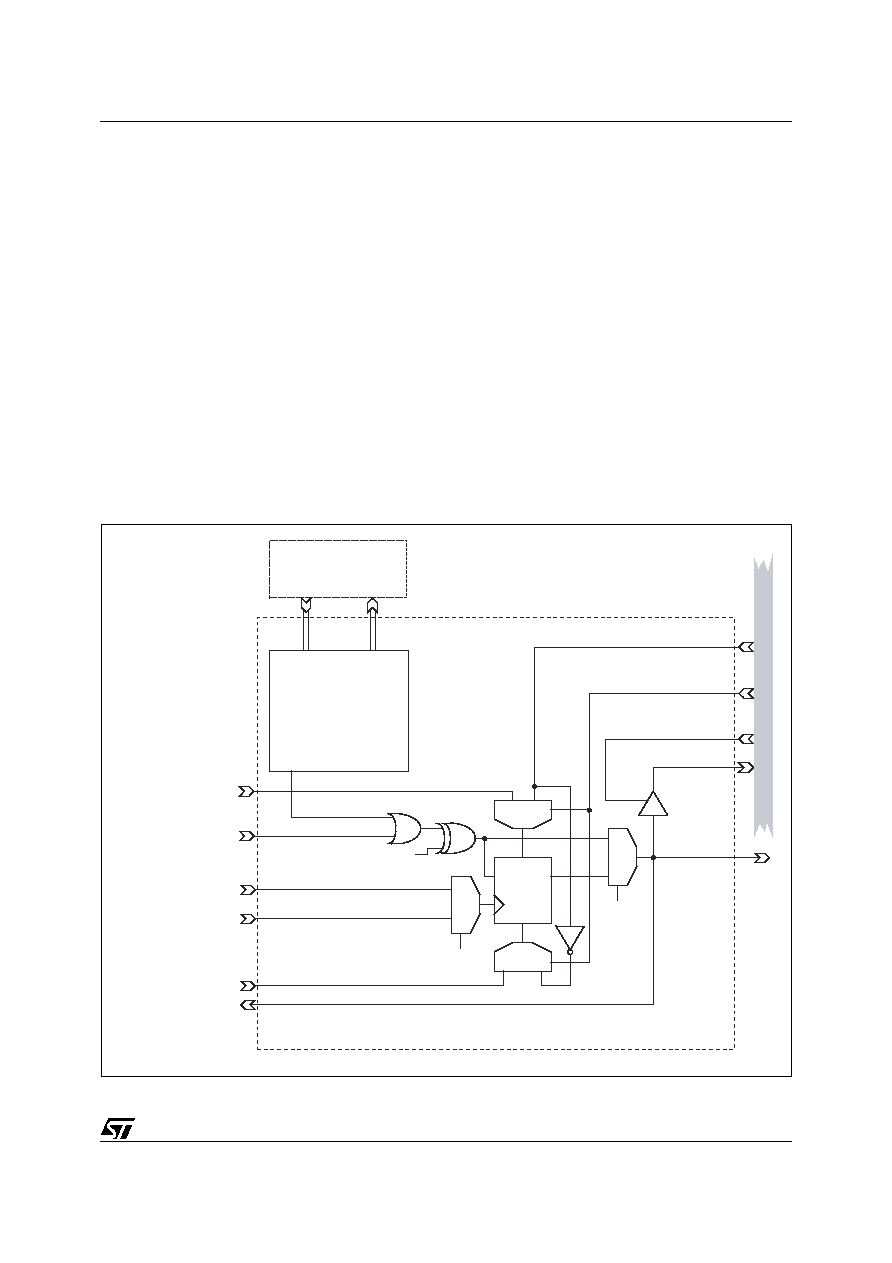
193/264
uPSD34xx - PSD MODULE
Output Macrocell. The GPLD has 16 OMCs. Ar-
chitecture of one individual OMC is shown in Fig-
ure
77
. OMCs can be used for internal node
feedback (buried registers to build shift registers,
etc.), or their outputs may be routed to external
port pins. The user can choose any mixture of
OMCs used for buried functions and OMCs used
to drive port pins.
Referring to Figure
77
, for each OMC there are na-
tive product terms available from the AND-OR Ar-
ray to form logic, and also borrowed product terms
are available (if unused) from other OMCs. The
polarity of the final product term output is con-
trolled by the XOR gate. Each OMC can imple-
ment sequential logic using the flip-flop element,
or combinatorial logic when bypassing the flip-flop
as selected by the output multiplexer. An OMC
output can drive a port pin through the OMC Allo-
cator, it can also drive the 8032 data bus, and also
it can drive a feedback path to the AND-OR Array
inputs, all at the same time.
The flip-flop in each OMC can be synthesized as a
D, T, JK, or SR type in PSDsoft Express. OMC flip-
flops are specified using PSDsoft Express in the
"User Defined Nodes" section of the Design Assis-
tant. Each flip-flop's clock, preset, and clear inputs
may be driven individually from a product term of
the AND-OR Array, defined by equations in PSD-
soft Express for signals *. c, *.pr, and *.re respec-
tively. The preset and clear inputs on the flip-flops
are level activated, active-high logic signals. The
clock inputs on the flip-flops are rising-edge logic
signals.
Optionally, the signal CLKIN (pin PD1) can be
used for a common clock source to all OMC flip-
flops. Each flip-flop is clocked on the rising edge.
A common clock is specified in PSDsoft Express
by assigning the function "Common Clock Input"
for pin PD1 in the Pin Definition section, and then
choosing the signal CLKIN when specifying the
clock input (*.c) for individual flip-flops in the "User
Defined Nodes" section.
Figure 77. Detail of a Single OMC
D
CLR
PRE
Q
MUX
MUX
M
U
X
M
U
X
PSDsoft
PSDsoft
OUTPUT MACROCELL (OMC)
PT PRESET (.PR)
FROM AND-OR ARRAY
BORROWED
PTs
PT CLEAR (.RE)
NODE FEEDBACK (.FB)
POLARITY
SELECT,
PSDsoft
PT ALLOCATOR,
DRAWS FROM LOCAL
AND GLOBAL UNUSED
PRODUCT TERMS.
PSDsoft DICTATES.
LENDED
PTs
DATA BIT FROM 8032
DATA BIT TO 8032
INDICATES MCU WRITE
TO PARTICULAR CSIO
OMC REGISTER
MCU OVERRIDES
PT PRESET AND
CLR DURING
MCU WRITE
MCU READ OF
PARTICULAR CSIOP
OMC REGISTER
OMC
OUTPUT
FROM AND-OR ARRAY
TO PLD INPUT BUS
FROM AND-OR ARRAY
NATIVE PTs
ALLOCATED PTs
PT CLOCK (.C)
FROM AND-OR ARRAY
GLOBAL CLOCK (CLKIN)
FROM PLD INPUT BUS
8032 ADDRESS,
D
A
T
A
,
CONTR
OL B
U
S
OMC
ALLO-
CATOR
O
U
T
PRODUCT TERMS
FROM OTHER
OMCs
AI06617A

uPSD34xx - PSD MODULE
194/264
OMC Allocator. Outputs of the 16 OMCs can be
routed to a combination of pins on Port A (80-pin
devices only), Port B, or Port C as shown in Figure
78
. OMCs are routed to port pins automatically af-
ter specifying pin numbers in PSDsoft Express.
Routing can occur on a bit-by-bit basis, spitting
OMC assignment between the ports. However,
one OMC can be routed to one only port pin, not
both ports.
Product Term Allocator. Each OMC has a Prod-
uct Term Allocator as shown in
Figure
77., page 193
. PSDsoft Express uses PT Alloca-
tors to give and take product terms to and from
other OMCs to fit a logic design into the available
silicon resources. This happens automatically in
PSDsoft Express, but understanding how PT allo-
cation works will help if the logic design does not
"fit", in which case the user may try selecting a dif-
ferent pin or different OMC for the logic where
more product terms may be available. The follow-
ing list summarizes how product terms are allocat-
ed to each OMC, as shown in
Table
112., page 195
.
≠
MCELLAB0-MCELLAB7 each have three
native product terms and may borrow up to six
more
≠
MCELLBC0-MCELLBC3 each have four
native product terms and may borrow up to
five more
≠
MCELLBC4-MCELLBC7 each have four
native product terms and may borrow up to six
more.
Native product terms come from the AND-OR Ar-
ray. Each OMC may borrow product terms only
from certain other OMCs, if they are not in use.
Product term allocation does not add any propaga-
tion delay to the logic. The fitter report generated
by PSDsoft Express will show any PT allocation
that has occurred.
If an equation requires more product terms than
are available to it through PT allocation, then "ex-
ternal" product terms are required, which con-
sumes other OMCs. This is called product term
expansion and also happens automatically in PS-
Dsoft Express as needed. PT expansion causes
additional propagation delay because an addition-
al OMC is consumed by the expansion process
and its output is rerouted (or fed back) into the
AND-OR array. The user can examine the fitter re-
port generated by PSDsoft Express to see result-
ing PT allocation and PT expansion (expansion
will have signal names, such as `*.fb_0' or `*.fb_1').
PSDsoft Express will always try to fit the logic de-
sign first by using PT allocation, and if that is not
sufficient then PSDsoft Express will use PT expan-
sion.
Product term expansion may occur in the DPLD
for complex chip select equations for Flash mem-
ory sectors and for SRAM, but this is a rare oc-
curence. If PSDsoft Express does use PT
expansion in the DPLD, it results in an approxi-
mate 15ns additional propagation delay for that
chip select signal, which gives 15ns less time for
the memory to respond. Be aware of this and con-
sider adding a wait state to the 8032 bus access
(using the SFR named, BUSCON), or lower the
8032 clock frequency to avoid problems with
memory access time.
Figure 78. OMC Allocator
PORT C PINS
PORT B PINS
PORT A PINS
(80-pin pkg only)
OMC Bank BC (MCELLBC0-7)
OMC Bank AB (MCELLAB0-7)
0
1
2
3
4
5
6
7
0
1
2
3
4
5
6
7
2
3
4
7
4
5
6
7
3 2 1 0
4
5
6
7
3 2 1 0
*
*
*
*
* = Used for JTAG,
Pin Not Available
to GPLD
AI09177

195/264
uPSD34xx - PSD MODULE
Table 112. OMC Port and Data Bit Assignments
Note: 1. MCELLAB0-MCELLAB7 can be output to Port A pins only on 80-pin devices. Port A is not available on 52-pin devices
2. Port pins PC0, PC1, PC5, and PC6 are dedicated JTAG pins and are not available as outputs for MCELLBC 0, 1, 5, or 6
OMC
Port
Assignment
(1,2)
Native Product Terms
from AND-OR Array
Maximum Borrowed
Product Terms
Data Bit on 8032 Data
Bus for Loading or
Reading OMC
MCELLAB0
Port A0 or B0
3
6
D0
MCELLAB1
Port A1 or B1
3
6
D1
MCELLAB2
Port A2 or B2
3
6
D2
MCELLAB3
Port A3 or B3
3
6
D3
MCELLAB4
Port A4 or B4
3
6
D4
MCELLAB5
Port A5 or B5
3
6
D5
MCELLAB6
Port A6 or B6
3
6
D6
MCELLAB7
Port A7 or B7
3
6
D7
MCELLBC0
Port B0
4
5
D0
MCELLBC1
Port B1
4
5
D1
MCELLBC2
Port B or C2
4
5
D2
MCELLBC3
Port B3 or C3
4
5
D3
MCELLBC4
Port B4 or C4
4
6
D4
MCELLBC5
Port B5
4
6
D5
MCELLBC6
Port B6
4
6
D6
MCELLBC7
Port B7 orC7
4
6
D7
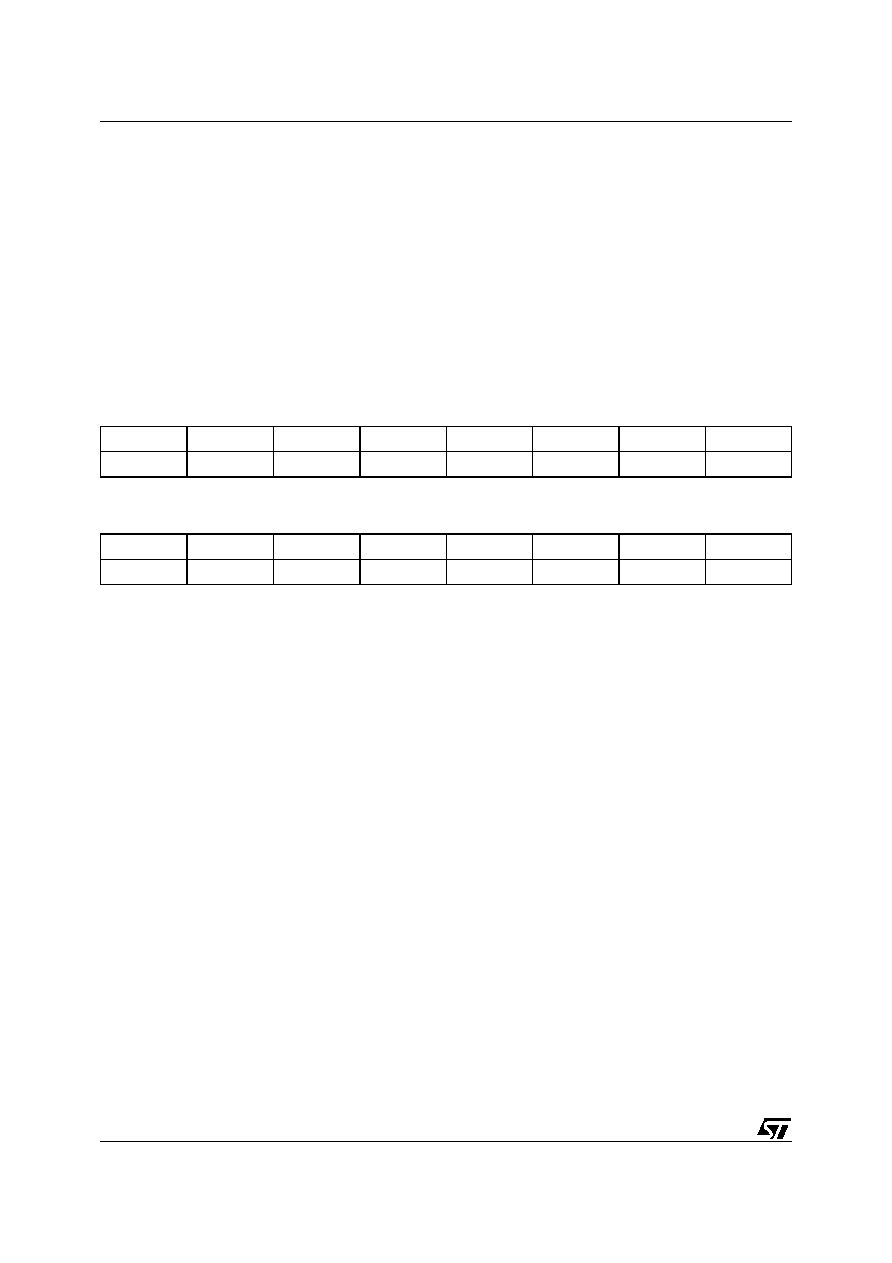
uPSD34xx - PSD MODULE
196/264
Loading and Reading OMCs. Each of the two
OMC groups (eight OMCs each) occupies a byte
in csiop space, named MCELLAB and MCELLBC
(see Table
113
and Table
114
). When the 8032
writes or reads these two OMC registers in csiop it
is accessing each of the OMCs through its 8-bit
data bus, with the bit assignment shown in
Table
112., page 195
. Sometimes it is important to know
the bit assignment when the user builds GPLD log-
ic that is accessed by the 8032. For example, the
user may create a 4-bit counter that must be load-
ed and read by the 8032, so the user must know
which nibble in the corresponding csiop OMC reg-
ister the firmware must access. The fitter report
generated by PSDsoft Express will indicate how it
assigned the OMCs and data bus bits to the logic.
The user can optionally force PSDsoft Express to
assign logic to specific OMCs and data bus bits if
desired by using the `PROPERTY' statement in
PSDsoft Express. Please see the PSDsoft Ex-
press User's Manual for more information on OMC
assignments.
Loading the OMC flip-flops with data from the
8032 takes priority over the PLD logic functions.
As such, the preset, clear, and clock inputs to the
flip-flop can be asynchronously overridden when
the 8032 writes to the csiop registers to load the in-
dividual OMCs.
Table 113. Output Macrocell MCELLAB (address = csiop + offset 20h)
Note: All bits clear to logic '0' at power-on reset, but do not clear after warm reset conditions (non-power-on reset)
Table 114. Output Macrocell MCELLBC (address = csiop + offset 21h)
Note: All bits clear to logic '0' at power-on reset, but do not clear after warm reset conditions (non-power-on reset)
Bit 7
Bit 6
Bit 5
Bit 4
Bit 3
Bit 2
Bit 1
Bit 0
MCELLAB7
MCELLAB6
MCELLAB5
MCELLAB4
MCELLAB3
MCELLAB2
MCELLAB1
MCELLAB0
Bit 7
Bit 6
Bit 5
Bit 4
Bit 3
Bit 2
Bit 1
Bit 0
MCELLBC7
MCELLBC6
MCELLBC5
MCELLBC4
MCELLBC3
MCELLBC2
MCELLBC1
MCELLBC0
197/264
uPSD34xx - PSD MODULE
OMC Mask Registers. There is one OMC Mask
Register for each of the two groups of eight OMCs
shown in Table
115
and Table
116
. The OMC
mask registers are used to block loading of data to
individual OMCs. The default value for the mask
registers is 00h, which allows loading of all OMCs.
When a given bit in a mask register is set to a '1,'
the 8032 is blocked from writing to the associated
OMC flip-flop. For example, suppose that only four
of eight OMCs (MCELLAB0-3) are being used for
a state machine. The user may not want the 8032
to write to all the OMCs in MCELLAB because it
would overwrite the state machine registers.
Therefore, the user would want to load the mask
register for MCELLAB with the value 0Fh before
writing OMCs.
Table 115. Output Macrocell MCELLAB Mask Register (address = csiop + offset 22h)
Note: 1. Default is 00h after any reset condition
2. 1 = block writing to individual macrocell, 0 = allow writing to individual macrocell
Table 116. Output Macrocell MCELLBC Mask Register (address = csiop + offset 23h)
Note: 1. Default is 00h after any reset condition
2. 1 = block writing to individual macrocell, 0 = allow writing to individual macrocell
Input Macrocells. The GPLD has 20 IMCs, one
for each pin on Port A (80-pin device only), one for
each pin on Port B, and for the four pins on Port C
that are not JTAG pins. The architecture of one in-
dividual IMC is shown in
Figure 79., page 198
.
IMCs are individually configurable, and they can
strobe a signal coming in from a port pin as a latch
(gated), or as a register (clocked), or the IMC can
pass the signal without strobing, all prior to driving
the signal onto the PLD input bus. Strobing is use-
ful for sampling and debouncing inputs (keypad in-
puts, etc.) before entering the PLD AND-OR
arrays. The outputs of IMCs can be read by the
8032 asynchronously when the 8032 reads the
csiop registers shown in Table
117
, Table
118
,
and
Table 119., page 198
. It is possible to read a
PSD Module port pin using one of two different
methods, one method is by reading IMCs as de-
scribed here, the other method is using MCU I/O
mode described in a later section.
The optional IMC clocking or gating signal used to
strobe pin inputs is driven by a product term from
the AND-OR array. There is one clocking or gating
product term available for each group of four
IMCs. Port inputs 0-3 are controlled by one prod-
uct term and 4-7 by another. To specify in PSDsoft
Express the method in which a signal will be
strobed as it enters an IMC for a given input pin on
Port A, B, or C, just specify "PT Clocked Register"
to use a rising edge to clock the incoming signal,
or specify "PT Clock Latch" to use an active high
gate signal to latch the incoming signal. Then de-
fine an equation for the IMC clock (.ld) or the IMC
gate (.le) signal in the "I/O Equations" section.
If the user would like to latch an incoming signal
using the gate signal ALE from the 8032, then in
PSDsoft Express, for a given input pin on Port A,
B, or C, specify "Latched Address" as the pin func-
tion.
If it is desired to pass an incoming signal through
an IMC directly to the AND-OR array inputs with-
out clocking or gating (this is most common), in
PSDsoft Express simply specify "Logic or Ad-
dress" for the input pin function on Port A, B, or C.
Bit 7
Bit 6
Bit 5
Bit 4
Bit 3
Bit 2
Bit 1
Bit 0
Mask
MCELLAB7
Mask
MCELLAB6
Mask
MCELLAB5
Mask
MCELLAB4
Mask
MCELLAB3
Mask
MCELLAB2
Mask
MCELLAB1
Mask
MCELLAB0
Bit 7
Bit 6
Bit 5
Bit 4
Bit 3
Bit 2
Bit 1
Bit 0
Mask
MCELLBC7
Mask
MCELLBC6
Mask
MCELLBC5
Mask
MCELLBC4
Mask
MCELLBC3
Mask
MCELLBC2
Mask
MCELLBC1
Mask
MCELLBC0
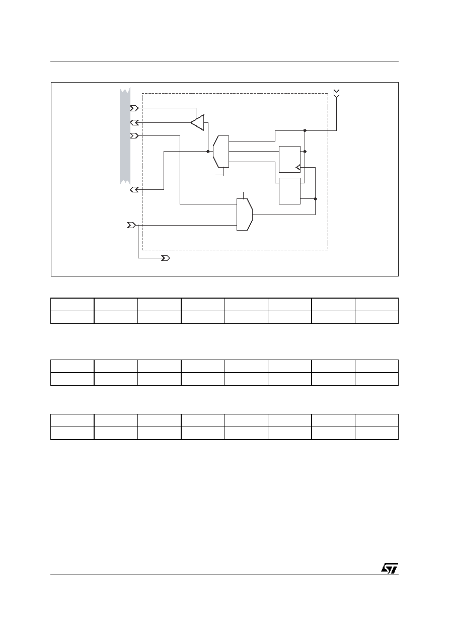
uPSD34xx - PSD MODULE
198/264
Figure 79. Detail of a Single IMC
Table 117. Input Macrocell Port A
(1)
(address = csiop + offset 0Ah)
Note: 1. Port A not available on 52-pin uPSD34xx devices
2. 1 = current state of IMC is logic '1,' 0 = current state is logic '0'
Table 118. Input Macrocell Port B (address = csiop + offset 0Bh)
Note: 1 = current state of IMC is logic '1,' 0 = current state is logic '0'
Table 119. Input Macrocell Port C (address = csiop + offset 18h)
Note: 1. X = Not guaranteed value, can be read either '1' or '0.' These are JTAG pins.
2. 1 = current state of IMC is logic '1,' 0 = current state is logic '0'
Bit 7
Bit 6
Bit 5
Bit 4
Bit 3
Bit 2
Bit 1
Bit 0
IMC PA7
IMC PA6
IMC PA5
IMC PA4
IMC PA3
IMC PA2
IMC PA1
IMC PA0
Bit 7
Bit 6
Bit 5
Bit 4
Bit 3
Bit 2
Bit 1
Bit 0
IMC PB7
IMC PB6
IMC PB5
IMC PB4
IMC PB3
IMC PB2
IMC PB1
IMC PB0
Bit 7
Bit 6
Bit 5
Bit 4
Bit 3
Bit 2
Bit 1
Bit 0
IMC PC7
X
X
IMC PC4
IMC PC3
IMC PC2
X
X
INPUT MACROCELL (IMC)
D
Q
G
D
Q
M
U
X
M
U
X
PSDsoft
8032 DATA BIT
8032 READ OF PARTICULAR CSIOP IMC REGISTER
PT CLOCK OR GATE (.LD OR .LE)
PIN INPUT
LATCHED INPUT
GATED INPUT
(.LD)
(.LE)
ALE
PSDsoft
ALE
8032 ADDR,
D
A
T
A
,
CNTL B
U
S
FROM I/O PORT
LOGIC
INPUT SIGNAL
FROM PIN ON
PORT A, B, or C
FROM AND-OR ARRAY
TO PLD INPUT BUS
THIS SIGAL IS GANGED TO 3 OTHER
IMCs, GROUPING IMC 0 - 3 or IMC 4 - 7.
AI06603A

199/264
uPSD34xx - PSD MODULE
I/O Ports. There are four programmable I/O ports
on the PSD Module: Port A (80-pin device only),
Port B, Port C, and Port D. Ports A and B are eight
bits each, Port C is four bits, and Port D is two bits
for 80-pin devices or 1-bit for 52-pin devices. Each
port pin is individually configurable, thus allowing
multiple functions per port. The ports are config-
ured using PSDsoft Express then programming
with JTAG, and also by the 8032 writing to csiop
registers at run-time.
Topics discussed in this section are:
General Port architecture
Port Operating Modes
Individual Port Structure
General Port Architecture. The general archi-
tecture for a single I/O Port pin is shown in
Figure
80., page 200
. Port structures for Ports A, B, C,
and D differ slightly and are shown in
Figure
85., page 212
though
Figure 88., page 217
.
Figure 80., page 200
shows four csiop registers
whose outputs are determined by the value that
the 8032 writes to csiop Direction, Drive, Control,
and Data Out. The I/O Port logic contains an out-
put mux whose mux select signal is determined by
PSDsoft Express and the csiop Control register
bits at run-time. Inputs to this output mux include
the following:
1.
Data from the csiop Data Out register for MCU
I/O output mode (All ports)
2.
Latched de-multiplexed 8032 Address for
Address Output mode (Ports A and B only)
3.
Peripheral I/O mode data bit (Port A only)
4.
GPLD OMC output (Ports A, B, and C).
The Port Data Buffer (PDB) provides feedback to
the 8032 and allows only one source at a time to
be read when the 8032 reads various csiop regis-
ters. There is one PDB for each port pin enabling
the 8032 to read the following on a pin-by-pin ba-
sis:
1.
MCU I/O signal direction setting (csiop
Direction reg)
2.
Pin drive type setting (csiop Drive Select reg)
3.
Latched Addr Out mode setting (csiop Control
reg)
4.
MCU I/O pin output setting (csiop Data Out
reg)
5.
Output Enable of pin driver (csiop Enable Out
reg)
6.
MCU I/O pin input (csiop Data In reg)
A port pin's output enable signal is controlled by a
two input OR gate whose inputs come from: a
product term of the AND-OR array; the output of
the csiop Direction Register. If an output enable
from the AND-OR Array is not defined, and the
port pin is not defined as an OMC output, and if
Peripheral I/O mode is not used, then the csiop Di-
rection Register has sole control of the OE signal.
As shown in
Figure 80., page 200
, a physical port
pin is connected to the I/O Port logic and is also
separately routed to an IMC, allowing the 8032 to
read a port pin by two different methods (MCU I/O
input mode or read the IMC).
Port Operating Modes. I/O Port logic has sever-
al modes of operation.
Table 115., page 197
sum-
marizes which modes are available on each port.
Each of the port operating modes are described in
following sections. Some operating modes can be
defined using PSDsoft Express, and some by the
8032 writing to the csiop registers at run-time, and
some require both. For example, PLD I/O, Latched
Address Out, and Peripheral I/O modes must be
defined in PSDsoft Express and programmed into
the device using JTAG, but an additional step
must happen at run-time to activate Latched Ad-
dress Out mode and Peripheral I/O mode, but not
needed for PLD I/O. In another example, MCU I/O
mode is controlled completely by the 8032 at run-
time and only a simple pin name declaration is
needed in PSDsoft Express for documentation.
Table 116., page 197
summarizes what actions
are needed in PSDsoft Express and what actions
are required by the 8032 at run-time to achieve the
various port functions.

uPSD34xx - PSD MODULE
200/264
Figure 80. Detail of a Single I/O Port (typical of Ports A, B, C)
I/O PORT
LOGIC
O
U
T
P
U
T
M
U
X
P
D
B
M
U
X
DIRECTION
DRIVE SELECT
CONTROL
DATA OUT (MCUI/O)
ENABLE OUT
DATA IN (MCUI/O)
D BIT, PERIPH I/O MODE, Port A
PT OUTPUT ENABLE (.OE)
LATCHED ADDR BIT, PORT A or B
OE
MUX
8032
DATA
BIT
OUTPUT
DRIVER
TYPICAL
PIN
PORT A, B, C
PSD MODULE RESET
ONE of 6
CSIOP
REGISTERS
OUTPUT
SELECT
PERIPHERAL I/O
MODE SETS
DIRECTION
(PORT A ONLY)
8032 ADDRESS,
D
A
T
A
,
CONTR
OL B
U
S
1
2
3
4
1
2
3
4
5
6
FROM OMC OUTPUT
TO IMC
FROM PLD INPUT BUS
FROM AND-OR ARRAY
FROM OMC
ALLOCATOR
D
CLR
DIRECTION
DRIVE
CONTROL
(MCUI/O)
DATA OUT
RESET
PSDsoft
PSELx
PERIPH I/O
DATA BIT
CSIOP
REGIS-
TERS
Q
Q
Q
Q
DRIVE TYPE
8032
DATA
BITS
INPUT
BUFFER
OUTPUT ENABLE
WR
RD PIO EN
8032
WR
8032 RD
AI07873A

201/264
uPSD34xx - PSD MODULE
Table 120. Port Operating Modes
Note: 1. MCELLBC outputs available only on pins PC2, PC3, PC4, and PC7.
2. JTAG pins (PC0/TMS, PC1/TCK, PC5/TDI, PC6/TDO) are dedicated to JTAG pin functions (cannot be used for general I/O).
Port Operating Mode
Port A (80-pin only)
Port B
Port C
Port D
Find it
MCU I/O
Yes
Yes
Yes
Yes
MCU I/O
Mode., p
age 203
PLD I/O
OMC MCELLAB Outputs
OMC MCELLBC Outputs
External Chip-Select Outputs
PLD Inputs
Yes
No
No
Yes
Yes
Yes
No
Yes
No
Yes
(1)
No
Yes
No
No
Yes
Yes
PLD I/O
Mode., p
age 205
Latched Address Output
Yes
Yes
No
No
Latched
Address
Output
Mode, pa
ge 208
Peripheral I/O Mode
Yes
No
No
No
Peripher
al I/O
Mode, pa
ge 209
JTAG ISP
No
No
Yes
(2)
No
JTAG
ISP
Mode., p
age 210

uPSD34xx - PSD MODULE
202/264
Table 121. Port Configuration Setting Requirements
Port
Operating
Mode
Required Action in
PSDsoft Express to
Configure each Pin
Value that 8032
writes to csiop
Control Register at
run-time
Value that 8032
writes to csiop
Direction Register
at run-time
Value that 8032
writes to Bit 7
(PIO_EN) of csiop VM
Register at run-time
MCU I/O
Choose the MCU I/O
function and declare the
pin name
Logic '0' (default)
Logic 1 = Out of
uPSD
Logic 0 = Into uPSD
N/A
PLD I/O
Choose the PLD function
type, declare pin name,
and specify logic
equation(s)
N/A
Direction register
has no effect on a
pin if pin is driven
from OMC output
N/A
Latched Address
Output
Choose Latched Address
Out function, declare pin
name
Logic '1'
Logic '1' Only
N/A
Peripheral I/O
Choose Peripheral I/O
mode function and
specify address range in
DPLD for PSELx
N/A
N/A
PIO_EN Bit = Logic 1
(default is '0')
4-PIN JTAG ISP
No action required in
PSDsoft to get 4-pin
JTAG. By default TDO,
TDI, TCK, TMS are
dedicated JTAG
functions.
N/A
N/A
N/A
6-PIN JTAG ISP
(faster
programming)
Choose JTAG TSTAT
function for pin PC3 and
JTAG TERR function for
pin PC4.
N/A
N/A
N/A
203/264
uPSD34xx - PSD MODULE
MCU I/O Mode. In MCU I/O mode, the 8032 on
the MCU Module expands its own I/O by using the
I/O Ports on the PSD Module. The 8032 can read
PSD Module I/O pins, set the direction of the I/O
pins, and change the output state of I/O pins by ac-
cessing the Data In, Direction, and Data Out csiop
registers respectively at run-time.
To implement MCU I/O mode, each desired pin is
specified in PSDsoft Express as MCU I/O function
and given a pin name. Then 8032 firmware is writ-
ten to set the Direction bit for each corresponding
pin during initialization routines (0 = In, 1 = Out of
the chip), then the 8032 firmware simply reads the
corresponding Data In register to determine the
state of an I/O pin, or writes to a Data Out register
to set the state of a pin. The Direction of each pin
may be changed dynamically by the 8032 if de-
sired. A mixture of input and output pins within a
single port is allowed.
Figure 80., page 200
shows
the Data In, Data Out, and Direction signal paths.
The Data In registers are defined in Table
122
to
Table
125
. The Data Out registers are defined in
Table
126
to
Table 129., page 204
. The Direction
registers are defined in Table
130
to
Table
133., page 204
.
Table 122. MCU I/O Mode Port A Data In Register
(1)
(address = csiop + offset 00h)
Note: 1. Port A not available on 52-pin uPSD34xx devices
2. For each bit, 1 = current state of input pin is logic '1,' 0 = current state is logic '0'
Table 123. MCU I/O Mode Port B Data In Register (address = csiop + offset 01h)
Note: For each bit, 1 = current state of input pin is logic '1,' 0 = current state is logic '0'
Table 124. MCU I/O Mode Port C Data In Register (address = csiop + offset 10h)
Note: 1. X = Not guaranteed value, can be read either '1' or '0.'
2. For each bit, 1 = current state of input pin is logic '1,' 0 = current state is logic '0'
Table 125. MCU I/O Mode Port D Data In Register (address = csiop + offset 11h)
Note: 1. X = Not guaranteed value, can be read either '1' or '0.'
2. For each bit, 1 = current state of input pin is logic '1,' 0 = current state is logic '0'
3. Not available on 52-pin uPSD34xx devices
Table 126. MCU I/O Mode Port A Data Out Register
(1)
(address = csiop + offset 04h)
Note: 1. Port A not available on 52-pin uPSD34xx devices
2. For each bit, 1 = drive port pin to logic '1,' 0 = drive port pin to logic '0'
3. Default state of register is 00h after reset or power-up
Table 127. MCU I/O Mode Port B Data Out Register (address = csiop + offset 05h)
Note: 1. For each bit, 1 = drive port pin to logic '1,' 0 = drive port pin to logic '0'
2. Default state of register is 00h after reset or power-up
Bit 7
Bit 6
Bit 5
Bit 4
Bit 3
Bit 2
Bit 1
Bit 0
PA7
PA6
PA5
PA4
PA3
PA2
PA1
PA0
Bit 7
Bit 6
Bit 5
Bit 4
Bit 3
Bit 2
Bit 1
Bit 0
PB7
PB6
PB5
PB4
PB3
PB2
PB1
PB0
Bit 7
Bit 6
Bit 5
Bit 4
Bit 3
Bit 2
Bit 1
Bit 0
PC7
X
X
PC4
PC3
PC2
X
X
Bit 7
Bit 6
Bit 5
Bit 4
Bit 3
Bit 2
Bit 1
Bit 0
X
X
X
X
X
PD2
(3)
PD1
X
Bit 7
Bit 6
Bit 5
Bit 4
Bit 3
Bit 2
Bit 1
Bit 0
PA7
PA6
PA5
PA4
PA3
PA2
PA1
PA0
Bit 7
Bit 6
Bit 5
Bit 4
Bit 3
Bit 2
Bit 1
Bit 0
PB7
PB6
PB5
PB4
PB3
PB2
PB1
PB0
uPSD34xx - PSD MODULE
204/264
Table 128. MCU I/O Mode Port C Data Out Register (address = csiop + offset 12h)
Note: 1. For each bit, 1 = drive port pin to logic '1,' 0 = drive port pin to logic '0'
2. Default state of register is 00h after reset or power-up
Table 129. MCU I/O Mode Port D Data Out Register (address = csiop + offset 13h)
Note: 1. For each bit, 1 = drive port pin to logic '1,' 0 = drive port pin to logic '0'
2. Default state for register is 00h after reset or power-up
3. Not available on 52-pin uPSD34xx devices
Table 130. MCU I/O Mode Port A Direction Register
(1)
(address = csiop + offset 06h)
Note: 1. Port A not available on 52-pin uPSD34xx devices
2. For each bit, 1 = out from uPSD34xx port pin1, 0 = in to PSD34xx port pin
3. Default state for register is 00h after reset or power-up
Table 131. MCU I/O Mode Port B Direction In Register (address = csiop + offset 07h)
Note: 1. For each bit, 1 = out from uPSD34xx port pin1, 0 = in to PSD34xx port pin
2. Default state for register is 00h after reset or power-up
Table 132. MCU I/O Mode Port C Direction Register (address = csiop + offset 14h)
Note: 1. For each bit, 1 = out from uPSD34xx port pin1, 0 = in to PSD34xx port pin
2. Default state for register is 00h after reset or power-up
Table 133. MCU I/O Mode Port D Direction Register (address = csiop + offset 15h)
Note: 1. For each bit, 1 = out from uPSD34xx port pin1, 0 = in to PSD34xx port pin
2. Default state for register is 00h after reset or power-up
3. Not available on 52-pin uPSD34xx devices
Bit 7
Bit 6
Bit 5
Bit 4
Bit 3
Bit 2
Bit 1
Bit 0
PC7
N/A
N/A
PC4
PC3
PC2
N/A
N/A
Bit 7
Bit 6
Bit 5
Bit 4
Bit 3
Bit 2
Bit 1
Bit 0
N/A
N/A
N/A
N/A
N/A
PD2
(3)
PD1
N/A
Bit 7
Bit 6
Bit 5
Bit 4
Bit 3
Bit 2
Bit 1
Bit 0
PA7
PA6
PA5
PA4
PA3
PA2
PA1
PA0
Bit 7
Bit 6
Bit 5
Bit 4
Bit 3
Bit 2
Bit 1
Bit 0
PB7
PB6
PB5
PB4
PB3
PB2
PB1
PB0
Bit 7
Bit 6
Bit 5
Bit 4
Bit 3
Bit 2
Bit 1
Bit 0
PC7
N/A
N/A
PC4
PC3
PC2
N/A
N/A
Bit 7
Bit 6
Bit 5
Bit 4
Bit 3
Bit 2
Bit 1
Bit 0
N/A
N/A
N/A
N/A
N/A
PD2
(3)
PD1
N/A
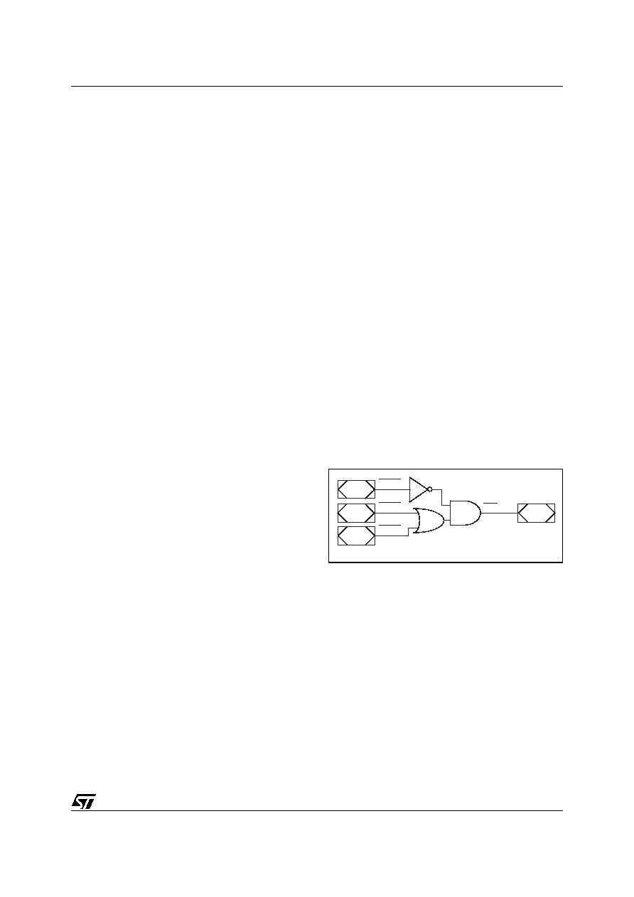
205/264
uPSD34xx - PSD MODULE
PLD I/O Mode. Pins on Ports A, B, C, and D can
serve as inputs to either the DPLD or the GPLD.
Inputs to these PLDs from Ports A, B, and C are
routed through IMCs before reaching the PLD in-
put bus. Inputs to the PLDs from Port D do not
pass through IMCs, but route directly to the PLD
input bus.
Pins on Ports A, B, and C can serve as outputs
from GPLD OMCs, and Port D pins can be outputs
from the DPLD (external chip-selects) which do
not consume OMCs.
Whenever a pin is specified to be a PLD output, it
cannot be used for MCU I/O mode, or other pin
modes. If a pin is specified to be a PLD input, it is
still possible to read the pin using MCU I/O input
mode with the csiop register Data In. Also, the
csiop Direction register can still affect a pin which
is used for a PLD input. The csiop Data Out regis-
ter has no effect on a PLD output pin.
Each pin on Ports A, B, C, and D have a tri-state
buffer at the final output stage. The Output Enable
signal for this buffer is driven by the logical OR of
two signals. One signal is an Output Enable signal
generated by the AND-OR array (from an .oe
equation specified in PSDsoft), and the other sig-
nal is the output of the csiop Direction register.
This logic is shown in
Figure 80., page 200
. At
power-on, all port pins default to high-impedance
input (Direction registers default to 00h). However,
if an equation is written for the Output Enable that
is active at power-on, then the pin will behave as
an output.
PLD I/O equations are specified in PSDsoft Ex-
press and programmed into the uPSD using
JTAG. Figure
81
shows a very simple combinato-
rial logic example which is implemented on pins of
Port B.
To give a general idea of how PLD logic is imple-
mented using PSDsoft Express,
Figure
82., page 206
illustrates the pin declaration win-
dow of PSDsoft Express, showing the PLD output
at pin PB0 declared as "Combinatorial" in the "PLD
Output" section, and a signal name, "pld_out", is
specified. The other three signals on pins PB1,
PB2, and PB3 would be declared as "Logic or Ad-
dress" in the "PLD Input" section, and given signal
names.
In the "Design Assistant" window of PSDsoft Ex-
press shown in
Figure 83., page 207
, the user
simply enters the logic equation for the signal
"pld_out" as shown. The user can either type in the
logic statements or enter them using a point-and-
click method, selecting various signal names and
logic operators available in the window.
After PSDsoft Express has accepted and realized
the logic from the equations, it synthesizes the log-
ic statement:
pld_out = ( pld_in_1 # pld_in_2 ) & !pld_in_3;
to be programmed into the GPLD. See the PSD-
soft User's Manual for all the steps.
Note: If a particular OMC output is specified as an
internal node and not specified as a port pin output
in PSDsoft Express, then the port pin that is asso-
ciated with that OMC can be used for other I/O
functions.
Figure 81. Simple PLD Logic Example
PLDIN 1
PLDIN 2
PLDIN 3
PLD OUT
PB0
PB3
PB2
PB1
AI09178
uPSD34xx - PSD MODULE
206/264
Figure 82. Pin Declarations in PSDsoft Express for Simple PLD Example

207/264
uPSD34xx - PSD MODULE
Figure 83. Using the Design Assistant in PSDsoft Express for Simple PLD Example
uPSD34xx - PSD MODULE
208/264
Latched Address Output Mode. In the MCU
Module, the data bus Bits D0-D15 are multiplexed
with the address Bits A0-A15, and the ALE signal
is used to separate them with respect to time.
Sometimes it is necessary to send de-multiplexed
address signals to external peripherals or memory
devices. Latched Address Output mode will drive
individual demuxed address signals on pins of
Ports A or B. Port pins can be designated for this
function on a pin-by-pin basis, meaning that an en-
tire port will not be sacrificed if only a few address
signals are needed.
To activate this mode, the desired pins on Port A
or Port B are designated as "Latched Address Out"
in PSDsoft. Then in the 8032 initialization firm-
ware, a logic '1' is written to the csiop Control reg-
ister for Port A or Port B in each bit position that
corresponds to the pin of the port driving an ad-
dress signal. Table
134
and Table
135
define the
csiop Control register locations and bit assign-
ments.
The latched low address byte A4-A7 is available
on both Port A and Port B. The high address byte
A8-A15 is available on Port B only. Selection of
high or low address byte is specified in PSDsoft
Express.
Table 134. Latched Address Output, Port A Control Register
(1)
(address = csiop + offset 02h)
Note: 1. Port A not available on 52-pin uPSD34xx devices
2. For each bit, 1 = drive demuxed 8032 address signal on pin, 0 = pin is default mode, MCU I/O
3. Default state for register is 00h after reset or power-up
Table 135. Latched Address Output, Port B Control Register (address = csiop + offset 03h)
Note: 1. For each bit, 1 = drive demuxed 8032 address signal on pin, 0 = pin is default mode, MCU I/O
2. Default state for register is 00h after reset or power-up
Bit 7
Bit 6
Bit 5
Bit 4
Bit 3
Bit 2
Bit 1
Bit 0
PA7
(addr A7)
PA6
(addr A6)
PA5
(addr A5)
PA4
(addr A4)
PA3
(addr A3)
PA2
(Addr A2)
PA1
(addr A1)
PA0
(addr A0)
Bit 7
Bit 6
Bit 5
Bit 4
Bit 3
Bit 2
Bit 1
Bit 0
PB7
(addr A7 or
A15)
PB6
(addr A6 or
A14)
PB5
(addr A5 or
A13)
PB4
(addr A4 or
A12)
PB3
(addr A3 or
A11)
PB2
(Addr A2 or
A10)
PB1
(addr A1 or
A9)
PB0
(addr A0 or
A8)

209/264
uPSD34xx - PSD MODULE
Peripheral I/O Mode. This mode will provide a
data bus repeater function for the 8032 to interface
with external parallel peripherals. The mode is
only available on Port A (80-pin devices only) and
the data bus signals, D0 - D7, are de-multiplexed
(no address A0-A7). When active, this mode be-
haves like a bidirectional buffer, with the direction
automatically controlled by the 8032 RD and WR
signals for a specified address range. The DPLD
signals PSEL0 and PSEL1 determine this address
range.
Figure 80., page 200
shows the action of
Peripheral I/O mode on the Output Enable logic of
the tri-state output driver for a single port pin.
Fig-
ure 84., page 209
illustrates data repeater the op-
eration. To activate this mode, choose the pin
function "Peripheral I/O Mode" in PSDsoft Express
on any Port A pin (all eight pins of Port A will auto-
matically change to this mode). Next in PSDsoft,
specify an address range for the PSELx signals in
the "Chip-Select" section of the "Design Assistant".
The user can specify an address range for either
PSEL0 or PSEL1. Always qualify the PSELx equa-
tion with "PSEN is logic '1'" to ensure Peripheral I/
O mode is only active during 8032 data cycles, not
code cycles. Only one equation is needed since
PSELx signals are OR'ed together (Figure
84
).
Then in the 8032 initialization firmware, a logic '1'
is written to the csiop VM register, Bit 7 (PIO_EN)
as shown in
Table 99., page 163
. After this, Port A
will automatically perform this repeater function
whenever the 8032 presents an address (and
memory page number, if paging is used) that is
within the range specified by PSELx. Once Port A
is designated as Peripheral I/O mode in PSDsoft
Express, it cannot be used for other functions.
Note: The user can alternatively connect an exter-
nal parallel peripheral to the standard 8032 AD0-
AD7 pins on an 80-pin uPSD device (not Port A),
but these pins have multiplexed address and data
signals, with a weaker fanout drive capability.
Figure 84. Peripheral I/O Mode
PSEL1
PORT
A pins
PA0 - PA7
PSEL0
VM REGISTER BIT 7 (PIO EN)
8032 RD
8032 WR
8032 DATA
BUS D0-D7
(DE-MUXED)
8
8
AI02886A

uPSD34xx - PSD MODULE
210/264
JTAG ISP Mode. Four of the pins on Port C are
based on the IEEE 1149.1 JTAG specification and
are used for In-System Programming (ISP) of the
PSD Module and debugging of the 8032 MCU
Module. These pins (TDI, TDO, TMS, TCK) are
dedicated to JTAG and cannot be used for any
other I/O function. There are two optional pins on
Port C (TSTAT and TERR) that can be used to re-
duce programming time during ISP. See
JTAG
ISP and JTAG Debug, page 226
.
Other Port Capabilities. It is possible to change
the type of output drive on the ports at run-time. It
is also possible to read the state of the output en-
able signal of the output driver at run-time. The fol-
lowing sections provide the details.
Port Pin Drive Options. The csiop Drive Select
registers allow reconfiguration of the output drive
type for certain pins on Ports A, B, C, and D. The
8032 can change the default drive type setting at
run-time. The is no action needed in PSDsoft Ex-
press to change or define these pin output drive
types.
Figure 80., page 200
shows the csiop Drive
Select register output controlling the pin output
driver. The default setting for drive type for all pins
on Ports A, B, C, and D is a standard CMOS push-
pull output driver.
Note: When a pin on Port A, B, C, D is not used as
an output and has no external device driving it as
an input (floating pin), excess power consumption
can be avoided by placing a weak pull-up resistor
(100K
) to V
DD
which keeps the CMOS input pin
from floating.
Drive Select Registers. The csiop Drive Select
Registers will configure a pin output driver as
Open Drain or CMOS push/pull for some port pins,
and controls the slew rate for other port pins. An
external pull-up resistor should be used for pins
configured as Open Drain, and the resistor should
be sized not to exceed the current sink capability
of the pin (see DC specifications). Open Drain out-
puts are diode clamped, thus the maximum volt-
age on an pin configured as Open Drain is V
DD
+
0.7V.
A pin can be configured as Open Drain if its corre-
sponding bit in the Drive Select Register is set to
logic '1.'
Note: The slew rate is a measurement of the rise
and fall times of an output. A higher slew rate
means a faster output response and may create
more electrical noise. A pin operates in a high slew
rate when the corresponding bit in the Drive Reg-
ister is set to '1.' The default rate is standard slew
rate (see AC specifications).
Table
136
through
Table 139., page 211
show the
csiop Drive Registers for Ports A, B, C, and D. The
tables summarize which pins can be configured as
Open Drain outputs and which pins the slew rate
can be changed. The default output type is CMOS
push/pull output with normal slew rate.
Enable Out Registers. The state of the output
enable signal for the output driver at each pin on
Ports A, B, C, and D can be read at any time by the
8032 when it reads the csiop Enable Output regis-
ters. Logic '1' means the driver is in output mode,
logic '0' means the output driver is in high-imped-
ance mode, making the pin suitable for input mode
(read by the input buffer shown in
Figure
80., page 200
). Figure
80
shows the three sources
that can control the pin output enable signal: a
product term from AND-OR array; the csiop Direc-
tion register; or the Peripheral I/O Mode logic (Port
A only). The csiop Enable Out registers represent
the state of the final output enable signal for each
port pin driver, and are defined in
Table
140., page 211
through
Table 143., page 211
.
Table 136. Port A Pin Drive Select Register
(1)
(address = csiop + offset 08h)
Note: 1. Port A not available on 52-pin uPSD34xx devices
2. For each bit, 1 = pin drive type is selected, 0 = pin drive type is default mode, CMOS push/pull
3. Default state for register is 00h after reset or power-up
Table 137. Port B Pin Drive Select Register (address = csiop + offset 09h)
Note: 1. For each bit, 1 = pin drive type is selected, 0 = pin drive type is default mode, CMOS push/pull
2. Default state for register is 00h after reset or power-up
Bit 7
Bit 6
Bit 5
Bit 4
Bit 3
Bit 2
Bit 1
Bit 0
PA7
Open Drain
PA6
Open Drain
PA5
Open Drain
PA4
Open Drain
PA3
Slew Rate
PA2
Slew Rate
PA1
Slew Rate
PA0
Slew Rate
Bit 7
Bit 6
Bit 5
Bit 4
Bit 3
Bit 2
Bit 1
Bit 0
PB7
Open Drain
PB6
Open Drain
PB5
Open Drain
PB4
Open Drain
PB3
Slew Rate
PB2
Slew Rate
PB1
Slew Rate
PB0
Slew Rate
211/264
uPSD34xx - PSD MODULE
Table 138. Port C Pin Drive Select Register (address = csiop + offset 16h)
Note: 1. For each bit, 1 = pin drive type is selected, 0 = pin drive type is default mode, CMOS push/pull
2. Default state for register is 00h after reset or power-up
Table 139. Port D Pin Drive Select Register (address = csiop + offset 17h)
Note: 1. For each bit, 1 = pin drive type is selected, 0 = pin drive type is default mode, CMOS push/pull
2. Default state for register is 00h after reset or power-up
3. Pin is not available on 52-pin uPSD34xx devices
Table 140. Port A Enable Out Register
(1)
(address = csiop + offset 0Ch)
Note: 1. Port A not available on 52-pin uPSD34xx devices
2. For each bit, 1 = pin drive is enabled as an output, 0 = pin drive is off (high-impedance, pin used as input)
Table 141. Port B Enable Out Register (address = csiop + offset 0Dh)
Note: For each bit, 1 = pin drive is enabled as an output, 0 = pin drive is off (high-impedance, pin used as input)
Table 142. Port C Enable Out Register (address = csiop + offset 1Ah)
Note: 1. For each bit, 1 = pin drive is enabled as an output, 0 = pin drive is off (high-impedance, pin used as input)
Table 143. Port D Enable Out Register (address = csiop + offset 1Bh)
Note: 1. For each bit, 1 = pin drive is enabled as an output, 0 = pin drive is off (high-impedance, pin used as input)
2. Pin is not available on 52-pin uPSD34xx devices
Bit 7
Bit 6
Bit 5
Bit 4
Bit 3
Bit 2
Bit 1
Bit 0
PC7
Open Drain
N/A (JTAG)
N/A (JTAG)
PC4
Open Drain
PC3
Open Drain
PC2
Open Drain
N/A (JTAG)
N/A (JTAG)
Bit 7
Bit 6
Bit 5
Bit 4
Bit 3
Bit 2
Bit 1
Bit 0
N/A
N/A
N/A
N/A
N/A
PD2
(3)
Slew Rate
PD1
Slew Rate
N/A
Bit 7
Bit 6
Bit 5
Bit 4
Bit 3
Bit 2
Bit 1
Bit 0
PA7 OE
PA6 OE
PA5 OE
PA4 OE
PA3 OE
PA2 OE
PA1 OE
PA0 OE
Bit 7
Bit 6
Bit 5
Bit 4
Bit 3
Bit 2
Bit 1
Bit 0
PB7 OE
PB6 OE
PB5 OE
PB4 OE
PB3 OE
PB2 OE
PB1 OE
PB0 OE
Bit 7
Bit 6
Bit 5
Bit 4
Bit 3
Bit 2
Bit 1
Bit 0
PC7 OE
N/A (JTAG)
N/A (JTAG)
PC4 OE
PC3 OE
PC2 OE
N/A (JTAG)
N/A (JTAG)
Bit 7
Bit 6
Bit 5
Bit 4
Bit 3
Bit 2
Bit 1
Bit 0
N/A
N/A
N/A
N/A
N/A
PD2 OE
(2)
PD1 OE
N/A
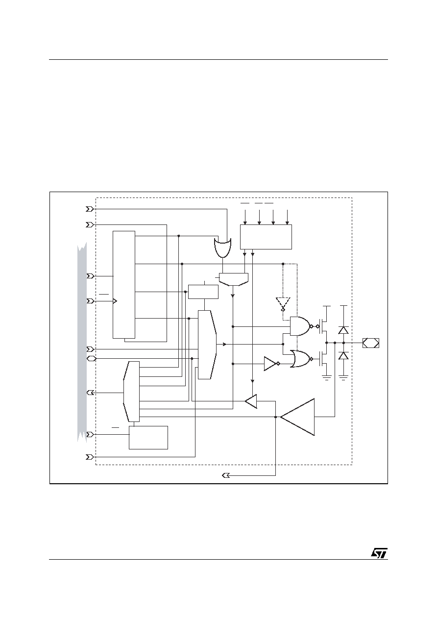
uPSD34xx - PSD MODULE
212/264
Individual Port Structures. Ports A, B, C, and D
have some differences. The structure of each indi-
vidual port is described in the next sections.
Port A Structure. Port A supports the following
operating modes:
MCU I/O Mode
GPLD Output Mode from Output Macrocells
MCELLABx
GPLD Input Mode to Input Macrocells IMCAx
Latched Address Output Mode
Peripheral I/O Mode
Port A also supports Open Drain/Slew Rate output
drive type options using csiop Drive Select regis-
ters. Pins PA0-PA3 can be configured to fast slew
rate, pins PA4-PA7 can be configured to Open
Drain Mode.
See Figure
85
for details.
Figure 85. Port A Structure
Note: 1. Port pins PA0-PA3 are capable of Fast Slew Rate output drive option. Port pins PA4-PA7 are capable of Open Drain output option.
I/O PORT A
LOGIC
O
U
T
P
U
T
M
U
X
P
D
B
M
U
X
DIRECTION
DRIVE SELECT
CONTROL
DATA OUT
(MCUI/O)
ENABLE OUT
DATA IN (MCUI/O)
D BIT, PERIPH I/O MODE
PT OUTPUT ENABLE (.OE)
LATCHED ADDR BIT
OE
MUX
OUTPUT
ENABLE
TYPICAL
PIN, PORT A
PSD MODULE RESET
ONE of 6
CSIOP
REGISTERS
OUTPUT
SELECT
PERIPHERAL I/O
MODE SETS
DIRECTION
8032 ADDRESS,
D
A
T
A
,
CONTR
OL B
U
S
1
2
3
4
1
2
3
4
5
6
FROM OMC OUTPUT (MCELLABx)
FROM PLD
INPUT BUS
FROM AND-
OR ARRAY
FROM OMC
ALLOCATOR
D
CLR
DIRECTION
DRIVE
CONTROL
(MCUI/O)
DATA OUT
8032
WR
RESET
PSDsoft
8032 RD
PSELx
WR
RD
PERIPH I/O
DATA BIT
TO IMCs
PIO EN
CSIOP
REGIS-
TERS
Q
Q
Q
Q
DRIVE TYPE SELECT
(1)
8032
DATA
BITS
8032
DATA
BIT
PIN INPUT
CMOS
BUFFER
NO
HYSTERESIS
V
DD
V
DD
PIN
OUTPUT
1 = OPEN
DRAIN,
PA4 - PA7
1 = FAST
SLEW RATE,
PA0 - PA3
IMCA0 - IMCA7
AI09179
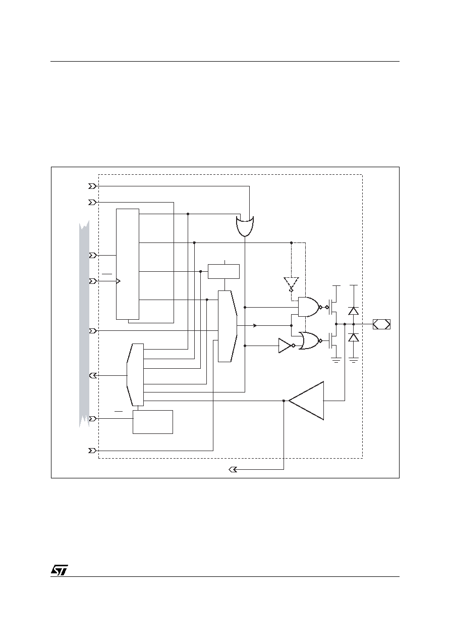
213/264
uPSD34xx - PSD MODULE
Port B Structure. Port B supports the following
operating modes:
MCU I/O Mode
GPLD Output Mode from Output Macrocells
MCELLABx, or MCELLBCx (OMC allocator
routes these signals)
GPLD Input Mode to Input Macrocells IMCBx
Latched Address Output Mode
Port B also supports Open Drain/Slew Rate output
drive type options using the csiop Drive Select reg-
isters. Pins PB0-PB3 can be configured to fast
slew rate, pins PB4-PB7 can be configured to
Open Drain Mode.
See Figure
86
for detail.
Figure 86. Port B Structure
Note: 1. Port pins PB0-PB3 are capable of Fast Slew Rate output drive option. Port pins PB4-PB7 are capable of Open Drain output option.
I/O PORT B
LOGIC
O
U
T
P
U
T
M
U
X
P
D
B
M
U
X
DIRECTION
DRIVE SELECT
CONTROL
DATA OUT
(MCUI/O)
ENABLE OUT
DATA IN (MCUI/O)
PT OUTPUT ENABLE (.OE)
LATCHED ADDR BIT
OUTPUT
ENABLE
OUTPUT
ENABLE
TYPICAL
PIN, PORT B
PSD MODULE RESET
ONE of 6
CSIOP
REGISTERS
OUTPUT
SELECT
8032 ADDRESS,
D
A
T
A
,
CONTR
OL B
U
S
1
2
3
1
2
3
4
5
6
FROM OMC OUTPUT
(MCELLABx or MCELLBCx)
FROM PLD
INPUT BUS
FROM AND-
OR ARRAY
FROM OMC
ALLOCATOR
D
CLR
DIRECTION
DRIVE
CONTROL
(MCUI/O)
DATA OUT
8032
WR
RESET
PSDsoft
8032 RD
TO IMCs
CSIOP
REGIS-
TERS
Q
Q
Q
Q
DRIVE TYPE SELECT
(1)
8032
DATA
BITS
8032
DATA
BIT
PIN INPUT
CMOS
BUFFER
NO
HYSTERESIS
V
DD
V
DD
PIN
OUTPUT
1 = OPEN
DRAIN,
PB4 - PB7
1 = FAST
SLEW RATE,
PB0 - PB3
IMCB0 - IMCB7
AI09180

uPSD34xx - PSD MODULE
214/264
Port C Structure. Port C supports the following
operating modes on pins PC2, PC3, PC4, PC7:
MCU I/O Mode
GPLD Output Mode from Output Macrocells
MCELLBC2, MCELLBC3, MCELLBC4,
MCELLBC7
GPLD Input Mode to Input Macrocells IMCC2,
IMCC3, IMCC4, IMCC7
See
Figure 87., page 215
for detail.
Port C pins can also be configured in PSDsoft for
other dedicated functions:
≠
Pins PC3 and PC4 support TSTAT and TERR
status indicators, to reduce the amount of time
required for JTAG ISP programming. These
two pins must be used together for this
function, adding to the four standard JTAG
signals. When TSTAT and TERR are used, it
is referred to as "6-pin JTAG". PC3 and PC4
cannot be used for other functions if they are
used for 6-pin JTAG. See
JTAG ISP and
JTAG Debug, page 226
for details.
≠
PC2 can be used as a voltage input (from
battery or other DC source) to backup the
contents of SRAM when V
DD
is lost. This
function is specified in PSDsoft Express as
SRAM Standby Mode (battery
backup), page 224
.
≠
PC3 can be used as an output to indicate
when a Flash memory program or erase
operation has completed. This is specified in
PSDsoft Express as
Ready/Busy
(PC3), page 184
.
≠
PC4 can be used as an output to indicate
when the SRAM has switched to backup
voltage (when V
DD
is less than the battery
input voltage on PC2). This is specified in
PSDsoft Express as "Standby-On Indicator"
(see
SRAM Standby Mode (battery
backup), page 224
).
The remaining four pins (TDI, TDO, TCK, TMS) on
Port C are dedicated to the JTAG function and
cannot be used for any other function. See
JTAG
ISP and JTAG Debug, page 226
.
Port C also supports the Open Drain output drive
type options on pins PC2, PC3, PC4, and PC7 us-
ing the csiop Drive Select registers.

215/264
uPSD34xx - PSD MODULE
Figure 87. Port C Structure
Note: 1. Pull-up switches to V
BAT
when SRAM goes to battery back-up mode.
2. Optional function on a specific Port C pin.
I/O PORT C
LOGIC
O
U
T
P
U
T
M
U
X
P
D
B
M
U
X
DIRECTION
DRIVE SELECT
DATA OUT
(MCUI/O)
ENABLE OUT
DATA IN (MCUI/O)
PT OUTPUT ENABLE, .OE (JTAG STATE MACHINE
AUTOMATICALLY CONTROLS OE FOR JTAG SIGNALS)
OUTPUT
ENABLE
TYPICAL
PIN,
PORT C
PSD MODULE RESET
ONE of 6
CSIOP
REGISTERS
8032 ADDRESS,
D
A
T
A
,
CONTR
OL B
U
S
1
2
3
4
5
1
2
3
4
5
FROM OMC OUTPUT (MCELLBCx)
STANDBY ON
(2)
FROM SRAM
BACK-UP CIRCUIT
FROM FLASH MEMORIES
TO/FROM JTAG
STATE MACHINE
FROM PLD
INPUT BUS
FROM AND-
OR ARRAY
FROM OMC
ALLOCATOR
D
CLR
DIRECTION
DRIVE
(MCUI/O)
DATA OUT
8032
WR
RESET
PSDsoft
8032 RD
TO IMCs
CSIOP
REGIS-
TERS
Q
Q
Q
DRIVE TYPE SELECT
(2)
8032
DATA
BITS
8032
DATA
BIT
PIN
INPUT
CMOS
BUFFER
NO
HYSTERESIS
V
DD
V
DD
/V
BAT
(1)
V
DD
/V
BAT
(1)
PIN
OUTPUT
50k
PULL-UP
ONLY ON
JTAG TDI,
TMS, TCK
SIGNALS
TO SRAM
BATTERY
BACK-UP
CIRCUIT
(2)
IMCC2, IMCC3,
IMCC4, IMCC7
RDY/BSY
(2)
TDO, TSTAT
(2)
, TERR
(2)
TDI, TMS, TCK
AI09181

uPSD34xx - PSD MODULE
216/264
Port D Structure. Port D has two I/O pins (PD1,
PD2) on 80-pin uPSD34xx devices, and just one
pin (PD1) on 52-pin devices, supporting the follow-
ing operating modes:
MCU I/O Mode
DPLD Output Mode for External Chip Selects,
ECS1, ECS2. This does not consume OMCs
in the GPLD.
PLD Input Mode ≠ direct input to the PLD Input
Bus available to DPLD and GPLD. Does not
use IMCs
See
Figure 88., page 217
for detail.
Port D pins can also be configured in PSDsoft as
pins for other dedicated functions:
≠
PD1 can be used as a common clock input to
all 16 OMC Flip-flops (see
OMCs, page 167
)
and also the
Automatic Power-Down
(APD), page 220
.
≠
PD2 can be used as a common chip select
signal (CSI) for the Flash and SRAM
memories on the PSD Module (see
Chip Se-
lect Input (CSI), page 222
). If driven to logic '1'
by an external source, CSI will force all
memories into standby mode regardless of
what other internal memory select signals are
doing on the PSD Module. This is specified in
PSDsoft as "PSD Chip Select Input, CSI".
Port D also supports the Fast Slew Rate output
drive type option using the csiop Drive Select reg-
isters.

217/264
uPSD34xx - PSD MODULE
Figure 88. Port D Structure
Note: 1. Optional function on a specific Port D pin.
I/O PORT D
LOGIC
O
U
T
P
U
T
M
U
X
P
D
B
M
U
X
DIRECTION
DRIVE SELECT
DATA OUT
(MCUI/O)
ENABLE OUT
DATA IN (MCUI/O)
PT OUTPUT ENABLE (.OE)
OUTPUT
ENABLE
OUTPUT
ENABLE
TYPICAL
PIN, PORT D
PSD MODULE RESET
ONE of 5
CSIOP
REGISTERS
8032 ADDRESS,
D
A
T
A
,
CONTR
OL B
U
S
1
2
1
2
3
4
5
FROM DPLD EXTERNAL CHIP (ECSx)
FROM PLD
INPUT BUS
FROM AND-
OR ARRAY
FROM DPLD
D
CLR
DIRECTION
DRIVE
(MCUI/O)
DATA OUT
8032
WR
RESET
PSDsoft
8032 RD
TO POWER MANAGEMENT AND PLD INPUT BUS
CSIOP
REGIS-
TERS
Q
Q
Q
DRIVE TYPE SELECT
8032
DATA
BITS
8032
DATA
BIT
PIN INPUT
CMOS
BUFFER
NO
HYSTERESIS
V
DD
V
DD
PIN
OUTPUT
1 = FAST
SLEW RATE
PD1. PIN, PD2.PIN
DIRECTLY TO PLD INPUT BUS, NO IMC
CSI
(1)
TO POWER MANAGEMENT
CLKIN
(1)
AI09182

uPSD34xx - PSD MODULE
218/264
Power Management. The PSD Module offers
configurable power saving options, and also a way
to manage power to the SRAM (battery backup).
These options may be used individually or in com-
binations. A top level description for these func-
tions is given here, then more detailed
descriptions will follow.
≠
Zero-Power Memory: All memory arrays
(Flash and SRAM) in the PSD Module are built
with zero-power technology, which puts the
memories into standby mode (~ zero DC
current) when 8032 address signals are not
changing. As soon as a transition occurs on
any address input, the affected memory
"wakes up", changes and latches its outputs,
then goes back to standby. The designer does
not have to do anything special to achieve this
memory standby mode when no inputs are
changing--it happens automatically. Thus,
the slower the 8032 clock, the lower the
current consumption.
Both PLDs (DPLD and GPLD) are also zero-
power, but this is not the default condition. The
8032 must set a bit in one of the csiop PMMR
registers at run-time to achieve zero-power.
≠
Automatic Power-Down (APD): The APD
feature allows the PSD Module to reach its
lowest current consumption levels. If enabled,
the APD counter will time-out when there is a
lack of 8032 bus activity for an extended
amount of time (8032 asleep). After time-out
occurs, all 8032 address and data buffers on
the PSD Module are shut down, preventing
the PSD Module memories and potentially the
PLDs from waking up from standby, even if
address inputs are changing state because of
noise or any external components driving the
address lines. Since the actual address and
data buffers are turned off, current
consumption is even further reduced.
Note: Non-address signals are still available
to PLD inputs and will wake up the PLDs if
these signals are changing state, but will not
wake up the memories.
The APD counter requires a relatively slow
external clock input on pin PD1 that does stop
when the 8032 goes to sleep mode.
≠
Forced Power-Down (FPD): The MCU can
put the PSD Module into Power-Down mode
with the same results as using APD described
above, but FPD does not rely on the APD
counter. Instead, FPD will force the PSD
Module into Power-Down mode when the
MCU firmware sets a bit in one of the csiop
PMMR registers. This is a good alternative to
APD because no external clock is needed for
the APD counter.
≠
PSD Module Chip Select Input (CSI): This
input on pin PD2 (80-pin devices only) can be
used to disable the internal memories, placing
them in standby mode even if address inputs
are changing. This feature does not block any
internal signals (the address and data buffers
are still on but signals are ignored) and CSI
does not disable the PLDs. This is a good
alternative to using the APD counter, which
requires an external clock on pin PD1.
≠
Non-Turbo Mode: The PLDs can operate in
Turbo or non-Turbo modes. Turbo mode has
the shortest signal propagation delay, but
consumes more current than non-Turbo
mode. A csiop register can be written by the
8032 to select modes, the default mode is with
Turbo mode enabled. In non-Turbo mode, the
PLDs can achieve very low standby current (~
zero DC current) while no PLD inputs are
changing, and the PLDs will even use less AC
current when inputs do change compared to
Turbo mode.
When the Turbo mode is enabled, there is a
significant DC current component AND the AC
current component is higher than non-Turbo
mode, as shown in
Figure 96., page 233
(5V)
and
Figure 97., page 233
(3.3V).
≠
Blocking Bits: Significant power savings can
be achieved by blocking 8032 bus control
signals (RD, WR, PSEN, ALE) from reaching
PLD inputs, if these signals are not used in
any PLD equations. Blocking is achieved by
the 8032 writing to the "blocking bits" in csiop
PMMR registers. Current consumption of the
PLDs is directly related to the composite
frequency of all transitions on PLD inputs, so
blocking certain PLD inputs can significantly
lower PLD operating frequency and power
consumption (resulting in a lower frequency
on the graphs of
Figure 96., page 233
and
Figure 97., page 233
).
≠
SRAM Backup Voltage: Pin PC2 can be
configured in PSDsoft to accept an alternate
DC voltage source (battery) to automatically
retain the contents of SRAM when V
DD
drops
below this alternate voltage.
Note: It is recommended to prevent unused
inputs from floating on Ports A, B, C, and D by
pulling them up to V
DD
with a weak external
resistor (100K
), or by setting the csiop
Direction register to "output" at run-time for all
unused inputs. This will prevent the CMOS
input buffers of unused input pins from
drawing excessive current.
The csiop PMMR register definitions are shown in
144
through
Table 146., page 219
.

219/264
uPSD34xx - PSD MODULE
Table 144. Power Management Mode Register PMMR0 (address = csiop + offset B0h)
Note: All the bits of this register are cleared to zero following Power-up. Subsequent Reset (RST) pulses do not clear the registers.
1. Blocking bits should be set to logic '1' only if the signal is not needed in a DPLD or GPLD logic equation.
Table 145. Power Management Mode Register PMMR2 (address = csiop + offset B4h)
Note: The bits of this register are cleared to zero following Power-up. Subsequent Reset (RST) pulses do not clear the registers.
1. Blocking bits should be set to logic '1' only if the signal is not needed in a DPLD or GPLD logic equation.
Table 146. Power Management Mode Register PMMR3 (address = csiop + offset C7h)
Note: The bits of this register are cleared to zero following Power-up. Subsequent Reset (RST) pulses do not clear the registers.
Bit 0
X
0
Not used, and should be set to zero.
Bit 1
APD Enable
0
Automatic Power Down (APD) counter is disabled.
1
APD counter is enabled
Bit 2
X
0
Not used, and should be set to zero.
Bit 3
PLD Turbo
Disable
0 = on PLD Turbo mode is on
1 = off PLD Turbo mode is off, saving power.
Bit 4
Blocking Bit,
CLKIN to
PLDs
(1)
0 = on
CLKIN (pin PD1) to the PLD Input Bus is not blocked. Every transition of CLKIN
powers-up the PLDs.
1 = off
CLKIN input to PLD Input Bus is blocked, saving power. But CLKIN still goes to APD
counter.
Bit 5
Blocking Bit,
CLKIN to
OMCs Only
(1)
0 = on CLKIN input is not blocked from reaching all OMCs' common clock inputs.
1 = off
CLKIN input to common clock of all OMCs is blocked, saving power. But CLKIN still
goes to APD counter and all PLD logic besides the common clock input on OMCs.
Bit 6
X
0
Not used, and should be set to zero.
Bit 7
X
0
Not used, and should be set to zero.
Bit 0
X
0
Not used, and should be set to zero.
Bit 1
X
0
Not used, and should be set to zero.
Bit 2
Blocking Bit,
WR to PLDs
(1)
0 = on 8032 WR input to the PLD Input Bus is not blocked.
1 = off 8032 WR input to PLD Input Bus is blocked, saving power.
Bit 3
Blocking Bit,
RD to PLDs
(1)
0 = on 8032 RD input to the PLD Input Bus is not blocked.
1 = off 8032 RD input to PLD Input Bus is blocked, saving power.
Bit 4
Blocking Bit,
PSEN to
PLDs
(1)
0 = on 8032 PSEN input to the PLD Input Bus is not blocked.
1 = off 8032 PSEN input to PLD Input Bus is blocked, saving power.
Bit 5
Blocking Bit,
ALE to
PLDs
(1)
0 = on 8032 ALE input to the PLD Input Bus is not blocked.
1 = off 8032 ALE input to PLD Input Bus is blocked, saving power.
Bit 5
Blocking Bit,
PC7 to
PLDs
(1)
0 = on Pin PC7 input to the PLD Input Bus is not blocked.
1 = off Pin PC7 input to PLD Input Bus is blocked, saving power.
Bit 7
X
0
Not used, and should be set to zero.
Bit 0
X
0
Not used, and should be set to zero.
Bit 1
FORCE_PD
0 = off APD counter will cause Power-Down Mode if APD is enabled.
1 = on Power-Down mode will be entered immediately regardless of APD activity.
Bit 3-7
X
0
Not used, and should be set to zero.

uPSD34xx - PSD MODULE
220/264
Automatic Power-Down (APD). The APD unit
shown in
Figure 74., page 188
puts the PSD Mod-
ule into power-down mode by monitoring the activ-
ity of the 8032 Address Latch Enable (ALE) signal.
If the APD unit is enabled by writing a logic '1' to
Bit 1 of the csiop PMMR0 register, and if ALE sig-
nal activity has stopped (8032 in sleep mode),
then the four-bit APD counter starts counting up. If
the ALE signal remains inactive for 15 clock peri-
ods of the CLKIN signal (pin PD1), then the APD
counter will reach maximum count and the power
down indicator signal (PDN) goes to logic '1' forc-
ing the PSD Module into power-down mode. Dur-
ing this time, all buffers on the PSD Module for
8032 address and data signals are disabled in sil-
icon, preventing the PSD Module memories from
waking up from stand-by mode, even if noise or
other devices are driving the address lines. The
PLDs will also stay in standby mode if the PLDs
are in non-Turbo mode and if all other PLD inputs
(non-address signals) are static.
However, if the ALE signal has a transition before
the APD counter reaches max count, the APD
counter is cleared to zero and the PDN signal will
not go active, preventing power-down mode. To
prevent unwanted APD time-outs during normal
8032 operation (not sleeping), it is important to
choose a clock frequency for CLKIN that will NOT
produce 15 or more pulses within the longest peri-
od between ALE transitions. A 32768 Hz clock sig-
nal is quite often an ideal frequency for CLKIN and
APD, and this frequency is often available on ex-
ternal supervisor or real-time clock devices.
The "PDN" power-down indicator signal is avail-
able to the PLD input bus to use in any PLD equa-
tions if desired. The user may want to send this
signal as a PLD output to an external device to in-
dicate the PSD Module is in power-down mode.
PSDsoft Express automatically includes the
"PDN" signal in the DPLD chip select equations for
FSx, CSBOOTx, RS0, and CSIOP.
The following should be kept in mind when the
PSD Module is in power-down mode:
≠
8032 address and data bus signals are
blocked from all memories and both PLDs.
≠
The PSD Module comes out of power-down
mode when: ALE starts pulsing again, or the
CSI input on pin PD2 transitions from logic '1'
to logic '0,' or the PSD Module reset signal,
RST, transitions from logic '0' to logic '1.'
≠
Various signals can be blocked (prior to
power-down mode) from entering the PLDs by
using "blocking bits" in csiop PMMR registers.
≠
All memories enter standby mode, and the
state of the PLDs and I/O Ports are
unchanged (if no PLD inputs change).
Table
148., page 225
shows the effects of power-
down mode on I/O pins while in various
operating modes.
≠
The 8032 Ports 1,3, and 4 on the MCU Module
are not affected at all by power-down mode in
the PSD Module.
≠
Power-down standby current given in the AC
specifications for PSD Module assume there
are no transitions on any unblocked PLD
input, and there are no output pins driving any
loads.
The APD counter will count whenever Bit 1 of
csiop PMMR0 register is set to logic '1,' and when
the ALE signal is steady at either logic '1' or logic
'0' (not transitioning).
Figure 90., page 222
shows
the flow leading up to power-down mode. The only
action required in PSDsoft Express to enable APD
mode is to select the pin function "Common Clock
Input, CLKIN" before programming with JTAG.

221/264
uPSD34xx - PSD MODULE
Forced Power Down (FDP). An alternative to
APD is FPD. The resulting power-savings is the
same, but the PDN signal in
Figure 89., page 222
is set and Power-Down mode is entered immedi-
ately when firmware sets the FORCE_PD Bit to
logic '1' in the csiop Register PMMR3 (Bit 1). FPD
will override APD counter activity when
FORCE_PD is set. No external clock source for
the APD counter is needed. The FORCE_PD Bit is
cleared only by a reset condition.
Caution must be used when implementing FPD
because code memory goes off-line as soon as
PSD Module Power-Down mode is entered, leav-
ing the MCU with no instruction stream to execute.
The MCU Module must put itself into Power-Down
mode after it puts the PSD Module into Power-
Down Mode. How can it do this if code memory
goes off-line? The answer is the Pre-Fetch Queue
(PFQ) in the MCU Module. By using the instruction
scheme shown in the 8051 assembly code exam-
ple in Table
147
, the PFQ will be loaded with the
final instructions to command the MCU Module to
Power Down mode after the PDS Module goes to
Power-Down mode. In this case, even though the
code memory goes off-line in the PSD Module, the
last few MCU instruction are sourced from the
PFQ.
Table 147. Forced Power-Down Example
PDOWN:
ANL
A8h, #7Fh
; disable all interrupts
ORL
9Dh, #C0h
; ensure PFQ and BC are enabled
MOV
DPTR, #xxC7
; load XDATA pointer to select PMMR3 register (xx = base
; address of csiop registers)
CLR
A
; clear A
JMP
LOOP
; first loop - fill PFQ/BQ with Power Down instructions
NOP
; second loop - fetch code from PFQ/BC and set Power-
; Down bits for PSD Module and then MCU Module
LOOP:
MOVX
@DPTR, A
; set FORCE_PD Bit in PMMR3 in PSD Module in second
; loop
MOV
87h, A
; set PD Bit in PCON Register in MCU Module in second
; loop
MOV
A, #02h
; set power-down bit in the A Register, but not in PMMR3 or
; PCON yet in first loop
JMP
LOOP
; uPSD enters into Power-Down mode in second loop

uPSD34xx - PSD MODULE
222/264
Figure 89. Automatic Power Down (APD) Unit
Figure 90. Power-Down Mode Flow Chart
Chip Select Input (CSI). Pin PD2 of Port D can
optionally be configured in PSDsoft Express as the
PSD Module Chip Select Input, CSI, which is an
active-low logic input. By default, pin PD2 does not
have the CSI function.
When the CSI function is specified in PSDsoft Ex-
press, the CSI signal is automatically included in
DPLD chip select equations for FSx, CSBOOTx,
RS0, and CSIOP. When the CSI pin is driven to
logic '0' from an external device, all of these mem-
ories will be available for READ and WRITE oper-
ations. When CSI is driven to logic '1,' none of
these memories are available for selection, re-
gardless of the address activity from the 8032, re-
ducing power consumption. The state of the PLD
and port I/O pins are not changed when CSI goes
to logic '1' (disabled).
PMMR0, BIT 1 (APD EN)
8032 ALE
PSD MODULE RST_
CSI (pin PD2)
CLKIN (pin PD1)
PDN
OMC OUTPUTS
FSx
CSBOOTx
RS0
CSIOP
8032 DATA FROM MCU MODULE
8032 ADDR FROM MCU MODULE
PDN
PDN
CSI
PMMR3, BIT 1 (FORCE_PD)
ENABLE
1 = FOUND
TRANSITION
1 = FOUND
EDGE
CLEAR
FULL
COUNT
DPLD CHIP
SELECT
EQUATIONS
GPLD
TRANSITION
DETECTION
EDGE
DETECTION
4-BIT APD
UP-COUNTER
ENABLE
CLK
1 = POWER
DOWN MODE
ENABLE
PSD
MODULE
LINE
BUFFERS
8032 DATA
8032 ADDR
WHEN CSI FUNCTION IS SPECIFIED IN PSDSOFT EXPRESS,
CSI IS PART OF EQUATIONS FOR FSx, CSBOOTx, RS0, and CSIOP
AI06608B
Enable APD.
Set PMMR0,
Bit 1 = 1
RESET
OPTIONAL. Disable desired inputs to
PLDs by setting PMMR0 bits 4 and 5,
and PMMR2 bits 2 through 6
ALE idle
for 15 CLKIN
clocks?
PDN = 1, PSD
Module in Power-
Down Mode
YES
NO
AI09183

223/264
uPSD34xx - PSD MODULE
PLD Non-Turbo Mode. The power consumption
and speed of the PLDs are controlled by the Turbo
Bit (Bit 3) in the csiop PMMR0 register. By setting
this bit to logic '1,' the Turbo mode is turned off and
both PLDs consume only stand-by current when
ALL PLD inputs have no transitions for an extend-
ed time (65ns for 5V devices, 100ns for 3.3 V de-
vices), significantly reducing current consumption.
The PLDs will latch their outputs and go to stand-
by, drawing very little current. When Turbo mode
is off, PLD propagation delay time is increased as
shown in the AC specifications for the PSD Mod-
ule. Since this additional propagation delay also
effects the DPLD, the response time of the memo-
ries on the PSD Module is also lengthened by that
same amount of time. If Turbo mode is off, the
user should add an additional wait state to the
8032 BUSCON SFR register if the 8032 clock fre-
quency is higher that a particular value. Please re-
fer to
Table 38., page 66
in the MCU Module
section.
The default state of the Turbo Bit is logic '0,' mean-
ing Turbo mode is on by default (after power-up
and reset conditions) until it is turned off by the
8032 writing to PMMR0.
PLD Current Consumption.
Figure
96., page 233
and
Figure 97., page 233
(5V and
3.3V devices respectively) show the relationship
between PLD current consumption and the com-
posite frequency of all the transitions on PLD in-
puts, indicating that a higher input frequency
results in higher current consumption.
Current consumption of the PLDs have a DC com-
ponent and an AC component. Both need to be
considered when calculating current consumption
for a specific PLD design. When Turbo mode is on,
there is a linear relationship between current and
frequency, and there is a substantial DC current
component consumed by the PSD Module when
there are no transitions on PLD inputs (composite
frequency is zero). The magnitude of this DC cur-
rent component is directly proportional to how
many product terms are used in the equations of
both PLDs. PSDsoft Express generates a "fitter"
report that specifies how many product terms were
used in a design out of a total of 186 available
product terms.
Figure 96., page 233
and
Figure
97., page 233
both give two examples, one with
100% of the 186 product terms used, and another
with 25% of the 186 product terms used.
Turbo Mode Current Consumption. To deter-
mine the AC current component of the specific
PLD design with Turbo mode on, the user will have
to interpolate from the graph, given the number of
product terms specified in the fitter report, and the
estimated composite frequency of PLD input sig-
nal transitions. For the DC component (y-axis
crossing), the user can calculate the number by
multiplying the number of product terms used
(from fitter report) times the DC current per prod-
uct term specified in the DC specifications for the
PSD Module. The total PLD current usage is the
sum of its AC and DC components.
Non-Turbo Mode Current Consumption. No-
tice in
Figure 96., page 233
and
Figure
97., page 233
that when Turbo mode is off, the DC
current consumption is "zero" (just standby cur-
rent) when the composite frequency of PLD input
transitions is zero (no input transitions). Now mov-
ing up the frequency axis to consider the AC cur-
rent component, current consumption remains
considerably less than Turbo mode until PLD input
transitions happen so rapidly that the PLDs do not
have time to latch their outputs and go to standby
between the transitions anymore. This is where
the lines converge on the graphs, and current con-
sumption becomes the same for PLD input transi-
tions at this frequency and higher regardless if
Turbo mode is on or off. To determine the current
consumption of the PLDs with Turbo mode off, ex-
trapolate the AC component from the graph based
on number of product terms and input frequency.
The only DC component in non-Turbo mode is the
PSD Module standby current.
The key to reducing PLD current consumption is to
reduce the composite frequency of transitions on
the PLD input bus, moving down the frequency
scale on the graphs. One way to do this is to care-
fully select which signals are entering PLD inputs,
not selecting high frequency signals if they are not
used in PLD equations. Another way is to use PLD
"Blocking Bits" to block certain signals from enter-
ing the PLD input bus.

uPSD34xx - PSD MODULE
224/264
PLD Blocking Bits. Blocking specific signals
from entering the PLDs using bits of the csiop
PMMR registers can further reduce PLD AC cur-
rent consumption by lowering the effective com-
posite frequency of inputs to the PLDs.
Blocking 8032 Bus Control Signals. When the
8032 is active on the MCU Module, four bus con-
trol signals (RD, WR, PSEN, and ALE) are con-
stantly transitioning to manage 8032 bus traffic.
Each time one of these signals has a transition
from logic '1' to '0,' or 0 to '1,' it will wake up the
PLDs if operating in non-Turbo mode, or when in
Turbo mode it will cause the affected PLD gates to
draw current. If equations in the DPLD or GPLD do
not use the signals RD, WR, PSEN, or ALE then
these signals can be blocked which will reduce the
AC current component substantially. These bus
control signals are rarely used in DPLD equations
because they are routed in silicon directly to the
memory arrays of the PSD Module, bypassing the
PLDs. For example, it is NOT necessary to qualify
a memory chip select signal with an MCU write
strobe, such as "fs0 = address range & !WR_".
Only "fs0 = address range" is needed.
Each of the 8032 bus control signals may be
blocked individually by writing to Bits 2, 3, 4, and 5
of the PMMR2 register shown in
Table
145., page 219
. Blocking any of these four bus
control signals only prevents them from reaching
the PLDs, but they will always go to the memories
directly.
However, sometimes it is necessary to use these
8032 bus control signals in the GPLD when creat-
ing interface signals to external I/O peripherals.
But it is still possible to save power by dynamically
unblocking the bus signals before reading/writing
the external device, then blocking the signals after
the communication is complete.
The user can also block an input signal coming
from pin PC7 to the PLD input bus if desired by
writing to Bit 6 of PMMR2.
Blocking Common Clock, CLKIN. The input
CLKIN (from pin PD1) can be blocked to reduce
current consumption. CLKIN is used as a common
clock input to all OMC flip-flips, it is a general input
to the PLD input bus, and it is used to clock the
APD counter. In PSDsoft Express, the function of
pin PD1 must be specified as "Common Clock In-
put, CLKIN" before programming the device with
JTAG to get the CLKIN function.
Bit 4 of PMMR0 can be set to logic '1' to block
CLKIN from reaching the PLD input bus, but
CLKIN will still reach the APD counter.
Bit 5 of PMMR0 can be set to logic '1' to block
CLKIN from reaching the OMC flip-flops only, but
CLKIN is still available to the PLD input bus and
the APD counter.
See
Table 144., page 219
for details.
SRAM Standby Mode (battery backup). The
SRAM on the PSD Module may optionally be
backed up by an external battery (or other DC
source) to make its contents non-volatile. This is
achieved by connecting a battery to pin PC2 on
Port C and selecting the "SRAM Standby" function
for pin PC2 within PSDsoft Express. Automatic
voltage supply cross-over circuitry is built into the
PSD Module to switch SRAM supply to battery as
soon as V
DD
drops below the voltage level of the
battery. SRAM contents are protected while bat-
tery voltage is greater than 2.0V. Pin PC4 on Port
C can be used as an output to indicate that a bat-
tery switch-over has occurred. This is configured
in PSDsoft Express by selecting the "Standby On
Indicator" option for pin PC4.
PSD Module Reset Conditions
The PSD Module receives a reset signal from the
MCU Module. This reset signal is referred to as the
"RST" input in PSD Module documentation, and it
is active-low when asserted. The character of the
RST signal generated from the MCU Module is de-
scribed in
SUPERVISORY
FUNCTIONS, page 67
.
Upon power-up, and while RST is asserted, the
PSD Module immediately loads its configuration
from non-volatile bits to configure the PLDs and
other items. PLD logic is operational and ready for
use well before RST is de-asserted. The state of
PLD outputs are determined by equations speci-
fied in PSDsoft Express.
The Flash memories are reset to Read Array
mode after any assertion of RST (even if a pro-
gram or erase operation is occurring).
Flash memory WRITE operations are automatical-
ly prevented while V
DD
is ramping up until it rises
above the V
LKO
voltage threshold at which time
Flash memory WRITE operations are allowed.
Once the uPSD34xx is up and running, any subse-
quent reset operation is referred to as a warm re-
set, until power is turned off again. Some PSD
Module functions are reset in different ways de-
pending if the reset condition was caused from a
power-up reset or a warm reset.
Table
148., page 225
summarizes how PSD Module
functions are affected by power-up and warm re-
sets, as well as the affect of PSD Module power-
down mode (from APD).
The I/O pins of PSD Module Ports A, B, C, and D
do not have weak internal pull-ups.
225/264
uPSD34xx - PSD MODULE
In MCU I/O mode, Latched Address Out mode,
and Peripheral I/O mode, the pins of Ports A, B, C,
and D become standard CMOS inputs during a re-
set condition. If no external devices are driving
these pins during reset, then these inputs may
float and draw excessive current. If low power con-
sumption is critical during reset, then these floating
inputs should be pulled up externally to V
DD
with a
weak (100K
minimum) resistor.
In PLD I/O mode, pins of Ports A, B, C, and D may
also float during reset if no external device is driv-
ing them, and if there is no equation specified for
the DPLD or GPLD to make them an output. In this
case, a weak external pull-up resistor (100K
min-
imum) should be used on floating pins to avoid ex-
cessive current draw.
The pins on Ports 1, 3, and 4 of the 8032 MCU
module do have weak internal pull-ups and the in-
puts will not float, so no external pull-ups are need-
ed.
Table 148. Function Status During Power-Up Reset, Warm Reset, Power-down Mode
Note: 1. VM register Bit 7 (PIO_EN) and Bit 0 (SRAM in 8032 program space) are cleared to zero at power-up and warm reset conditions.
Port Configuration
Power-Up Reset
Warm Reset
APD Power-down Mode
MCU I/O
Pins are in input mode
Pins are in input mode
Pin logic state is
unchanged
PLD I/O
Pin logic is valid after
internal PSD Module
configuration bits are
loaded. Happens long
before RST is de-asserted
Pin logic is valid and is
determined by PLD logic
equations
Pin logic depends on inputs
to PLD (8032 addresses
are blocked from reaching
PLD inputs during power-
down mode)
Latched Address Out Mode
Pins are High Impedance
Pins are High Impedance
Pins logic state not defined
since 8032 address signals
are blocked
Peripheral I/O Mode
Pins are High Impedance
Pins are High Impedance
Pins are High Impedance
JTAG ISP and Debug
JTAG channel is active and
available
JTAG channel is active and
available
JTAG channel is active and
available
Register
Power-Up Reset
Warm Reset
APD Power-down Mode
PMMR0 and PMMR2
Cleared to 00h
Unchanged
Unchanged
Output of OMC Flip-flops
Cleared to '0'
Depends on .re and .pr
equations
Depends on .re and .pr
equations
VM Register
(1)
Initialized with value that
was specified in PSDsoft
Initialized with value that
was specified in PSDsoft
Unchanged
All other csiop registers
Cleared to 00h
Cleared to 00h
Unchanged
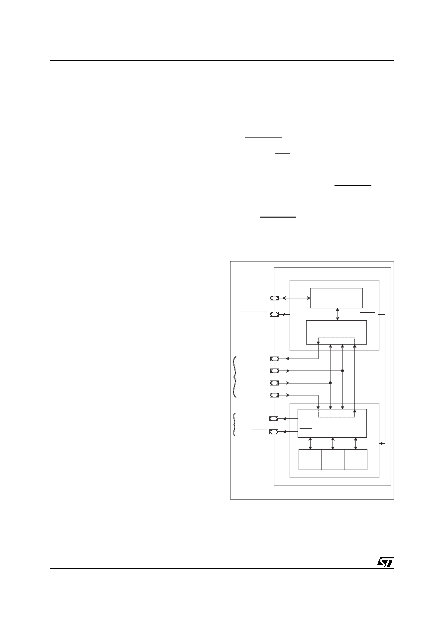
uPSD34xx - PSD MODULE
226/264
JTAG ISP and JTAG Debug. An IEEE 1149.1
serial JTAG interface is used on uPSD34xx devic-
es for ISP (In-System Programming) of the PSD
module, and also for debugging firmware on the
MCU Module. IEEE 1149.1 Boundary Scan oper-
ations are not supported in the uPSD34xx.
The main advantage of JTAG ISP is that a blank
uPSD34xx device may be soldered to a circuit
board and programmed with no involvement of the
8032, meaning that no 8032 firmware needs to be
present for ISP. This is good for manufacturing, for
field updates, and for easy code development in
the lab. JTAG-based programmers and debug-
gers for uPSD34xx are available from STMicro-
electronics and 3rd party vendors.
ISP is different than IAP (In-Application Program-
ming). IAP involves the 8032 to program Flash
memory over any interface supported by the 8032
(e.g., UART, SPI, I2C), which is good for remote
updates over a communication channel.
uPSD34xx devices support both ISP and IAP. The
entire PSD Module (Flash memory and PLD) may
be programmed with JTAG ISP, but only the Flash
memories may be programmed using IAP.
JTAG Chaining Inside the Package. JTAG pro-
tocol allows serial "chaining" of more than one de-
vice in a JTAG chain. The uPSD34xx is
assembled with a stacked die process combining
the PSD Module (one die) and the MCU Module
(the other die). These two die are chained together
within the uPSD34xx package. The standard
JTAG interface has four basic signals:
TDI - Serial data into device
TDO - Serial data out of device
TCK - Common clock
TMS - Mode Selection
Every device that supports IEEE 1149.1 JTAG
communication contains a Test Access Port (TAP)
controller, which is a small state machine to man-
age JTAG protocol and serial streams of com-
mands and data. Both the PSD Module and the
MCU Module each contain a TAP controller.
Figure
91
illustrates how these die are chained
within a package. JTAG programming/test equip-
ment will connect externally to the four IEEE
1149.1 JTAG pins on Port C. The TDI pin on the
uPSD34xx package goes directly to the PSD Mod-
ule first, then exits the PSD Module through TDO.
TDO of the PSD Module is connected to TDI of the
MCU Module. The serial path is completed when
TDO of the MCU Module exits the uPSD34xx
package through the TDO pin on Port C. The
JTAG signals TCK and TMS are common to both
modules as specified in IEEE 1149.1. When JTAG
devices are chained, typically one devices is in
BYPASS mode while another device is executing
a JTAG operation. For the uPSD34xx, the PSD
Module is in BYPASS mode while debugging the
MCU Module, and the MCU Module is in BYPASS
mode while performing ISP on the PSD Module.
The RESET_IN input pin on the uPSD34xx pack-
age goes to the MCU Module, and this module will
generate the RST reset signal for the PSD Mod-
ule. These reset signals are totally independent of
the JTAG TAP controllers, meaning that the JTAG
channel is operational when the modules are held
in reset. It is required to assert RESET_IN during
ISP. STMicroelectronics and 3rd party JTAG ISP
tools will automatically assert a reset signal during
ISP. However, the user must connect this reset
signal to RESET_IN as shown in examples in Fig-
ure
Figure 92., page 227
and
Figure
93., page 229
.
Figure 91. JTAG Chain in uPSD34xx Package
JTAG TDI
JTAG TMS
JTAG TCK
JTAG TDO
TDI
TMS TCK
TDO
TDO
TMS TCK
TDI
PC3 / TSTAT
PC4 / TERR
TSTAT
TERR
OPTIONAL
JTAG TAP
CONTROLLER
JTAG TAP
CONTROLLER
RESET_IN
OPTIONAL
DEBUG
RESET
RST
8032 MCU
MCU MODULE
PSD MODULE
MAIN
FLASH
MEMORY
2ND
FLASH
MEMORY
PLD
uPSD34xx
IEEE 1149.1
AI10460
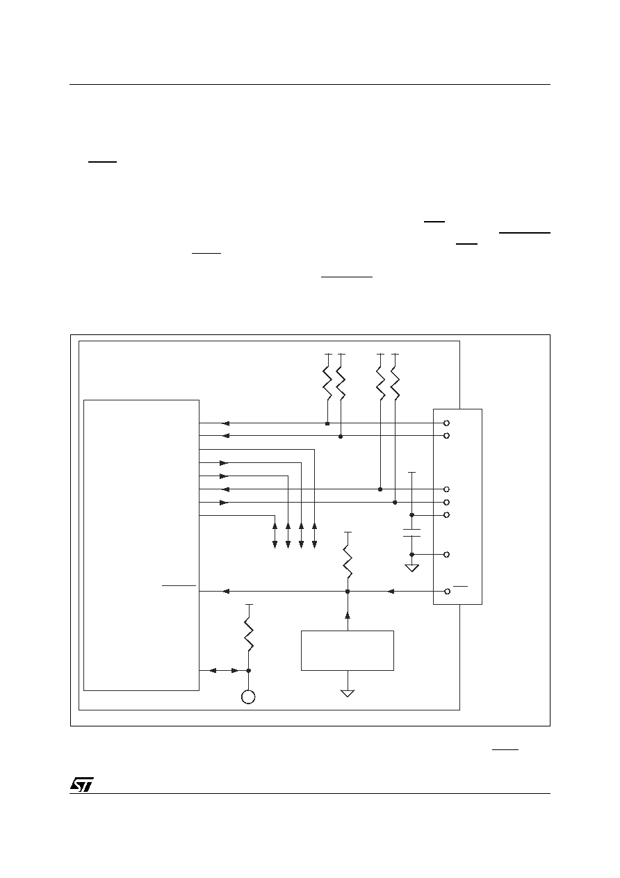
227/264
uPSD34xx - PSD MODULE
In-System Programming. The ISP function can
use two different configurations of the JTAG inter-
face:
4-pin JTAG: TDI, TDO, TCK, TMS
6-pin JTAG: Signals above plus TSTAT,
TERR
At power-up, the four basic JTAG signals are all in-
puts, waiting for a command to appear on the
JTAG bus from programming or test equipment.
When the enabling command is received, TDO be-
comes an output and the JTAG channel is fully
functional. The same command that enables the
JTAG channel may optionally enable the two addi-
tional signals, TSTAT and TERR.
4-pin JTAG ISP (default).
The four basic JTAG
pins on Port C are enabled for JTAG operation at
all times. These pins may not be used for other I/
O functions. There is no action needed in PSDsoft
Express to configure a device to use 4-pin JTAG,
as this is the default condition. No 8032 firmware
is needed to use 4-pin ISP because all ISP func-
tions are controlled from the external JTAG pro-
gram/test equipment. Figure
92
shows
recommended connections on a circuit board to a
JTAG program/test tool using 4-pin JTAG. It is re-
quired to connect the RST output signal from the
JTAG program/test equipment to the RESET_IN
input on the uPSD34xx. The RST signal is driven
by the equipment with an Open Drain driver, allow-
ing other sources (like a push button) to drive
RESET_IN without conflict.
Note: The recommended pull-up resistors and de-
coupling capacitor are illustrated in Figure
92
.
Figure 92. Recommended 4-pin JTAG Connections
Note: 1. For 5V uPSD34xx devices, pull-up resistors and V
CC
pin on the JTAG connector should be connected to 5V system V
DD
.
2. For 3.3V uPSD34xx devices, pull-up resistors and V
CC
pin on the JTAG connector should be connected to 3.3V system V
CC
.
3. This signal is driven by an Open-Drain output in the JTAG equipment, allowing more than one source to activate RESETIN.
TMS - PC0
TCK - PC1
SRAM STBY or I/O - PC2
GENERAL I/O - PC3
GENERAL I/O - PC4
TDI - PC5
TDO - PC6
GENERAL I/O - PC7
JTAG
CONN.
100k
typical
TMS
TCK
TDI
TDO
GENERAL I/O
SIGNALS
GND
V
CC
(1,2)
RST
(3)
uPSD34xx
0.01
µF
CIRCUIT
BOARD
JTAG
Programming
or Test
Equipment
Connects Here
10k
PUSH BUTTON
or ANY OTHER
RESET SOURCE
DEBUG
OPTIONAL
TEST POINT
100k
RESETIN
AI10457

uPSD34xx - PSD MODULE
228/264
6-pin JTAG ISP (optional). The optional signals
TSTAT and TERR are programming status flags
that can reduce programming time by as much as
30% compared to 4-pin JTAG because this status
information does not have to be scanned out of the
device serially. TSTAT and TERR must be used
as a pair for 6-pin JTAG operation.
≠
TSTAT (pin PC3) indicates when
programming of a single Flash location is
complete. Logic 1 = Ready, Logic 0 = busy.
≠
TERR (pin PC4) indicates if there was a Flash
programming error. Logic 1 = no error,
Logic 0 = error.
The pin functions for PC3 and PC4 must be select-
ed as "Dedicated JTAG - TSTAT" and "Dedicated
JTAG - TERR" in PSDsoft Express to enable 6-pin
JTAG ISP.
No 8032 firmware is needed to use 6-pin ISP be-
cause all ISP functions are controlled from the ex-
ternal JTAG program/test equipment.
TSTAT and TERR are functional only when JTAG
ISP operations are occurring, which means they
are non-functional during JTAG debugging of the
8032 on the MCU Module.
Programming times vary depending on the num-
ber of locations to be programmed and the JTAG
programming equipment, but typical JTAG ISP
programming times are 10 to 25 seconds using 6-
pin JTAG. The signals TSTAT and TERR are not
included in the IEEE 1149.1 specification.
Figure 93., page 229
shows recommended con-
nections on a circuit board to a JTAG program/test
tool using 6-pin JTAG. It is required to connect the
RST output signal from the JTAG program/test
equipment to the RESET_IN input on the
uPSD34xx. The RST signal is driven by the equip-
ment with an Open Drain driver, allowing other
sources (like a push button) to drive RESET_IN
without conflict.
Note: The recommended pull-up resistors and de-
coupling capacitor are illustrated in Figure
93
.

229/264
uPSD34xx - PSD MODULE
Figure 93. Recommended 6-pin JTAG Connections
Note: 1. For 5V uPSD34xx devices, pull-up resistors and V
CC
pin on the JTAG connector should be connected to 5V system V
DD
.
2. For 3.3V uPSD34xx devices, pull-up resistors and V
CC
pin on the JTAG connector should be connected to 3.3V system V
CC
.
3. This signal is driven by an Open-Drain output in the JTAG equipment, allowing more than one source to activate RESET_IN.
TMS - PC0
TCK - PC1
SRAM STBY or I/O - PC2
TSTAT - PC3
TERR - PC4
TDI - PC5
TDO - PC6
GENERAL I/O - PC7
JTAG
CONN.
100k typical
TMS
TCK
TDI
TERR
TSTAT
TDO
GENERAL I/O
SIGNALS
GND
V
CC
(1,2)
RST
(3)
uPSD34xx
0.01
µF
CIRCUIT
BOARD
JTAG
Programming
or Test
Equipment
Connects Here
10k
PUSH BUTTON
or ANY OTHER
RESET SOURCE
DEBUG
OPTIONAL
TEST POINT
100k
RESETIN
AI10458
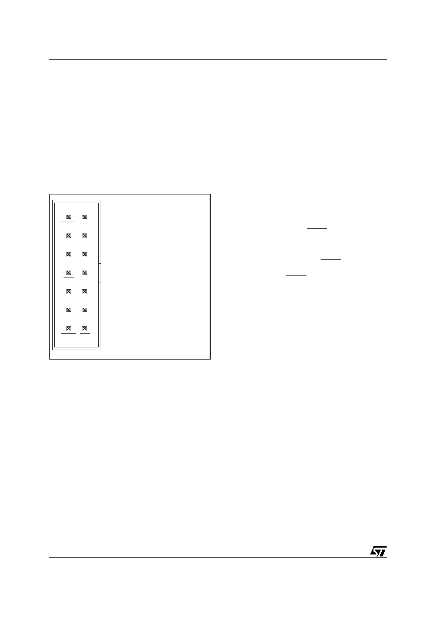
uPSD34xx - PSD MODULE
230/264
Recommended JTAG Connector. There is no
industry standard JTAG connector. STMicroelec-
tronics recommends a specific JTAG connector
and pinout for uPSD3xxx so programming and de-
bug equipment will easily connect to the circuit
board. The user does not have to use this connec-
tor if there is a different connection scheme.
The recommended connector scheme can accept
a standard 14-pin ribbon cable connector (2 rows
of 7 pins on 0.1" centers, 0.025" square posts,
standard keying) as shown in Figure
94
. See the
STMicroelectronics "FlashLINK, FL-101 User
Manual" for more information.
Figure 94. Recommended JTAG Connector
Chaining uPSD34xx Devices. It is possible to
chain a uPSD34xx device with other uPSD34xx
devices on a circuit board, and also chain with
IEEE 1149.1 compliant devices from other manu-
facturers.
Figure 95., page 231
shows a chaining
example. The TDO of one device connects to the
TDI of the next device, and so on. Only one device
is performing JTAG operations at any given time
while the other two devices are in BYPASS mode.
Configuration for JTAG chaining can be made in
PSDsoft Express by choosing "More than one de-
vice" when prompted about chaining devices. No-
tice in
Figure 95., page 231
that the uPSD34xx
devices are chained externally, but also be aware
that the two die within each uPSD34xx device are
chained internally. This internal chaining of die is
transparent to the user and is taken care of by PS-
Dsoft Express and 3rd party JTAG tool software.
The example in
Figure 95., page 231
also shows
how to use 6-pin JTAG when chaining devices.
The signals TSTAT and TERR are configured as
open-drain type signals from PSDsoft Express.
This facilitates a wired-OR connection of TSTAT
signals from multiple uPSD34xx devices and also
a wired-OR connection of TERR signals from
those same multiple devices. PSDsoft Express
puts TSTAT and TERR signals into open-drain
mode by default, requiring external pull-up resis-
tors. Click on 'Properties' in the JTAG-ISP window
of PSDsoft Express to change to standard CMOS
push-pull outputs if desired, but wired-OR logic is
not possible in CMOS output mode.
TDO
TCK
TMS
V
CC
TDI
GND
JEN
TERR
GND
GND
RST
TSTAT
CNTL
TRST
14
12
10
13
11
9
7
8
6
5
4
3
2
1
KEY
WAY
VIEW: Looking into face of shrouded
male connector, with 0.025"
posts on 0.1" centers.
Connector reference:
Molex 70247-1401
This connector accepts a 14-pin
ribbon cable such as:
∑ Samtec:
HCSD-07-D-06.00-01-S-N
∑ Digikey:
M3CCK-14065-ND
AI09187
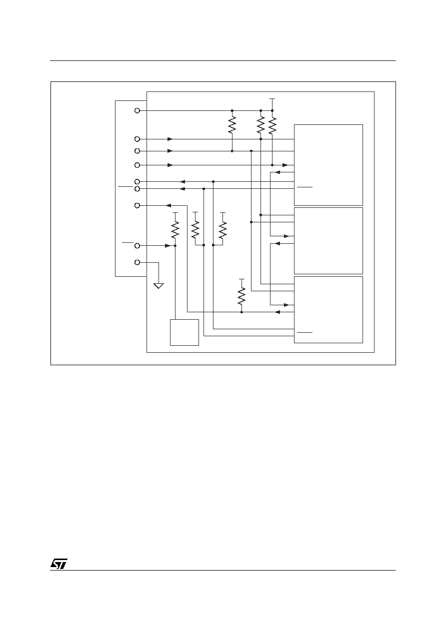
231/264
uPSD34xx - PSD MODULE
Figure 95. Example of Chaining uPSD34xx Devices
Device 1
µPSD34xx
uPSD34xx
TMS
TCK
TDI
TDO
IEEE 1149.1
Compliant
Device
Device 2
Device N
System
Reset
Circuitry
TMS
TCK
TDI
TDO
TSTAT
TERR
CIRCUIT BOARD
JTAG
CONN.
V
CC
TMS
TCK
TDI
TSTAT
TERR
TDO
RST
GND
100K
100K
100K
100K
100K
10K
100K
JTAG
Programming
or Test
Equipment
Connects Here
Optional
Optional
TMS
TCK
TDI
TDO
TSTAT
TERR
AI10459

uPSD34xx - PSD MODULE
232/264
Debugging the 8032 MCU Module. The 8032
on the MCU module may be debugged in-circuit
using the same four basic JTAG signals as used
for JTAG ISP (TDI, TDO, TCK, TMS). The signals
TSTAT and TERR are not needed for debugging,
and they will not create a problem if they exist on
the circuit board while debugging. The same con-
nector specified in
Figure 94., page 230
can be
used for ISP or for 8032 debugging. There are 3rd
party suppliers of uPSD34xx JTAG debugging
equipment (check www.st.com/psm). These are
small pods which connect to a PC (or notebook
computer) using a USB interface, and they are
driven by an 8032 Integrated Development Envi-
ronment (IDE) running on the PC.
Standard debugging features are provided
through this JTAG interface such as single-step,
breakpoints, trace, memory dump and fill, and oth-
ers. There is also a dedicated Debug pin (shown
in
Figure 91., page 226
) which can be configured
as an output to trigger external devices upon a
programmable internal event (e.g., breakpoint
match), or the pin can be configured as an input so
an external device can initiate an internal debug
event (e.g., break execution). The Debug pin func-
tion is configured by the 8032 IDE debug software
tool. See
DEBUG UNIT, page 40
for more details.
The Debug signal should always be pulled up ex-
ternally with a weak pull-up (100K minimum) to
V
CC
even if nothing is connected to it, as shown in
Figure 92., page 227
and
Figure 93., page 229
.
JTAG Security Setting. A programmable securi-
ty bit in the PSD Module protects its contents from
unauthorized viewing and copying. The security
bit is set by clicking on the "Additional PSD Set-
tings" box in the main flow diagram of PSDsoft Ex-
press, then choosing to set the security bit. Once
a file with this setting is programmed into a
uPSD34xx using JTAG ISP, any further attempts
to communicate with the uPSD34xx using JTAG
will be limited. Once secured, the only JTAG oper-
ation allowed is a full-chip erase. No reading or
modifying Flash memory or PLD logic is allowed.
Debugging operations to the MCU Module are
also not allowed. The only way to defeat the secu-
rity bit is to perform a JTAG ISP full-chip erase op-
eration, after which the device is blank and may be
used again. The 8032 on the MCU Module will al-
ways have access to PSM Module memory con-
tents through the 8-bit 8032 data bus connecting
the two die, even while the security bit is set.
Initial Delivery State. When delivered from ST-
Microelectronics, uPSD34xx devices are erased,
meaning all Flash memory and PLD configuration
bits are logic '1.' Firmware and PLD logic configu-
ration must be programmed at least the first time
using JTAG ISP. Subsequent programming of
Flash memory may be performed using JTAG ISP,
JTAG debugging, or the 8032 may run firmware to
program Flash memory (IAP).
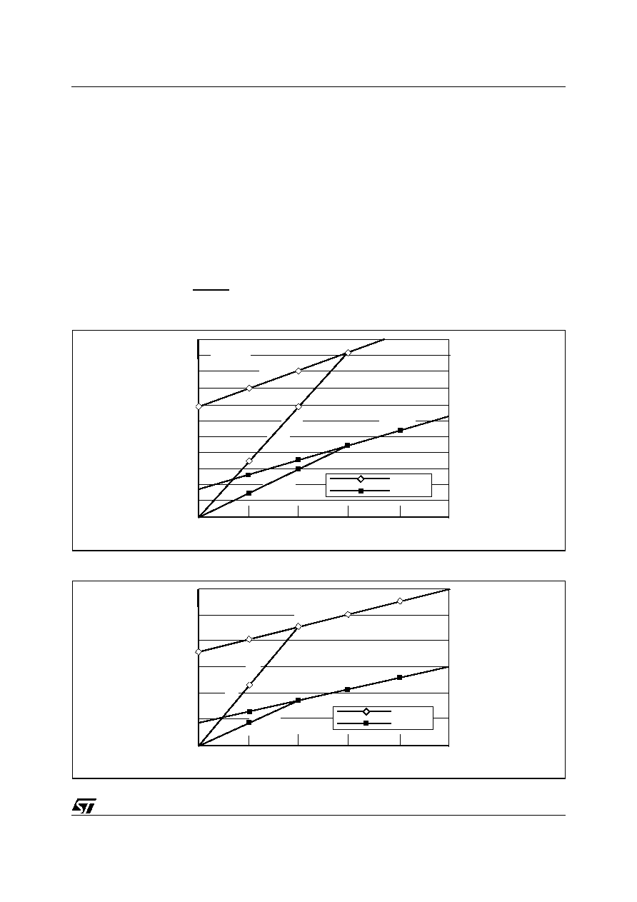
233/264
uPSD34xx - AC/DC PARAMETERS
AC/DC PARAMETERS
These tables describe the AD and DC parameters
of the uPSD34xx Devices:
DC Electrical Specification
AC Timing Specification
PLD Timing
≠
Combinatorial Timing
≠
Synchronous Clock Mode
≠
Asynchronous Clock Mode
≠
Input Macrocell Timing
MCU Module Timing
≠
READ Timing
≠
WRITE Timing
≠
Power-down and RESET Timing
The following are issues concerning the parame-
ters presented:
≠
In the DC specification the supply current is
given for different modes of operation.
≠
The AC power component gives the PLD,
Flash memory, and SRAM mA/MHz
specification. Figure
96
and Figure
97
show
the PLD mA/MHz as a function of the number
of Product Terms (PT) used.
≠
In the PLD timing parameters, add the
required delay when Turbo Bit is '0.'
Figure 96. PLD I
CC
/Frequency Consumption (5V range)
Figure 97. PLD I
CC
/Frequency Consumption (3V range)
0
10
20
30
40
60
70
80
90
100
110
V
CC
= 5V
50
0
10
15
5
20 25
HIGHEST COMPOSITE FREQUENCY AT PLD INPUTS (MHz)
I
CC
≠ (mA)
TURBO ON (100%)
TURBO ON (25%)
TURBO OFF
TURBO OFF
PT 100%
PT 25%
AI02894
0
10
20
30
40
50
60
V
CC
= 3V
0
10
15
5
20 25
I
CC
≠ (mA)
TURBO ON (100%)
TURBO ON (25%)
TURBO OFF
TURBO OFF
HIGHEST COMPOSITE FREQUENCY AT PLD INPUTS (MHz)
PT 100%
PT 25%
AI03100
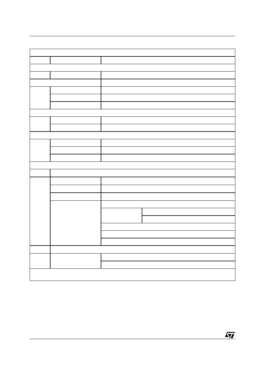
uPSD34xx - AC/DC PARAMETERS
234/264
Table 149. PSD Module Example, Typ. Power Calculation at V
CC
= 5.0V (Turbo Mode Off)
Conditions
MCU Clock Frequency
= 12MHz
Highest Composite PLD input frequency
(Freq PLD)
= 8MHz
MCU ALE frequency (Freq ALE)
= 2MHz
% Flash memory Access
= 80%
% SRAM access
= 15%
% I/O access
= 5% (no additional power above base)
Operational Modes
% Normal
= 40%
% Power-down Mode
= 60%
Number of product terms used
(from fitter report)
= 45 PT
% of total product terms
= 45/182 = 24.7%
Turbo Mode
= Off
Calculation (using typical values)
I
CC
total
= I
CC
(MCUactive) x %MCUactive + I
CC
(PSDactive) x %PSDactive + I
PD
(pwrdown) x %pwrdown
I
CC
(MCUactive)
= 20mA
I
PD
(pwrdown)
= 250uA
I
CC
(PSDactive)
= I
CC
(ac) + I
CC
(dc)
= %flash x 2.5mA/MHz x Freq ALE
+ %SRAM x 1.5mA/MHz x Freq ALE
+ % PLD x (from graph using Freq PLD)
= 0.8 x 2.5mA/MHz x 2MHz + 0.15 x 1.5mA/MHz x 2MHz + 24mA
= (4 + 0.45 + 24) mA
= 28.45mA
I
CC
total
= 20mA x 40% + 28.45mA x 40% + 250uA x 60%
= 8mA + 11.38mA + 150uA
= 19.53mA
This is the operating power with no Flash memory Erase or Program cycles in progress. Calculation is based on all I/O
pins being disconnected and I
OUT
= 0mA.
235/264
uPSD34xx - MAXIMUM RATING
MAXIMUM RATING
Stressing the device above the rating listed in the
Absolute Maximum Ratings" table may cause per-
manent damage to the device. These are stress
ratings only and operation of the device at these or
any other conditions above those indicated in the
Operating sections of this specification is not im-
plied. Exposure to Absolute Maximum Rating con-
ditions for extended periods may affect device
reliability. Refer also to the STMicroelectronics
SURE Program and other relevant quality docu-
ments.
Table 150. Absolute Maximum Ratings
Note: 1. IPC/JEDEC J-STD-020A
2. JEDEC Std JESD22-A114A (C1=100pF, R1=1500
, R2=500 )
DC AND AC PARAMETERS
This section summarizes the operating and mea-
surement conditions, and the DC and AC charac-
teristics of the device. The parameters in the DC
and AC Characteristic tables that follow are de-
rived from tests performed under the Measure-
ment Conditions summarized in the relevant
tables. Designers should check that the operating
conditions in their circuit match the measurement
conditions when relying on the quoted parame-
ters.
Table 151. Operating Conditions (5V Devices)
Table 152. Operating Conditions (3.3V Devices)
Symbol
Parameter
Min.
Max.
Unit
T
STG
Storage Temperature
≠65
125
∞C
T
LEAD
Lead Temperature during Soldering (20 seconds max.)
(1)
235
∞C
V
IO
Input and Output Voltage (Q = V
OH
or Hi-Z)
≠0.5
6.5
V
V
CC
Supply Voltage
≠0.5
6.5
V
V
PP
Device Programmer Supply Voltage
≠0.5
14.0
V
V
ESD
Electrostatic Discharge Voltage (Human Body Model)
(2)
≠2000
2000
V
Symbol
Parameter
Min.
Max.
Unit
V
CC
Supply Voltage
4.5
5.5
V
T
A
Ambient Operating Temperature (industrial)
≠40
85
∞C
Ambient Operating Temperature (commercial)
0
70
∞C
Symbol
Parameter
Min.
Max.
Unit
V
CC
Supply Voltage
3.0
3.6
V
T
A
Ambient Operating Temperature (industrial)
≠40
85
∞C
Ambient Operating Temperature (commercial)
0
70
∞C
uPSD34xx - DC AND AC PARAMETERS
236/264
Table 153. AC Signal Letters for Timing
Note: Example: t
AVLX
= Time from Address Valid to ALE Invalid.
Table 154. AC Signal Behavior Symbols for
Timing
Note: Example: t
AVLX
= Time from Address Valid to ALE Invalid.
Figure 98. Switching Waveforms ≠ Key
A
Address
C
Clock
D
Input Data
I
Instruction
L
ALE
N
RESET Input or Output
P
PSEN signal
Q
Output Data
R
RD signal
W
WR signal
B
V
STBY
Output
M
Output Macrocell
t
Time
L
Logic Level Low or ALE
H
Logic Level High
V
Valid
X
No Longer a Valid Logic Level
Z
Float
PW
Pulse Width
WAVEFORMS
INPUTS
OUTPUTS
STEADY INPUT
MAY CHANGE FROM
HI TO LO
MAY CHANGE FROM
LO TO HI
DON'T CARE
OUTPUTS ONLY
STEADY OUTPUT
WILL BE CHANGING
FROM HI TO LO
WILL BE CHANGING
LO TO HI
CHANGING, STATE
UNKNOWN
CENTER LINE IS
TRI-STATE
AI03102

237/264
uPSD34xx - DC AND AC PARAMETERS
Table 155. Major Parameters
Note: 1. Operating current is measured while the uPSD34xx is executing a typical program at 40MHz.
Parameter
Test Conditions/Comments
5.0V Value
3.3V Value
Unit
Operating Voltage
≠
4.5 to 5.5 (PSD);
3.0 to 3.6 (MCU)
3.0 to 3.6
(PSD and MCU)
V
Operating Temperature
≠
≠40 to 85
≠40 to 85
∞C
MCU Frequency
8MHz (min) for I
2
C
3 Min, 40 Max
3 Min, 40 Max
MHz
Operating Current, Typical
(1)
(20% of PLD used; 25∞C
operation. Bus control signals are
blocked from the PLD in Non-
Turbo mode.)
40MHz Crystal, Turbo
79
63
mA
40MHz Crystal, Non-Turbo
71
58
mA
8MHz Crystal, Turbo
32
24
mA
8MHz Crystal, Non-Turbo
17.7
14
mA
Idle Current, Typical
(20% of PLD used; 25∞C
operation)
40MHz Crystal divided by 2048
internally.
All interfaces are disabled.
19
18
mA
Standby Current, Typical
Power-down Mode
needs reset to exit.
140
120
µA
SRAM Backup Current, Typical
If external battery is attached.
0.5
0.5
µA
I/O Sink/Source Current,
Ports A, B, C, and D
V
OL
= 0.45V (max);
V
OH
= 2.4V (min)
I
OL
= 8 (max);
I
OH
= ≠2 (min)
I
OL
= 4 (max);
I
OH
= ≠1 (min)
mA
I/O Sink/Source Current,
Port 4
V
OL
= 0.6V (max);
V
OH
= 2.4V (min)
I
OL
= 10 (max);
I
OH
= ≠10 (min)
I
OL
= 10 (max);
I
OH
= ≠10 (min)
mA
PLD Macrocells
For registered or
combinatorial logic
16
16
≠
PLD Inputs
Inputs from pins, feedback,
or MCU addresses
69
69
≠
PLD Outputs
Output to pins or
internal feedback
18
18
≠
PLD Propagation Delay, Typical,
Turbo Mode
PLD input to output
15
22
ns
uPSD34xx - DC AND AC PARAMETERS
238/264
Table 156. Preliminary MCU Module DC Characteristics
Note: 1. Power supply (V
CC
) is always 3.0 to 3.6V for the MCU Module. V
DD
for the PSD Module may be 3V or 5V.
2. Port 1 is not 5V tolerant; maximum V
IH
= V
CC
+ 0.5.
3. I
PD
(Power-down Mode) is measured with: XTAL1 = V
SS
; XTAL2 = NC; RESET = V
CC
; Port 0 = V
CC
; all other pins are disconnected.
4. I
CC-CPU
(Active Mode) is measured with: XTAL1 driven with t
CLCH
, t
CHCL
= 5ns, V
IL
= V
SS
+ 0.5V, V
IH
= V
CC
≠ 0.5V, XTAL2 = NC;
RESET = V
SS
; Port 0 = V
CC
; all other pins are disconnected. I
CC
would be slightly higher if a crystal oscillator is used (approximately
1mA).
5. I
CC-CPU
(Idle Mode) is measured with: XTAL1 driven with t
CLCH
, t
CHCL
= 5ns, V
IL
= V
SS
+ 0.5V, V
IH
= V
CC
≠ 0.5V, XTAL2 = NC;
RESET = V
CC
; Port 0 = V
CC
; all other pins are disconnected. I
CC
would be slightly higher if a crystal oscillator is used (approximately
1mA). All IP clocks are disabled and the MCU clock is set to f
OSC
/2048.
6. I/O current = 0mA, all I/O pins are disconnected.
Symbol
Parameter
Test Conditions
Min.
Typ.
Max.
Unit
V
CC
Supply Voltage
(1)
3.0
3.6
V
V
IH
High Level Input Voltage
(Ports 0, 1, 3, 4, XTAL1, RESET)
5V Tolerant - max voltage 5.5V
3.0V < V
CC
< 3.6V
0.7V
CC
5.5
(2)
V
V
IL
Low Level Input Voltage
(Ports 0, 1, 3, 4, XTAL1, RESET)
3.0V < V
CC
< 3.6V
V
SS
≠ 0.5
0.3V
CC
V
V
OL1
Output Low Voltage (Port 4)
I
OL
= 10mA
0.6
V
V
V
OL2
Output Low Voltage
(Other Ports)
I
OL
=5mA
0.6
V
V
V
OH1
Output High Voltage
(Ports 4 push-pull)
I
OH
= ≠10mA
2.4
V
V
V
OH2
Output High Voltage
(Port 0 push-pull)
I
OH
= ≠5mA
2.4
V
V
V
OH3
Output High Voltage
(Other Ports Bi-directional mode)
I
OH
= ≠20µA
2.4
V
V
V
OP
XTAL Open Bias Voltage
(XTAL1, XTAL2)
I
OL
= 3.2mA
1.0
2.0
V
I
RST
RESET Pin Pull-up Current
(RESET)
V
IN
= V
SS
≠10
≠55
uA
I
FR
XTAL Feedback Resistor Current
(XTAL1)
XTAL1 = V
CC
; XTAL2 = V
SS
≠20
50
uA
I
IHL1
Input High Leakage Current
(Port 0)
V
SS
< V
IN
< 5.5V
≠10
10
uA
I
IHL2
Input High Leakage Current
(Port 1, 3, 4)
V
IH
= 2.3V
≠10
10
uA
I
ILL
Input Low Leakage Current
(Port 1, 3, 4)
V
IL
< 0.5V
≠10
10
uA
I
PD
(3)
Power-down Mode
V
CC
= 3.6V
65
95
uA
I
CC-CPU
(Notes
4,5,6)
Active - 12MHz
V
CC
= 3.6V
14
20
mA
Idle - 12MHz
10
12
mA
Active - 24MHz
V
CC
= 3.6V
19
30
mA
Idle - 24MHz
13
17
mA
Active - 40MHz
V
CC
= 3.6V
26
40
mA
Idle - 40MHz
17
22
mA

239/264
uPSD34xx - DC AND AC PARAMETERS
Table 157. PSD Module DC Characteristics (with 5V V
DD
)
Note: 1. Internal Power-down mode is active.
2. PLD is in non-Turbo mode, and none of the inputs are switching.
3. Please see
Figure 96., page 233
for the PLD current calculation.
4. I
OUT
= 0mA
Symbol
Parameter
Test Condition
(in addition to those in
Table 156., page 238
)
Min.
Typ.
Max.
Unit
V
IH
Input High Voltage
4.5V < V
DD
< 5.5V
2
V
DD
+0.5
V
V
IL
Input Low Voltage
4.5V < V
DD
< 5.5V
≠0.5
0.8
V
V
LKO
V
DD
(min) for Flash Erase and
Program
2.5
4.2
V
V
OL
Output Low Voltage
I
OL
= 20uA, V
DD
= 4.5V
0.01
0.1
V
I
OL
= 8mA, V
DD
= 4.5V
0.25
0.45
V
V
OH
Output High Voltage Except
V
STBY
On
I
OH
= ≠20uA, V
DD
= 4.5V
4.4
4.49
V
I
OH
= ≠2mA, V
DD
= 4.5V
2.4
3.9
V
V
OH1
Output High Voltage V
STBY
On
I
OH1
= 1uA
V
STBY
≠ 0.8
V
V
STBY
SRAM Stand-by Voltage
2.0
V
DD
V
I
STBY
SRAM Stand-by Current
V
DD
= 0V
0.5
1
uA
I
IDLE
Idle Current (V
STBY
input)
V
DD
> V
STBY
≠0.1
0.1
uA
V
DF
SRAM Data Retention Voltage
Only on V
STBY
2
V
DD
≠ 0.2
V
I
SB
Stand-by Supply Current
for Power-down Mode
CSI > V
DD
≠ 0.3V
(Notes
1,2)
120
250
uA
I
LI
Input Leakage Current
V
SS
< V
IN
< V
DD
≠1
±0.1
1
uA
I
LO
Output Leakage Current
0.45 < V
OUT
< V
DD
≠10
±5
10
uA
I
CC
(DC)
(Note 4)
Operating
Supply
Current
PLD Only
PLD_TURBO = Off,
f = 0MHz (Note 4)
0
uA/PT
PLD_TURBO = On,
f = 0MHz
400
700
uA/PT
Flash memory
During Flash memory
WRITE/Erase Only
15
30
mA
Read only, f = 0MHz
0
0
mA
SRAM
f = 0MHz
0
0
mA
I
CC
(AC)
(Note 4)
PLD AC Adder
Note 3
Flash memory AC Adder
1.5
2.5
mA/
MHz
SRAM AC Adder
1.5
3.0
mA/
MHz
uPSD34xx - DC AND AC PARAMETERS
240/264
Table 158. PSD Module DC Characteristics (with 3.3V V
DD
)
Note: 1. Internal PD is active.
2. PLD is in non-Turbo mode, and none of the inputs are switching.
3. Please see
Figure 97., page 233
for the PLD current calculation.
4. I
OUT
= 0mA
Symbol
Parameter
Test Condition
(in addition to those in
Table 156., page 238
)
Min.
Typ.
Max.
Unit
V
IH
High Level Input Voltage
3.0V < V
DD
< 3.6V
0.7V
DD
V
DD
+0.5
V
V
IL
Low Level Input Voltage
3.0V < V
DD
< 3.6V
≠0.5
0.8
V
V
LKO
V
DD
(min) for Flash Erase and
Program
1.5
2.2
V
V
OL
Output Low Voltage
I
OL
= 20uA, V
DD
= 3.0V
0.01
0.1
V
I
OL
= 4mA, V
DD
= 3.0V
0.15
0.45
V
V
OH
Output High Voltage Except
V
STBY
On
I
OH
= ≠20uA, V
DD
= 3.0V
2.9
2.99
V
I
OH
= ≠1mA, V
DD
= 3.0V
2.7
2.8
V
V
OH1
Output High Voltage V
STBY
On
I
OH1
= 1uA
V
STBY
≠ 0.8
V
V
STBY
SRAM Stand-by Voltage
2.0
V
DD
V
I
STBY
SRAM Stand-by Current
V
DD
= 0V
0.5
1
uA
I
IDLE
Idle Current (V
STBY
input)
V
DD
> V
STBY
≠0.1
0.1
uA
V
DF
SRAM Data Retention Voltage
Only on V
STBY
2
V
DD
≠ 0.2
V
I
SB
Stand-by Supply Current
for Power-down Mode
CSI > V
DD
≠ 0.3V
(Notes 1,2)
50
100
uA
I
LI
Input Leakage Current
V
SS
< V
IN
< V
DD
≠1
±0.1
1
uA
I
LO
Output Leakage Current
0.45 < V
IN
< V
DD
≠10
±5
10
uA
I
CC
(DC)
(Note 4)
Operating
Supply
Current
PLD Only
PLD_TURBO = Off,
f = 0MHz (Note 2)
0
uA/PT
PLD_TURBO = On,
f = 0MHz
200
400
uA/PT
Flash memory
During Flash memory
WRITE/Erase Only
10
25
mA
Read only, f = 0MHz
0
0
mA
SRAM
f = 0MHz
0
0
mA
I
CC
(AC)
(Note 4)
PLD AC Adder
Note 3
Flash memory AC Adder
1.0
1.5
mA/
MHz
SRAM AC Adder
0.8
1.5
mA/
MHz
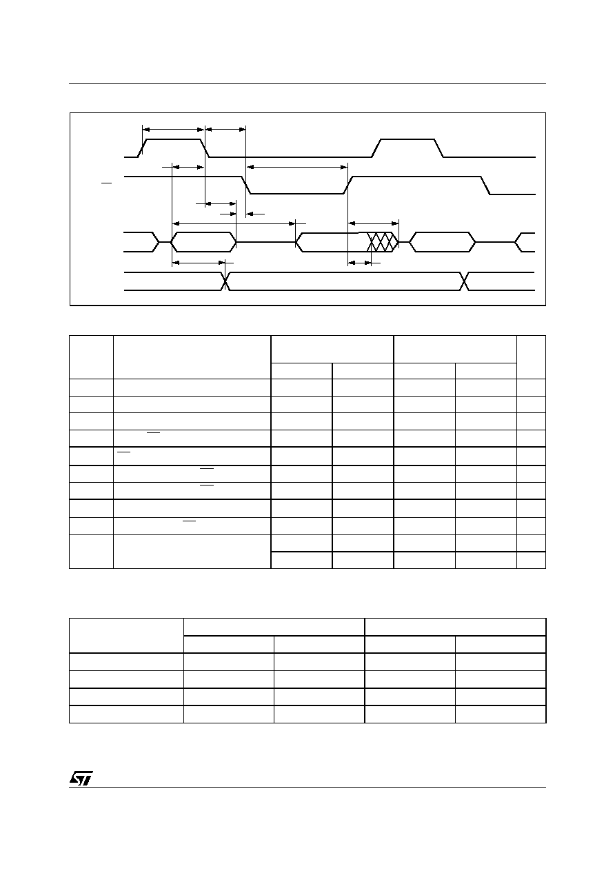
241/264
uPSD34xx - DC AND AC PARAMETERS
Figure 99. External READ Cycle (80-pin Device Only)
Table 159. External READ Cycle AC Characteristics (3V or 5V Device)
Note: 1. BUSCON Register is configured for 4 PFQCLK.
2. Refer to Table
160
for "n" and "m" values.
Table 160. n, m, and x, y Values
Symbol
Parameter
40MHz Oscillator
(1)
Variable Oscillator
1/t
CLCL
= 3 to 40MHz
Unit
Min
Max
Min
Max
t
LHLL
ALE pulse width
17
t
CLCL
≠ 8
ns
t
AVLL
Address setup to ALE
13
t
CLCL
≠ 12
ns
t
LLAX
Address hold after ALE
7.5
0.5t
CLCL
≠ 5
ns
t
LLRL
ALE to RD
7.5
0.5t
CLCL
≠ 5
ns
t
RLRH
RD pulse width
(2)
40
nt
CLCL
≠ 10
ns
t
RXIX
Input data hold after RD
2
2
ns
t
RHIZ
Input data float after RD
10.5
0.5t
CLCL
≠ 2
ns
t
AVDX
Address to valid data in
(2)
70
mt
CLCL
≠ 5
ns
t
AZRL
Address float to RD
≠2
≠2
ns
t
AVQV
Address valid to latched address out
on Ports A and B
35.5 (3V)
1.5t
CLCL
≠ 2
ns
28 (5V)
t
CLCL
≠ 9.5
ns
# of PFQCLK in
BUSCON Reg.
READ Cycle
WRITE Cycle
n
m
x
y
4
2
3
2
1
5
3
4
3
2
6
4
5
4
3
7
5
6
5
4
tAVLL
tRLRH
tRXDZ
MCU
AD0 - AD7
LATCHED
MCU
A8 - A15
AI10471
tLHLL
ALE
RD
tLLRL
A0-A7
tLLAX
tAZRL
tAVDV
A0-A7
tRXDX
tAVQV
A8-A15
DATA
IN
A8-A15
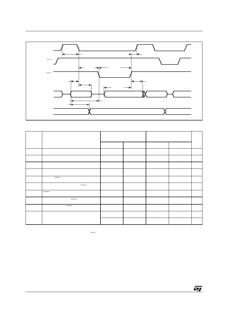
uPSD34xx - DC AND AC PARAMETERS
242/264
Figure 100. External WRITE Cycle (80-pin Device Only)
Table 161. External WRITE Cycle AC Characteristics (3V or 5V Device)
Note: 1. BUSCON Register is configured for 4 PFQCLK.
2. Refer to
Table 162., page 243
, for "n" and "m" values.
3. Latched address out on Ports A and B to WR is 2ns, minimum.
Symbol
Parameter
40MHz Oscillator
(1)
Variable Oscillator
1/t
CLCL
= 8 to 40MHz
Unit
Min
Max
Min
Max
t
LHLL
ALE pulse width
17
t
CLCL
≠ 8
ns
t
AVLL
Address Setup to ALE
13
t
CLCL
≠ 12
ns
t
LLAX
Address hold after ALE
7.5
0.5t
CLCL
≠ 5
ns
t
WLWH
WR pulse width
(2)
40
xt
CLCL
≠ 10
ns
t
LLWL
ALE to WR
7.5
0.5t
CLCL
≠ 5
ns
t
AVWL
Address (A0-A7) valid to WR
(3)
32.5
1.5t
CLCL
≠ 5
ns
t
WHLH
WR High to ALE High
9.5
9.5
0.5t
CLCL
≠ 3
0.5t
CLCL
+ 2
ns
t
QVWH
Data setup before WR
(y)
20
yt
CLCL
≠ 5
ns
t
WHQX
Data hold after WR
9.5
14.5
0.5t
CLCL
≠ 3
0.5t
CLCL
+ 2
ns
t
AVQV
Address valid to Latched Address out
on Ports A and B
35.5 (3V)
1.5t
CLCL
≠ 2
ns
28 (5V)
t
CLCL
≠ 9.5
ns
LATCHED
MCU
A8 - A15
MCU
AD0 - AD7
ALE
WR
RD
A8-A15
A8-A15
tLLWL
tWLWH
tAVLL
tLHLL
tQVWH
DATA OUT
A0-A7
DATA IN
A0-A7
tLLAX
tAVWL
tAVQV
tWHQX
tWHLH
AI10472
243/264
uPSD34xx - DC AND AC PARAMETERS
Table 162. External Clock Drive
Table 163. A/D Analog Specification
Note: 1. f
IN
2kHz, ACLK = 8MHz, AV
REF
= V
CC
= 3.3V
2. AV
REF
= V
CC
in 52-pin package.
Symbol
Parameter
(1)
40MHz Oscillator
Variable Oscillator
1/t
CLCL
= 3 to 40MHz
Unit
Min
Max
Min
Max
t
CLCL
Oscillator period
25
333
ns
t
CHCX
High time
10
t
CLCL
≠ t
CLCX
ns
t
CLCX
Low time
10
t
CLCL
≠ t
CLCX
ns
t
CLCH
Rise time
10
ns
t
CHCL
Fall time
10
ns
Symbol
Parameter
Test Conditions
(1)
Min.
Typ.
Max.
Unit
I
DD
Normal
Input = AV
REF
4.0
mA
Power-down
40
uA
AV
IN
Analog Input Voltage
GND
AV
REF
V
AV
REF
(2)
Analog Reference Voltage
3.6
V
Accuracy
Resolution
10
bits
INL
Integral Nonlinearity
Input = 0 to AV
REF
(V)
f
OSC
32MHz
±2
LSB
DNL
Differential Nonlinearity
Input = 0 to AV
REF
(V)
f
OSC
32MHz
±2
LSB
SNR
Signal to Noise Ratio
f
SAMPLE
= 500ksps
50
54
dB
SNDR
Signal to Noise Distortion Ratio
48
52
dB
ACLK
ADC Clock
2
8
16
MHz
t
C
Conversion Time
8MHz
1
4
8
µs
t
CAL
Power-up Time
Calibration Time
16
ms
f
IN
Analog Input Frequency
60
kHz
THD
Total Harmonic Distortion
50
54
dB

uPSD34xx - DC AND AC PARAMETERS
244/264
Table 164. USB Transceiver Specification
Note: 1. Temperature range = ≠45∞C to 85∞C.
2. This value includes an external resistor of 24
±1%.
Symbol
Parameter
Test Conditions
(1)
Min.
Typ.
Max.
Unit
UV
OH
High Output Voltage
V
DD
= 3.3V; I
OUT
= 2.2mA
3
≠
V
UV
OL
Low Output Voltage
V
DD
= 3.3V; I
OUT
= 2.2mA
≠
0.25
V
UV
IH
High Input Voltage
V
DD
= 3.6V
2
≠
V
UV
IL
Low Input Voltage
V
DD
= 3.6V
0.8
V
R
DH
Output Impedance (high state)
Note 2
28
43
R
DL
Output Impedance (low state)
Note 2
28
43
I
L
Input Leakage Current
V
DD
= 3.6V
±0.1
±5
µA
I
OZ
3-state Output OFF
State Current
VI = V
IH
or V
IL
±10
µA
V
CR
Crossover Point
1.3
2
V
t
RISE
Rise Time
4
20
ns
t
FALL
Fall Time
4
20
ns

245/264
uPSD34xx - DC AND AC PARAMETERS
Figure 101. Input to Output Disable / Enable
Table 165. CPLD Combinatorial Timing (5V PSD Module)
Note: 1. Fast Slew Rate output available on PA3-PA0, PB3-PB0, and PD2-PD1. Decrement times by given amount
2. t
PD
for MCU address and control signals refers to delay from pins on Port 0, Port 2, RD WR, PSEN and ALE to CPLD combinatorial
output (80-pin package only)
Table 166. CPLD Combinatorial Timing (3V PSD Module)
Note: 1. Fast Slew Rate output available on PA3-PA0, PB3-PB0, and PD2-PD1. Decrement times by given amount
2. t
PD
for MCU address and control signals refers to delay from pins on Port 0, Port 2, RD WR, PSEN and ALE to CPLD combinatorial
output (80-pin package only)
Symbol
Parameter
Conditions
Min
Max
PT
Aloc
Turbo
Off
Slew
rate
(1)
Unit
t
PD
(2)
CPLD Input Pin/Feedback to
CPLD Combinatorial Output
20
+ 2
+ 10
≠ 2
ns
t
EA
CPLD Input to CPLD Output
Enable
21
+ 10
≠ 2
ns
t
ER
CPLD Input to CPLD Output
Disable
21
+ 10
≠ 2
ns
t
ARP
CPLD Register Clear or Preset
Delay
21
+ 10
≠ 2
ns
t
ARPW
CPLD Register Clear or Preset
Pulse Width
10
+ 10
ns
t
ARD
CPLD Array Delay
Any
macrocell
11
+ 2
ns
Symbol
Parameter
Conditions
Min
Max
PT
Aloc
Turbo
Off
Slew
rate
(1)
Unit
t
PD
(2)
CPLD Input Pin/Feedback to
CPLD Combinatorial Output
35
+ 4
+ 15
≠ 6
ns
t
EA
CPLD Input to CPLD Output
Enable
38
+ 15
≠ 6
ns
t
ER
CPLD Input to CPLD Output
Disable
38
+ 15
≠ 6
ns
t
ARP
CPLD Register Clear or
Preset Delay
35
+ 15
≠ 6
ns
t
ARPW
CPLD Register Clear or
Preset Pulse Width
18
+ 15
ns
t
ARD
CPLD Array Delay
Any
macrocell
20
+ 4
ns
tER
tEA
INPUT
INPUT TO
OUTPUT
ENABLE/DISABLE
AI02863
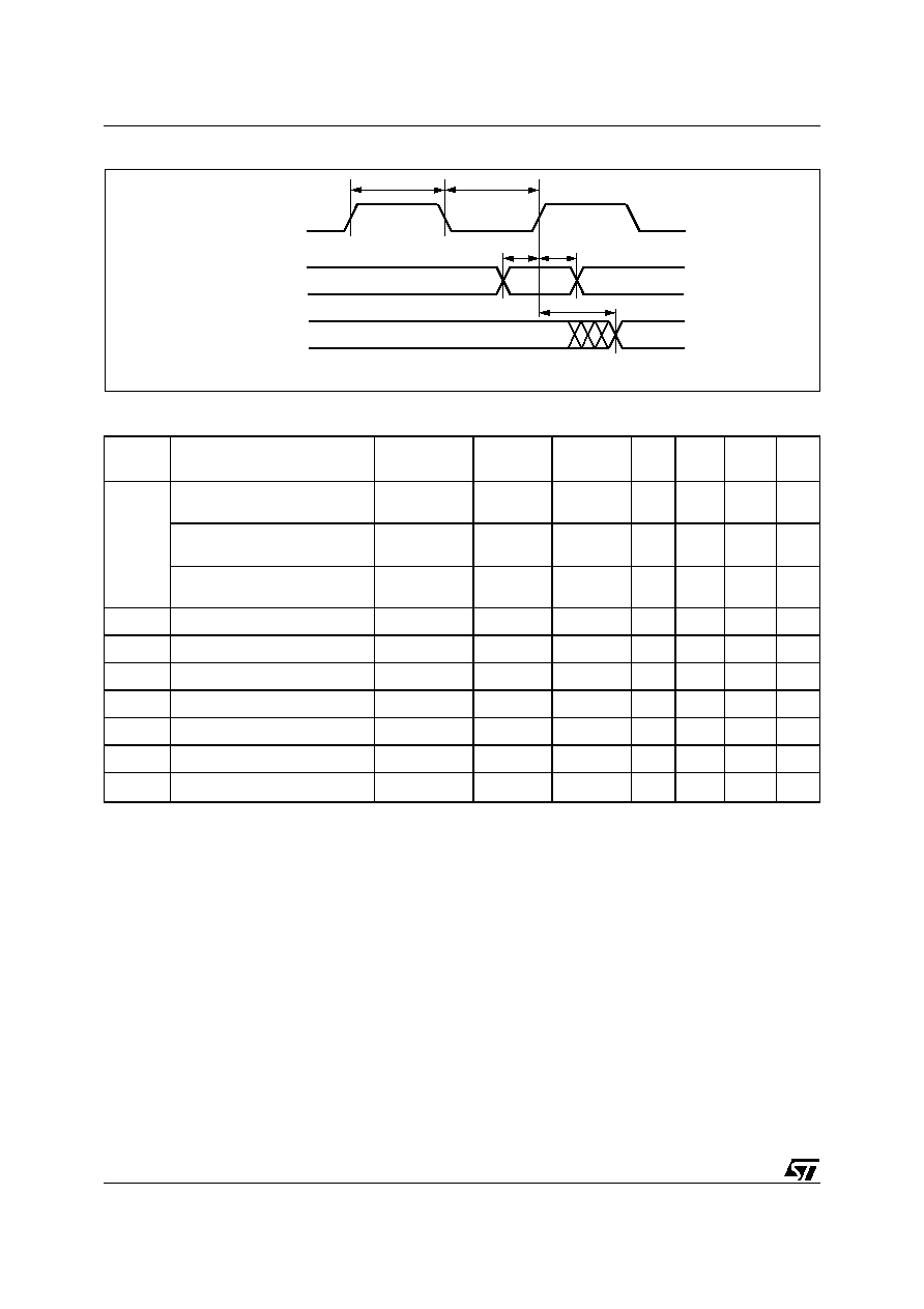
uPSD34xx - DC AND AC PARAMETERS
246/264
Figure 102. Synchronous Clock Mode Timing ≠ PLD
Table 167. CPLD Macrocell Synchronous Clock Mode Timing (5V PSD Module)
Note: 1. Fast Slew Rate output available on PA3-PA0, PB3-PB0, and PD2-PD1. Decrement times by given amount.
2. CLKIN (PD1) t
CLCL
= t
CH
+ t
CL
.105
Symbol
Parameter
Conditions
Min
Max
PT
Aloc
Turbo
Off
Slew
rate
(1)
Unit
f
MAX
Maximum Frequency
External Feedback
1/(t
S
+t
CO
)
40.0
MHz
Maximum Frequency
Internal Feedback (f
CNT
)
1/(t
S
+t
CO
≠10)
66.6
MHz
Maximum Frequency
Pipelined Data
1/(t
CH
+t
CL
)
83.3
MHz
t
S
Input Setup Time
12
+ 2
+ 10
ns
t
H
Input Hold Time
0
ns
t
CH
Clock High Time
Clock Input
6
ns
t
CL
Clock Low Time
Clock Input
6
ns
t
CO
Clock to Output Delay
Clock Input
13
≠ 2
ns
t
ARD
CPLD Array Delay
Any macrocell
11
+ 2
ns
t
MIN
Minimum Clock Period
(2)
t
CH
+t
CL
12
ns
tCH
tCL
tCO
tH
tS
CLKIN
INPUT
REGISTERED
OUTPUT
AI02860

247/264
uPSD34xx - DC AND AC PARAMETERS
Table 168. CPLD Macrocell Synchronous Clock Mode Timing (3V PSD Module)
Note: 1. Fast Slew Rate output available on PA3-PA0, PB3-PB0, and PD2-PD1. Decrement times by given amount.
2. CLKIN (PD1) t
CLCL
= t
CH
+ t
CL
.
Symbol
Parameter
Conditions
Min
Max
PT
Aloc
Turbo
Off
Slew
rate
(1)
Unit
f
MAX
Maximum Frequency
External Feedback
1/(t
S
+t
CO
)
23.2
MHz
Maximum Frequency
Internal Feedback (f
CNT
)
1/(t
S
+t
CO
≠10)
30.3
MHz
Maximum Frequency
Pipelined Data
1/(t
CH
+t
CL
)
40.0
MHz
t
S
Input Setup Time
20
+ 4
+ 15
ns
t
H
Input Hold Time
0
ns
t
CH
Clock High Time
Clock Input
15
ns
t
CL
Clock Low Time
Clock Input
10
ns
t
CO
Clock to Output Delay
Clock Input
23
≠ 6
ns
t
ARD
CPLD Array Delay
Any macrocell
20
+ 4
ns
t
MIN
Minimum Clock Period
(2)
t
CH
+t
CL
25
ns
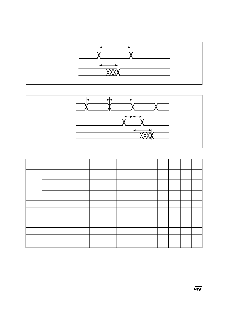
uPSD34xx - DC AND AC PARAMETERS
248/264
Figure 103. Asynchronous RESET / Preset
Figure 104. Asynchronous Clock Mode Timing (Product Term Clock)
Table 169. CPLD Macrocell Asynchronous Clock Mode Timing (5V PSD Module)
Symbol
Parameter
Conditions
Min
Max
PT
Aloc
Turbo
Off
Slew
Rate
Unit
f
MAXA
Maximum Frequency
External Feedback
1/(t
SA
+t
COA
)
38.4
MHz
Maximum Frequency
Internal Feedback (f
CNTA
)
1/(t
SA
+t
COA
≠10)
62.5
MHz
Maximum Frequency
Pipelined Data
1/(t
CHA
+t
CLA
)
71.4
MHz
t
SA
Input Setup Time
7
+ 2
+ 10
ns
t
HA
Input Hold Time
8
ns
t
CHA
Clock Input High Time
9
+ 10
ns
t
CLA
Clock Input Low Time
9
+ 10
ns
t
COA
Clock to Output Delay
21
+ 10
≠ 2
ns
t
ARDA
CPLD Array Delay
Any macrocell
11
+ 2
ns
t
MINA
Minimum Clock Period
1/f
CNTA
16
ns
tARP
REGISTER
OUTPUT
tARPW
RESET/PRESET
INPUT
AI02864
tCHA
tCLA
tCOA
tHA
tSA
CLOCK
INPUT
REGISTERED
OUTPUT
AI02859

249/264
uPSD34xx - DC AND AC PARAMETERS
Table 170. CPLD Macrocell Asynchronous Clock Mode Timing (3V PSD Module)
Symbol
Parameter
Conditions
Min
Max
PT
Aloc
Turbo
Off
Slew
Rate
Unit
f
MAXA
Maximum Frequency
External Feedback
1/(t
SA
+t
COA
)
21.7
MHz
Maximum Frequency
Internal Feedback (f
CNTA
)
1/(t
SA
+t
COA
≠10)
27.8
MHz
Maximum Frequency
Pipelined Data
1/(t
CHA
+t
CLA
)
33.3
MHz
t
SA
Input Setup Time
10
+ 4
+ 15
ns
t
HA
Input Hold Time
12
ns
t
CHA
Clock High Time
17
+ 15
ns
t
CLA
Clock Low Time
13
+ 15
ns
t
COA
Clock to Output Delay
31
+ 15
≠ 6
ns
t
ARD
CPLD Array Delay
Any macrocell
20
+ 4
ns
t
MINA
Minimum Clock Period
1/f
CNTA
36
ns
uPSD34xx - DC AND AC PARAMETERS
250/264
Figure 105. Input Macrocell Timing (Product Term Clock)
Table 171. Input Macrocell Timing (5V PSD Module)
Note: 1. Inputs from Port A, B, and C relative to register/ latch clock from the PLD. ALE/AS latch timings refer to t
AVLX
and t
LXAX
.
Table 172. Input Macrocell Timing (3V PSD Module)
Note: 1. Inputs from Port A, B, and C relative to register/latch clock from the PLD. ALE latch timings refer to t
AVLX
and t
LXAX
.
Symbol
Parameter
Conditions
Min
Max
PT
Aloc
Turbo
Off
Unit
t
IS
Input Setup Time
(Note
1)
0
ns
t
IH
Input Hold Time
(Note
1)
15
+ 10
ns
t
INH
NIB Input High Time
(Note
1)
9
ns
t
INL
NIB Input Low Time
(Note
1)
9
ns
t
INO
NIB Input to Combinatorial Delay
(Note
1)
34
+ 2
+ 10
ns
Symbol
Parameter
Conditions
Min
Max
PT
Aloc
Turbo
Off
Unit
t
IS
Input Setup Time
(Note
1)
0
ns
t
IH
Input Hold Time
(Note
1)
25
+ 15
ns
t
INH
NIB Input High Time
(Note
1)
12
ns
t
INL
NIB Input Low Time
(Note
1)
12
ns
t
INO
NIB Input to Combinatorial Delay
(Note
1)
43
+ 4
+ 15
ns
t
INH
t
INL
t
INO
t
IH
t
IS
PT CLOCK
INPUT
OUTPUT
AI03101
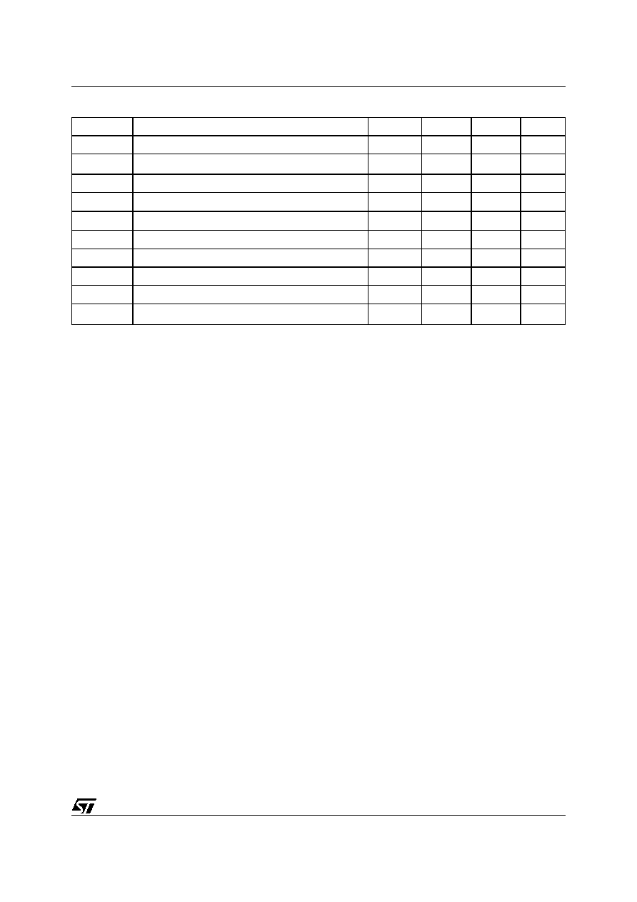
251/264
uPSD34xx - DC AND AC PARAMETERS
Table 173. Program, WRITE and Erase Times (5V, 3V PSD Modules)
Note: 1. Programmed to all zero before erase.
2. Typical after 100K Write/Erase cycles is 5 seconds.
3. The polling status, DQ7, is valid t
Q7VQV
time units before the data byte, DQ0-DQ7, is valid for reading.
Symbol
Parameter
Min.
Typ.
Max.
Unit
Flash Program
8.5
s
Flash Bulk Erase
(1)
(pre-programmed)
3
(2)
10
s
Flash Bulk Erase (not pre-programmed)
5
s
t
WHQV3
Sector Erase (pre-programmed)
1
10
s
t
WHQV2
Sector Erase (not pre-programmed)
2.2
s
t
WHQV1
Byte Program
14
150
µs
Program / Erase Cycles (per Sector)
100,000
cycles
PLD Program / Erase Cycles
1,000
cycles
t
WHWLO
Sector Erase Time-Out
100
µs
t
Q7VQV
DQ7 Valid to Output (DQ7-DQ0) Valid (Data Polling)
(3)
30
ns
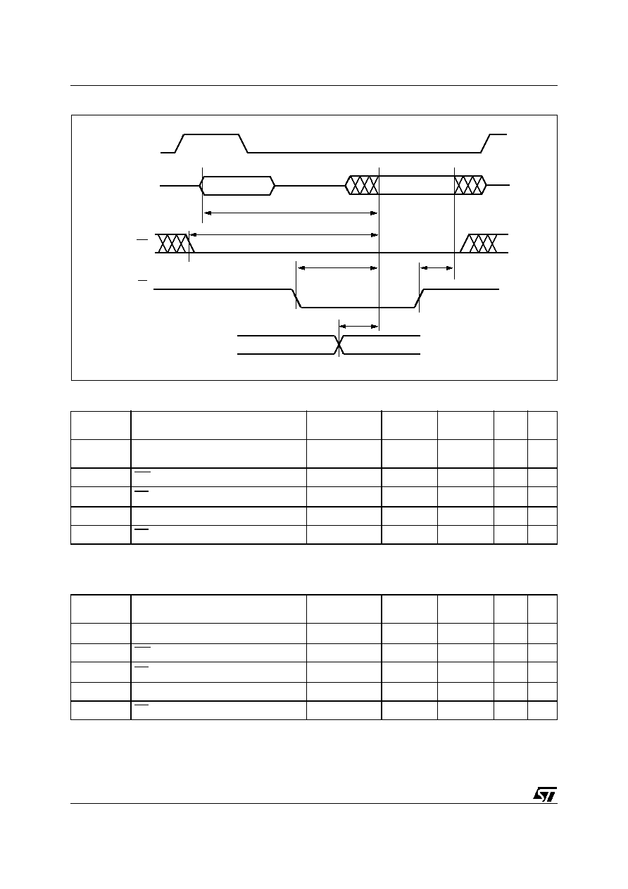
uPSD34xx - DC AND AC PARAMETERS
252/264
Figure 106. Peripheral I/O READ Timing
Table 174. Port A Peripheral Data Mode READ Timing (5V PSD Module)
Note: 1. Any input used to select Port A Data Peripheral Mode.
2. Data is already stable on Port A.
Table 175. Port A Peripheral Data Mode READ Timing (3V PSD Module)
Note: 1. Any input used to select Port A Data Peripheral Mode.
2. Data is already stable on Port A.
Symbol
Parameter
Conditions
Min
Max
Turbo
Off
Unit
t
AVQV≠PA
Address Valid to Data
Valid
(Note
1)
37
+ 10
ns
t
SLQV≠PA
CSI Valid to Data Valid
27
+ 10
ns
t
RLQV≠PA
RD to Data Valid
(Note
2)
32
ns
t
DVQV≠PA
Data In to Data Out Valid
22
ns
t
RHQZ≠PA
RD to Data High-Z
23
ns
Symbol
Parameter
Conditions
Min
Max
Turbo
Off
Unit
t
AVQV≠PA
Address Valid to Data Valid
(Note
1)
50
+ 15
ns
t
SLQV≠PA
CSI Valid to Data Valid
37
+ 15
ns
t
RLQV≠PA
RD to Data Valid
(Note
2)
45
ns
t
DVQV≠PA
Data In to Data Out Valid
38
ns
t
RHQZ≠PA
RD to Data High-Z
36
ns
tRLQV (PA)
tDVQV (PA)
tRHQZ (PA)
tSLQV (PA)
tAVQV (PA)
ADDRESS
DATA VALID
ALE
A /D BUS
RD
DATA ON PORT A
CSI
AI06610
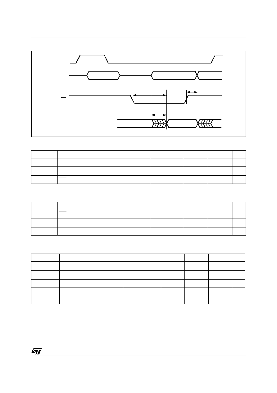
253/264
uPSD34xx - DC AND AC PARAMETERS
Figure 107. Peripheral I/O WRITE Timing
Table 176. Port A Peripheral Data Mode WRITE Timing (5V PSD Module)
Note: 1. Data stable on Port 0 pins to data on Port A.
Table 177. Port A Peripheral Data Mode WRITE Timing (3V PSD Module)
Note: 1. Data stable on Port 0 pins to data on Port A.
Table 178. Supervisor Reset and LVD
Note: 1. 25µs minimum to abort a Flash memory program or erase cycle in progress.
2. As f
OSC
decreases, t
RST_ACTV
increases. Example: t
RST_ACTV
= 50ms when f
OSC
= 8MHz.
Symbol
Parameter
Conditions
Min
Max
Unit
t
WLQV≠PA
WR to Data Propagation Delay
25
ns
t
DVQV≠PA
Data to Port A Data Propagation Delay
(Note
1)
22
ns
t
WHQZ≠PA
WR Invalid to Port A Tri-state
20
ns
Symbol
Parameter
Conditions
Min
Max
Unit
t
WLQV≠PA
WR to Data Propagation Delay
42
ns
t
DVQV≠PA
Data to Port A Data Propagation Delay
(Note
1)
38
ns
t
WHQZ≠PA
WR Invalid to Port A Tri-state
33
ns
Symbol
Parameter
Conditions
Min
Typ
Max
Unit
t
RST_LO_IN
Reset Input Duration
1
(1)
µs
t
RST_ACTV
Generated Reset Duration
f
OSC
= 40MHz
10
(2)
ms
t
RST_FIL
Reset Input Spike Filter
1
µs
V
RST_HYS
Reset Input Hysteresis
V
CC
= 3.3V
0.1
V
V
RST_THRESH
LVD Trip Threshold
V
CC
= 3.3V
2.4
2.6
2.8
V
tDVQV (PA)
tWLQV (PA)
tWHQZ (PA)
ADDRESS
DATA OUT
A / D BUS
WR
PORT A
DATA OUT
ALE
AI06611

uPSD34xx - DC AND AC PARAMETERS
254/264
Table 179. V
STBYON
Definitions Timing (5V, 3V PSD Modules)
Note: 1. V
STBYON
timing is measured at V
CC
ramp rate of 2ms.
Figure 108. ISC Timing
Table 180. ISC Timing (5V PSD Module)
Note: 1. For non-PLD Programming, Erase or in ISC By-pass Mode.
2. For Program or Erase PLD only.
Symbol
Parameter
Conditions
Min
Typ
Max
Unit
t
BVBH
V
STBY
Detection to V
STBYON
Output High
(Note
1)
20
µs
t
BXBL
V
STBY
Off Detection to V
STBYON
Output
Low
(Note
1)
20
µs
Symbol
Parameter
Conditions
Min
Max
Unit
t
ISCCF
Clock (TCK, PC1) Frequency (except for PLD)
(Note
1)
20
MHz
t
ISCCH
Clock (TCK, PC1) High Time (except for PLD)
(Note
1)
23
ns
t
ISCCL
Clock (TCK, PC1) Low Time (except for PLD)
(Note
1)
23
ns
t
ISCCFP
Clock (TCK, PC1) Frequency (PLD only)
(Note
2)
4
MHz
t
ISCCHP
Clock (TCK, PC1) High Time (PLD only)
(Note
2)
90
ns
t
ISCCLP
Clock (TCK, PC1) Low Time (PLD only)
(Note
2)
90
ns
t
ISCPSU
ISC Port Set Up Time
7
ns
t
ISCPH
ISC Port Hold Up Time
5
ns
t
ISCPCO
ISC Port Clock to Output
21
ns
t
ISCPZV
ISC Port High-Impedance to Valid Output
21
ns
t
ISCPVZ
ISC Port Valid Output to High-Impedance
21
ns
ISCCH
TCK
TDI/TMS
ISC OUTPUTS/TDO
ISC OUTPUTS/TDO
t
ISCCL
t
ISCPH
t
ISCPSU
t
ISCPVZ
t
ISCPZV
t
ISCPCO
t
AI02865

255/264
uPSD34xx - DC AND AC PARAMETERS
Table 181. ISC Timing (3V PSD Module)
Note: 1. For non-PLD Programming, Erase or in ISC By-pass Mode.
2. For Program or Erase PLD only.
Figure 109. MCU Module AC Measurement I/O Waveform
Note: AC inputs during testing are driven at V
CC
≠0.5V for a logic '1,' and 0.45V for a logic '0.'
Timing measurements are made at V
IH
(min) for a logic '1,' and V
IL
(max) for a logic '0'
Figure 110. PSD Module AC Float I/O Waveform
Note: For timing purposes, a Port pin is considered to be no longer floating when a 100mV change from load voltage occurs, and begins to
float when a 100mV change from the loaded V
OH
or V
OL
level occurs
I
OL
and I
OH
20mA
Symbol
Parameter
Conditions
Min
Max
Unit
t
ISCCF
Clock (TCK, PC1) Frequency (except for PLD)
(Note
1)
16
MHz
t
ISCCH
Clock (TCK, PC1) High Time (except for PLD)
(Note
1)
40
ns
t
ISCCL
Clock (TCK, PC1) Low Time (except for PLD)
(Note
1)
40
ns
t
ISCCFP
Clock (TCK, PC1) Frequency (PLD only)
(Note
2)
4
MHz
t
ISCCHP
Clock (TCK, PC1) High Time (PLD only)
(Note
2)
90
ns
t
ISCCLP
Clock (TCK, PC1) Low Time (PLD only)
(Note
2)
90
ns
t
ISCPSU
ISC Port Set Up Time
12
ns
t
ISCPH
ISC Port Hold Up Time
5
ns
t
ISCPCO
ISC Port Clock to Output
30
ns
t
ISCPZV
ISC Port High-Impedance to Valid Output
30
ns
t
ISCPVZ
ISC Port Valid Output to High-Impedance
30
ns
AI06650
VCC ≠ 0.5V
0.45V
Test Points
0.2 VCC ≠ 0.1V
0.2 VCC + 0.9V
AI06651
Test Reference Points
VOL + 0.1V
VOH ≠ 0.1V
VLOAD ≠ 0.1V
VLOAD + 0.1V
0.2 VCC ≠ 0.1V

uPSD34xx - DC AND AC PARAMETERS
256/264
Figure 111. External Clock Cycle
Figure 112. PSD Module AC Measurement I/O
Waveform
Figure 113. PSD Module AC Measurement
Load Circuit
Table 182. I/O Pin Capacitance
Note: 1. Sampled only, not 100% tested.
2. Typical values are for T
A
= 25∞C and nominal supply voltages.
3. Maximum for MCU Address and Data lines is 20pF each.
3.0V
0V
Test Point
1.5V
AI03103b
Device
Under Test
2.01 V
195
C
L
= 30 pF
(Including Scope and
Jig Capacitance)
AI03104b
Symbol
Parameter
(1)
Test Condition
Typ.
(2)
Max.
Unit
C
IN
Input Capacitance (for input pins)
V
IN
= 0V
4
6
pF
C
OUT
Output Capacitance (for input/
output pins)
(3)
V
OUT
= 0V
8
12
pF
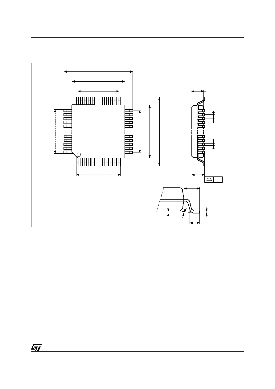
257/264
uPSD34xx - PACKAGE MECHANICAL INFORMATION
PACKAGE MECHANICAL INFORMATION
Figure 114. TQFP52 ≠ 52-lead Plastic Thin, Quad, Flat Package Outline
Note: Drawing is not to scale.
QFP-A
Nd
E1
CP
b
e
A2
A
N
L
A1
D1
D
1
E
Ne
c
D2
E2
L1

uPSD34xx - PACKAGE MECHANICAL INFORMATION
258/264
Table 183. TQFP52 ≠ 52-lead Plastic Thin, Quad, Flat Package Mechanical Data
Symb
mm
inches
Typ
Min
Max
Typ
Min
Max
A
1.50
≠
1.70
0.059
≠
0.067
A1
0.10
0.05
0.20
0.004
0.002
0.008
A2
1.40
1.30
1.50
0.055
0.039
0.059
b
≠
0.20
0.40
≠
0.008
0.016
c
≠
0.07
0.20
≠
0.003
0.008
D
12.00
11.80
12.20
0.472
0.465
0.480
D1
10.00
9.80
10.20
0.394
0.386
0.402
D2
7.80
7.67
7.93
0.307
0.302
0.312
E
12.00
11.80
12.20
0.472
0.465
0.480
E1
10.00
9.80
10.20
0.394
0.386
0.402
E2
7.80
7.67
7.93
0.307
0.302
0.312
e
0.65
≠
≠
0.026
≠
≠
L
≠
0.45
0.75
≠
0.018
0.030
L1
1.00
≠
≠
0.039
≠
≠
≠
0∞
7∞
≠
0∞
7∞
n
52
52
Nd
13
13
Ne
13
13
CP
≠
≠
0.10
≠
≠
0.004
259/264
uPSD34xx - PACKAGE MECHANICAL INFORMATION
Figure 115. TQFP80 ≠ 80-lead Plastic Thin, Quad, Flat Package Outline
Note: Drawing is not to scale.
QFP-A
Nd
E1
CP
b
e
A2
A
N
L
A1
D1
D
1
E
Ne
c
D2
E2
L1
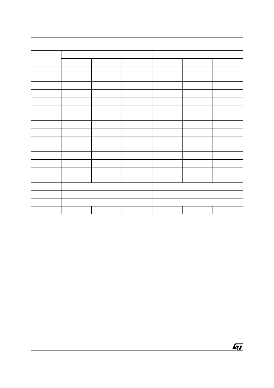
uPSD34xx - PACKAGE MECHANICAL INFORMATION
260/264
Table 184. TQFP80 ≠ 80-lead Plastic Thin, Quad, Flat Package Mechanical Data
Symb
mm
inches
Typ
Min
Max
Typ
Min
Max
A
1.60
0.063
A1
0.05
0.15
0.002
0.006
A2
1.40
1.35
1.45
0.055
0.053
0.057
b
0.17
0.27
0.007
0.011
c
0.09
0.20
0.004
0.008
D
14.00
0.551
D1
12.00
0.472
D2
9.50
0.374
E
14.00
0.551
E1
12.00
0.472
E2
9.50
0.374
e
0.50
0.020
L
0.45
0.75
0.018
0.030
L1
1.00
0.039
0∞
7∞
0∞
7∞
n
80
80
Nd
20
20
Ne
20
20
CP
0.08
0.003

261/264
uPSD34xx - PART NUMBERING
PART NUMBERING
Table 185. Ordering Information Scheme
For other options, or for more information on any aspect of this device, please contact the ST Sales Office
nearest you.
Example:
UPSD
34
3
4
E
V
≠
40
U
6
T
Device Type
uPSD = Microcontroller PSD
Family
34 = Turbo Plus core
SRAM Size
2 = 4Kbyte
3 = 8Kbyte
Main Flash Memory Size
2 = 64Kbyte
3 = 128Kbyte
4 = 256Kbyte
IP Mix
E = IP Mix: USB, I
2
C, SPI, UART (2), IrDA, ADC, Supervisor, PCA
Operating Voltage
blank = V
CC
= 4.5 to 5.5V
V = V
CC
= 3.0 to 3.6V
Speed
≠40 = 40MHz
Package
T = 52-pin TQFP
U = 80-pin TQFP
Temperature Range
6 = ≠40 to 85∞C
Shipping Option
Tape & Reel Packing = T

uPSD34xx - IMPORTANT NOTES
262/264
IMPORTANT NOTES
The following sections describe the limitations that
apply to the uPSD34xx devices.
USB Interrupts with Idle Mode
Description
An interrupt generated by a USB related event
does not bring the MCU out of idle mode for pro-
cessing.
Impact On Application
Idle mode cannot be used with USB.
Workaround
None identified at this time.
USB Reset Interrupt
Description
When the MCU clock prescaler is set to a value
other than f
MCU
= f
OSC
(no division), a reset signal
on the USB does not cause a USB interrupt to be
generated.
Impact On Application
An MCU clock other than that equal to the frequen-
cy of the oscillator cannot be used.
Workaround
The CPUPS field in the CCON0 register must be
set to 000b (default after reset). The 3400 USB
firmware examples set CCON0 register to 000b.
USB Reset
Description
A USB reset does not reset the USB SIE's regis-
ters.
Impact On Application
A USB reset does not reset the USB SIE's regis-
ters as does a power-on or hardware reset.
Workaround
When a USB reset is detected, the USB SIE's reg-
isters must be initialized appropriately by the fir-
ware. The 3400 USB firmware examples clear
USB SIE's if USB reset is detected.
Data Toggle
Description
The data toggle bit is read only.
Impact On Application
The IN FIFO data toggle bit is controlled exclusive-
ly by the USB SIE; therefore, it is not possible to
change the state of the data toggle bit by firmware.
Workaround
For cases where the data toggle bit must be reset,
such as after a Clear Feature/Stall request, send-
ing the subsequent data on that endpoint twice re-
sults in getting the data toggle bit back to the state
that it should be.
USB FIFO Accessibility
Description
The USB FIFO is only accessible by firmware and
not by a JTAG debugger.
Impact On Application
Using a JTAG debugger, it is not possible to view
the USB FIFO's contents in a memory dump win-
dow.
Workaround
None identified at this time.
Erroneous Resend of Data Packet
Description
When a data packet is sent the respective IN FIFO
busy bit is not automatically cleared by the USB
SIE. This can cause a data packet to be errone-
ously resent to the host in response to an IN PID
immediately after the first correct transmission of
this data packet.
Impact On Application
Since the Data Toggle in the retransmitted data
packet is toggled from when the data was first
sent, the host will treat this packet as valid. If the
identified workaround is not implemented then this
extra and unexpected data packet would result in
a communication breakdown.

263/264
uPSD34xx - IMPORTANT NOTES
Workaround
In the USB ISR, when an INx (x = the endpoint
number of the IN FIFO) is detected, the IN FIFOs
respective busy bit should be unconditionally
cleared. The 3400 USB firmware implements this
workaround.
IN FIFO Pairing Operation
Description
FIFO pairing is not available on IN endpoints. Sin-
gle FIFO buffering should be used instead.
Impact On Application
Use Single FIFO Buffering.
Workaround
Only use the single-FIFO mode. The 3400 USB
firmware implements this workaround.
PORT 1 Not 5-volt IO Tolerant
Description
The port P1 is shared with the ADC module and as
a result Port P1 is not 5V tolerant.
Impact On Application
5V devices should not be connected to port P1.
Workaround
Peripherals or GPIO that require 5-Volt IO toler-
ance should be mapped to Port 3 or Port 4.

uPSD34xx - REVISION HISTORY
264/264
REVISION HISTORY
Table 186. Document Revision History
Date
Version
Revision Details
04-Feb-2005
1.0
First Edition
30-Mar-2005
2.0
Added one note in
SUMMARY DESCRIPTION, page 7
Added two notes in
USB INTERFACE, page 123
Changed values in
Table 175., page 252
(Turbo Off column)
Added
IMPORTANT NOTES, page 262
Information furnished is believed to be accurate and reliable. However, STMicroelectronics assumes no responsibility for the consequences
of use of such information nor for any infringement of patents or other rights of third parties which may result from its use. No license is granted
by implication or otherwise under any patent or patent rights of STMicroelectronics. Specifications mentioned in this publication are subject
to change without notice. This publication supersedes and replaces all information previously supplied. STMicroelectronics products are not
authorized for use as critical components in life support devices or systems without express written approval of STMicroelectronics.
The ST logo is a registered trademark of STMicroelectronics.
All other names are the property of their respective owners
© 2005 STMicroelectronics - All rights reserved
STMicroelectronics group of companies
Australia ≠ Belgium - Brazil - Canada - China ≠ Czech Republic - Finland - France - Germany - Hong Kong - India - Israel - Italy - Japan -
Malaysia - Malta - Morocco - Singapore - Spain - Sweden - Switzerland - United Kingdom - United States of America
www.st.com