 | –≠–ª–µ–∫—Ç—Ä–æ–Ω–Ω—ã–π –∫–æ–º–ø–æ–Ω–µ–Ω—Ç: USBDF01W5 | –°–∫–∞—á–∞—Ç—å:  PDF PDF  ZIP ZIP |
1/9
USBDFxxW5
Æ
EMI FILTER AND LINE TERMINATION
FOR USB DOWNSTREAM PORTS
May 2000 Ed : 1C
A.S.D.
TM
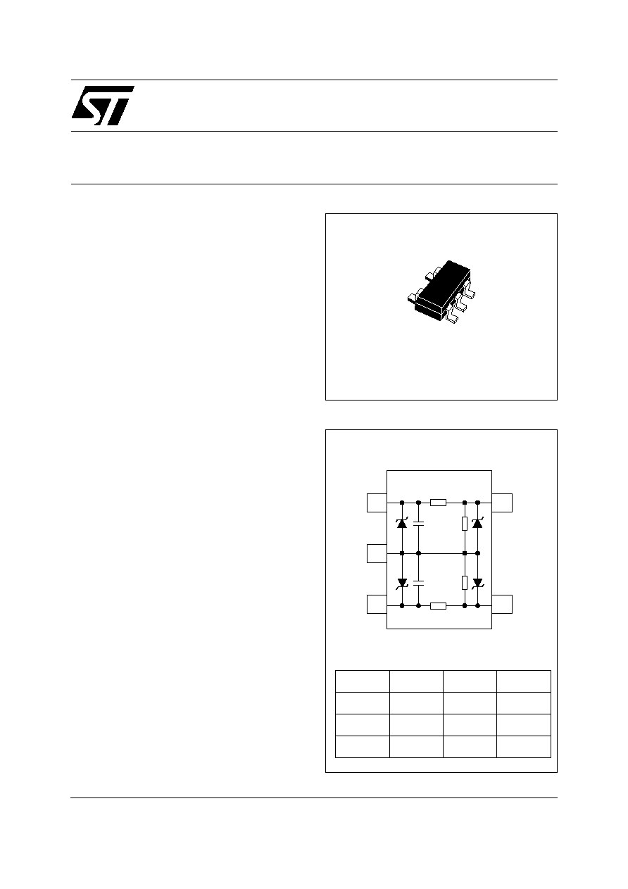
SOT323-5L
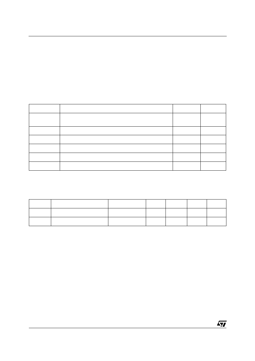
FUNCTIONAL DIAGRAM
TM: ASD and TRANSIL are a trademarks of STMicroelectronics.
EMI Filter and line termination for USB down-
stream ports on:
- Desktop computer
- Notebooks
- Workstations
- USB Hubs
APPLICATIONS
n
Monolithic device with recommended line termi-
nation for USB downstream ports
n
Integrated Rt series termination and Ct bypass-
ing capacitors.
n
Integrated ESD protection
n
Small package size
FEATURES
The
USB
specification
requires
USB
downstream
ports
to
be
terminated
with
pull-down resistors from the D+ and D- lines to
ground.
On
the
implementation
of
USB
systems, the radiated and conducted EMI
should be kept within the required levels as
stated by the FCC regulations. In addition to
the requirements of termination and EMC
compatibility,
the
computing
devices
are
required to be tested for ESD susceptibility.
The USBDFxxW5 provides the recommended line
termination while implementing a low pass filter to
limit EMI levels and providing ESD protection
which exceeds IEC 61000-4-2 level 4 standard.
The device is packaged in a SOT323-5L which is
the smallest available lead frame package (50%
smaller than the standard SOT23).
DESCRIPTION
n
EMI / RFI noise suppression
n
Required line termination for USB downstream
ports
n
ESD protection exceeding IEC61000-4-2 level 4
n
High flexibility in the design of high density
boards
n
Tailored to meet USB 1.1 standard
BENEFITS
D+ In
D- In
Gnd
D+ Out
D- Out
Rt
Rd
Ct
Rt
Ct
Rd
Rt
Rd
Ct
Code 01
33
15k
47pF
Code 02
15
15k
47pF
Tolerance
±10%
±10%
±20%
USBDFxxW5
2/9
IEC-61000-4-2, level 4
±15 kV (air discharge)
±8 kV (contact discharge)
MIL STD 883C, Method 3015-6
Class 3 C = 100 pF R = 1500
3 positive strikes and 3 negative strikes (F = 1 Hz)
COMPLIES WITH THE FOLLOWING ESD
STANDARDS:
Symbol
Parameter
Value
Unit
V
PP
ESD discharge IEC 61000-4-2, contact discharge
ESD discharge - MIL STD 883 - Method 3015-6
±15
±25
kV
kV
T
j
Junction temperature
150
∞C
T
stg
Storage temperature range
- 55 to +150
∞C
T
L
Lead solder temperature (10 second duration)
260
∞C
T
op
Operating temperature Range
0 to 70
∞C
P
r
Power rating per resistor
100
mW
ABSOLUTE MAXIMUM RATINGS (T
amb
= 25∞C)
Symbol
Parameters
Test conditions
Min
Typ
Max
Unit
V
BR
Diode breakdown voltage
I
R
= 1mA
6
V
V
F
Diode forward voltage drop
I
F
= 50mA
0.9
V
ELECTRICAL CHARACTERISTICS (T
amb
= 25∞C)
USBDFxxW5
3/9
D+
Peripheral
transceiver
D-
CABLE
Host/Hub USB
port transceiver
D- (2)
D+ (1)
D+ (2)
D- (1)
(1) for a low-speed port
(2) for a full-speed port
+Vbus
Upstream port
Downstream port
USBDF
xxW5
USBUF
xxW6
APPLICATION EXAMPLE
Host or
Hub port
Twisted pair shielded
Zo = 90ohms
5m max
Hub 0 or
Full-speed function
Untwisted unshielded
3m max
FULL SPEED CONNECTION
LOW SPEED CONNECTION
+Vbus
+Vbus
D+
D-
D+
D-
D+
D-
D+
D-
1.5k
1.5k
Hub 0 or
Low-speed function
Low-speed USB
Transceiver
Full-speed or
Low-speed USB
Transceiver
15k
Rt
Rt
Ct
Ct
Host or
Hub port
Full-speed or
Low-speed USB
Transceiver
15k
Rt
Rt
Ct
Ct
Rt
Rt
Ct
Ct
Full-speed USB
Transceiver
Rt
Rt
Ct
Ct
15k
15k
Fig. A1: USB Standard requirements
APPLICATION INFORMATION
USBDFxxW5
4/9
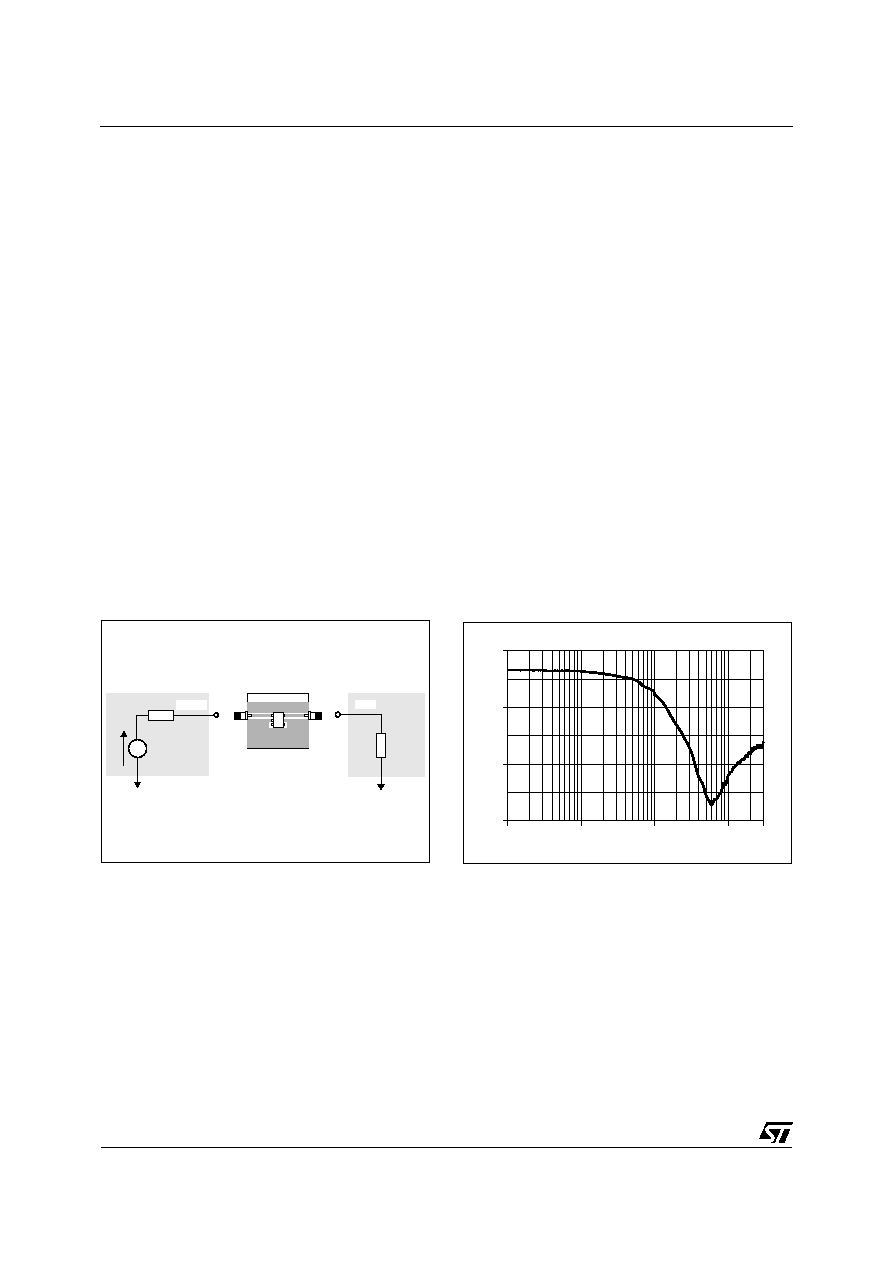
50
RF IN
Vg
50
TG OUT
TEST BOARD
UD1
Fig. A2: Measurement configuration
1
10
100
1000 3000
-30
-20
-10
0
F (MHz)
Insertion loss (dB)
Fig. A3: USBDFxxW5 attenuation curve.
In addition to the requirements of termination and EMC compatibility, computing devices are required to be
tested for ESD susceptibility. This test is described in the IEC 61000-4-2 and is already in place in Europe.
This test requires that a device tolerates ESD events and remain operational without user intervention.
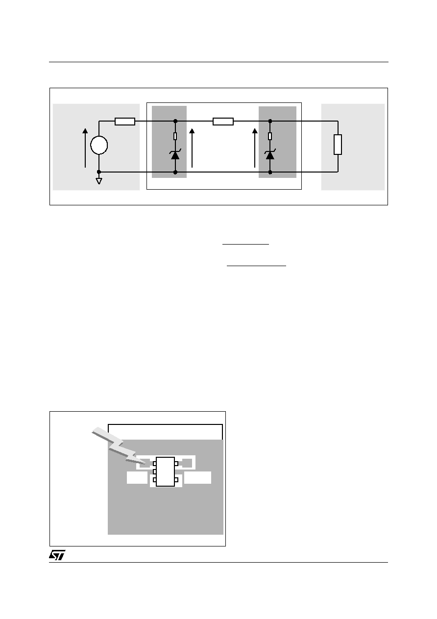
The USBDFxxW5 is particularly optimized to perform ESD protection. ESD protection is based on the use
of device which clamps at :
Vinput
V
R I
BR
d
PP
=
+
.
This protection function is splitted in 2 stages. As shown in figure A4, the ESD strikes are clamped by the
first stage S1 and then its remaining overvoltage is applied to the second stage through the resistor R.
Such a configuration makes the output voltage very low at the Vout level.
ESD PROTECTION
Current FCC regulations requires that class B computing devices meet specified maximum levels for both
ratiated and conducted EMI.
- Radiated EMI covers the frequency range from 30MHz to 1GHz.
- Conducted EMI covers the 450kHz to 30MHz range.
For the types of devices utilizing the USB the most difficult test to pass is usually the radiated EMI test. For
this reason the USBDF device is aiming to minimize radiated EMI.
The differential signal (D+ and D-) of the USB does not contribute significantly to radiated or conducted
EMI because the magnetic field of the two conductors exactly cancels each other.
The inside of the PC environment is very noisy and designers must minimise noise coupling from the differ-
ent sources. D+ and D- must not be routed near high speed lines (clocks...).
Induced common mode noise can be minimised by running pairs of USB signals parallel to each other and
running grounded guard trace on each side of the signal pair from the USB controller to the USBDF device.
If possible, locate the USBDF device physically near the USB connectors. Distance between the USB con-
troller and the USB connector must be minimized.
The 47pF (Ct) capacitors are used to bypass high frequency energy to ground and for edge control, and
must be placed between the USB Controller and the series termination resistors (Rt). Both Ct and Rt
should be placed as close to the USB Controller as practicable.
The USBDFxxW5 ensure a filtering protection against ElectroMagnetic and RadioFrequency Interferences
thanks to its low-pass filter structure. This filter is characterized by the following parameters :
- cut-off frequency
- Insertion loss
- high frequency rejection
Fig. A3 shows the attenuation curve for frequencies up to 3GHz.
EMI FILTERING
USBDFxxW5
5/9
To have a good approximation of the remaining voltages at both Vin and Vout stages, we give the typical
dynamical resistance value Rd. By taking into account these following hypothesis : Rt>Rd, Rg>Rd and
Rload>Rd, it gives these formulas:
Vinput
R V
R V
R
g
BR
d
g
g
=
+
.
.
Voutput
R V
R Vinput
R
t
BR
d
t
=
+
.
.
The results of the calculation done for V
PP
=8kV, Rg=330
(IEC61000-4-2 standard), V
BR
=7V (typ.)
and Rd = 1
(typ.) give:
Vinput = 31.2 V
Voutput = 7.95 V
This confirms the very low remaining voltage across the device to be protected. It is also important to note
that in this approximation the parasitic inductance effect was not taken into account. This could be few
tenths of volts during few ns at the Vin side. This parasitic effect is not present at the Vout side due the low
current involved after the resistance R.
The measurements done here after show very clearly (Fig. A6) the high efficiency of the ESD protection :
- no influence of the parasitic inductances on Vout stage
- output clamping voltage very close to V
BR
(positive strike) and -V
F
(negative strike)
TEST BOARD
ESD
SURGE
16kV
Air
Discharge
Vin
Vout
UD1
Fig. A5: Measurement board
ESD Surge
Vinput
Voutput
Rload
Rg
R
S1
Rd
V
BR
V
BR
V
PP
Device
to be
protected
USBDFxxW5
Rd
S2
Fig. A4: USBDFxxW5 ESD clamping behavior