 | –≠–ª–µ–∫—Ç—Ä–æ–Ω–Ω—ã–π –∫–æ–º–ø–æ–Ω–µ–Ω—Ç: VB027BSP | –°–∫–∞—á–∞—Ç—å:  PDF PDF  ZIP ZIP |
June 1999
1/7
Æ
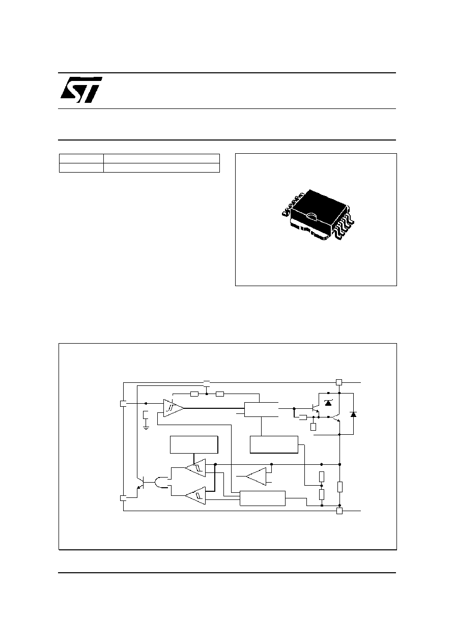
VB027BSP
HIGH VOLTAGE IGNITION COIL DRIVER
POWER I.C.
s
PRIMARY COIL VOLTAGE INTERNALLY SET
s
COIL CURRENT LIMIT INTERNALLY SET
s
LOGIC LEVEL COMPATIBLE INPUT
s
DRIVING CURRENT QUASI PROPORTIONAL
TO COLLECTOR CURRENT
s
DOUBLE FLAG-ON COIL CURRENT
DESCRIPTION
The VB027BSP is a high voltage power integrated
circuit
made
using
the
STMicroelectronics
VIPower
TM
technology, with vertical current flow
power darlington and logic level compatible
driving circuit. Built-in protection circuit for coil
current limiting and collector voltage clamping
allows the device to be used as smart, high
voltage, high current interface in advanced
electronic ignition system.
TYPE
V
cl
I
cl
I
d(on)
VB027BSP
320V
10.5A
160mA
BLOCK DIAGRAM
PowerSO-10
TM
1
10
DRIVER
OVERTEMP.
FLAG 1
REFERENCE
PROTECTION
R
SENSE
V
d
HV
C
FLAG
INPUT
FLAG 2
QUASI PROP.
BASE CURRENT
+
-
+
-
2/7
VB027BSP
1
ABSOLUTE MAXIMUM RATING
THERMAL DATA
CONNECTION DIAGRAM (TOP VIEW)
Symbol
Parameter
Value
Unit
HV
c
Collector voltage
Internally limited
V
I
C
Collector current
Internally limited
A
V
d
Driving stage supply voltage
7
V
I
d
Driving circuitry supply current
200
mA
V
IN
Input voltage
10
V
T
j
Junction operating temperature
-40 to 150
∞
C
T
stg
Storage temperature
-55 to 150
∞
C
Symbol
Parameter
Value
Unit
R
thj-case
Thermal resistance junction-case
(MAX)
1.12
∞
C/W
R
thj-amb
Thermal resistance junction-ambient
(MAX)
62.5
∞
C/W
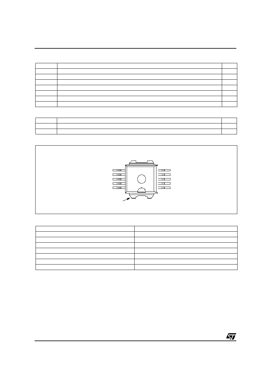
PIN FUNCTION
(*) Pin 1
˜
5=Power GND, Pin 6=signal GND. Pin 6 must be connected to pins 1
˜
5 externally.
No
Name
Function
1
˜
5
GND
Emitter power ground
6(*)
GND
Control ground
7
V
d
Driving stage supply voltage
8
N.C.
9
INPUT
Logic input channel
10
DIAG
Diagnostic output signal (when I
C
is greater than 3A)
TAB
HV
C
Primary coil output signal
1
2
3
4
5
6
7
8
9
10
11
GND
GND
GND
GND
GND
GND
V
d
N.C.
INPUT
DIAG
HV
C

3/7
VB027BSP
ELECTRICAL CHARACTERISTICS
(V
CC
=13.5V; V
d
=5V; Tj=25∫C; R
coil
=510m
;
L
coil
=7mH unless otherwise
specified)
Symbol
Parameter
Test Conditions
Min
Typ
Max
Unit
V
cl
High voltage clamp
-40
∞
C
T
j
125
∞
C; I
C
=6A
320
420
V
V
cg(sat)
Power stage saturation
voltage
I
C
=6A; V
IN
=4V; -40
∞
C
T
j
125
∞
C
2
V
I
d(off)
Power-off supply current
V
IN
=0.4V
11
mA
I
d(on)
Power-on supply current
V
IN
=4V; I
C
=6A; -40
∞
C
T
j
125
∞
C
160
mA
V
d
Driving stage supply
voltage
4.5
5.5
V
I
cl
Collector current limit
V
IN
=4V
8.5
10.5
A
I
cl(td)
Collector current limit drift
with temperature
See figure 3
I
leak
Collector leakage current
V
c
=125V
100
µ
A
V
INH
High level input voltage
4
5.5
V
V
INL
Low level input voltage
0
0.8
V
I
INH
High level input current
200
µ
A
V
diagH
High level diagnostic
output voltage
R
EXT
=15K
;
C
EXT
=1nF (See figure 1)
3.5
V
d
V
V
diagL
Low level diagnostic
output voltage
R
EXT
=22K
;
C
EXT
=1nF (See figure 1)
0.5
V
I
C(diag1)
First threshold level
collector current
4.25
4.5
4.75
A
I
C(diag1)td
First threshold level
collector current drift with
temperature
See figure 4
I
C(diag2)
Second threshold level
collector current
5.45
5.8
6.15
A
I
C(diag2)td
Second threshold level
collector current drift with
temperature
See figure 5
I
diagH
Overtemperature
diagnostic current
2
2.6
3.2
A
t
d(off)
Turn-off delay time of
output current
I
C
=6A
5
25
45
µ
s
t
f(off)
Turn-off fall time of output
current
I
C
=6A
2
8
15
µ
s
E
s/b
Single pulse avalanche
energy
300
mJ
T
int
Temperature ofdiagnostic
shift
130
150
170
∞
C
T
hys
Thermal hysteresis
30
∞
C
V
f
Diode forward voltage
I
C
= -10A
3
V
1

4/7
VB027BSP
PRINCIPLE OF OPERATION
The VB027BSP is mainly intended as high voltage power
switch device driven by a logic level input and interfaces
directly to a high energy electronic ignition coil.
The input V
IN
of the VB027BSP is fed from a low power
signal generated by an external controller that determines
both dwell time and ignition point. During V
IN
high (
4V)
the VB027BSP increases current in the coil to the desired,
internally set current level.
When the collector current exceeds 4.5A, the diagnostic
signal is turned high and it remains so, until the load
current reaches 5.8A (second threshold). At that value,
the diagnostic signal is turned low, and the
µ
C forces the
V
IN
to the low state. During the coil current switch-off, the
primary voltage HV
C
is clamped by a series of Zener
diodes at an internally set value V
cl
typically 365V.
The collector current sensed through the R
sense
, is limited
thanks to the "Current limiter" block that, as soon as the I
cl
level is reached, forces the darlington (using the "Driver"
block) to limit the current provided.
The transition from saturation to desaturation, coil current
limiting phase, must have the ability to accommodate an
overvoltage. A maximum overshoot of 20V is allowed.
There can be some short period of time in which the
output pin (HV
C
) is pulled below ground by a negative
current
due
to
leakage
inductances
and
stray
capacitances of the ignition coil. This can cause parasitic
glitches on the diagnostic output. VB027BSP has a built-
in protection circuit that allows to lock the p-buried layer
potential of the linear stage to the collector power, when
the last one is pulled underground.
THERMAL BEHAVIOUR
You can see in the block diagram of the VB027BSP a box
called overtemperature protection. The purpose of this
circuit is to shift the current level at which the first
diagnostic is activated down to about 2.5A.
This information can be managed by the micro that can
take the corrective action in order to reduce the power
dissipation. This block is not an effective protection but
just an overtemperature detection. The shift down of the
first flag level cannot be present for temperatures lower
than 125
∞
C.
As an example of its behavior you can suppose a very
simple motor management system in which the micro
does just a simple arithmetic calculation to decide when to
switch-off the device after the first flag threshold.
EXAMPLE:
I
C(DIAG1)
info after x ms (I
C(DIAG1)
=4.5A)
I
switch-off
info after kx ms.
As soon as the temperature rises over the overtemp
threshold, the first diagnostic is shifted down to about
2.5A and, in this example, the switch-off current will be
kx*2.5 / 4.5.
OVERVOLTAGE
The VB027BSP can withstand the following transients of
the battery line:
-100V / 2ms (R
i
=10
)
+100V / 0.2ms (R
i
=10
)
+50V / 400ms (R
i
=4.2
,
with V
IN
=3V)
FIGURE 1: Application circuit

5/7
VB027BSP
1
FIGURE 2: Switching waveform
FIGURE 3:
Maximum
I
cl
VS temperature
FIGURE 5: I
C(diag2)
VS temperature
FIGURE 4: I
C(diag1)
VS temperature
FIGURE 6: V
cg(sat)
VS temperature (at I
C
=6A)
1
V
IN
2
nd
Threshold
1
st
Threshold
I
cl
DIAG
-40
25
125
Temperature [
∞
C]
1.1
1.2
1.3
1.4
1.5
1.6
1.7
[V]
max
Avg
min