VN30N
HIGH SIDE SMART POWER SOLID STATE RELAY
PRELIMINARY DATA
s
OUTPUT CURRENT (CONTINUOUS): 45A @
T
c
=25
o
C
s
5V LOGIC LEVEL COMPATIBLE INPUT
s
THERMAL SHUT-DOWN
s
UNDER VOLTAGE SHUT-DOWN
s
OPEN DRAIN DIAGNOSTIC OUTPUT
s
VERY LOW STAND-BY POWER
DISSIPATION
DESCRIPTION
The VN30N is a monolithic device made using
SGS-THOMSON
Vertical
Intelligent
Power
Technology, intended for driving resistive or
inductive loads with one side grounded.
Built-in thermal shut-down protects the chip from
over temperature and short circuit.
The input control is 5V logic level compatible.
The open drain diagnostic output indicates open
circuit (no load) and over temperature status.
September 1994
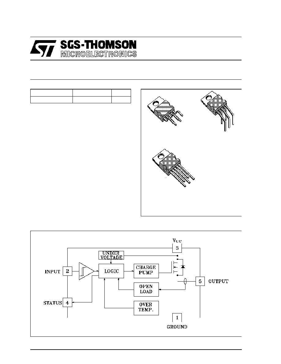
BLOCK DIAGRAM
TYPE
V
DSS
R
DS ( on)
I
OUT
V
C C
VN30N
60 V
0.03
45 A
26 V
PENTAWATT
(vertical)
PENTAWATT
(horizontal)
PENTAWATT
(in-line)
ORDER CODES:
PENTAWATT vertical
VN30N
PENTAWATT horizontal
VN30N (011Y)
PENTAWATT in-line
VN30N (012Y)
1/10

ABSOLUTE MAXIMUM RATING
Symbol
Parameter
Value
Uni t
V
( BR)DSS
Drain-Source Breakdown Voltage
60
V
I
O UT
Output Current (cont.)
45
A
I
R
Reverse Output Current
-45
A
I
I N
I nput Current
±
10
mA
-V
CC
Reverse Supply Voltage
-4
V
I
STA T
St atus Current
±
10
mA
V
E SD
Electrost atic Discharge (1.5 k
, 100 pF)
2000
V
P
tot
Power Dissipat ion at T
c
25
o
C
108
W
T
j
Junction Operating Temperature
-40 to 150
o
C
T
stg
St orage Temperat ure
-55 to 150
o
C
CONNECTION DIAGRAM
CURRENT AND VOLTAGE CONVENTIONS
VN30N
2/10

THERMAL DATA
R
thj-cas e
R
thj- amb
Thermal Resist ance Junct ion-case
Max
Thermal Resist ance Junction-ambient
Max
1.15
60
o
C/ W
o
C/ W
ELECTRICAL CHARACTERISTICS (V
CC
= 13 V; -40
T
j
125
o
C unless otherwise specified)
POWER
Symbol
Parameter
Test Condi tions
Mi n.
Typ.
Max.
Unit
V
C C
Supply Voltage
7
26
V
R
on
On St ate Resist ance
I
OU T
= 18 A
I
OU T
= 18 A
T
j
= 25
o
C
0. 06
0. 03
I
S
Supply Current
Of f State
T
j
25
o
C
On St ate
50
15
µ
A
mA
SWITCHING
Symbol
Parameter
Test Condi tions
Mi n.
Typ.
Max.
Unit
t
d(on)
Turn-on Delay Time Of
Output Current
I
OU T
= 18 A Resistive Load
I nput Rise Time < 0.1
µ
s
T
j
= 25
o
C
30
µ
s
t
r
Rise Time Of Output
Current
I
OU T
= 18 A Resistive Load
I nput Rise Time < 0.1
µ
s
T
j
= 25
o
C
100
µ
s
t
d(off )
Turn-off Delay Time Of
Output Current
I
OU T
= 18 A Resistive Load
I nput Rise Time < 0.1
µ
s
T
j
= 25
o
C
80
µ
s
t
f
Fall Time Of Output
Current
I
OU T
= 18 A Resistive Load
I nput Rise Time < 0.1
µ
s
T
j
= 25
o
C
40
µ
s
(di/dt)
on
Turn-on Current Slope
I
OU T
= 18 A
I
OU T
= I
OV
0.5
3
A/
µ
s
A/
µ
s
(di/dt)
off
Turn-off Current Slope
I
OU T
= 18 A
I
OU T
= I
OV
3
4
A/
µ
s
A/
µ
s
LOGIC INPUT
Symbol
Parameter
Test Condi tions
Mi n.
Typ.
Max.
Unit
V
IL
I nput Low Level
Voltage
0.8
V
V
IH
I nput High Level
Voltage
2
(*)
V
V
I(hy st.)
I nput Hysteresis
Voltage
0.5
V
I
I N
I nput Current
V
IN
= 5 V
250
500
µ
A
V
ICL
I nput Clamp Voltage
I
IN
= 10 mA
I
IN
= -10 mA
6
-0. 7
V
V
PROTECTIONS AND DIAGNOSTICS
Symbol
Parameter
Test Condi tions
Mi n.
Typ.
Max.
Unit
V
STAT
(
∑
)
St atus Voltage Output
Low
I
STAT
= 1.6 mA
0.4
V
V
US D
Under Voltage Shut
Down
6.5
7
V
VN30N
3/10

ELECTRICAL CHARACTERISTICS (continued)
PROTECTION AND DIAGNOSTICS (continued)
Symbol
Parameter
Test Condi tions
Mi n.
Typ.
Max.
Unit
V
S CL
(
∑
)
St atus Clamp Voltage
I
STAT
= 10 mA
I
STAT
= -10 mA
6
-0. 7
V
V
t
S C
Switch-off Time in
Short Circuit Condition
at Start-Up
R
LOA D
< 10 m
T
c
= 25
o
C
1
ms
I
OV
Over Current
R
LOA D
< 10 m
-40
T
c
125
o
C
140
A
I
AV
Average Current in
Short Circuit
R
LOA D
< 10 m
T
c
= 85
o
C
2.5
A
I
OL
Open Load Current
Level
5
1250
mA
T
TS D
Thermal Shut-down
Temperature
140
o
C
T
R
Reset Temperature
125
o
C
(*) The V
IH
is internally cl amped at 6V about. It is possibl e to connect this pin to an higher voltage via an external resi stor
cal culated to not exceed 10 mA at the i nput pin.
(
∑
) Status deter mination > 100
µ
s after the switching edge.
FUNCTIONAL DESCRIPTION
The device has a diagnostic output which
indicates
open
circuit
(no
load)
and
over
temperature conditions. The output signals are
processed by internal logic.
To protect the device against short circuit and
over-current condition, the thermal protection
turns the integrated Power MOS off at a minimum
junction temperature of 140
o
C. When the
temperature returns to about 125
o
C the switch is
automatically turned on again.
In short circuit conditions the protection reacts
with virtually no delay, the sensor being located in
the region of the die where the heat is generated.
PROTECTING THE DEVICE AGAINST REVER-
SE BATTERY
The simplest way to protect the device against a
continuous reverse battery voltage (-26V) is to
insert a Schottky diode between pin 1 (GND) and
ground, as shown in the typical application circuit
(fig. 3).
The consequences of the voltage drop across
this diode are as follows:
≠
If the input is pulled to power GND, a negative
voltage of -V
F
is seen by the device. (V
IL
, V
IH
thresholds and V
STAT
are increased by V
F
with
respect to power GND).
≠
The undervoltage shutdown level is increased
by V
F
.
If there is no need for the control unit to handle
external analog signals referred to the power
GND, the best approach is to connect the
reference potential of the control unit to node [1]
(see application circuit in fig. 4), which becomes
the common signal GND for the whole control
board.
In this way no shift of V
IH
, V
IL
and V
STAT
takes
place and no negative voltage appears on the
INPUT pin; this solution allows the use of a
standard diode, with a breakdown voltage able to
handle any ISO normalized negative pulses that
occours in the automotive environment.
VN30N
4/10
