�
Mono and Colour Digital Video CMOS Image Sensors
CD5404-6404F-A
1/54
VV5404 & VV6404
DESCRIPTION
VV5404 and VV6404 are highly integrated CMOS VLSI
sensors which enables high standards of performance and
image quality at a very cost-effective price point. The 356 x
292 monochrome device offers one of the simplest routes
currently available to design-in of imaging applications, while
the colour device is ideal for low cost PC camera applications.
Both devices incorporate a comprehensive range of on-board
controls eliminating the need for additional support chips. On-
chip A/D conversion provides 8 bit digital output and the
device set up is fully automatic via the built-in automatic black
level calibration algorithm.
Exposure and gain settings are programmable and operation
is controlled via a serial interface.
This sensors offer variable frame rates of up to 30 frames per
second and a 4 wire digital video bus. The digital interface
also provides a tri-stateable data qualification clock and frame
synchronisation signal.
Hand-held products, in applications such as PDAs, bar code
scanning or automatic meter reading, will benefit from the low
power requirements and from the inbuilt sleep and power
down modes.
The price and performance standards introduced with the
VV5404 and VV6404 enable use of an imaging solution
where previously it may not have been practicable on cost
grounds.
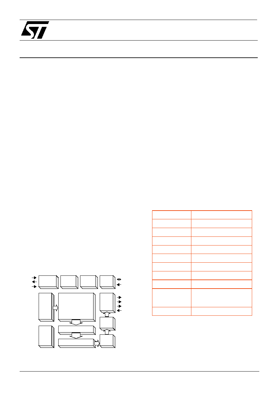
BLOCK DIAGRAM
FEATURES
�
CIF Format mono or colour pixel array
�
Up to 30 frames per second operation
�
On-chip 8 bit analogue to digital converter
�
Low power consumption
�
Up to 356 x 292 pixel image size
�
Automatic exposure and gain control
�
Serial interface control
�
Programmable exposure and gain values
�
Automatic black level calibration
�
4-wire digital video bus
�
Evaluation kit available
APPLICATIONS
�
PC Cameras
�
Biometrics
�
Inspection Systems
SPECIFICATIONS
Important:
1.
A colour co-processor is required to convert the VV6404 sensor's video
data stream of raw colourised pixel data into either a CIF or QCIF for-
mat RGB or YUV colour image.
2.
VV5404 and VV6404 do NOT have any form of automatic exposure
control. This must be performed externally.
SAM PLE & HO LD
HORIZO NTAL SHIFT
PHO TO DIO D E
ANALO G
VO LTAG E
REFS.
SD A
SC L
D[3:0]
VERTICAL
SHIFT
REG ISTER
C LK O
8-bit
ADC
ARRAY
REG ISTER
SERIAL
INTER-
FACE
OUTPUT
FORM AT
GAIN
IM AG E
FO RM AT
BLACK
CALIBRATIO N
EXPO SURE
REG ISTERS
STAG E
O E B
FS T
Q C K
S IN
C LKI
Pixel resolution
356 x 292 (CIF)
Array size
4.272mm x 3.212mm
Pixel size
12.0
�
m x 11.0
�
m
Min. illumination
0.1 lux
Exposure control
Automatic (to 25000:1)
Gain control
Automatic (to +20dB)
Signal/Noise ratio
46dB
Supply voltage
5.0v DC
+/-
5%
Supply current
<75mA
Operating
temperature
(ambient)
0
o
C - 40
o
C
(for extended temp. info please con-
tact STMicroelectronics)
Package type
48LCC

VV5404 & VV6404
CD5404-6404F-A
2/54
Table of Contents
1. Introduction. . . . . . . . . . . . . . . . . . . . . . . . . . . . . . . . . . . . . . . . . . . . . . . . . . . . . . . . . . . 4
2. Operating Modes . . . . . . . . . . . . . . . . . . . . . . . . . . . . . . . . . . . . . . . . . . . . . . . . . . . . . . 6
2.1 Image Read-out Options. . . . . . . . . . . . . . . . . . . . . . . . . . . . . . . . . . . . . . . . . . . . . . . . . 6
2.2 Frame Rate Options . . . . . . . . . . . . . . . . . . . . . . . . . . . . . . . . . . . . . . . . . . . . . . . . . . . . 6
3. Exposure Control . . . . . . . . . . . . . . . . . . . . . . . . . . . . . . . . . . . . . . . . . . . . . . . . . . . . . . 8
4. Digital Video Interface Format. . . . . . . . . . . . . . . . . . . . . . . . . . . . . . . . . . . . . . . . . . . . 9
4.1 General description. . . . . . . . . . . . . . . . . . . . . . . . . . . . . . . . . . . . . . . . . . . . . . . . . . . . . 9
4.2 Embedded control data. . . . . . . . . . . . . . . . . . . . . . . . . . . . . . . . . . . . . . . . . . . . . . . . . .9
4.2.1 The combined escape and sync character . . . . . . . . . . . . . . . . . . . . . . . . . . . . . . . . . 9
4.2.2 The command word . . . . . . . . . . . . . . . . . . . . . . . . . . . . . . . . . . . . . . . . . . . . . . . . . . . 9
4.2.3 Supplementary Data . . . . . . . . . . . . . . . . . . . . . . . . . . . . . . . . . . . . . . . . . . . . . . . . .13
4.3 Video timing reference and status/configuration data. . . . . . . . . . . . . . . . . . . . . . . . . . 13
4.3.1 Blank lines . . . . . . . . . . . . . . . . . . . . . . . . . . . . . . . . . . . . . . . . . . . . . . . . . . . . . . . . . 14
4.3.2 Black line timing . . . . . . . . . . . . . . . . . . . . . . . . . . . . . . . . . . . . . . . . . . . . . . . . . . . . . 14
4.3.3 Valid video line timing . . . . . . . . . . . . . . . . . . . . . . . . . . . . . . . . . . . . . . . . . . . . . . . . 14
4.3.4 Start of frame line timing . . . . . . . . . . . . . . . . . . . . . . . . . . . . . . . . . . . . . . . . . . . . . . 14
4.3.5 End of frame line timing . . . . . . . . . . . . . . . . . . . . . . . . . . . . . . . . . . . . . . . . . . . . . . .14
4.4 Detection of sensor using data bus state . . . . . . . . . . . . . . . . . . . . . . . . . . . . . . . . . . .14
4.5 Resetting the Sensor Via the Serial Interface. . . . . . . . . . . . . . . . . . . . . . . . . . . . . . . . 14
4.6 Power-up, Low-power and Sleep modes . . . . . . . . . . . . . . . . . . . . . . . . . . . . . . . . . . .14
4.6.1 Power-Up/Down (Figure 12) . . . . . . . . . . . . . . . . . . . . . . . . . . . . . . . . . . . . . . . . . . . 18
4.6.2 Low-Power Mode (Figure 10) . . . . . . . . . . . . . . . . . . . . . . . . . . . . . . . . . . . . . . . . . .18
4.6.3 Sleep Mode (Figure 11) . . . . . . . . . . . . . . . . . . . . . . . . . . . . . . . . . . . . . . . . . . . . . . .18
4.6.4 Application of the system clock during sensor low-power modes . . . . . . . . . . . . . . . 22
4.7 Qualification of Output Data . . . . . . . . . . . . . . . . . . . . . . . . . . . . . . . . . . . . . . . . . . . . . 22
4.7.1 Using the External Clock signal applied to CKI . . . . . . . . . . . . . . . . . . . . . . . . . . . . . 22
4.7.2 Data Qualification Clock, QCK. . . . . . . . . . . . . . . . . . . . . . . . . . . . . . . . . . . . . . . . . .22
4.7.3 Frame Start Signal, FST . . . . . . . . . . . . . . . . . . . . . . . . . . . . . . . . . . . . . . . . . . . . . . 22
5. Serial Control Bus . . . . . . . . . . . . . . . . . . . . . . . . . . . . . . . . . . . . . . . . . . . . . . . . . . . . 27
5.1 General Description . . . . . . . . . . . . . . . . . . . . . . . . . . . . . . . . . . . . . . . . . . . . . . . . . . . 27
5.2 Serial Communication Protocol . . . . . . . . . . . . . . . . . . . . . . . . . . . . . . . . . . . . . . . . . .27
5.3 Data Format. . . . . . . . . . . . . . . . . . . . . . . . . . . . . . . . . . . . . . . . . . . . . . . . . . . . . . . . . 27
5.4 Message Interpretation . . . . . . . . . . . . . . . . . . . . . . . . . . . . . . . . . . . . . . . . . . . . . . . . .28
5.5 The Programmers Model . . . . . . . . . . . . . . . . . . . . . . . . . . . . . . . . . . . . . . . . . . . . . . .29
5.5.1 DeviceH [000_00002] and DeviceL [000_ 00012] . . . . . . . . . . . . . . . . . . . . . . . . . . . 31
5.5.2 Status0 [000_00102] . . . . . . . . . . . . . . . . . . . . . . . . . . . . . . . . . . . . . . . . . . . . . . . . .31
5.5.3 Line_count_H [000_00112] & Line_count_L [000_01002]. . . . . . . . . . . . . . . . . . . . . 31
5.5.4 Setup0 [001_00002] . . . . . . . . . . . . . . . . . . . . . . . . . . . . . . . . . . . . . . . . . . . . . . . . .32
5.5.5 Setup1 [001_00012] . . . . . . . . . . . . . . . . . . . . . . . . . . . . . . . . . . . . . . . . . . . . . . . . .32
5.5.6 Setup2 [001_00102] . . . . . . . . . . . . . . . . . . . . . . . . . . . . . . . . . . . . . . . . . . . . . . . . .33
5.5.7 Setup4 [001_01002] . . . . . . . . . . . . . . . . . . . . . . . . . . . . . . . . . . . . . . . . . . . . . . . . .33
5.5.8 Setup5 [001_01012] . . . . . . . . . . . . . . . . . . . . . . . . . . . . . . . . . . . . . . . . . . . . . . . . .34
5.5.9 Exposure Control Registers [010_00002] - [010_10012]. . . . . . . . . . . . . . . . . . . . . . 35
5.5.10 ADC Setup Register AS0 [111_01112] . . . . . . . . . . . . . . . . . . . . . . . . . . . . . . . . . . 37
5.6 Types of messages. . . . . . . . . . . . . . . . . . . . . . . . . . . . . . . . . . . . . . . . . . . . . . . . . . . . 38
5.6.1 Single location, single data write. . . . . . . . . . . . . . . . . . . . . . . . . . . . . . . . . . . . . . . . 38

VV5404 & VV6404
CD5404-6404F-A
3/54
5.6.2 Single location, single data read.. . . . . . . . . . . . . . . . . . . . . . . . . . . . . . . . . . . . . . . .38
5.6.3 No data write followed by same location read. . . . . . . . . . . . . . . . . . . . . . . . . . . . . . 38
5.6.4 Same location multiple data write. . . . . . . . . . . . . . . . . . . . . . . . . . . . . . . . . . . . . . . . 39
5.6.5 Same location multiple data read . . . . . . . . . . . . . . . . . . . . . . . . . . . . . . . . . . . . . . . 39
5.6.6 Multiple location write . . . . . . . . . . . . . . . . . . . . . . . . . . . . . . . . . . . . . . . . . . . . . . . . 40
5.6.7 Multiple location read. . . . . . . . . . . . . . . . . . . . . . . . . . . . . . . . . . . . . . . . . . . . . . . . .40
5.7 Serial Interface Timing . . . . . . . . . . . . . . . . . . . . . . . . . . . . . . . . . . . . . . . . . . . . . . . . .41
6. Clock Signal . . . . . . . . . . . . . . . . . . . . . . . . . . . . . . . . . . . . . . . . . . . . . . . . . . . . . . . . . 42
6.8 Synchronising 2 or More Cameras . . . . . . . . . . . . . . . . . . . . . . . . . . . . . . . . . . . . . . . .43
7. Detailed specifications. . . . . . . . . . . . . . . . . . . . . . . . . . . . . . . . . . . . . . . . . . . . . . . . .45
7.1 General . . . . . . . . . . . . . . . . . . . . . . . . . . . . . . . . . . . . . . . . . . . . . . . . . . . . . . . . . . . . .45
7.2 DC characteristics. . . . . . . . . . . . . . . . . . . . . . . . . . . . . . . . . . . . . . . . . . . . . . . . . . . . . 45
8. Physical . . . . . . . . . . . . . . . . . . . . . . . . . . . . . . . . . . . . . . . . . . . . . . . . . . . . . . . . . . . . .46
8.1 Pinout Diagram . . . . . . . . . . . . . . . . . . . . . . . . . . . . . . . . . . . . . . . . . . . . . . . . . . . . . . . 46
8.2 Signal Names . . . . . . . . . . . . . . . . . . . . . . . . . . . . . . . . . . . . . . . . . . . . . . . . . . . . . . . .47
8.3 48LCC Mechanical Dimensions . . . . . . . . . . . . . . . . . . . . . . . . . . . . . . . . . . . . . . . . . .49
8.4 VV6404 Sensor Support Circuit Schematic Diagram . . . . . . . . . . . . . . . . . . . . . . . . . . 50
8.5 Sensor Support Circuit Component List . . . . . . . . . . . . . . . . . . . . . . . . . . . . . . . . . . .50
9. Ordering Information . . . . . . . . . . . . . . . . . . . . . . . . . . . . . . . . . . . . . . . . . . . . . . . . . . 52
VV5404 & VV6404
CD5404-6404F-A
4/54
1.
Introduction
VV5404 and VV6404 are CIF format CMOS image sensors capable of outputing digital pixel data at frame rates, of
upto 30 frames per second. The VV5404 is a monochrome part, while the VV6404 has a colour filter applied over the
sensor array.
Important: The VV6404 sensor's video data stream only contains raw colourised pixel data. A colour co-processor
is required to generate for example either a CIF or a QCIF format YUV colour image.
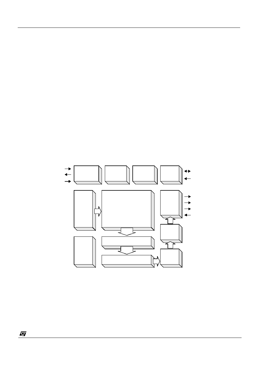
The 356 x 292 pixel sensors have an on-chip 8-bit analogue to digital converter (Figure 1). The sensors offer very
flexible digital interface, the main components of which are listed below:
1. A tri-stateable 4-wire data bus (D[3:0]) for sending both video data and embedded timing references.
2. A data qualification clock, QCK, which can be programmable via the serial interface to behave in a number of
different ways (Tri-stateable).
3. A frame start signal, FST (Tri-stateable).
4. A 2-wire serial interface (SDA,SCL) for controlling and setting up the device.
5. The ability to synchronise the operation of multiple cameras - synchronisation input, SIN.
An 8-bit pixel value is transmitted across the 4 wire tri-stateable databus as series pair of 4-bit nibbles, most significant
nibble first. Along within the pixel data, codes representing the start and end frames and the start and end of lines are
embedded within the video data stream to allow the video processor to synchronise with video data the camera
module is generating. Section 4. defines the format for the output video datastream.
To complement the embedded control sequences a data qualification clock, QCK, and a frame start signal are also
available. QCK can be set-up to either be:
1. Disabled
2. Free-running.
3. Qualify only the control sequences and the pixel data.
4. Qualify the pixel data only
There is also the choice of two different QCK frequencies, where one is twice the frequency of the other.
SAMPLE & HOLD
HORIZONTAL SHIFT
PHOTO DIODE
ANALOG
VOLTAGE
REFS.
SDA
SCL
D[3:0]
VERTICAL
SHIFT
REGISTER
CLKO
8-bit
ADC
ARRAY
REGISTER
SERIAL
INTER-
FACE
Figure 1 : Block Diagram of VV5404 and VV6404 Image Sensors
OUTPUT
FORMAT
GAIN
IMAGE
FORMAT
BLACK
CALIBRATION
EXPOSURE
REGISTERS
STAGE
OEB
FST
QCK
SIN
CLKI
VV5404 & VV6404
CD5404-6404F-A
5/54
1. Fast QCK: the falling edge of the clock qualifies the nibble data irrespective of whether it is the most or the least
significant nibble.
2. Slow QCK: the rising edge of the clock qualifies the most significant nibbles while the falling edge of the clock
qualifies the least significant nibbles.
The FST can be enabled/disabled via the serial interface.
OEB tri-states all 4 databus lines, D[3:0], the qualification clock, QCK and the frame start signal, FST.
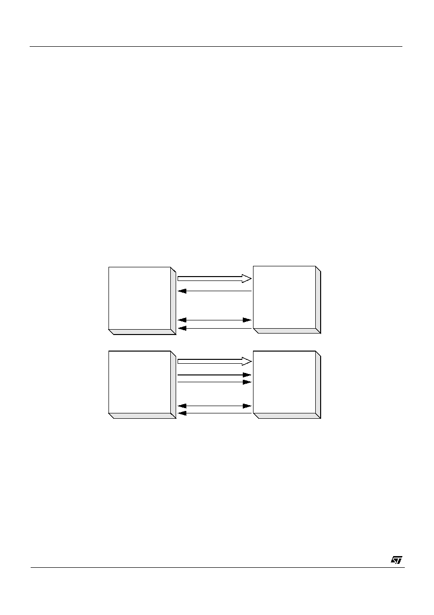
There are 3 main ways of interfacing to the VV5404 or VV6404 sensor based on the above signals:
1. The processor capturing the data (or colour co-processor for VV6404) supplies the sensor clock, CKI, and uses
the embedded control sequences to synchronise with the frame and line level timings. Thus the processor and
sensor are running off derivatives of the same fundamental clock (4 fsc - 14.31818 MHz). To allow the receiver
to determine the best sampling position of the video data, during its power-up sequence the sensor outputs a
101010... sequence on each of its databus lines for the video processor to lock on to.
2. The video processor uses a free-running QCK supplied by the sensor to sample the incoming video data
stream. The embedded control sequences are used to synchronise the frame and line level timings. A crystal is
used to generate the clock for the sensor.
3. The video processor uses FST and the data only mode for QCK to synchronise to the incoming video data. Pri-
marily intended for interfacing to frame grabbers.
The 2-wire serial interface provides complete control over how the sensor is setup and run. Exposure and gain values
are programmed via this interface. Section 5. defines the communications protocol and the register map of all the
locations which can be accessed via the serial interface.
Using the first two interface options outlined above it is possible to control the sensor and receive video data via a 9-
wire cable between the sensor and the video processor/colour-processor.
1. A 4-wire data bus (D[3:0]) for sending both video data and embedded timing references.
2. A 2-wire serial interface (SDA,SCL).
3. The clock for the sensor or QCK from the sensor.
4. VCC and GND power lines.
The various image read-out and frame rate options are detailed in Sections 2 and 3 respectively.
Figure 2 : Interfacing Options
SDA
SCL
D[3:0]
CLKI
Sensor
Colour
Co-processor
(processor)
SDA
SCL
D[3:0]
QCK
Sensor
Colour
Co-processor
(processor)
FST