 | –≠–ª–µ–∫—Ç—Ä–æ–Ω–Ω—ã–π –∫–æ–º–ø–æ–Ω–µ–Ω—Ç: WARP11 | –°–∫–∞—á–∞—Ç—å:  PDF PDF  ZIP ZIP |
W.A.R.P. 1.1
WEIGHT ASSOCIATIVE RULE PROCESSOR
ADVANCED DATA
High Speed Rules Processing
Antecedent Membership Functions with any
Shape
Up to 256 Rules (4 Antecedents,1
Consequent)
Up to 16 Input Configurable Variables
Up to 16 Membership Functions for an Input
Variable
Up to 16 Output Variables
Up to 128 Membership Functions for all
Consequents
MAX-DOT Inference Method
Defuzzification on chip
Software Tools and Emulators Availability
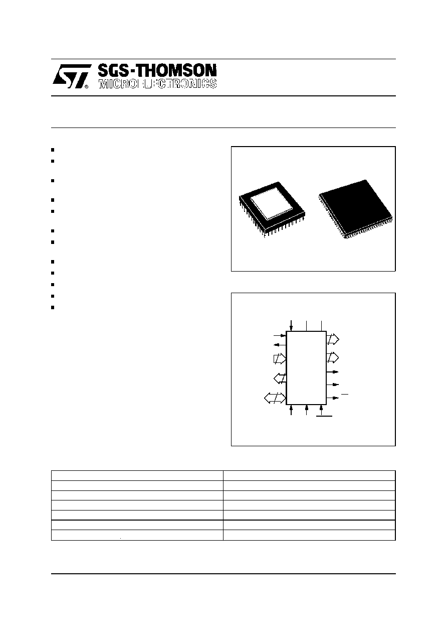
100-pin CPGA100 Ceramic Package
84-lead Plastic Leaded Chip Carrier package
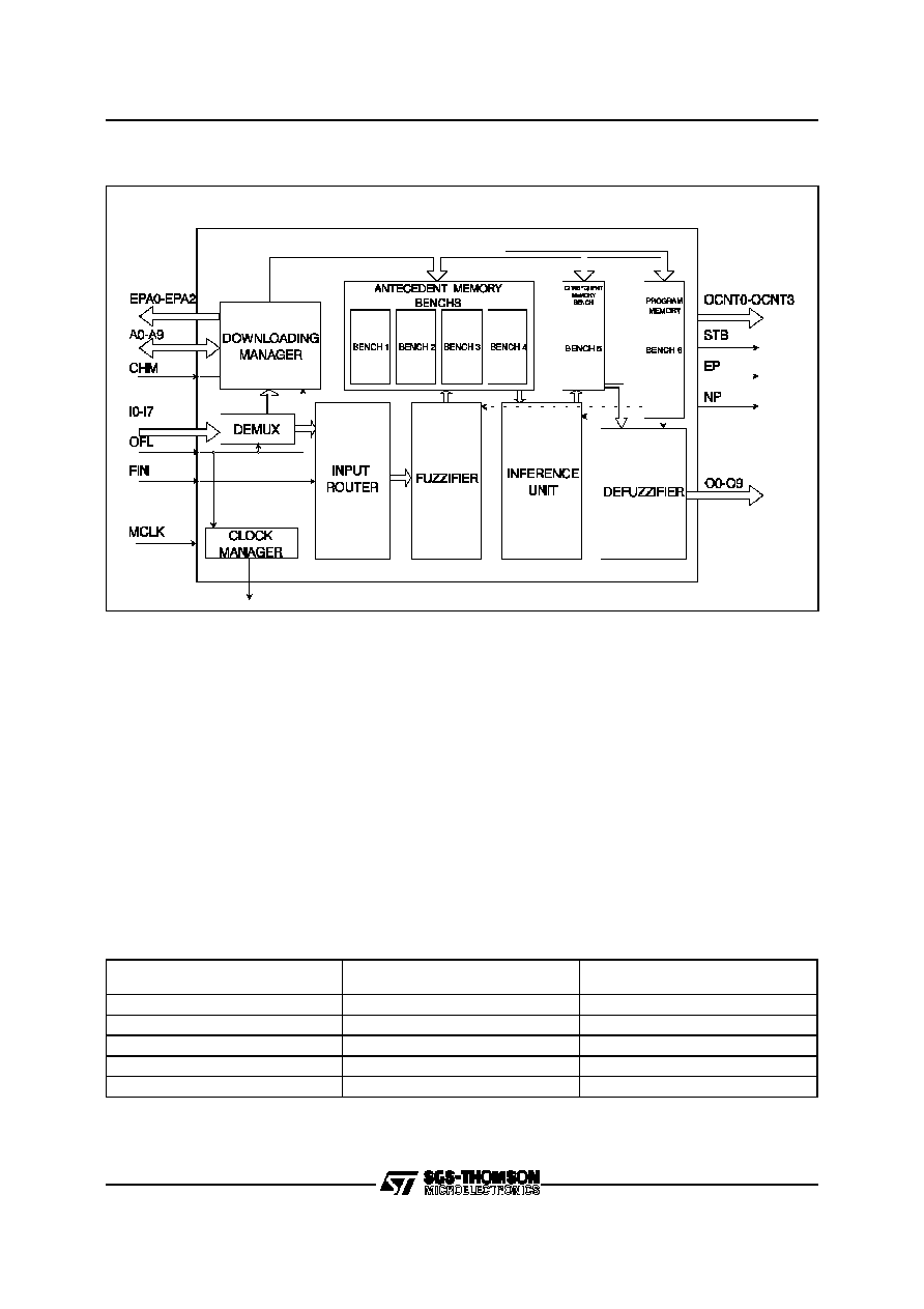
GENERAL DESCRIPTION
W.A.R.P. is a VLSI Fuzzy Logic controller whose
architecture arises from the need of realizing an
integrated structure with high inferencing perform-
ances and flexibility. To get those results a modular
architecture based on a set of parallel memory
blocks has been implemented.
In order to obtainhigh performances W.A.R.P. uses
different data representations during the various
phases of the computational cycle, so that it is
always operating on the optimal data repre-
sentation. A vectorial characterization has been
adopted for the Antecedent Membership Func-
tions. W.A.R.P. exploits a SGS-THOMSON pat-
ented strategy to store the Antecedent Membership
May 1996
This is advance information on a new product now in development or undergoing evaluation. Details are subject to change without no tice.
8
I0-I7
A0-A9
10
O0-O9
FIN
3
CHM OFL
4
OCNT0-OCNT3
STB
EP
NP
PRS T
MCLK VS S VDD
W.A.R.P.
1.1
10
EPA0-EPA2
S YNC
Figure 1. Logic Diagram
Number of Inputs
Configurable [1..8]
Standard Rule Format
4 Antecedents, 1 Consequent [or subsets]
Rules Number
Max 256 Rules in the 4 Antecedent, 1 Consequent format
Antecedent's MFs Number
Configurable [up to 16 for an input variable]
Consequent's MFs Number
Max 256 for all outputs variables
Input Data Resolution
8 bit
Output Data Resolution
8 bit
Table 1. W.A.R.P. Configuration Settings
CPGA 100
PLCC84
1/19

Symbol
Parameter
Value
Unit
V
DD
Supply Voltage
-0.5 to 7
V
V
I
Input Voltage
-0.5 to V
DD
+0.5
V
V
O
Ouput Voltage
-0.5 to V
DD
+0.5
V
I
OL
Output Sink Peak Current
+24
mA
I
OH
Output Source Peak Current
-12
mA
T
OPT
Operating Temperature
0 to +70
∞
C
T
STG
Storage Temperature (Ceramic)
-65 to +150
∞
C
Storage Temperature (Plastic)
-45 to +125
∞
C
Table 2. Absolute Maximum Ratings
Notes:
Stresses above those listed in the Table "Absolute Maximum Ratings" may cause permanent damage to the device.
These are stress ratings only and operation of the device at these or any other conditions above those indicated in the Operating
sections of this specification is not implied. Exposure to Absolute Maximum Rating conditions for extended periods may affect
device reliability. Refer also to the SGS-THOMSON SURE Program and other relevant quality documents.
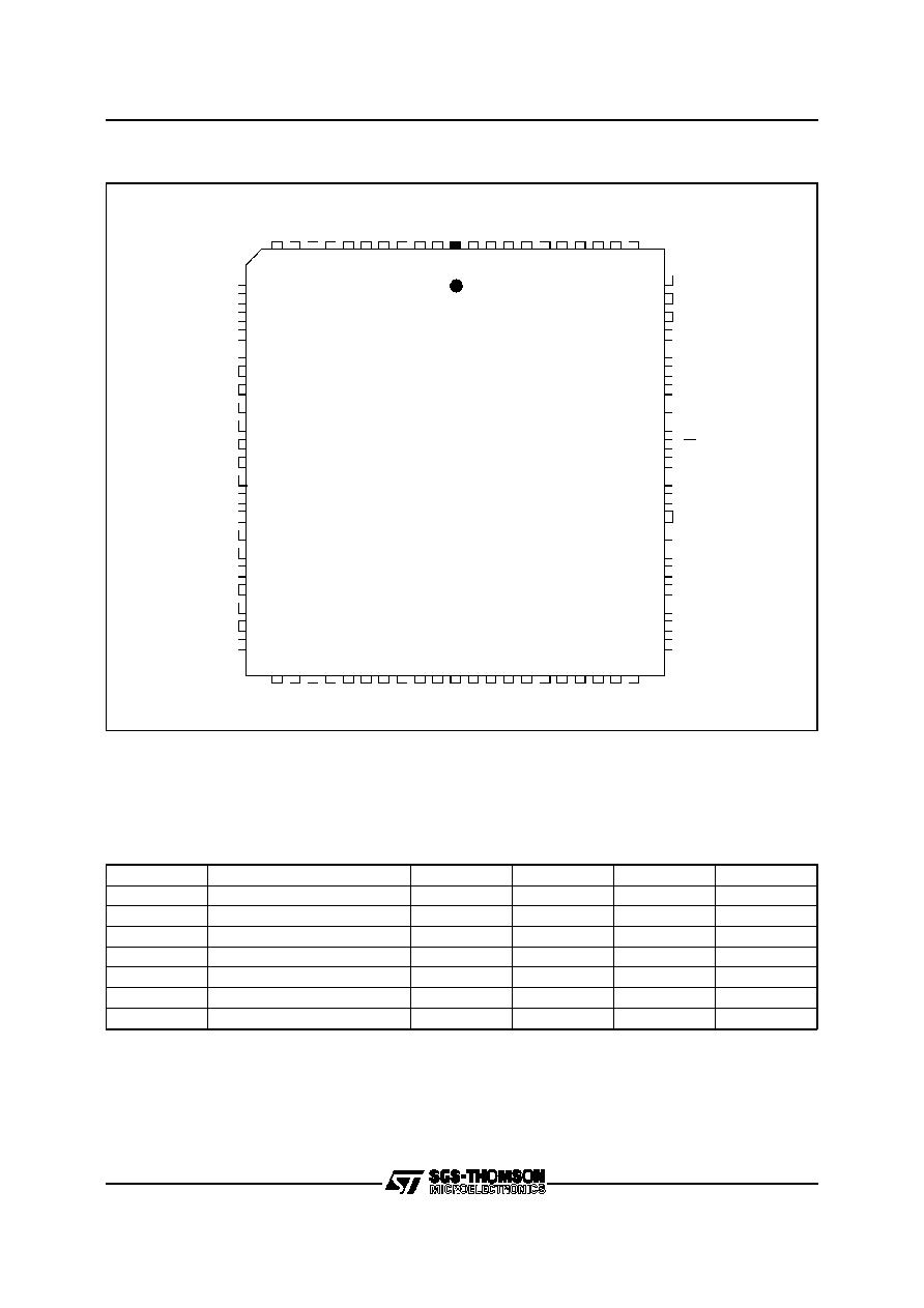
Figure 2. CPGA100 Pin Configuration
2/19
W.A.R.P.1.1
VSS
VDD
MCLK
I0
I1
I2
I3
I4
I5
I6
I7
CHM
FIN
OFL
PRST
TE
MTE
VSS
VDD
VSS
VDD
O0
O1
O2
O3
O4
VSS
O5
O6
O7
O8
O9
VDD
VSS
VDD
VSS
A0
A1
A2
A3
A4
VDD
VSS
EPA0
EPA1
EPA2
A5
A6
A7
A8
A9
VDD
VSS
VDD
VSS
SYNC
OTST
OMTS
STB
EP
VSS
NP
OCNT3
OCNT2
OCNT1
OCNT0
VSS
VDD
74
73
72
71
70
69
68
67
66
65
64
63
62
61
60
59
58
57
56
55
54
33 34 35 36 37 38 39 40 41 42 43 44 45 46 47 48 49 50 51 52 53
12
13
14
15
16
17
18
19
20
21
22
23
24
25
26
27
28
29
30
31
32
11 10 9
8
7
6
5
4
3
2
1 84 83 82 81 80 79 78 77 76 75
W.A.R.P. 1.1
Figure 3. PLCC84 Pin Configuration
Symbol
Parameter
Min
Typ
Max
Unit
V
DD
Supply Voltage
4.75
5.0
5.25
V
V
IL
Input Voltage
0.8
V
V
IH
Input Voltage
2
V
V
OL
Ouput Voltage
0.5
V
V
OH
Ouput Voltage
2.4
V
FCLK
Clock Frequency
40
MHz
CL
Output Load Capacitance
10
85
pF
Table 3. Recomended Operation Conditions (Ta=0 to +70
∞
C unless otherwise specified)
3/19
W.A.R.P.1.1

Functions in dedicated memories in order to reduce
the computational time. Therefore a great amount
of W.A.R.P. processing is based on a look-up table
approach rather than on on-line calculation.
Those Membership Functions (MFs), each one
portrayed by a configurable resolution of 2
6
or 2
7
elements, are stored in four internal RAMs (1Kbyte
each). The consequent MFs, due to the different
modelling, are loaded in a single RAM by storing
for each MF its area and its barycentre. This is due
to the adoption of the Center of Gravity defuzzifica-
tion method.
The downloading phase allows the setting of the
device, in terms of I/O number, universes of dis-
course and MF shapes. During this phase W.A.R.P.
prepares its internal memories for the on-line
elaboration phase and loads the microcode in its
program memory. This microcode, which drives the
on-line phase, is generated by the Compiler (see
W.A.R.P.-SDT User Manual) according to the
adopted configuration. The possible configurations
are shown in table 1.
During the on-line phase (up to 40MHz working
frequency), W.A.R.P. processes the input data and
produces its outputs according to the configuration
loaded in the downloading phase.
W.A.R.P. is conceived to work together with tradi-
Name
Pins Type
Function
V
DD
-
Power Supply
V
SS
-
Ground
A0-A9
I/O
Memory Address Bus
I0-I7
I
Data Input Bus
PRST
I
Preset
FIN
I
First Input Signal
OFL
I
Off-Line/On-Line Switch
CHM
I
Charge Mode Switch
TE
I
Testing (it must be connected to V
SS
)
MTE
I
Testing (it must be connected to V
SS
)
MCLK
I
Clock (up to 40 MHz)
EPA0-EPA2
*
O
EPROM Address Bus
O0-O9
O
Defuzzified Output
OCNT0-OCNT3
O
Output Counter
STB
O
Strobe (Output Ready Signal)
EP
O
End Process
NP
O
New Process
OTST
O
Testing (it must be connected to V
SS
)
OMTS
O
Testing (it must be connected to V
SS
)
SYNC
O
External Synchronization
Table 4. Pin Description
tional microcontrollers which shall perform normal
control tasks while W.A.R.P. will be indipendently
responsible for all the fuzzy related computing.
W.A.R.P. is manufactured using the high perform-
ance, reliable HCMOS4T (O.7
µ
m) SGS-THOM-
SON Microelectronics process.
PIN DESCRIPTION
V
DD
, V
SS
: Power is supplied to W.A.R.P. using
these pins. V
DD
is the power connection and V
SS
is
the ground connection; multi-connections are nec-
essary.
A0-A9: When the CHM pin is low they accept as
input the addresses for the internal memory bus. In
the off-line mode they are used to address W.A.R.P.
memories where the microprogram and data of
antecedent and consequentmembership functions
must be loaded.
Each A0-A9 word is composed by assembling the
data contained in the memory support related to .cs
and .add files (see W.A.R.P.-SDT User Manual). In
particular, couples of data respectively coming from
.cs and .add files are joined to form a single A0-A9
word in the following way:
*
Pins not used in W.A.R.P. 1.0
4/19
W.A.R.P.1.1

A0
This resulting word allows to identify the appropri-
ate memory [cs2-cs0] and its respective address
[add6-add0] where the relative I0-I7 are to be
stored.
When the CHM pin is high, during the off-line
phase, W.A.R.P. generates the addresses for its
internal memories and send those addresses to the
single external memory support where data (.dat
file) are located. These addresses, which are sent
by means of the EPA0-EPA2 and A0-A9 (EPA0
MSB, A9 LSB) output pins, allow to identify the
data (on the EPROM) that have be loaded in
W.A.R.P. internal memories.
In on-line mode A0-A9 are not used.
I0-I7: During the off-line phase these 8 data input
pins accept the microcode configuration and data
to be written into the internal memories. The ante-
cedent memory word size is 64 bits, so it is neces-
sary to give each word 8 bits at a time. In the same
way are written the words of consequent memory
and of program memory.
In on-line mode this bus carries the input variables
to W.A.R.P.. Input values have a resolution of 6 or
7 bits in accordance with the configuration setting.
PRST: This is the restart pin of W.A.R.P.. It is
possible to restart the work during the computation
(on-line phase) or before the writing of internal
memories (off-line phase). In both cases it must be
put low at least for a clock period.
FIN: During the on-line phase it will start the run-
time acquisition cycle. This pin is activated by
providing a positive pulse for a time no lower than
an entire clock period. When all expected inputs
have been processed, a new FIN pulse must be
sent to activate a new process.
OFL: When this pin is high, the chip is enabled to
load data in the internal RAMs (off-line phase). It
must be low when the fuzzy controller is waiting for
input values and during the processing phase (on-
line phase).
CHM: This pin, which is used only during the off-line
phase, determines the charge mode. CHM is not
present in W.A.R.P. 1.0 release.
When CHM is low the addresses of the internal
memory locations where data have to be stored
must be sent to W.A.R.P. from the outside by
means of the input pins A0-A9.
When CHM is high W.A.R.P. automatically gener-
ates the addresses of its internal memories and
manages the EPROMs reading by means of the
addresses contained in EPA0-EPA2 and A0-A9
output pins (13 bits).
TE: For testing purpose only. It must be connected
to V
SS
.
MTE: For testing purpose only. It must be con-
nected to V
SS
.
MCLK: This is the input master clock whose fre-
quency can reach up to 40MHz (MAX).
During the off-line phase with CHM high, the
DCLK signal with a frequency of MCLK/32 is gen-
erated in order to drive the downloading phase
timing.
EPA0-EPA2: During the off-line phase and in cor-
respondencewith CHM high, these output pins are
joined (as MSB) to A0-A9 to obtaine the complete
address of the memory support where to read the
data to be loaded in W.A.R.P. internal memories.
EPA0-EPA2 are not used when CHM is low or in
W.A.R.P. 1.0 release.
O0-O9: These pins carry out the output values.
When the STB (strobe pin) is high, one output
variable can be read by external devices (in on-line
mode). The resolution of output variables is 1024
points (10 bits). If there are more than one output,
the output variables are calculated one by one and
they are provided in the sequence stabilized during
the editing phase (see W.A.R.P.-SDT User Man-
ual).
OCNT0-OCNT3: This 4 bit output bus provides the
output variables with a progressive number during
the on-line phase. As a consequenceit is possible
to know to which variable correspond the data that
are on the output data bus (O0-O9). The dimension
of OCNT bus is connected with the maximum
number of output variables (16).
STB: The strobe pin enables the user to utilize the
output. When this pin is high it indicates that a new
output variable has been calculated and it is ready
on the output bus (O0-O9). This signal synchro-
nizes the external devices and in particular the
interfaces with the controlled processes (on-line
mode).
EP: This signal low indicates that the processing
of all the rules has been completed.
NP: This output pin indicates that a new process
can start. NP is automatically set low before the
last output has been calculated, so that it is possible
to start a new data acquisition before (with a new
FIN) the computation is terminated.
A9
cs7
cs6
cs5
cs4
cs3
cs2
cs1
cs0
cs2 cs1 cs0 add6 add5 add4 add3 add2 add1 add0
add7 add6 add5 add4 add3 add2 add1 add0
5/19
W.A.R.P.1.1
OTST: For testing purpose only. It must be con-
nected to V
SS
.
OMTS: For testing purpose only. It must be con-
nected to V
SS
.
SYNC: W.A.R.P. uses this pin to synchronize input
data from an external database in off-line mode.
The database contains information about antece-
dent and consequent membership functions and
about fuzzy rules. To memorize this database it is
possible to use an host processor or a non volatile
memory.
FUNCTIONAL DESCRIPTION
W.A.R.P. works in two mode depending on the OFL
control signal level:
Off-line MODE (OFL High)
On-line MODE (OFL Low)
OFF-LINE MODE
All W.A.R.P. memories are loaded during the off-
line phase. The membership functions are written
inside their related memories and the process con-
trol rules are loaded inside the program memory.
If the CHM switch has been set low then the
addresses of the words to be written in the memo-
ries are provided by an external bus (A0-A9), while
data must be loaded 8 bit a time in the data bus.
If the CHM switch has been set high then the
addresses of the words to be written in the memo-
ries are internally generated while the addresses
of the EPROM's locations to be read are directly
Numbers of Input
Data Resolution
Number of Membership Functions
for Term Set
1
128 (7 bit)
16
2
*
128 (7 bit)
8
2
64 (6 bit)
16
3
64 (6 bit)
2x8 + 1x16
4
64 (6 bit)
8
*
This configuration is not available in W.A.R.P. 1.0.
Table 5.
Available Configurations on a Single Antecedent Memory.
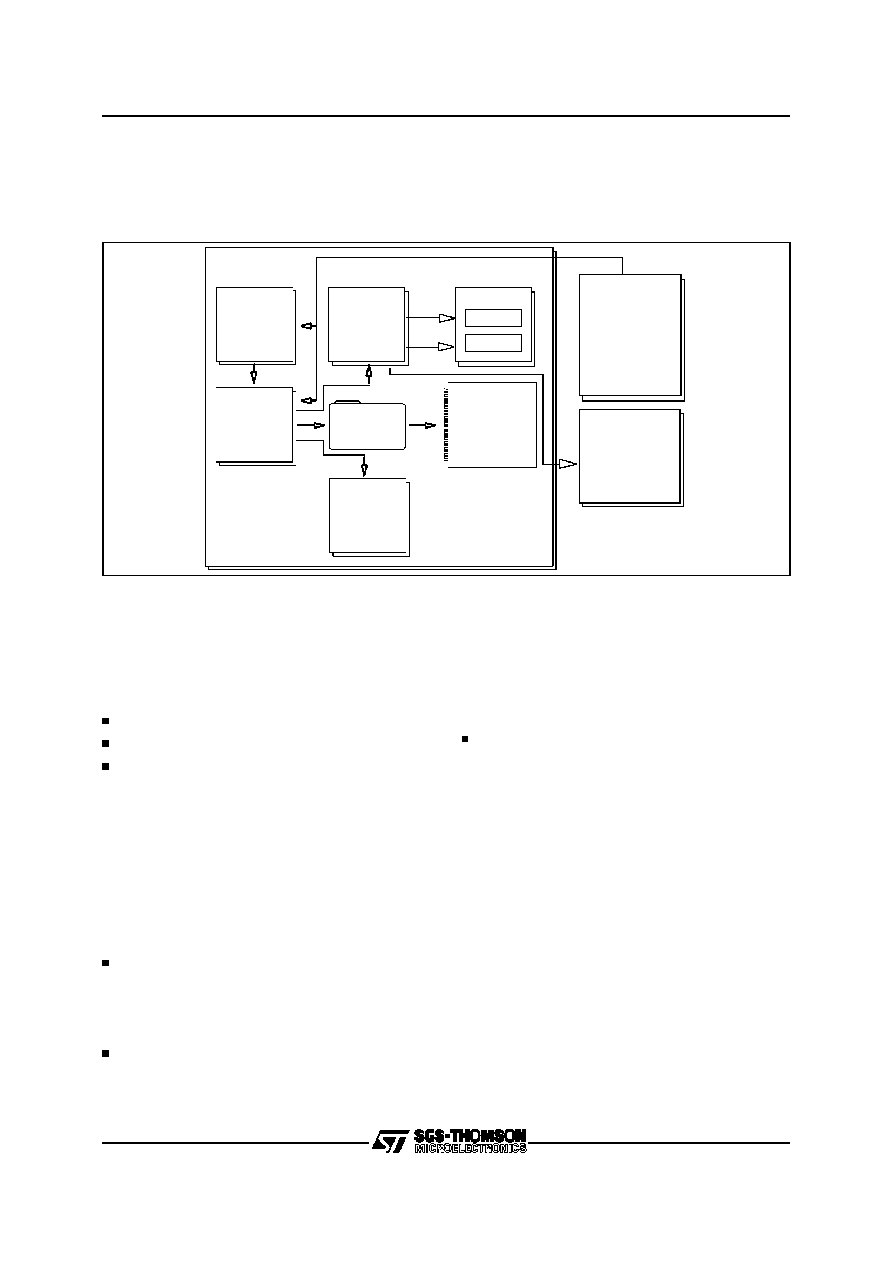
Figure 4. Block Diagram
6/19
W.A.R.P.1.1
provided by W.A.R.P. by means of A0-A9 and
EPA0-EPA2 output pins.
Data must be loaded 8 bit a time in the data bus
and can be read from an external non volatile
memory or loaded by an host processor.
ON-LINE MODE
In On-line mode W.A.R.P. is enabled to elaborate
input values and calculate outputs according to the
fuzzy rules stored into the microprogram. W.A.R.P.
reads the input values one a time in the input data
bus when all the inputs are given, a NP signal is
pulled high to indicate that the computation is start-
ing. The computational phase is divided in two main
parts. During the first one the input values are read
and the corresponding ALPHA values (activation
levels) are extracted from the internal memories. In
the second part the computation of the fuzzy rules
and the defuzzification are implemented.
The block diagram shown in figure 3 describes the
structure of W.A.R.P..
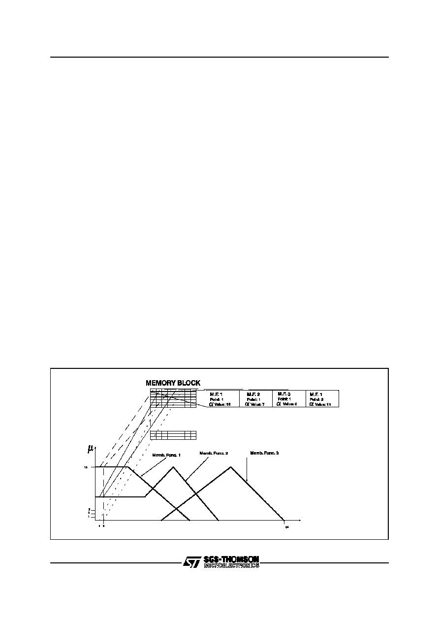
Antecedent Memory. It is formed by 4 benchs
each one containing one to four fuzzy sets bonded
to the input variables.
Consequent Memory. It is formed by one bench
where the fuzzy sets bondedto the output variables
are stored .
Program Memory. It is formed by a single bench.
Each line contains an operating code to execute
the computation of a rule. This code selects the
antecedentweights (ALPHA) involved in a rule, and
connects them by the programmed connective op-
erators (AND,OR).
Input Router. This internal block performs the
input data routing. Data are read one byte a time
from the input data bus, stored in 4 different buffers
and, thanks to a pipeline process, sent together to
4 indipendent modules to be processed in parallel
according to the chosen set-up configuration. Input
data resolution is decided by the user (MAX 128
points) according to the available configurations,
as shown in table 5.
The cycle starts when a positive pulse is applied at
FIN for a time no lower than an entire clock period
and continues until a new FIN (after NP low) or a
PRST signal is given.
Fuzzifier. This block generates the addresses of
the antecedentmemories where the ALPHA values
for each sampled input value are stored. It reads
the first four input values and calculates the corre-
sponding antecedent memories addresses. After-
wards it reads other four inputs values and
simultaneously sends, thanks to a pipeline proc-
ess, the previous four ALPHA values into internal
registers. These ALPHAvalues are then sent to the
Inference Unit. W.A.R.P. stores all ALPHA values
comprising a term set, which is formed by the MFs
connected to the IF-part of a rule, in successive
memory locations of the same memory word (see
figure 4). The vectors characterizing the MFs of a
term set are stored so that the ALPHAs of different
MFs corresponding to the same universe of dis-
course point (for the same input) are stored se-
quentially. So W.A.R.P. retrieves all the alpha
values of a term set using the crisp input value to
calculate the memory word address in the used
fuzzy memory device.The Fuzzifier Unit is driven
Figure 5. Antecedent Memory Organization
7/19
W.A.R.P.1.1
by the configuration in accordance with the antece-
dent part of the fuzzy rules. The duration of the
fuzzification process depends from the chosen
configuration and the input number.
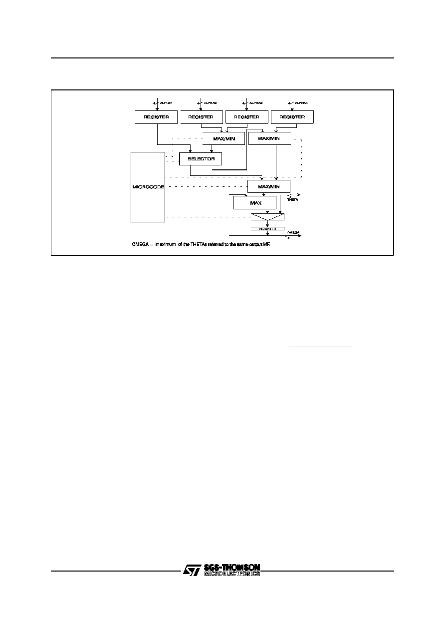
Inference Unit. Thanks to the Theta Operator, the
Inference Unit generates the THETA weights which
are used to manipulate the consequent MFs.
This is a calculation of the maximum and/or mini-
mum performed on ALPHA values according to the
logical connectives of fuzzy rules. It is possible to
utilize the AND/OR connectives and to directly ex-
ploit ALPHA weights or the negated values. The
number of THETA weights depends on the number
of rules.
The rules can have at maximum four ALPHA
weights (however they are connected). Two or
more rules can be only joined with the OR connec-
tive.
Inference Unit structure is shown in figure 5.
Defuzzifier. It generates the output crisp values
implementing the consequent part of the rules ac-
cording to MAX-DOT method.
In this method consequent MFs are multiplied by a
weight value
(OMEGA
)
, which is calculated on
the basis of antecedent MFs and logical operators.
All the terms needed to evaluate sums in numerator
and denominator of center of gravity equation (see
formula) are stored during the off-line phase.
The processing of fuzzy rules produces, for each
output variable, a resulting membership function.
Each MF related to the processed output variable
is firstly modified by a rule weight in accordance to
MAX-DOT method.
Output value (X) is deduced from the centroids (x
i
)
and the modified MFs (
i
*A
i
) by using the formula:
X
=
1
n
i
A
i
x
i
1
n
i
A
i
n = number of MFs defined for the Output Variable
A
i
= MF
i
Area
x
i
=absciss of the MF
i
centroid
i
=membership degree of the output MF
i
.
To represent a membership function related with
the THEN-part of a rule W.A.R.P. uses a single
memory bench. For each consequent MF each
memory word contains both the area multiplied with
the barycentre and the area itself. This area is
related to the first truth level (there are 16 truth
levels (4 bit), so a multiplication with the calculated
THETA must be performed on-line.
Two parallel blocks calculate the numerator and
denominator values to implement the centroids
formula. A final division block calculates the output
values (see figure 6).
Figure 6. Inference Unit Structure
8/19
W.A.R.P.1.1

Figure 7. Defuzzifier Structure
Symbol
Parameter
Min
Typ
Max
Unit
V
IL
Low Level Input Voltage
0.8
V
V
IH
High Level Input Voltage
2.0
V
V
OL
Low Level Output Voltage
0.2
0.4
V
V
OH
High Level Output Voltage
2.4
3.4
V
I
IL
Low Level Input Current
V
I
=V
SS
+1
µ
A
I
IH
High Level Input Current
V
I
=V
DD
-1
µ
Table 6. DC Characteristics
ELECTRICAL SPECIFICATIONS
DC PARAMETRICS Across Temperature Range (T=0 to +70
∞
C unless otherwise specified) -
TTL INTERFACE
0.4V
2.4V
0.8V
2V
0.4V
2.4V
Input
Output
9/19
W.A.R.P.1.1
Symbol
Parameters
Test Conditions
CK=20MHz
Min
Max
CK=40MHz
Min
Max
Unit
t
CP
Clock Period
50
25
ns
t
CLH
Clock High
20
30 10
15
ns
t
CLL
Clock Low
20
30 10
15
ns
t
CR
Clock Rise
0.8V to 2V
4
4
ns
t
CF
Clock Fall
2V to 0V
4
4
ns
t
SET
Setup
12
12
ns
t
HLD
Hold
15
15
ns
Table 7. AC Characteristics
DC PARAMETRICS
DC PARAMETRICS Across Temperature Range (T=0 to +70
∞
C unless otherwise specified
TTL INTERFACE
t
CLL
t
CLH
50 %
5 0%
50 %
t
SE T
t
HLD
Clock
Dat a
C P
t
10/19
W.A.R.P.1.1

W.A.R.P. TIMING TABLES
Off-line Phase Timing (Internal RAMs Loading with Charge Mode "0")
O F L
I0 - I6
D ATA 0
D ATA n
D ATA 1
M C L K
F IN
N P
E P
F IN d e t e c t io n
D AT A 0 a c q u i s iti o n
D AT A 1 a c q u i s iti o n
D ATA n a c q u is it io n
T
A C Q
T
A C Q =
2 0 0 n s fo r a c o n fig u r a tio n w ith 1 6 in p u t s , 8 o u tp u t s , 2 8 r u le s
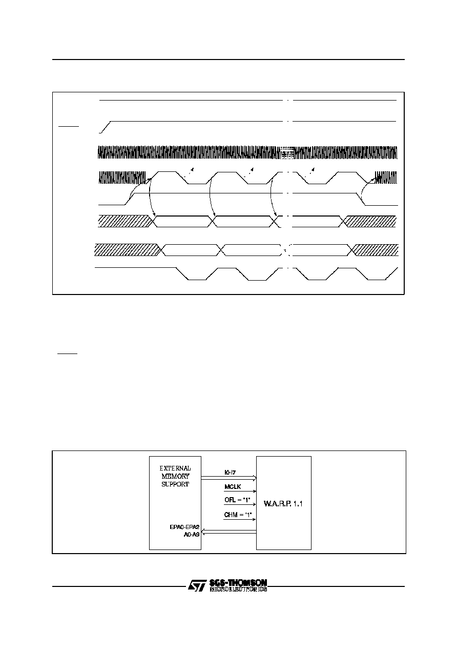
Timing Table Description: OFF-LINE phase (CHM "0")
- CHM [INPUT] low will enable the 'manual downloading' by specifying the address and data to be loaded
into W.A.R.P..
- MCLK [INPUT] must be connected with the external synchronization signal.
- PRST [INPUT] must be set high to enable the device.
- OFL [INPUT] must be set high to enable the configurationloading phase into the internal RAMs of W.A.R.P..
- The input to be written into the internal memories at the address specified in A0-A9 must be put into I0-I7
bus .
- SYNC [OUTPUT] will be provided to synchronize input data (I0-I7,A0-A9) coming from an external
database. SYNC frequency is MCLK/32 with a phase delay of t
CSP
ns . W.A.R.P. stores the data present
on input buses at the rising edge of MCLK, returns a SYNC pulse after t
CSP
ns indicating that is waiting for
new data and address that must be given within next 31MCLK pulses. Afterwards W.A.R.P. stores the data
on input buses and restores a new SYNC pulse.
W.A.R.P. stores the data situated in I0-I7 and the addresses A0-A9 into its internal registers.
Figure 8.
Block Diagram for W.A.R.P. downloading (CHM "0")
11/19
W.A.R.P.1.1
Off-line Phase Timing (Internal RAMs Loading with Charge Mode "1")
D C LK
O F L
I0 -I7
E PA 0 -E PA2 +
A 0 -A 9
AD D R E S S 0
AD D R E S S 1
AD D R E S S n
M C LK
D ATA 0
D ATA n
DATA 1
W .A.R .P. st o re s D ATA0
W .A.R . P. st o re s D ATA1
W .A.R .P. st o re s D ATAn
P R S T
C H M
S YN C
Timing Table Description: OFF-LINE phase (CHM "1")
- CHM [INPUT] high will enable the 'automatic downloading', specifying the address of the non-volatile
memory where are data to be loaded into W.A.R.P.. Internal memory addresses are automatically
generated.
- MCLK [INPUT] must be connected with the external synchronization signal.
- PRST [INPUT] must be set high to enable the device.
- OFL [INPUT] must be set high to enable the loading phase of data into the internal RAMs of W.A.R.P..
- SYNC [OUTPUT] will be provided to synchronize input data (I0-I7) coming from the external database.
SYNC frequency is MCLK/32.
- DCLK [INTERNAL] sets the working frequencyaccordingto the OFL control signal. It drives the addressing
of data coming from the external memory support by the I0-I7 input bus. The external memory support must
return the data (addressed by EPA0-EPA2+A0-A9 [OUTPUT]) into I0-I7 in a period of time no longer than
half a period of DCLK. DCLK frequency is MCLK/32.
Figure 9.
Block Diagram for W.A.R.P. downloading (CHM "1")
12/19
W.A.R.P.1.1
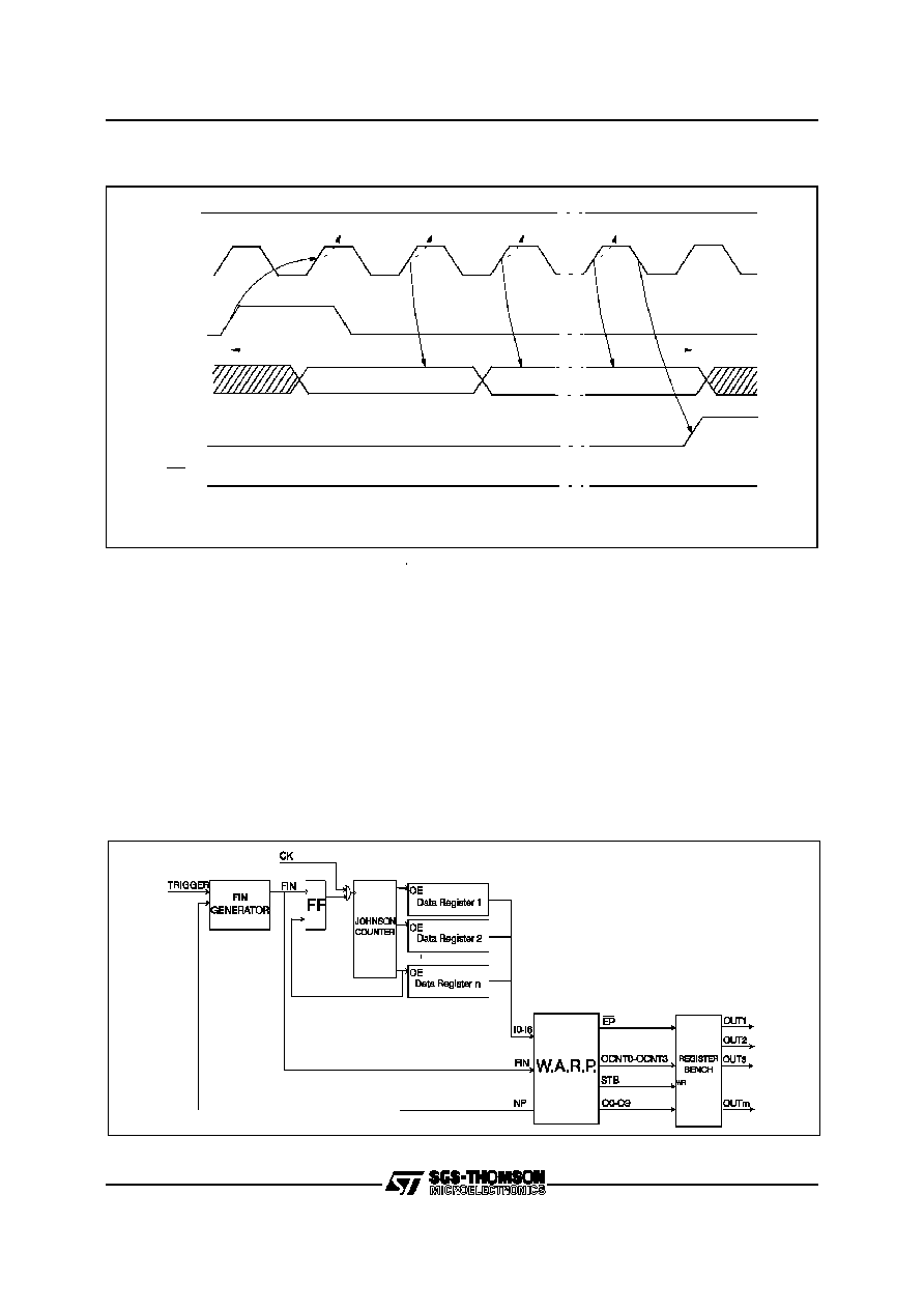
On-line Phase Timing (Acquisition and Elaboration) Working Frequency 40MHz
OFL
I0-I6
DATA0
DATAn
DATA1
MCLK
FIN
NP
EP
FIN de tection
DATA0 acq uisition
DATA1 a cquisition
DATAn acquisition
T
ACQ
T
ACQ =
2 00 ns for a configuration with 16 input s, 8 outputs , 2 8 rules
Timing Table Description: ON-LINE phase
1
st
step: Acquisition
- MCLK [INPUT] must be connectedwith the external synchronization signal.
- OFL [INPUT] must be set low to enable the acquisition/elaboration phase of W.A.R.P..
- FIN [INPUT] must be set high for at least 1clock period to start the acquisition phase. OFL must already
be low since at least 4 clock periods before providing a FIN pulse. FIN duration must be in the range
[1clock,2clock periods]. FIN pulse mustn't coincide with NP transitions.
- NP [OUTPUT] will remain low during the acquisition phase.
- The input data must be sent to I0-I6 after OFL has been set low and FIN has been set high. Data situated
in I0-I6 are stored into its internal registers at each next rising edge of the MCLK.
- After the current inputs have been acquired, the NP [OUTPUT] high signal informs that the elaboration
phase can start. This information is provided thanks to the configuration stored in the program memory.
Figure 10. Input/Output Connection Block Diagram
13/19
W.A.R.P.1.1
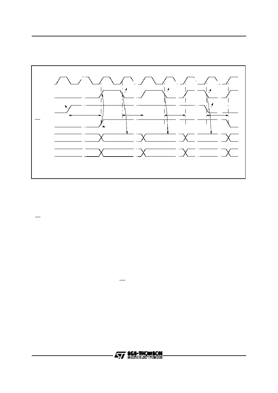
On-line Phase Timing (Output Generation) Working Frequency 40MHz
O0-O9
MCLK
NP
EP
e nd of
c o mputation
OCNT0-3
S TB
s t art of
c om putation
d ata output
st orag e
d ata output
st orag e
la st output da ta
OUT NUM n -1
la st output number
NEW DATA
ACQUISITION
DATA OUT 1
d ata ou tput
st ora g e
T
c omp=
600 ns (first proce s s , pipeline empty), 310 ns (next proce s s e s ) for a configuration with 16 inputs, 8 outputs, 28 rules
Ela ps ed time from the first data acquisition to the first output: 810 ns for the first cycle , 525ns for the other ones
.
T
COM P
OUT NUM 1
OUT NUM 2
DATA OUT n-1
DATA OUT 2
T
COM P
T
COM P
T
COM P
Timing Table Description: ON-LINE phase
2
nd
step:Elaboration
- MCLK [INPUT] must be connectedwith the external synchronization signal.
- OFL [INPUT] must remain low during this phase.
- NP [OUTPUT] remains high during this phase.
- EP [OUTPUT] is set high during this phase.
- STB [OUTPUT] is set high for a clock period every time an output value has been calculated. It informs
that it is possible to utilize the output which is situated in the output bus (O0-O9). The STB pulse starts at
the rising edge of the MCLK and stops at the next rising edge of the MCLK. At the falling edge of the STB
the data situated on the O0-O9 bus can be stored.
- The current output on the O0-O9 [OUTPUT] bus is provided exactly when the STB signal rises and it
does not change until a new STB signal occurs.
- The output identifier on the OCNT0-OCNT3 [OUTPUT] bus is provided exactly when the STB signal rises
and it does not change until a new STB signal occurs.
- NP [OUTPUT] is set low when the penultimate STROBE is disabled allowing a new acquisition phase to
start while W.A.R.P. is still elaborating the last output.
- When the last output has been provided, EP will be automatically set low.
14/19
W.A.R.P.1.1
PROGRAMMING TOOL
FUZZYSTUDIO
TM
TM
1.0 - W.A.R.P. Software Development Tool
SGS-THOMSON has developed some software
tools (see figure 11) to support the use of W.A.R.P.1
allowing easy configurating and loading of the
memories and functional simulations. It is fully com-
patible with the W.A.R.P. board.
It has been designed in order to be used with the
following hardware/software requirements:
80386 (or higher) processor
VGA / SVGA screen
Windows Version 3.0 or Higher
The constituting blocks are:
W.A.R.P.-SDT Editor:
it is a tool to define the fuzzy controller with a
User-Friendly Interface.
It is composed by:
≠ Variable Editor (to define the I/O variable)
≠ Membership Editor (to define the member-
ship function shape)
≠ Rule Editor (to define the base of knowledge)
W.A.R.P-SDT Compiler:
it generates the code to be loaded in W.A.R.P.
memories according to the data defined through
the editor. It also generates the data base for
Debugger, Exporter and Simulator.
W.A.R.P-SDT Debugger:
it allows the user to examine step-by-step the fuzzy
computation for a defined application. It also allows
to check the results of the entire control process
by using a list of patterns stored into a file.
It allows to show:
≠ Alpha values
≠ Theta values
≠ Defuzzification partial values
≠ Output values
W.A.R.P.-SDT Exporter:
it generates files to be imported in different environ-
ments in order to develop W.A.R.P. based simula-
tions exploiting user-developed models.
It addresses the following environments:
Standard C: the exporter generates a C function
that can be recalled by an user program
Matlab: the exporter generates a '.M' file that can
be used to perform simulations in Matlab environ-
ments
W.A.R.P.-SDT Simulator:
it allows to:
≠ define models of the controlled system in
terms of differential equations
≠ define the external inputs and set points
≠ resolve the differential equations by using
Runge-Kutta algorithm
≠ functionally simulate W.A.R.P.
≠ show the simulation results in graphic
charts.
ANCILLARY,
HIGH LEVE L
RULE
E XTRAC TOR
&
O PTIMIZER
FUZZYSTUDIO
S IMULATOR
P ro p rie ta ry
EDITOR
C OMP ILER
FUZZYSTUDIO
AP PLICATION
DEVELOPMENT
BOARD
DEB UGGER
INTEL HX
FILE
RS232
SUPPORT TOOLS
SU PP ORT TOO LS
BASIC TOOLS
MATLAB
C mode l
EMULATOR
EXPORTER
FUZZYSTUDIO
MODELER
FUZZYSTUDIO
W.A.R.P.-SDT
TM
TM
TM
TM
Figure 11. W.A.R.P. Software Development Tools
15/19
W.A.R.P.1.1
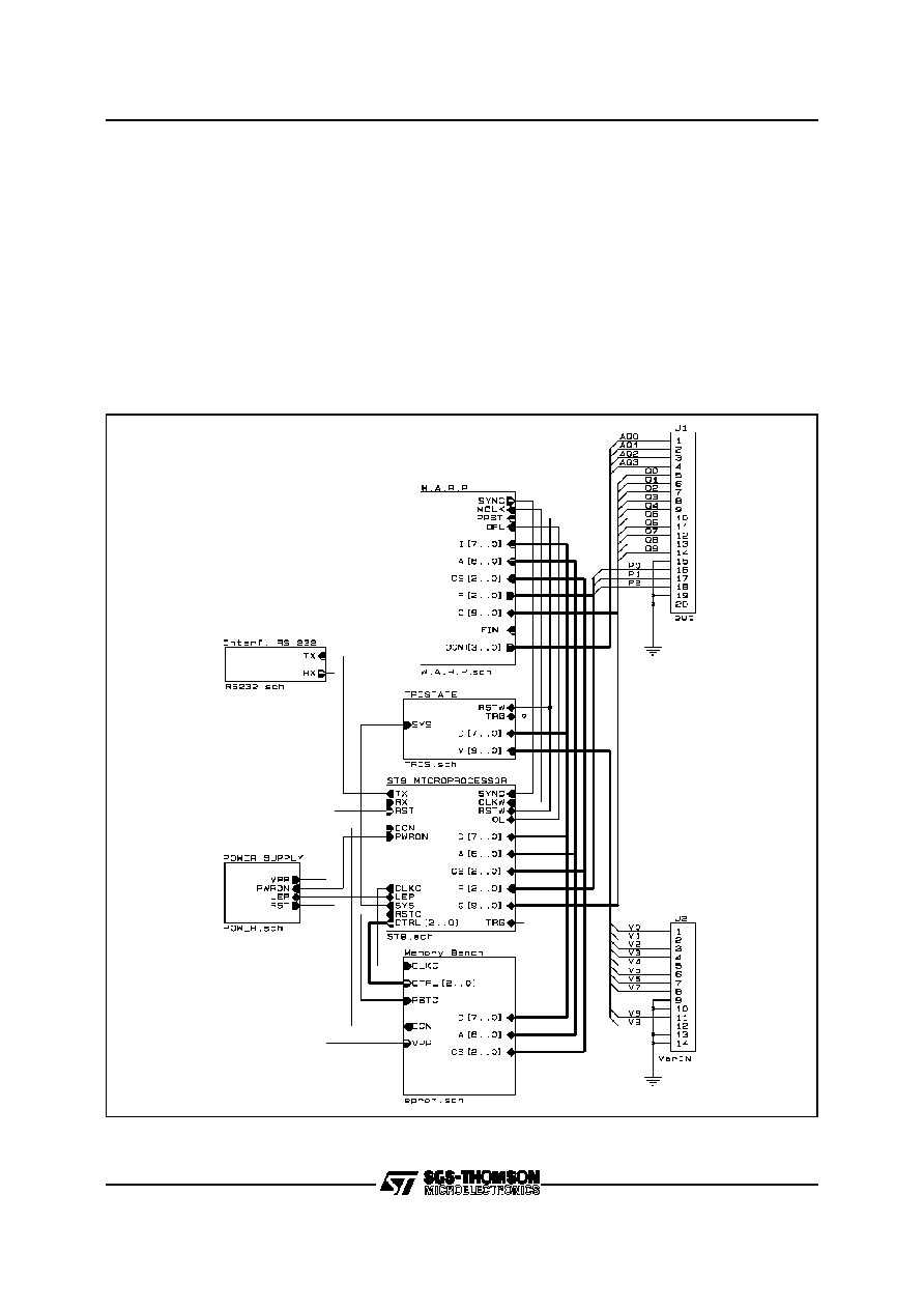
W.A.R.P. Application Development Board
The board has been designed to be connected to
the RS232 port of an IBM PC 386 (or higher), but
it can also work stand alone. Inputs and outputs are
provided at TTL compatible level. The board allows
the user to charge the rules and the membership
functions (see W.A.R.P.-SDT User Manual) into the
W.A.R.P. memories.
It can manage up to 16 inputs and 16 outputs.
The clock generatorfrequency on board is 24MHz.
An automatic trigger is used to synchronize
W.A.R.P. with the external environment (working
connected with a PC).
When the board is used as a stand alone device all
the fuzzy data (membership functions and rules)
are stored in EPROMs. The board allows the stand-
alone/PC working to be selected by setting a switch
(see W.A.R.P.-SDT User Manual). A block diagram
of the board is described in figure 12.
Figure 12. Board Block Diagram
16/15
16/19
W.A.R.P.1.1
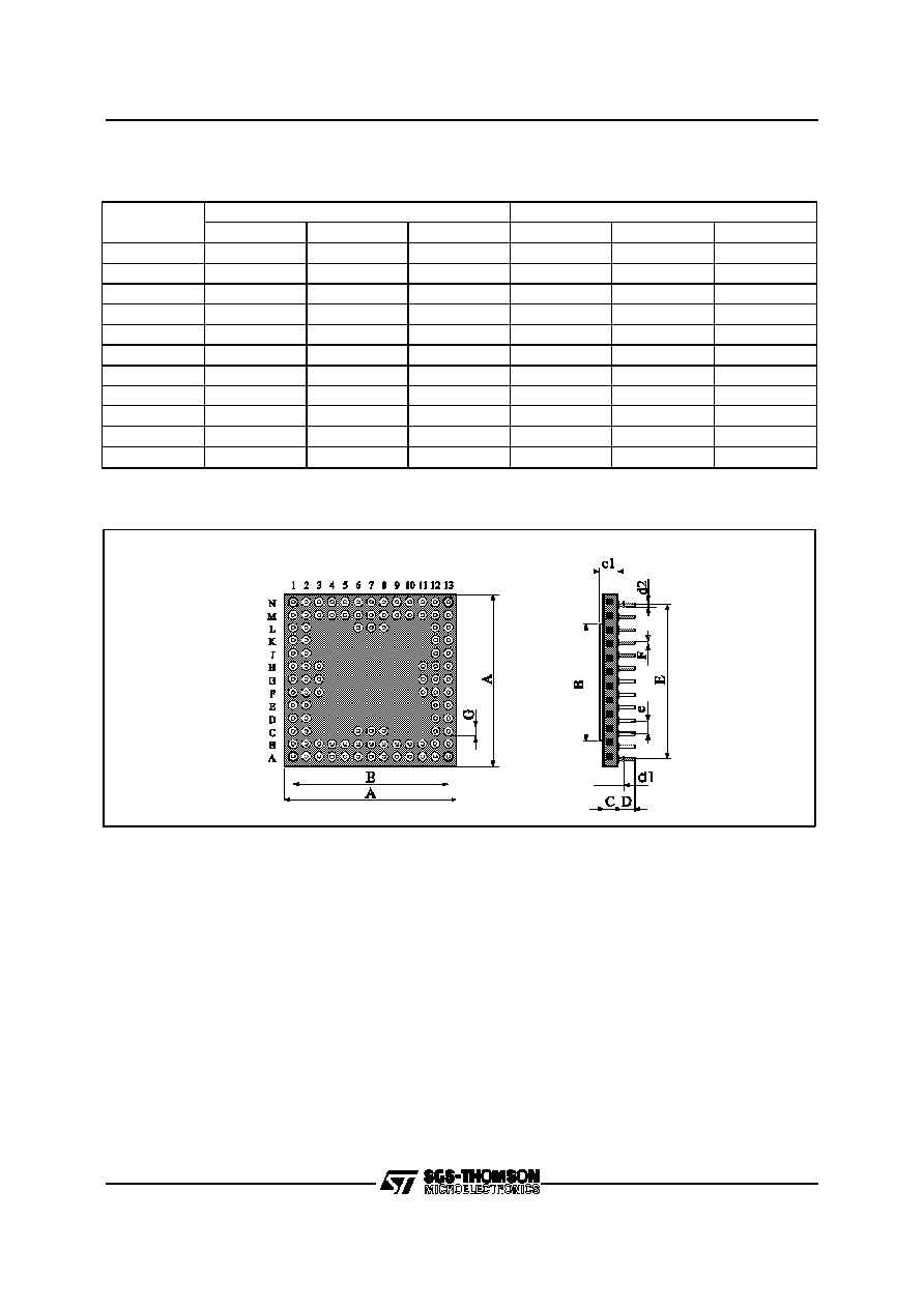
PACKAGE DIMENSIONS
Dim.
mm
inch
Min.
Typ.
Max.
Min.
Typ.
Max.
A
4.20
5.08
0.16
0.19
A1
0.56
0.02
A3
2.54
0.10
B
0.38
0.01
B1
1.14
0.003
D
30.10
30.35
1.18
1.19
D1
29.20
29.41
1.14
1.15
D3
27.69
28.70
1.11
1.13
E
30.10
30.35
1.18
1.19
E1
29.20
29.41
1.14
1.15
E3
27.69
28.70
1.11
1.13
e
1.27
0.05
D
30.10
30.35
1.18
1.19
D1
29.20
29.41
1.14
1.15
D3
27.69
28.70
1.11
1.13
F
0.50
0.020
G
1.78
0.070
Pin 1
VR01534
D3
D1
D
K1
E
E3
E1
B
h
h
B1
e
A1
A3
A
L
NE
ND
Number of Pins
Nu
m
b
er
of
P
i
ns
Figure 13. W.A.R.P. 84 Pin PLCC84 Plastic Package
17/19
W.A.R.P.1.1
PACKAGE DIMENSIONS
Dim.
mm
inch
Min.
Typ.
Max.
Min.
Typ.
Max.
A
33.58
1.332
B
17.78
0.700
C
2.24
0.088
c1
2.54
0.100
D
4.70
0.185
d1
1.40
0.055
d2
1.68
0.065
E
30.78
1.212
e
2.54
0.100
F
0.50
0.020
G
1.78
0.070
Figure 14. W.A.R.P. 100 Pin CPGA100 Ceramic Package
18/19
W.A.R.P.1.1

Information furnished is believed to be accurate and reliable. However, SGS-THOMSON Microelectronics assumes no responsibility for the
consequences of use of such information nor for any infringement of patents or other rights of third parties which may result from its use. No
license is granted by implication or otherwise under any patent or patent rights of SGS-THOMSON Microelectronics. Specification mentioned
in this publication are subject to change without notice. This publication supersedes and replaces all information previously supplied.
SGS-THOMSON Microelectronics products are not authorized for use as critical components in life support devices or systems without express
written approval of SGS-THOMSON Microelectronics.
©
1996 SGS-THOMSON Microelectronics ≠ Printed in Italy ≠ All Rights Reserved
FUZZYSTUDI O
TM
is a trademark of SGS-THOMSON Microelectronics
MS-DOS
Æ
, Microsoft
Æ
and Microsoft Windows
Æ
are registered trademarks of Microsoft Corporation.
MATLAB
Æ
is a registered trademark of Mathworks Inc.
SGS-THOMSON Microelectronics GROUP OF COMPANIES
Australia - Brazil - Canada - China - France - Germany - Hong Kong - Italy - Japan - Korea - Malaysia - Malta - Morocco - The Netherlands -
Singapore - Spain - Sweden - Switzerland - Taiwan - Thailand - United Kingdom - U.S.A.
Part Number
Maximum Frequency
Supply Voltage
Temperature Range
Package
STFLWARP11/PG
40 MHz
5
±
5%
0
∞
C to 70
∞
C
CPGA100
STFLWARP11/PL
40 MHz
5
±
5%
0
∞
C to 70
∞
C
PLCC84
Table 8. Ordering Information
Type
Device
Development Tools
FUZZYST UDIO
TM
TM
ADB
FUZZYSTUDIO
TM
TM
SDT
STFLSTUDIO10/KIT
STFLWARP11/PG
STFLWARP11/PL
W.A.R.P. 1.X
W.A.R.P. 1.X programmer
EPROM programmer
RS-232 communication handler
Internal Clock
Variables and Rules Editor
W.A.R.P. Compiler/Debugger
Exporter for ANSI C and MATLAB
Æ
Order Code
Description
Supported Target
Functionalities
System Requirement
STFLAFM10/SW
WTA-FAM for Building Rules
BACK-FAM for Building MFs
STFLWARP11/PG
STFLWARP11/PL
STFLWARP20/PL
ANSI C
MATLAB
Æ
Rules Minimizer
Step-by-Step Simulation
Simulation from File
Local Tuning
MS-DOS 3.1or higher
Windows 3.0 or later
486, PENTIUM compatible
8 MB RAM
Functionsin dedicated memories in order to reduce
the computational time. Therefore a great amount
of W.A.R.P. processing is based on a look-up table
approach rather than on on-line calculation.
Those Membership Functions (MFs), each one
portrayed by a configurable resolution of 2
6
or 2
7
elements, are stored in four internal RAMs (1Kbyte
each). The consequent MFs, due to the different
modelling, are loaded in a single RAM by storing
for each MF its area and its barycentre. This is due
to the adoptionof the Center of Gravity defuzzifica-
tion method.
The downloading phase allows the setting of the
device, in terms of I/O number, universes of dis-
course and MF shapes. During this phase W.A.R.P.
prepares its internal memories for the on-line
elaboration phase and loads the microcode in its
program memory. This microcode, which drives the
on-line phase, is generated by the Compiler (see
W.A.R.P.-SDT User Manual) according to the
adopted configuration. The possible configurations
are shown in table 1.
During the on-line phase (up to 40MHz working
frequency), W.A.R.P. processes the input data and
produces its outputs according to the configuration
loaded in the downloading phase.
W.A.R.P. is conceived to work together with tradi-
tional microcontrollers which shall perform normal
control tasks while W.A.R.P. will be indipendently
responsible for all the fuzzy related computing.
W.A.R.P. is manufactured using the high perform-
ance, reliable HCMOS4T (O.7
µ
m) SGS-THOMSON
Microelectronics process.
19/19
W.A.R.P.1.1