PRODUCT SELECTION GUIDE
PARAMETER
27C010L-90
27C010L-12
27C010L-15
27C010L-17
27C010L-20
Address Access Time (Max)
90 ns
120 ns
150 ns
170 ns
200 ns
Chip Select Time (Max)
90 ns
120 ns
150 ns
170 ns
200 ns
Output Enable Time (Max)
35 ns
35 ns
40 ns
40 ns
40 ns
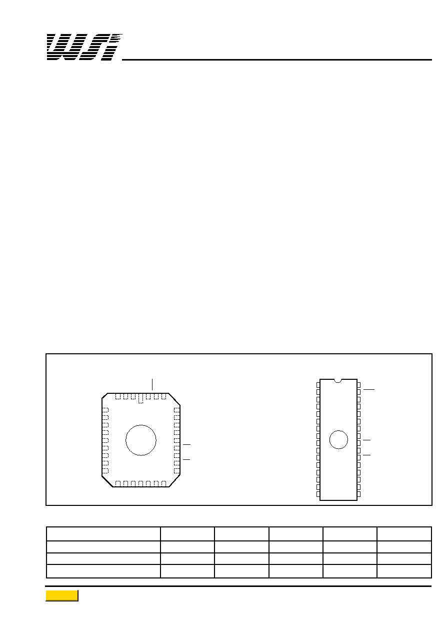
WS27C010L
TOP VIEW
Chip Carrier
CERDIP
PIN CONFIGURATION
4-25
Military 128K x 8 CMOS EPROM
KEY FEATURES
∑
High Performance CMOS
∑
DESC SMD No. 5962-89614
-- 90 ns Access Time
∑
Compatible with JEDEC 27010 and
∑
Fast Programming
27C010 EPROMs
∑
EPI Processing
∑
JEDEC Standard Pin Configuration
-- Latch-Up Immunity to 200 mA
-- 32 Pin CERDIP Package
-- ESD Protection Exceeds 2000 Volts
-- 32 Pin Leadless Chip Carrier (CLLCC)
GENERAL DESCRIPTION
The WS27C010L is a performance oriented 1 Meg UV Erasable Electrically Programmable Read Only Memory
organized as 128K words x 8 bits/word. It is manufactured using an advanced CMOS technology which enables it to
operate at data access times as fast as 120 nsecs. The memory was designed utilizing WSI's patented self-aligned
split gate EPROM cell, resulting in a low power device with a very cost effective die size.
The WS27C010L 1 Meg EPROM provides extensive code store capacity for microprocessor, DSP, and
microcontroller-based systems. Its 120 nsec access time over the full Military temperature range provides the
potential of no-wait state operation. And where this parameter is important, the WS27C010L provides the user with
a very fast 35 nsec T
OE
output enable time.
The WS27C010L is offered in both a 32 pin 600 mil CERDIP, and a 32 pad Ceramic Leadless Chip Carrier
(CLLCC) for surface mount applications. Its standard JEDEC EPROM pinouts provide for automatic upgrade
density paths for existing 128K and 256K EPROM users.
A
14
A
13
A
8
A
9
A
11
OE
A
10
CE
O
7
A
7
A
6
A
5
A
4
A
3
A
2
A
1
A
0
O
0
A
12
A
15
A
16
V
PP
V
CC
PGM
NC
O
1
O
2
O
3
O
4
O
5
O
6
1
4 3
2
32 31 30
29
28
27
26
25
24
23
22
21
5
6
7
8
9
10
11
12
13
14 15 16 17 18 19 20
GND
V
CC
PGM
NC
A14
A13
A8
A9
A11
OE
A10
CE
O
7
O
6
O
5
O
4
O
3
V
PP
A
16
A
15
A
12
A
7
A
6
A
5
A
4
A
3
A
2
A
1
A
0
O
0
O
1
O
2
GND
1
2
3
4
5
6
7
8
9
10
11
12
13
14
15
16
32
31
30
29
28
27
26
25
24
23
22
21
20
19
18
17
Return to Main Menu
AC READ CHARACTERISTICS
Over Operating Range with V
PP
= V
CC
.
SYMBOL
PARAMETER
-90
-12
-15
-17
-20
UNITS
MIN
MAX
MIN
MAX
MIN
MAX
MIN
MAX
MIN
MAX
t
ACC
Address to Output Delay
90
120
150
170
200
t
CE
CE to Output Delay
90
120
150
170
200
t
OE
OE to Output Delay
35
35
40
40
40
t
DF
Output Disable to
Output Float (Note 3)
35
35
40
40
40
ns
Output Hold from
t
OH
Addresses, CE or OE,
0
0
0
0
0
Whichever Occurred
First (Note 3)
DC READ CHARACTERISTICS
Over Operating Range. (See Above)
SYMBOL
PARAMETER
TEST CONDITIONS
MIN
MAX
UNITS
V
IL
Input Low Voltage
≠0.5
0.8
V
V
IH
Input High Voltage
2.0
V
CC
+ 1
V
V
OL
Output Low Voltage
I
OL
= 2.1 mA
0.4
V
V
OH
Output High Voltage
I
OH
= ≠400 µA
3.5
V
I
SB1
V
CC
Standby Current (CMOS) CE = V
CC
± 0.3 V (Note 2)
100
µA
I
SB2
V
CC
Standby Current
CE = V
IH
1
mA
I
CC
V
CC
Active Current (TTL)
CE = OE = V
IL
F = 5 MHz
50
mA
(Note 1)
F = 8 MHz
60
mA
I
PP
V
PP
Supply Current
V
PP
= V
CC
100
µA
V
PP
V
PP
Read Voltage
V
CC
≠0.4
V
CC
V
I
LI
Input Leakage Current
V
IN
= 5.5 V or Gnd
≠10
10
µA
I
LO
Output Leakage Current
V
OUT
= 5.5 V or Gnd
≠10
10
µA
WS27C010L
4-26
OPERATING RANGE
RANGE
TEMPERATURE
V
CC
Military
≠55∞C to +125∞C
+5V ± 10%
ABSOLUTE MAXIMUM RATINGS*
Storage Temperature............................≠65∞ to + 150∞C
Voltage on any Pin with
Respect to Ground ....................................≠0.6V to +7V
V
PP
with Respect to Ground...................≠0.6V to + 14V
V
CC
Supply Voltage with
Respect to Ground ....................................≠0.6V to +7V
ESD Protection ..................................................
>
2000V
NOTES: 1. The supply current is the sum of I
CC
and I
PP
. The maximum current value is with Outputs O
0
to O
7
unloaded.
2. CMOS inputs: V
IL
= GND ± 0.3V, V
IH
= V
CC
± 0.3 V.
*
NOTICE:
Stresses above those listed under "Absolute Maximum
Ratings" may cause permanent damage to the device.
This is a stress rating only and functional operation of
the device at these or any other conditions above
those indicated in the operational sections of this
specification is not implied. Exposure to absolute
maximum rating conditions for extended periods of
time may affect device reliability.
NOTE:
3. This parameter is only sampled and is not 100% tested. Output Float is defined as the point where data is no longer driven ≠ see timing
diagram.

SYMBOL
PARAMETER
CONDITIONS
TYP
(6)
MAX
UNITS
C
IN
Input Capacitance
V
IN
= 0V
4
6
pF
C
OUT
Output Capacitance
V
OUT
= 0V
8
12
pF
C
VPP
V
PP
Capacitance
V
PP
= 0 V
18
25
pF
4-27
WS27C010L
AC READ TIMING DIAGRAM
t
ACC
t
OH
ADDRESS VALID
VALID OUTPUT
ADDRESSES
V
IH
V
IL
t
OE
t
DF
t
CE
CE
OE
V
IH
V
IH
V
IL
V
IH
V
IL
V
IL
HIGH Z
HIGH Z
(5)
(4)
(4)
OUTPUT
CAPACITANCE
(5)
T
A
= 25∞C, f = 1 MHz
100 pF
(INCLUDING SCOPE
AND JIG
CAPACITANCE)
820
2.01 V
D.U.T.
A.C. TESTING INPUT/OUTPUT WAVEFORM
TEST LOAD
(High Impedance Test Systems)
2.4
0.4
2.0
0.8
2.0
0.8
TEST
POINTS
NOTE: 7. Provide adequate decoupling capacitance as close as possible to this device to achieve the published A.C. and D.C. parameters.
A 0.1 microfarad capacitor in parallel with a 0.01 microfarad capacitor connected between V
CC
and ground is recommended.
Inadequate decoupling may result in access time degradation or other transient performance failures.
NOTES: 5. This parameter is only sampled and is not 100% tested.
6. Typical values are for T
A
= 25∞C and nominal supply voltages.
A.C. testing inputs are driven at 2.4 V for a logic "1" and 0.4 V
for a logic "0." Timing measurements are made at 2.0 V for a
logic "1" and 0.8 V for a logic "0".
NOTE:
4. OE may be delayed up to t
CE
≠ t
OE
after the falling edge of CE without impact on t
CE
.

PROGRAMMING INFORMATION
DC CHARACTERISTICS
(T
A
= 25 ± 5∞C, V
CC
= 6.25 ± 0.25 V, V
PP
= 12.75 ± 0.25 V. See Notes 8, 9 and 10)
SYMBOLS
PARAMETER
MIN
MAX
UNITS
I
LI
Input Leakage Current (V
IN
= V
CC
or Gnd)
≠10
10
µA
I
PP
V
PP
Supply Current During
60
mA
Programming Pulse (CE = PGM = V
IL
)
I
CC
V
CC
Supply Current
50
mA
V
IL
Input Low Voltage
≠0.1
0.8
V
V
IH
Input High Voltage
2.0
V
CC
+ 0.3
V
V
OL
Output Low Voltage During Verify (I
OL
= 2.1 mA)
0.4
V
V
OH
Output High Voltage During Verify (I
OH
= ≠400 µA)
3.5
V
SYMBOLS
PARAMETER
MIN
TYP
MAX
UNITS
t
AS
Address Setup Time
2
µs
t
OES
Output Enable Setup Time
2
µs
t
OS
Data Setup Time
2
µs
t
AH
Address Hold Time
0
µs
t
OH
Data Hold Time
2
µs
t
DF
Chip Disable to Output Float Delay
0
55
ns
t
OE
Data Valid From Output Enable
55
ns
t
VS
/t
CES
V
PP
Setup Time/CE Setup Time
2
µs
t
PW
PGM Pulse Width
0.1
3
4
ms
WS27C010L
4-28
NOTES: 8. V
CC
must be applied either coincidentally or before V
PP
and removed either coincidentally or after V
PP
.
9. V
PP
must not be greater than 14 volts including overshoot. During CE = PGM = V
IL
, V
PP
must not be switched from 5 volts
to 12.75 volts or vice-versa.
10. During power up the PGM pin must be brought high (
V
IH
) either coincident with or before power is applied to V
PP
.
AC CHARACTERISTICS
(T
A
= 25 ± 5∞C, V
CC
= 6.25 ± 0.25 V, V
PP
= 12.75 ± 0.25 V)
PROGRAMMING WAVEFORM
ADDRESS STABLE
ADDRESSES
V
PP
V
PP
V
CC
V
IH
V
IL
CE
DATA
t
AS
t
PW
t
OS
t
OH
t
OE
t
AH
t
DF
t
VS
t
CES
t
OES
DATA OUT
DATA IN STABLE
OE
PGM
V
IH
V
IL
V
IH
V
IL
VALID
HIGH Z

ORDERING INFORMATION
OPERATING WSI
PART NUMBER
TEMPERATURE MANUFACTURING
RANGE
PROCEDURE
WS27C010L-12CMB
*
120
32 Pad CLLCC
C2
Military
MIL-STD-883C
WS27C010L-12DMB
*
120
32 Pin CERDIP, 0.6"
D4
Military
MIL-STD-883C
WS27C010L-15CMB
150
32 Pad CLLCC
C2
Military
MIL-STD-883C
WS27C010L-15DMB
150
32 Pin CERDIP, 0.6"
D4
Military
MIL-STD-883C
WS27C010L-17CMB
*
170
32 Pad CLLCC
C2
Military
MIL-STD-883C
WS27C010L-17DMB
*
170
32 Pin CERDIP, 0.6"
D4
Military
MIL-STD-883C
WS27C010L-20CMB
*
200
32 Pad CLLCC
C2
Military
MIL-STD-883C
WS27C010L-20DMB
*
200
32 Pin CERDIP, 0.6"
D4
Military
MIL-STD-883C
4-29
WS27C010L
NOTE: 14. The actual part marking will not include the initials "WS."
*SMD product. See page 4-2 for SMD number.
PROGRAMMING/ALGORITHMS/ERASURE/PROGRAMMERS
REFER TO
PAGE 5-1
The WS27C010L is programmed using Algorithm E shown on page 5-11.
(This product can also be programmed by using National Semiconductor's 27C010 Programming Algorithm.)
SPEED
PACKAGE
PACKAGE
(ns)
TYPE
DRAWING
MODE
PINS
CE
OE
PGM
A
9
A
0
V
PP
V
CC
OUTPUTS
Read
V
IL
V
IL
X
(11)
X
X
X
5.0 V
D
OUT
Output Disable
X
V
IH
X
X
X
X
5.0 V
High Z
Standby
V
IH
X
X
X
X
X
5.0 V
High Z
Programming
V
IL
V
IH
V
IL
X
X
V
PP
(12)
6.0 V
D
IN
Program Verify
V
IL
V
IL
V
IH
X
X
V
PP
(12)
6.0 V
D
OUT
Program Inhibit
V
IH
X
X
X
X
V
PP
(12)
5.0 V
High Z
Signature
Manufacturer
(13)
V
IL
V
IL
X
V
H
(12)
V
IL
X
5.0 V
23 H
Device
(13)
V
IL
V
IL
X
V
H
(12)
V
IH
X
5.0 V
C1 H
MODE SELECTION
The modes of operation of the WS27C010L are listed below. A single 5 V power supply is required in the read
mode. All inputs are TTL levels except for V
PP
and A
9
for device signature.
NOTES: 11. X can be V
IL
or V
IH
.
12. V
H
= V
PP
= 12.75 ± 0.25 V.
13. A
1
≠ A
8
, A
10
≠ A
16
= V
IL
.
Return to Main Menu