PRODUCT SELECTION GUIDE
PARAMETER
WS57C128FB-35
WS57C128FB-45
WS57C128FB-55
WS57C128FB-70
Address Access Time (Max)
35 ns
45 ns
55 ns
70 ns
Chip Select Time (Max)
35 ns
45 ns
55 ns
70 ns
Output Enable Time (Max)
20 ns
25 ns
25 ns
25 ns
WS57C128FB
3-7
HIGH SPEED 16K x 8 CMOS EPROM
KEY FEATURES
∑
Very Fast Access Time
∑
Standard EPROM Pinout
-- 35 ns
∑
DIP and Surface Mount Packaging
∑
Low Power Consumption
Available
∑
EPI Processing
-- Latch-up Immunity Up to 200 mA
GENERAL DESCRIPTION
The WS57C128FB is a High Performance 128K UV Erasable Electrically Programmable Read Only Memory. It is
manufactured with an advanced CMOS technology which enables it to operate at Bipolar speeds while consuming
only 90 mA.
Two major features of the WS57C128FB are its Low Power and High Speed. These features make it an ideal
solution for applications which require fast access times, low power, and non-volatility. Typical applications include
systems which do not utilize mass storage devices and/or are board space limited.
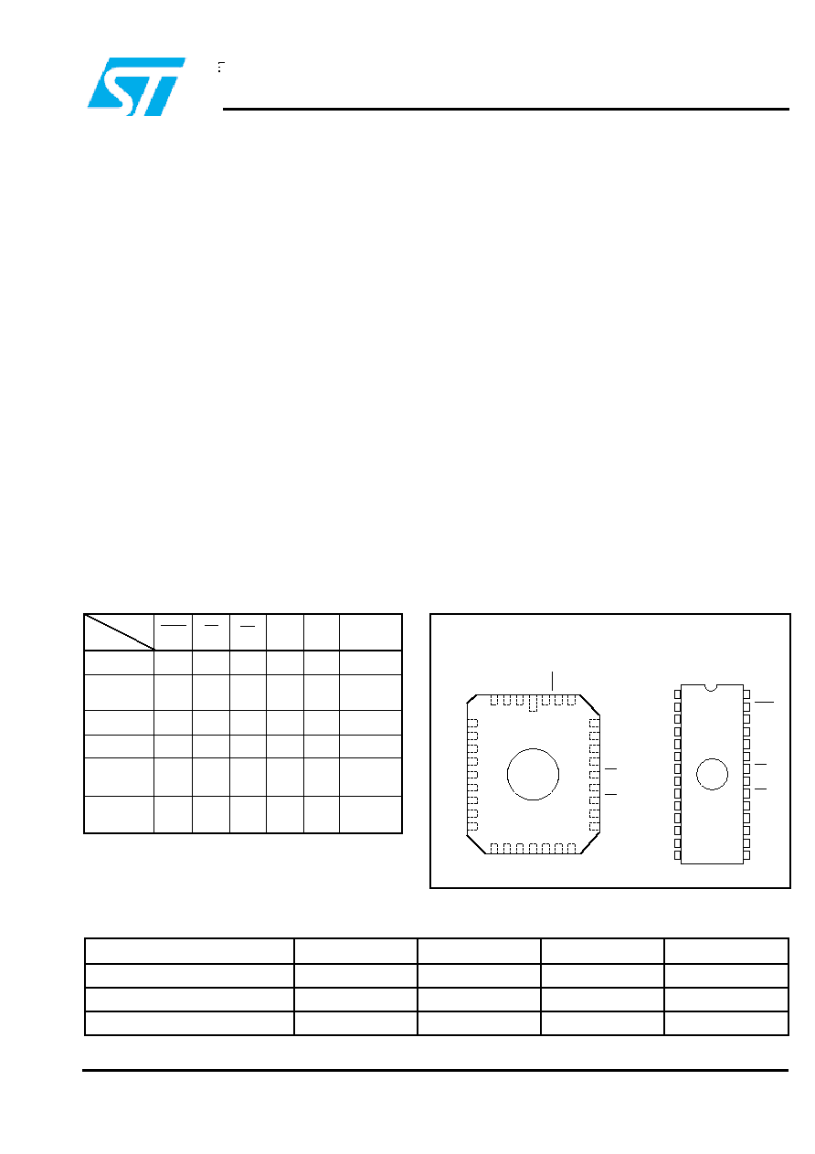
The WS57C128FB is configured in the standard EPROM pinout which provides an easy upgrade path for systems
which are currently using standard EPROMs. The EPROMs are available in both 600 Mil DIP packages, and both
J-leaded and leadless surface mount packages.
V
CC
PGM
A13
A8
A9
A11
OE
A10
CE
O
7
O
6
O
5
O
4
O
3
V
PP
A
12
A
7
A
6
A
5
A
4
A
3
A
2
A
1
A
0
O
0
O
1
O
2
GND
1
2
3
4
5
6
7
8
9
10
11
12
13
14
28
27
26
25
24
23
22
21
20
19
18
17
16
15
A
8
A
9
A
11
NC
OE
A
10
CE
O
7
O
6
A
6
A
5
A
4
A
3
A
2
A
1
A
0
NC
O
0
A
7
A
12
V
PP
NC
V
CC
PGM
A
13
O
1
O
2
NC
O
3
O
4
O
5
1
4 3
2
32 31 30
29
28
27
26
25
24
23
22
21
5
6
7
8
9
10
11
12
13
14 15 16 17 18 19 20
GND
TOP VIEW
Chip Carrier
CERDIP
PIN CONFIGURATION
PINS
PGM
CE
OE
VPP
VCC OUTPUTS
MODE
Read
X
VIL
VIL
VCC VCC
DOUT
Output
Disable
X
X
VIH
VCC VCC
High Z
Standby
X
VIH
X
VCC
VCC
High Z
Program
VIL
VIL
VIH
VPP
VCC
DIN
Program
Verify
VIH
VIL
VIL
VPP
VCC
DOUT
Program
Inhibit
X
VIH
X
VPP
VCC
High Z
X can be VIL or VIH.
MODE SELECTION
Return to Main Menu
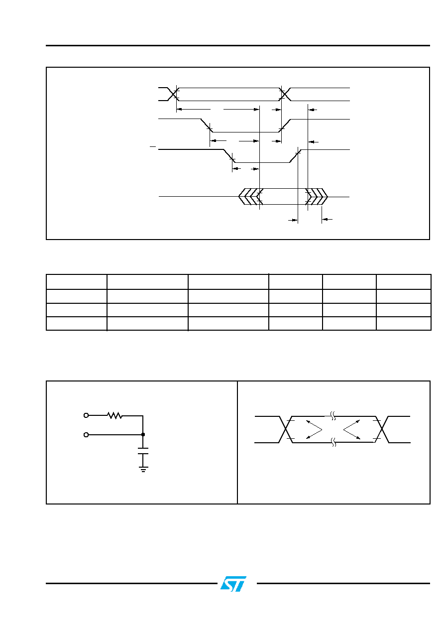
AC READ CHARACTERISTICS
Over Operating Range with V
PP
= V
CC
PARAMETER
SYMBOL
57C128FB-35 57C128FB-45 57C128FB-55
57C128FB-70
UNITS
MIN
MAX
MIN
MAX
MIN
MAX
MIN
MAX
Address to Output Delay
t
ACC
35
45
55
70
CE to Output Delay
t
CE
35
45
55
70
OE to Output Delay
t
OE
20
25
25
25
ns
Output Disable to
Output Float
t
DF
20
25
25
25
Address to Output Hold
t
OH
0
0
0
0
DC READ CHARACTERISTICS
Over Operating Range with V
PP
= V
CC
SYMBOL
PARAMETER
TEST CONDITIONS
MIN
MAX
UNITS
V
IL
Input Low Voltage
(Note 5)
≠ 0.1
0.8
V
V
IH
Input High Voltage
(Note 5)
2.0
V
CC
+ 0.3
V
V
OL
Output Low Voltage
I
OL
= 16 mA
0.4
V
V
OH
Output High Voltage
I
OH
= ≠ 4 mA
2.4
V
I
SB1
V
CC
Standby Current (CMOS)
(Notes 1 and 3)
500
µA
I
SB2
V
CC
Standby Current (TTL)
(Notes 2 and 3)
15
mA
(Notes 1 and 4)
Comm'l
30
mA
I
CC1
V
CC
Active Current (CMOS)
Outputs Not Loaded
Industrial
40
mA
Military
40
mA
(Notes 2 and 4)
Comm'l
50
mA
I
CC2
V
CC
Active Current (TTL)
Outputs Not Loaded
Industrial
60
mA
Military
60
mA
I
PP
V
PP
Supply Current
V
PP
= V
CC
100
µA
V
PP
V
PP
Read Voltage
V
CC
≠ 0.4
V
CC
V
I
LI
Input Leakage Current
V
IN
= 5.5V or Gnd
≠10
10
µA
I
LO
Output Leakage Current
V
OUT
= 5.5 V or Gnd
≠10
10
µA
OPERATING RANGE
RANGE
TEMPERATURE
V
CC
Commercial
0∞C to +70∞C
+5V ± 10%
Industrial
≠40∞C to +85∞C
+5V ± 10%
Military
≠55∞C to +125∞C
+5V ± 10%
WS57C128FB
3-8
ABSOLUTE MAXIMUM RATINGS*
Storage Temperature............................≠65∞ to + 150∞C
Voltage on any Pin with
Respect to Ground ....................................≠0.6V to +7V
V
PP
with Respect to Ground...................≠0.6V to + 13V
ESD Protection ..................................................
>
2000V
*
NOTICE:
Stresses above those listed under "Absolute Maximum
Ratings" may cause permanent damage to the device.
This is a stress rating only and functional operation of
the device at these or any other conditions above
those indicated in the operational sections of this
specification is not implied. Exposure to absolute
maximum rating conditions for extended periods of
time may affect device reliability.
NOTES:
1. CMOS inputs: GND ± 0.3V or V
CC
± 0.3V.
4. Add 4 mA/MHz for A.C. power component.
2. TTL inputs: V
IL
0.8V, V
IH
2.0V.
5. These are absolute voltages with respect to device ground pin and
3. Add 1 mA/MHz for A.C. power component.
include all overshoots due to system and/or tester noise.
Do not attempt to test these values without suitable equipment.
SYMBOL
PARAMETER
CONDITIONS
TYP
(7)
MAX
UNITS
C
IN
Input Capacitance
V
IN
= 0V
4
6
pF
C
OUT
Output Capacitance
V
OUT
= 0V
8
12
pF
C
VPP
V
PP
Capacitance
V
PP
= 0 V
18
25
pF
3-9
WS57C128FB
AC READ TIMING DIAGRAM
t
ACC
VALID
VALID
ADDRESSES
t
OE
t
DF
t
CE
CE
OE
t
OH
t
DF
OUTPUTS
CAPACITANCE
(6)
T
A
= 25∞C, f = 1 MHz
30 pF
(INCLUDING SCOPE
AND JIG
CAPACITANCE)
97.5
2.01 V
D.U.T.
A.C. TESTING INPUT/OUTPUT WAVEFORM
TEST LOAD
(High Impedance Test Systems)
3.0
0.0
2.0
0.8
2.0
0.8
TEST
POINTS
NOTE: 8. Provide adequate decoupling capacitance as close as possible to this device to achieve the published A.C. and D.C. parameters.
A 0.1 microfarad capacitor in parallel with a 0.01 microfarad capacitor connected between V
CC
and ground is recommended.
Inadequate decoupling may result in access time degradation or other transient performance failures.
NOTES: 6. This parameter is only sampled and is not 100% tested.
7. Typical values are for T
A
= 25∞C and nominal supply voltages.
A.C. testing inputs are driven at 3.0 V for a logic "1" and 0.0 V
for a logic "0." Timing measurements are made at 2.0 V for a
logic "1" and 0.8 V for a logic "0".
SYMBOLS
PARAMETER
MIN
TYP
MAX
UNITS
t
AS
Address Setup Time
2
µs
t
CES
Chip Enable Setup Time
2
µs
t
OES
Output Enable Setup Time
2
µs
t
OS
Data Setup Time
2
µs
t
AH
Address Hold Time
0
µs
t
OH
Data Hold Time
2
µs
t
DF
Chip Disable to Output Float Delay
0
130
ns
t
OE
Data Valid From Output Enable
130
ns
t
VS
V
PP
Setup Time
2
µs
t
PW
PGM Pulse Width
100
200
µs
WS57C128FB
3-10
PROGRAMMING INFORMATION
DC CHARACTERISTICS
(T
A
= 25 ± 5∞C, V
CC
= 6.25 V ± 0.25 V, V
PP
= 12.75 ± 0.25 V)
SYMBOLS
PARAMETER
MIN
MAX
UNITS
I
LI
Input Leakage Current
≠10
10
µA
(V
IN
= V
CC
or Gnd)
I
PP
V
PP
Supply Current During
60
mA
Programming Pulse (CE = PGM = V
IL
)
I
CC
V
CC
Supply Current
30
mA
V
OL
Output Low Voltage During Verify
0.4
V
(I
OL
= 16 mA)
V
OH
Output High Voltage During Verify
2.4
V
(I
OH
= ≠4 mA)
NOTE:
9. V
CC
must be applied either coincidentally or before V
PP
and removed either coincidentally or after V
PP
.
10. V
PP
must not be greater than 13 volts including overshoot. During CE = PGM = V
IL
, V
PP
must not be switched from 5 volts to
12.5 volts or vice-versa.
11. During power up the PGM pin must be brought high (
V
IH
) either coincident with or before power is applied to V
PP
.
AC CHARACTERISTICS
(T
A
= 25 ± 5∞C, V
CC
= 6.25 V ± 0.25 V, V
PP
= 12.75 ± 0.25 V)
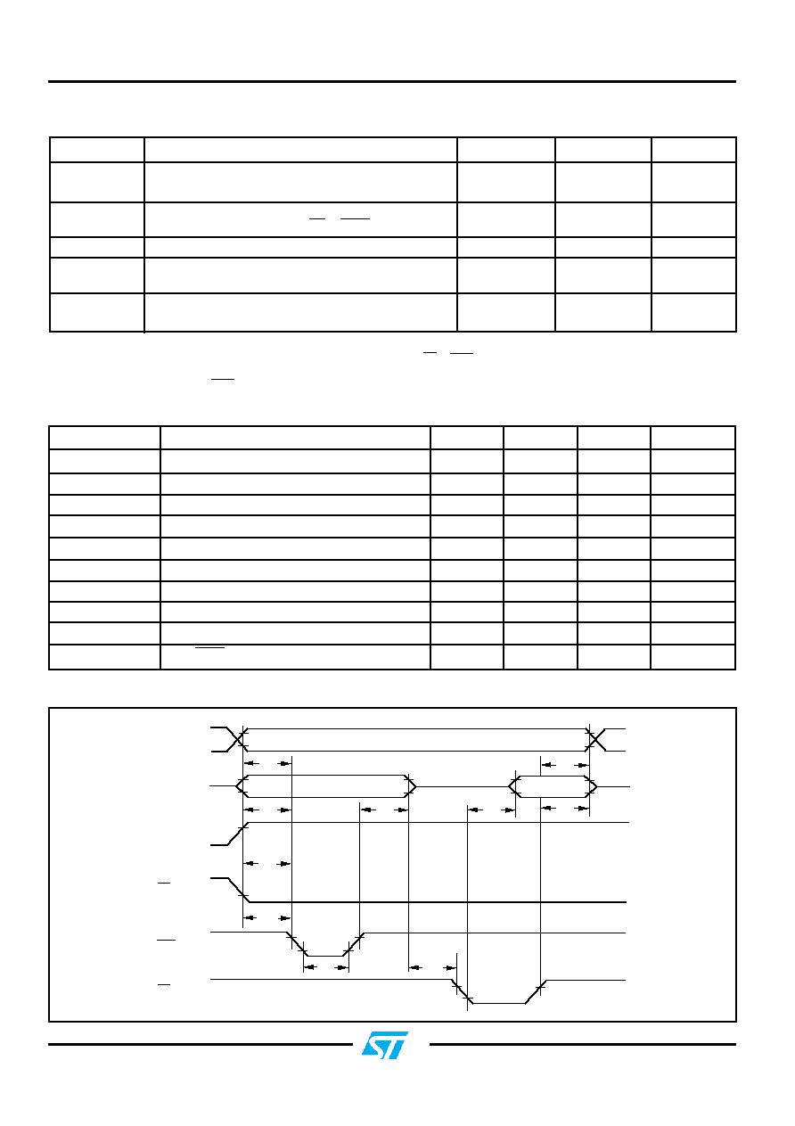
PROGRAMMING WAVEFORM
ADDRESS STABLE
ADDRESSES
V
PP
V
PP
V
CC
PGM
DATA
t
AS
t
PW
t
OS
t
OH
t
OE
t
AH
t
DF
t
VS
t
CES
t
OES
DATA OUT
DATA IN STABLE
OE
V
IH
V
IL
V
IH
V
IL
VALID
HIGH Z
CE
V
IH
V
IL

ORDERING INFORMATION
SPEED
PACKAGE
PACKAGE
OPERATING WSI
PART NUMBER
(ns)
TYPE
DRAWING
TEMPERATURE
MANUFACTURING
RANGE
PROCEDURE
WS57C128FB-35D
35
28 Pin CERDIP, 0.6"
D2
Comm'l
Standard
WS57C128FB-45D
45
28 Pin CERDIP, 0.6"
D2
Comm'l
Standard
WS57C128FB-45DMB
45
28 Pin CERDIP, 0.6"
D2
Military
MIL-STD-883C
WS57C128FB-45J
45
32 Pin PLDCC
J4
Comm'l
Standard
WS57C128FB-45L
45
32 Pin CLDCC
L3
Comm'l
Standard
WS57C128FB-55CMB
55
32 Pad CLLCC
C2
Military
MIL-STD-883C
WS57C128FB-55D
55
28 Pin CERDIP, 0.6"
D2
Comm'l
Standard
WS57C128FB-55DMB
55
28 Pin CERDIP, 0.6"
D2
Military
MIL-STD-883C
WS57C128FB-70D
70
28 Pin CERDIP, 0.6"
D2
Comm'l
Standard
WS57C128FB-70DM
70
28 Pin CERDIP, 0.6"
D2
Military
Standard
WS57C128FB-70DMB
70
28 Pin CERDIP, 0.6"
D2
Military
MIL-STD-883C
3-11
WS57C128FB
PROGRAMMING/ALGORITHMS/ERASURE/PROGRAMMERS
REFER TO
PAGE 5-1
The WS57C128FB is programmed using Algorithm D shown on page 5-9.
NOTE:
12. The actual part marking will not include the initials "WS."
Return to Main Menu