WS57C256F
3-13
V
CC
A14
A13
A8
A9
A11
OE
A10
CE/PGM
O
7
O
6
O
5
O
4
O
3
V
PP
A
12
A
7
A
6
A
5
A
4
A
3
A
2
A
1
A
0
O
0
O
1
O
2
GND
1
2
3
4
5
6
7
8
9
10
11
12
13
14
28
27
26
25
24
23
22
21
20
19
18
17
16
15
A
8
A
9
A
11
NC
OE
A
10
CE/PGM
O
7
O
6
A
6
A
5
A
4
A
3
A
2
A
1
A
0
NC
O
0
A
7
A
12
V
PP
NC
V
CC
A
14
A
13
O
1
O
2
NC
O
3
O
4
O
5
1
4 3
2
32 31 30
29
28
27
26
25
24
23
22
21
5
6
7
8
9
10
11
12
13
14 15 16 17 18 19 20
GND
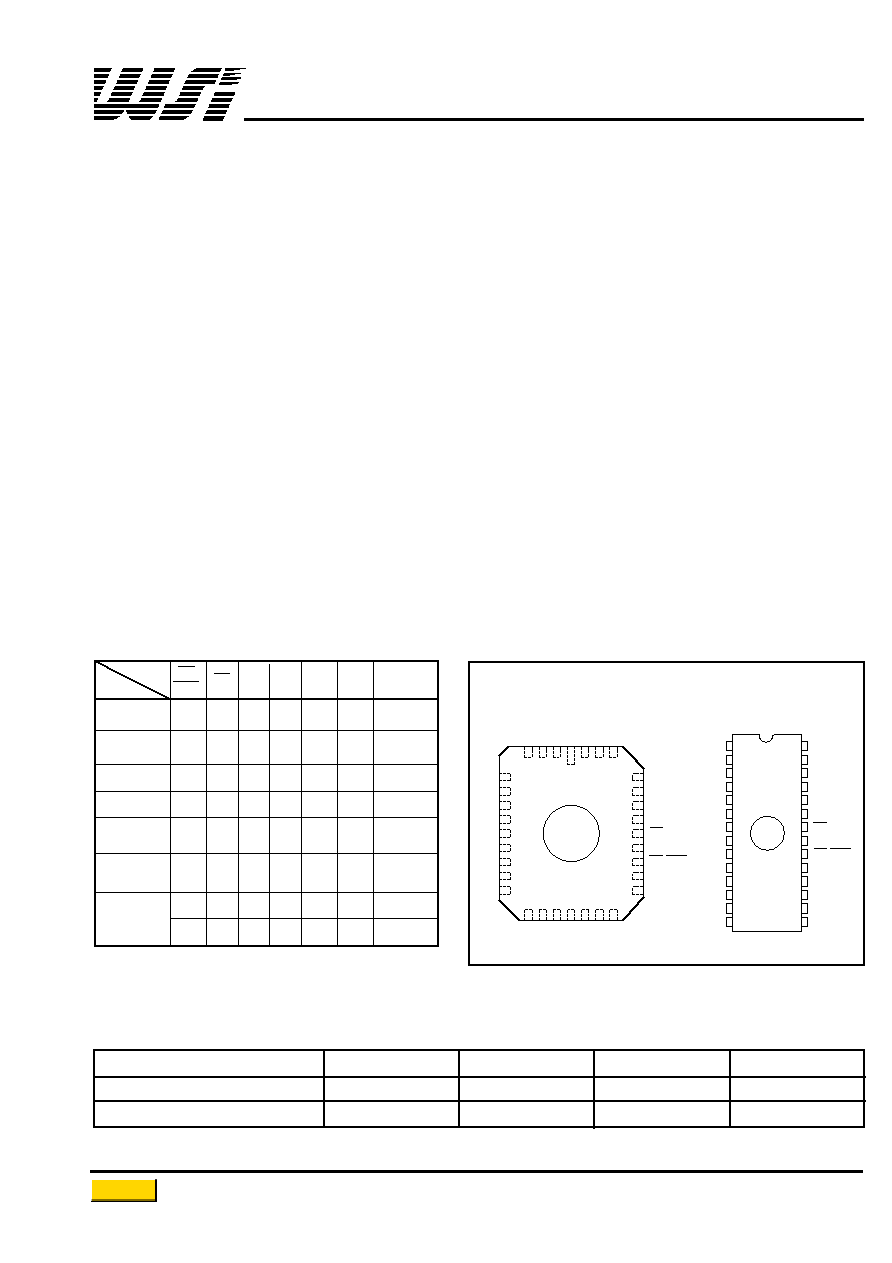
TOP VIEW
Chip Carrier
CERDIP
PIN CONFIGURATION
HIGH SPEED 32K x 8 CMOS EPROM
KEY FEATURES
�
Fast Access Time
�
Immune to Latch-UP
-- t
ACC
= 35 ns
-- Up to 200 mA
-- t
CE
= 35 ns
�
ESD Protection Exceeds 2000 Volts
�
Low Power Consumption
�
Available in 300 Mil DIP and PLDCC
-- 200 �A Standby I
CC
�
DESC SMD No. 5962-86063
GENERAL DESCRIPTION
The WS57C256F is a High Performance 32K x 8 UV Erasable EPROM. It is manufactured using an advanced
CMOS process technology enabling it to operate at speeds as fast as 35 ns Address Access Time (t
ACC
) and 35 ns
Chip Enable Time (t
CE
). It was designed utilizing WSI's patented self-aligned split gate EPROM cell, resulting in a
low power device with a very cost effective die size. The low standby power capability of this 256 K product (200 �A
in a CMOS interface environment) is especially attractive.
This product, with its high speed capability, is particularly appropriate for use with today's fast DSP processors and
high-clock-rate Microprocessors. The WS57C256F's 35 ns speed enables these advanced processors to operate
without introducing any undesirable wait states. The WS57C256F is also ideal for use in modem applications, and is
recommended for use in these applications by the leading modem chip set manufacturer.
The WS57C256F is available in a variety of package types including the space saving 300 Mil DIP, the surface
mount PLDCC, and other windowed and non-windowed options. And its standard JEDEC EPROM pinouts provide
for automatic upgrade density paths for current 64K and 128K EPROM users.
PINS
CE/
OE
A9
A0 VPP VCC OUTPUTS
MODE
PGM
Read
VIL
VIL
X
X
VCC VCC
DOUT
Output
Disable
X
VIH
X
X
VCC VCC
High Z
Standby
VIH
X
X
X
VCC VCC
High Z
Program
VIL
VIH
X
X
VPP
2
VCC
DIN
Program
Verify
X
VIL
X
X
VPP
2
VCC
DOUT
Program
Inhibit
VIH VIH
X
X
VPP
2
VCC
High Z
Signature
3
VIL
VIL VH
2
VIL VCC VCC
23 H
4
VIL
VIL VH
2
VIH VCC VCC
EO H
5
MODE SELECTION
NOTES:
1. X can be V
IL
or V
IH
.
4. Manufacturer Signature.
2. V
IH
= V
PP
= 12.75 � 0.25 V.
5. Device Signature.
3. A1 � A8, A10 � A14 = V
IL
.
PRODUCT SELECTION GUIDE
PARAMETER
WS57C256F-35
WS57C256F-45
WS57C256F-55
WS57C256F-70
Address Access Time (Max)
35 ns
45 ns
55 ns
70 ns
Output Enable Time (Max)
15 ns
20 ns
25 ns
30 ns
Return to Main Menu
DC READ CHARACTERISTICS
Over Operating Range with V
PP
= V
CC
SYMBOL
PARAMETER
TEST CONDITIONS
MIN
MAX
UNITS
V
IL
Input Low Voltage
(Note 4)
� 0.1
0.8
V
V
IH
Input High Voltage
(Note 4)
2.0
V
CC
+ 0.3
V
V
OL
Output Low Voltage
I
OL
= 16 mA
0.4
V
V
OH
Output High Voltage
I
OH
= � 4 mA
2.4
V
I
SB1
V
CC
Standby Current (CMOS)
CE = V
CC
� 0.3 V
Comm'l
200
�A
(Note 1)
Ind/Mil
500
�A
I
SB2
V
CC
Standby Current (TTL)
CE = V
IH
(Note 2)
Comm'l
3
mA
Ind/Mil
5
mA
I
CC1
V
CC
Active Current (CMOS)
(Notes 1 and 3)
Comm'l
25
mA
Outputs Not Loaded
Ind/Mil
30
mA
(Notes 2 and 3)
Comm'l
50
mA
I
CC2
V
CC
Active Current (TTL)
Outputs Not Loaded
Ind/Mil
60
mA
I
PP
V
PP
Supply Current
V
PP
= V
CC
100
�A
V
PP
V
PP
Read Voltage
V
CC
� 0.4
V
CC
V
I
LI
Input Leakage Current
V
IN
= 5.5V or Gnd
�10
10
�A
I
LO
Output Leakage Current
V
OUT
= 5.5 V or Gnd
�10
10
�A
AC READ CHARACTERISTICS
Over Operating Range. with V
PP
= V
CC
PARAMETER
SYMBOL
57C256F-35
57C256F-45
57C256F-55
57C256F-70
UNITS
MIN
MAX
MIN
MAX
MIN
MAX
MIN
MAX
Address to Output Delay
t
ACC
35
45
55
70
CE to Output Delay
t
CE
35
45
55
70
OE to Output Delay
t
OE
15
20
25
30
ns
Output Disable to Output Float
t
DF
20
20
25
30
Address to Output Hold
t
OH
0
0
0
0
OPERATING RANGE
RANGE
TEMPERATURE
V
CC
Commercial
0�C to +70�C
+5V � 10%
Industrial
�40�C to +85�C
+5V � 10%
Military
�55�C to +125�C
+5V � 10%
WS57C256F
3-14
ABSOLUTE MAXIMUM RATINGS*
Storage Temperature............................�65� to + 150�C
Voltage on any Pin with
Respect to Ground ....................................�0.6V to +7V
V
PP
and A
9
with Respect to Ground ......�0.6V to + 14V
ESD Protection ..................................................
>
2000V
*
NOTICE:
Stresses above those listed under "Absolute Maximum
Ratings" may cause permanent damage to the device.
This is a stress rating only and functional operation of
the device at these or any other conditions above
those indicated in the operational sections of this
specification is not implied. Exposure to absolute
maximum rating conditions for extended periods of
time may affect device reliability.
NOTES:
1. CMOS inputs: GND � 0.3V or V
CC
� 0.3V.
4. These are absolute voltages with respect to device ground pin and
2. TTL inputs: V
IL
0.8V, V
IH
2.0V.
include all overshoots due to system and/or tester noise.
3. Add 3 mA/MHz for A.C. power component.
Do not attempt to test these values without suitable equipment.
SYMBOL
PARAMETER
CONDITIONS
TYP
(6)
MAX
UNITS
C
IN
Input Capacitance
V
IN
= 0V
4
6
pF
C
OUT
Output Capacitance
V
OUT
= 0V
8
12
pF
C
VPP
V
PP
Capacitance
V
PP
= 0 V
18
25
pF
3-15
WS57C256F
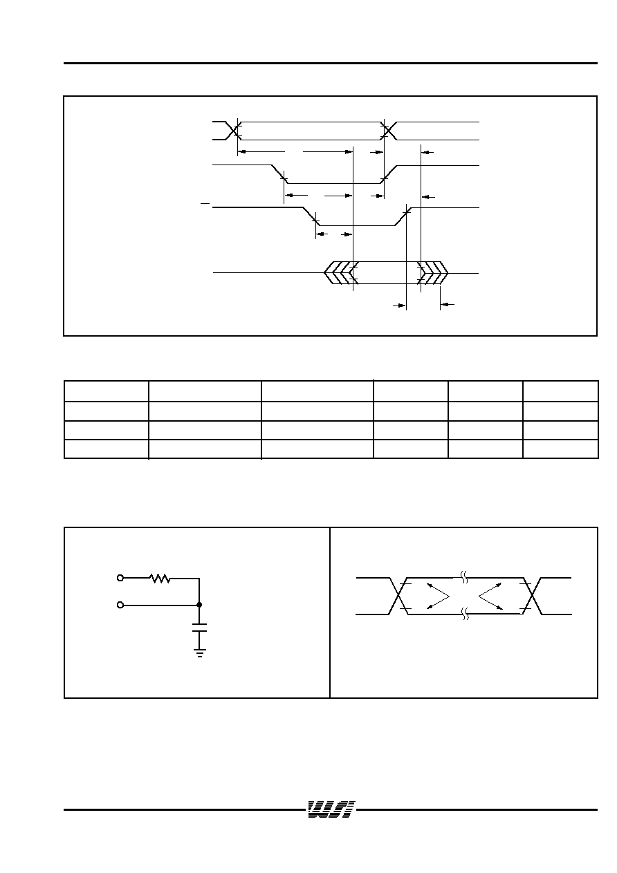
AC READ TIMING DIAGRAM
t
ACC
VALID
VALID
ADDRESSES
t
OE
t
DF
t
CE
CE
OE
t
OH
t
DF
OUTPUTS
CAPACITANCE
(5)
T
A
= 25�C, f = 1 MHz
A.C. TESTING INPUT/OUTPUT WAVEFORM
TEST LOAD
(High Impedance Test Systems)
3.0
0.0
2.0
0.8
2.0
0.8
TEST
POINTS
NOTE: 7. Provide adequate decoupling capacitance as close as possible to this device to achieve the published A.C. and D.C. parameters.
A 0.1 microfarad capacitor in parallel with a 0.01 microfarad capacitor connected between V
CC
and ground is recommended.
Inadequate decoupling may result in access time degradation or other transient performance failures.
NOTES: 5. This parameter is only sampled and is not 100% tested.
6. Typical values are for T
A
= 25�C and nominal supply voltages.
A.C. testing inputs are driven at 3.0 V for a logic "1" and 0.0 V
for a logic "0." Timing measurements are made at 2.0 V for a
logic "1" and 0.8 V for a logic "0".
30 pF
(INCLUDING SCOPE
AND JIG
CAPACITANCE)
98
2.01 V
D.U.T.

SYMBOLS
PARAMETER
MIN
TYP
MAX
UNITS
t
AS
Address Setup Time
2
�s
t
COH
CE High to OE High
2
�s
t
OES
Output Enable Setup Time
2
�s
t
OS
Data Setup Time
2
�s
t
AH
Address Hold Time
0
�s
t
OH
Data Hold Time
2
�s
t
DF
Chip Disable to Output Float Delay
0
130
ns
t
OE
Data Valid From Output Enable
130
ns
t
VS
/t
CES
V
PP
Setup Time/CE Setup Time
2
�s
t
PW
PGM Pulse Width
100
200
�s
t
OCX
OE Low to CE "Don't Care"
2
�s
WS57C256F
3-16
PROGRAMMING INFORMATION
DC CHARACTERISTICS
(T
A
= 25 � 5�C, V
CC
= 6.25 V � 0.25 V, V
PP
= 12.75 � 0.25 V)
SYMBOLS
PARAMETER
MIN
MAX
UNITS
I
LI
Input Leakage Current
�10
10
�A
(V
IN
= V
CC
or Gnd)
I
PP
V
PP
Supply Current During
60
mA
Programming Pulse (CE/ PGM = V
IL
)
I
CC
V
CC
Supply Current (Note 8)
35
mA
V
OL
Output Low Voltage During Verify
0.4
V
(I
OL
= 16 mA)
V
OH
Output High Voltage During Verify
2.4
V
(I
OH
= �4 mA)
AC CHARACTERISTICS
(T
A
= 25 � 5�C, V
CC
= 6.25 V � 0.25 V, V
PP
= 12.75 � 0.25 V)
PROGRAMMING WAVEFORM
ADDRESS STABLE
ADDRESSES
V
PP
V
PP
V
CC
CE/PGM
DATA
t
AS
t
PW
t
OS
t
OH
t
OE
t
AH
t
DF
t
VS
t
CES
t
OES
t
OCX
t
COH
DATA OUT
DATA IN STABLE
OE
V
IH
V
IL
V
IH
V
IL
VALID
HIGH Z
NOTE:
8. V
CC
must be applied either coincidentally or before V
PP
and removed either coincidentally or after V
PP
.
9. V
PP
must not be greater than 13 volts including overshoot. During CE = PGM = V
IL
, V
PP
must not be switched from 5 volts to
12.5 volts or vice-versa.
10. During power up the PGM pin must be brought high (
V
IH
) either coincident with or before power is applied to V
PP
.

ORDERING INFORMATION
OPERATING WSI
PART NUMBER
TEMPERATURE MANUFACTURING
RANGE
PROCEDURE
WS57C256F-35C
35
32 Pad CLLCC
C2
Comm'l
Standard
WS57C256F-35D
35
28 Pin CERDIP, 0.6"
D2
Comm'l
Standard
WS57C256F-35J
35
32 Pin PLDCC
J4
Comm'l
Standard
WS57C256F-35L
35
32 Pin CLDCC
L3
Comm'l
Standard
WS57C256F-35P
35
28 Pin Plastic DIP, 0.6"
P3
Comm'l
Standard
WS57C256F-35T
35
28 Pin CERDIP, 0.3"
T2
Comm'l
Standard
WS57C256F-45C
45
32 Pad CLLCC
C2
Comm'l
Standard
WS57C256F-45D
45
28 Pin CERDIP, 0.6"
D2
Comm'l
Standard
WS57C256F-45P
45
28 Pin Plastic DIP, 0.6"
P3
Comm'l
Standard
WS57C256F-45T
45
28 Pin CERDIP, 0.3"
T2
Comm'l
Standard
WS57C256F-55C
55
32 Pad CLLCC
C2
Comm'l
Standard
WS57C256F-55CMB
55
32 Pad CLLCC
C2
Military
MIL-STD-883C
WS57C256F-55D
55
28 Pin CERDIP, 0.6"
D2
Comm'l
Standard
WS57C256F-55DM
55
28 Pin CERDIP, 0.6"
D2
Military
Standard
WS57C256F-55DMB
55
28 Pin CERDIP, 0.6"
D2
Military
MIL-STD-883C
WS57C256F-55J
55
32 Pin PLDCC
J4
Comm'l
Standard
WS57C256F-55L
55
32 Pin CLDCC
L3
Comm'l
Standard
WS57C256F-55P
55
28 Pin Plastic DIP, 0.6"
P3
Comm'l
Standard
WS57C256F-55T
55
28 Pin CERDIP, 0.3"
T2
Comm'l
Standard
WS57C256F-55TMB
55
28 Pin CERDIP, 0.3"
T2
Military
MIL-STD-883C
WS57C256F-70CMB
*
70
32 Pad CLLCC
C2
Military
MIL-STD-883C
WS57C256F-70D
70
28 Pin CERDIP, 0.6"
D2
Comm'l
Standard
WS57C256F-70DMB
*
70
28 Pin CERDIP, 0.6"
D2
Military
MIL-STD-883C
WS57C256F-70J
70
32 Pin PLDCC
J4
Comm'l
Standard
WS57C256F-70JI
70
32 Pin PLDCC
J4
Industrial
Standard
WS57C256F-70T
70
28 Pin CERDIP, 0.3"
T2
Comm'l
Standard
SPEED
PACKAGE
PACKAGE
(ns)
TYPE
DRAWING
3-17
WS57C256F
NOTE: 11. The actual part marking will not include the initials "WS."
*
SMD product. See section 4 for DESC SMD number.
PROGRAMMING/ALGORITHMS/ERASURE/PROGRAMMERS
REFER TO
PAGE 5-1
The WS57C256F is programmed using Algorithm D shown on page 5-9.
When using Data I/O programmers, algorithm 57C256FB is recommended for use with the
WS57C256F for best programming results.
Return to Main Menu