
HIGH-SPEED 2K x 8 REGISTERED CMOS PROM/RPROM
KEY FEATURES
∑
Ultra-Fast Access Time
∑
DESC SMD Nos. 5962-88735/5962-87529
-- 25 ns Setup
∑
Pin Compatible with AM27S45 and
-- 12 ns Clock to Output
CY7C245
∑
Low Power Consumption
∑
Immune to Latch-UP
∑
Fast Programming
-- Up to 200 mA
∑
Programmable Synchronous or
∑
ESD Protection Exceeds 2000 V
Asynchronous Output Enable
∑
Programmable Asynchronous Initialize
Register
GENERAL DESCRIPTION
The WS57C45 is an extremely High Performance 16K UV Erasable Registered CMOS RPROM. It is a direct
drop-in replacement for such devices as the AM27S45 and CY7C245.
To meet the requirements of systems which execute and fetch instructions simultaneously, an 8-bit parallel data
register has been provided at the output which allows RPROM data to be stored while other data is being
addressed.
An asynchronous initialization feature has been provided which enables a user programmable 2049th word to be
placed on the outputs independent of the system clock. This feature can be used to force an initialize word or
provide a preset or clear function.
A further advantage of the WS57C45 over Bipolar PROM devices is the fact that it utilizes a proven EPROM
technology. This enables the entire memory array to be tested for switching characteristics and functionality after
assembly. Unlike devices which cannot be erased, every WS57C45 RPROM in a windowed package is 100%
tested with worst case test patterns both before and after assembly.
WS57C45
2-21
V
CC
A
8
A
9
A10
INIT/V
PP
OE/OE
S
CP/PGM
O
7
O
6
O
5
O
4
O
3
A
7
A
6
A
5
A
4
A
3
A
2
A
1
A
0
O
0
O
1
O
2
GND
A
10
INIT/V
PP
OE/OE
S
CP/PGM
NC
O
7
O
6
A
5
A
6
A
7
V
CC
A
8
A
9
NC
A
4
A
3
A
2
A
1
A
0
NC
O
0
O
1
O
2
NC O
3
O
4
O
5
GND
1
2
3
4
5
6
7
8
9
10
11
12
24
23
22
21
20
19
18
17
16
15
14
13
1
4 3
2
28 27 26
25
24
23
22
21
20
19
5
6
7
8
9
10
11
12 13 14 15 16 17 18
TOP VIEW
PIN CONFIGURATION
PRODUCT SELECTION GUIDE
PARAMETER
WS57C45-25
WS57C45-35
WS57C45-45
Set Up Time (Max)
25 ns
35 ns
45 ns
Clock to Output (Max)
12 ns
15 ns
25 ns
Chip Carrier
CERDIP/Plastic DIP/
Flatpack
Return to Main Menu
DC READ CHARACTERISTICS
Over Operating Range. (See Above)
SYMBOL
PARAMETER
TEST CONDITIONS
MIN
MAX
UNITS
V
OL
Output Low Voltage
I
OL
= 16 mA
0.4
V
V
OH
Output High Voltage
I
OH
= ≠4 mA
2.4
V
V
CC
= 5.5 V, f = 0 MHz (Note 1),
Comm'l
20
mA
I
CC1
V
CC
Active Current
Output Not Loaded
Industrial
30
mA
(CMOS)
Add 2 mA/MHz for AC Operation
Military
30
mA
V
CC
= 5.5 V, f = 0 MHz (Note 1),
Comm'l
25
mA
I
CC2
V
CC
Active Current
Output Not Loaded
Industrial
35
mA
(TTL)
Add 2 mA/MHz for AC Operation
Military
35
mA
I
LI
Input Leakage Current
V
IN
= 5.5V or Gnd
≠10
10
µA
I
LO
Output Leakage Current
V
OUT
= 5.5 V or Gnd
≠10
10
µA
SYMBOL
PARAMETER
CONDITIONS
MAX
UNITS
C
IN
Input Capacitance
T
A
= 25∞C, f = 1 MHz, V
CC
= 5.0 V
5
pF
C
OUT
Output Capacitance
8
pF
AC READ CHARACTERISTICS
Over Operating Range. (See Above)
PARAMETER
SYMBOL
WS57C45-25
WS57C45-35
WS57C45-45
UNITS
MIN
MAX
MIN
MAX
MIN
MAX
Address Setup to Clock High
t
SA
25
35
45
ns
Address Hold From Clock High
t
HA
0
0
0
ns
Clock High to Valid Output
t
CO
12
15
25
ns
Clock Pulse Width
t
PWC
15
20
20
ns
OE
S
Setup to Clock High
t
SOE
S
12
15
15
ns
OE
S
Hold From Clock High
t
HOE
S
5
5
5
ns
Delay From INIT to Valid Output
t
DI
20
20
35
ns
INIT Recovery to Clock High
t
RI
15
20
20
ns
INIT Pulse Width
t
PWI
15
20
25
ns
Active Output From Clock High
t
LZC
15
20
30
ns
Inactive Output From Clock High
t
HZC
15
20
30
ns
Active Output From OE Low
t
LZOE
15
20
30
ns
Inactive Output From OE High
t
HZOE
15
20
30
ns
OPERATING RANGE
RANGE
TEMPERATURE
V
CC
Commercial
0∞C to +70∞C
+5V ± 10%
Industrial
≠40∞C to +85∞C
+5V ± 10%
Military
≠55∞C to +125∞C
+5V ± 10%
WS57C45
2-22
ABSOLUTE MAXIMUM RATINGS*
Storage Temperature............................≠65∞ to + 150∞C
Voltage on any Pin with
Respect to Ground ................................≠0.6V to +7V
V
PP
with Respect to Ground...................≠0.6V to + 14V
ESD Protection ..................................................
>
2000V
NOTES:
1. CMOS inputs: GND ± 0.3V or V
CC
± 0.3V.
3. This parameter is only sampled and is not 100% tested.
2. TTL inputs: V
IL
0.8V, V
IH
2.0V.
*
NOTICE:
Stresses above those listed under "Absolute Maximum
Ratings" may cause permanent damage to the device.
This is a stress rating only and functional operation of
the device at these or any other conditions above
those indicated in the operational sections of this
specification is not implied. Exposure to absolute
maximum rating conditions for extended periods of
time may affect device reliability.
CAPACITANCE
(4)
2-23
WS57C45
A
10
OE/OE
S
O
7
O
6
O
5
O
4
O
3
O
2
O
1
O
0
INIT
ROW
DECODER
1 OF 64
A
9
A
8
A
7
A
6
A
5
A
4
A
3
A
2
A
1
A
0
CP
64
X
256
PROGRAMMABLE
ARRAY
8
X
1 OF 32
MULTIPLEXER
8-BIT
EDGE-
TRIGGERED
REGISTER
PROGRAMMABLE
INITIALIZE WORD
PROGRAMMABLE
MULTIPLEXER
COLUMN
DECODER
1 OF 32
D
C
Q
CP
OE
S
O
0
-O
7
A
0
-A
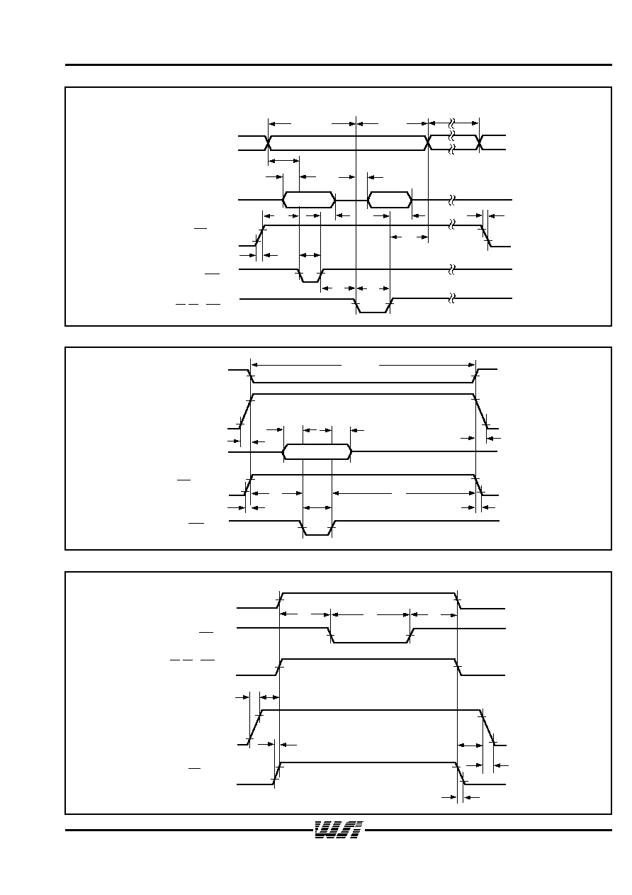
10
t
HA
t
PWC
t
PWC
t
PWI
t
PWC
t
PWC
t
PWC
t
PWC
t
SOE
S
t
SOE
S
t
SOE
S
t
HOE
S
t
HOE
S
t
HOE
S
t
HA
t
SA
t
CO
t
DI
t
RI
t
HZC
t
LZC
t
CO
t
HZOE
t
LZOE
INIT
OE
CP
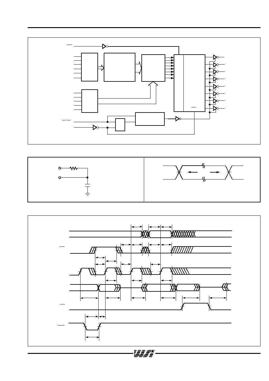
30 pF
(INCLUDING SCOPE
AND JIG
CAPACITANCE)
98
2.01 V
D.U.T.
3.0
0.0
1.5
1.5
TEST
POINTS
TEST LOAD
(High Impedance Test Systems)
A.C. TESTING INPUT/OUTPUT WAVEFORM
AC READ TIMING DIAGRAM
BLOCK DIAGRAM
A.C. testing inputs are driven at 3.0 V for a logic "1" and 0.0 V
for a logic "0." Timing measurements are made at 1.5 V for
input and output transitions in both directions.

WS57C45
2-24
1.2
1.1
1.0
0.9
0.8
-55 -35 -15
5
25
45
65
85
105 125
AMBIENT TEMPERATURE (∞C)
NORMALIZED I
CC
1.60
1.40
1.20
1.00
0.80
0.60
4.0
4.5
5.0
5.5
6.0
SUPPLY VOLTAGE ( V )
NORMALIZED I
CC
1.6
1.4
1.2
1.0
0.8
0.6
-55 -35
-15
5
25
45
65
85
105 125
AMBIENT TEMPERATURE (∞C)
NORMALIZED T
aa
40.0
35.0
30.0
25.0
20.0
15.0
10.0
5.0
0.0
0.0
200
400
600
800
1000
CAPACITANCE ( pF)
DELTA T
aa
(
ns
)
NORMALIZED SUPPLY CURRENT
vs.
SUPPLY VOLTAGE
TYPICAL ACCESS TIME CHANGE
vs.
OUTPUT LOADING
NORMALIZED Taa
vs.
AMBIENT TEMPERATURE
NORMALIZED SUPPLY CURRENT
vs.
AMBIENT TEMPERATURE

WS57C45
2-25
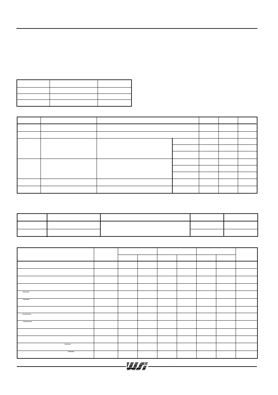
FUNCTION DESCRIPTION
The WS57C45 is an electrically programmable read only memory produced with WSI's patented high-performance
self-aligned split gate CMOS EPROM technology. It is organized as 2048 x 8 bits and is pin-for-pin compatible with
bipolar TTL fuse link PROMs. The WS57C45 includes a D-type 8-bit data register on-chip which reduces the
complexity and cost of microprogrammed pipelined systems where PROM data is held temporarily in a register. The
circuit features a programmable synchronous (OE
S
) or asynchronous (OE) output enable and asynchronous
initialization (INIT).
The programmed state of the enable pin (OE
S
or OE) will dictate the state of gthe outputs at power up. If OE
S
has
been programmed, the outputs will be in the OFF or high impedance state. If OE has been programmed, the
outputs will be OFF or high impedance only if the OE input is HIGH. Data is read by applying the address to inputs
A
10
≠ A
0
and a LOW to the enable input. The data is retrieved and loaded into the master section of the 8-bit data
register during the address set-up time. The data is transferred to the slave output of the data register at the next
LOW to HIGH clock (CP) transition. Then the output buffers present the data on the outputs (O
7
≠ O
0
).
When using the asynchronous enable (OE), the output buffers may be disabled at any time by switching the enable
input to a logic HIGH. They may be re-enabled by switching the enable to a logic LOW.
When using the sychronous enable (OE
S
), the outputs revert to a high impedance or OFF state at the next positive
clock edge following the OE
S
input transition to a HIGH state. The output will revert to the active state following a
positive clock edge when the OE
S
input is at a LOW state. The address and synchronous enable inputs are free to
change following a positive clock edge since the output will not change until the next low to high clock transition.
This enables accessing the next data location while previously addressed data is present on the outputs.
To avoid race conditions and simplify system timing, the 8-bit edge triggered data register clock is derived directly
from the system clock.
The WS57C45 has an asynchronous initialize input (INIT). This function can be used during power-up and time-out
periods to implement functions such as a start address or initialized bus control word. The INIT input enables the
contents of a 2049th 8-bit word to be loaded directly into the output data register. The INIT input can be used to
load any 8-bit data pattern into the register since each bit is programmable by the user. When unprogrammed,
activating INIT will result in clearing the register (outputs LOW). When all bits are programmed, actrivating INIT
results in PRESETting the register (outputs HIGH).
When activated LOW, the INIT input results in an immediate load of the 2049th word into both the master and slave
sections of the output register. This is independent of any other input including the clock (CP) input. The initialize
data will be present at the outputs after the asynchronous enable (OE) is taken to a LOW state.
Programming Information
Apply power to the WS57C45 for normal read mode operation with CP/PGM, OE/OE
S
and INIT/V
PP
at V
IH
. Then
take INIT/V
PP
to V
PP
. The part is then in the program inhibit mode operation and the output lines are in a high
impedance state. Refer to Figure 5. As shown in Figure 5, address, program and verify one byte of data. Repeat
this sequence for each location to be programmed.
When intelligent programming is used, the program pulse width is 1 ms in length. Each address location is
programmed and verified until it verifies correctly up to and including 5 times. After the location verifies, an
additional programming pulse should be applied that is X1 times in duration of the sum of the previous programming
pulses before proceeding on to the next address and repeating the process.
Initialization Byte Programming
The WS57C45 has a 2049th byte of data that can be used to initialize the value of the data register. This byte
contains the value "0" when it is shipped from the factory. The user must program the 2049th byte with a value other
than "0" for data register initialization if that value is not desired. Except for the following details, the user may
program the 2049th byte in the same manner as the other 2048 bytes. First, since all 2048 addresses are used up,
a super voltage address feature is used to enable an additional address. The actual address includes V
PP
on A
1
and V
IL
on A
2
. Refer to the Mode Selection table. The programming and verification of the Initial Byte is
accomplished operationally by performing an initialize function.

MODE
PIN FUNCTION
READ OR OUTPUT DISABLE
A
2
CP/PGM
(OE/OE
S
)/VFY
INIT/V
PP
A
1
OUTPUTS
Read (Note 6)
X
X
V
IL
V
IH
X
Data Out
Output Disable
X
X
V
IH
V
IH
X
High Z
Program (Notes 5 & 7)
X
V
IL
V
IH
V
PP
X
Data In
Program Verify (Notes 5 & 7)
X
V
IH
V
IL
V
PP
X
Data Out
Program Inhibit (Notes 5 & 7)
X
V
IH
V
IH
V
PP
X
High Z
Intelligent Program (Notes 5 & 7)
X
V
IL
V
IH
V
PP
X
Data In
Program Synch Enable (Note 7)
V
IH
V
IL
V
IH
V
PP
V
PP
High Z
Program Initial Byte (Note 7)
V
IL
V
IL
V
IH
V
PP
V
PP
Data In
Initial Byte Read
X
X
V
IL
V
IL
X
Data Out
WS57C45
2-26
NOTES: 5. X = Don't Care but not to exceed V
PP
.
6. During read operation, the output latches are loaded on a "0" to "1" transition of CP.
7. During programming and verification, all unspecified pins to be at V
IL.
Synchronous Enable Programming
The WS57C45 contains both a synchronous and asynchronous enable feature. The part is delivered configured in
the asynchronous mode and only requires alteration if the synchronous mode is required. This is accomplished by
programming an on-chip EPROM cell. Similar to the Initial Byte, this function is enabled and addressed by using a
super voltage. Referring to the Mode Selection table, V
PP
is applied to A
1
followed by V
IH
applied to A
2
. This
procedure addresses the EPROM cell that programs the synchronous enable feature. The EPROM cell is
programmed with a 10 ms program pulse on CP/PGM. It does not require any data since there is no selection as to
how synchronous enable may be programmed, only if it is to be programmed.
Synchronous Enable Verification
The WS57C45's synchronous enable function is verified operationally. Apply power for read operation with OE/OE
S
and INIT/V
PP
at V
IH
and take the clock (CP/PGM) from V
IL
to V
IH
. The output data bus should be in a high
impedance state. Next take OE/OE
S
to V
IL
. The outputs will remain in the high impedance state. Take the clock
(CP/PGM) from V
IL
to V
IH
and the outputs will now contain the data that is present. Take OE/OE
S
to V
IH
. The output
should remain driven. Clocking CP/PGM once more from V
IL
to V
IH
should place the outputs again in a high
impedance state.
Blank Check
Upon delivery from WaferScale Integration, Inc. or after each erasure (see Erasure section), the WS57C45 has all
2048 bytes in the `0' state. "1's" are loaded into the WS57C45 through the procedure of programming.
WS57C45
2-27
PROGRAM
VERIFY
DATA IN
DATA OUT
PROGRAM
OTHER BYTES
ADDRESS
DATA
CP/PGM
INIT/V
PP
(OE /OE
S
) / VFY
t
AS
t
DV
t
DS
V
IH
V
IH
V
IH
V
IL
V
IL
V
IL
V
PP
V
IL
V
IL
V
IH
V
IH
t
AS
t
R
t
F
t
DH
t
DZ
t
PW
t
DV
t
VP
t
AH
ADDRESS STABLE
FIGURE 5. PROM PROGRAMMING WAVEFORMS
DATA IN
PROGRAM
CP/PGM
V
IH
V
IL
V
PP
DATA
V
IH
V
IH
V
IL
V
IL
t
AH
t
DH
t
F
t
F
t
DS
t
AS
V
PP
V
IH
V
IH
V
IL
V
IL
A
2
A
1
t
R
t
R
t
PW
INIT/V
PP
FIGURE 6. INITIAL BYTE PROGRAMMING WAVEFORMS
CP/PGM
(OE /OE
S
) / VFY
t
AS
t
PW
V
IH
V
IH
V
IH
V
IH
A
1
A
2
V
PP
t
AS
V
PP
V
IH
t
R
t
R
t
F
t
F
V
IL
V
IL
V
IL
V
IL
V
IL
t
AH
t
AH
INIT/V
PP
FIGURE 7. PROGRAM SYNCHRONOUS ENABLE

WS57C45
2-28
SYMBOLS
PARAMETER
MIN
MAX
UNITS
I
LI
Input Leakage Current
≠10
10
µA
(V
IN
= V
CC
or Gnd)
I
PP
V
PP
Supply Current During
60
mA
Programming Pulse
I
CC
V
CC
Supply Current
25
mA
V
IL
Input Low Voltage
≠0.1
0.8
V
V
IH
Input High Voltage
2.0
V
CC
+ 0.3
V
V
OL
Output Low Voltage During Verify
0.45
V
(I
OL
= 16 mA)
V
OH
Output High Voltage During Verify
2.4
V
(I
OH
= ≠4 mA)
SYMBOLS
PARAMETER
MIN
MAX
UNITS
t
PW
Programming Pulse Width
0.1
10
ms
t
AS
Address Setup Time
1.0
µs
t
DS
Data Setup Time
1.0
µs
t
AH
Address Hold Time
1.0
µs
t
DH
Data Hold Time
1.0
µs
t
R,
t
F
V
PP
Rise and Fall Time
1.0
µs
t
VD
Delay to VFY
1.0
µs
t
VP
VFY Pulse Width
2.0
µs
t
DV
VFY Data Valid
1.0
µs
t
DZ
VFY HIGH to High Z
1.0
µs
NOTE: 8. V
PP
must not be greater than 14 volts including overshoot.
AC CHARACTERISTICS
(T
A
= 25 ± 5∞C, V
CC
= 5.6 V ± 0.25 V, V
PP
= 13.5 ± 0.5 V)
PROGRAMMING INFORMATION
DC CHARACTERISTICS
(T
A
= 25 ± 5∞C, V
CC
= 5.6 V ± 0.25 V, V
PP
= 13.5 ± 0.5 V)
ORDERING INFORMATION
SPEED
PACKAGE
PACKAGE
OPERATING WSI
PART NUMBER
(ns)
TYPE
DRAWING
TEMPERATURE MANUFACTURING
RANGE
PROCEDURE
WS57C45-25T
25
24 Pin CERDIP, 0.3"
T1
Comm'l
Standard
WS57C45-35KMB
*
35
24 Pin CERDIP, 0.3"
K1
Military
MIL-STD-883C
WS57C45-35S
35
24 Pin Plastic DIP, 0.3"
S1
Comm'l
Standard
WS57C45-35T
35
24 Pin CERDIP, 0.3"
T1
Comm'l
Standard
WS57C45-35TMB
*
35
24 Pin CERDIP, 0.3"
T1
Military
MIL-STD-883C
WS57C45-45KMB
*
45
24 Pin CERDIP, 0.3"
K1
Military
MIL-STD-883C
WS57C45-45TMB
*
45
24 Pin CERDIP, 0.3"
T1
Military
MIL-STD-883C
2-29
PROGRAMMING/ALGORITHMS/ERASURE/PROGRAMMERS
REFER TO
PAGE 5-1
The WS57C45 is programmed using Algorithm A shown on page 5-3.
NOTE: The actual part marking will not include the initials "WS."
*
SMD product. See section 4 for DESC SMD numbers.
WS57C45
Return to Main Menu