PRODUCT SELECTION GUIDE
PARAMETER
WS57C71C-35
WS57C71C-45
WS57C71C-55
WS57C71C-70
Address Access Time (Max)
35 ns
45 ns
55 ns
70 ns
CS to Output Valid Time (Max)
15 ns
20 ns
20 ns
30 ns
WS57C71C
2-55
HIGH SPEED 32K x 8 CMOS PROM/RPROM
KEY FEATURES
∑
Ultra-Fast Access Time
∑
Immune to Latch-UP
-- 35 ns
-- Up to 200 mA
∑
Low Power Consumption
∑
ESD Protection Exceeds 2000V
∑
Fast Programming
∑
Available in 300 Mil DIP and PLDCC
GENERAL DESCRIPTION
The WS57C71C is a High Performance 256K UV Erasable Electrically Re-Programmable Read Only Memory
(RPROM). It is manufactured in an advanced CMOS technology and utilizes WSI's patented self-aligned split gate
EPROM cell.
The industry standard PROM pin configuration of the WS57C71C provides an easy upgrade path from a 16K x 8
device.
This RPROM is capable of operating at speeds as fast as 35 ns address access time, which enables it to be used
directly with today's fast microprocessors and DSP processors without introducing any wait states. All inputs and
outputs are TTL compatible. The WS57C71C is a low power device even when operated at its fastest speed. The
DIP version is packaged in a 300 mil wide DIP package saving board space for the user.
V
CC
A10
A11
A12
A13
A14
CS3
CS2
CS1/VPP
O
7
O
6
O
5
O
4
O
3
A
9
A
8
A
7
A
6
A
5
A
4
A
3
A
2
A
1
A
0
O
0
O
1
O
2
GND
1
2
3
4
5
6
7
8
9
10
11
12
13
14
28
27
26
25
24
23
22
21
20
19
18
17
16
15
A
12
A
13
A
14
NC
CS3
CS2
CS1/VPP
O
7
O
6
A
6
A
5
A
4
A
3
A
2
A
1
A
0
NC
O
0
A
7
A
8
A
9
NC
V
CC
A
10
A
11
O
1
O
2
NC O
3
O
4
O
5
1
4 3
2
32 31 30
29
28
27
26
25
24
23
22
21
5
6
7
8
9
10
11
12
13
14 15 16 17 18 19 20
GND
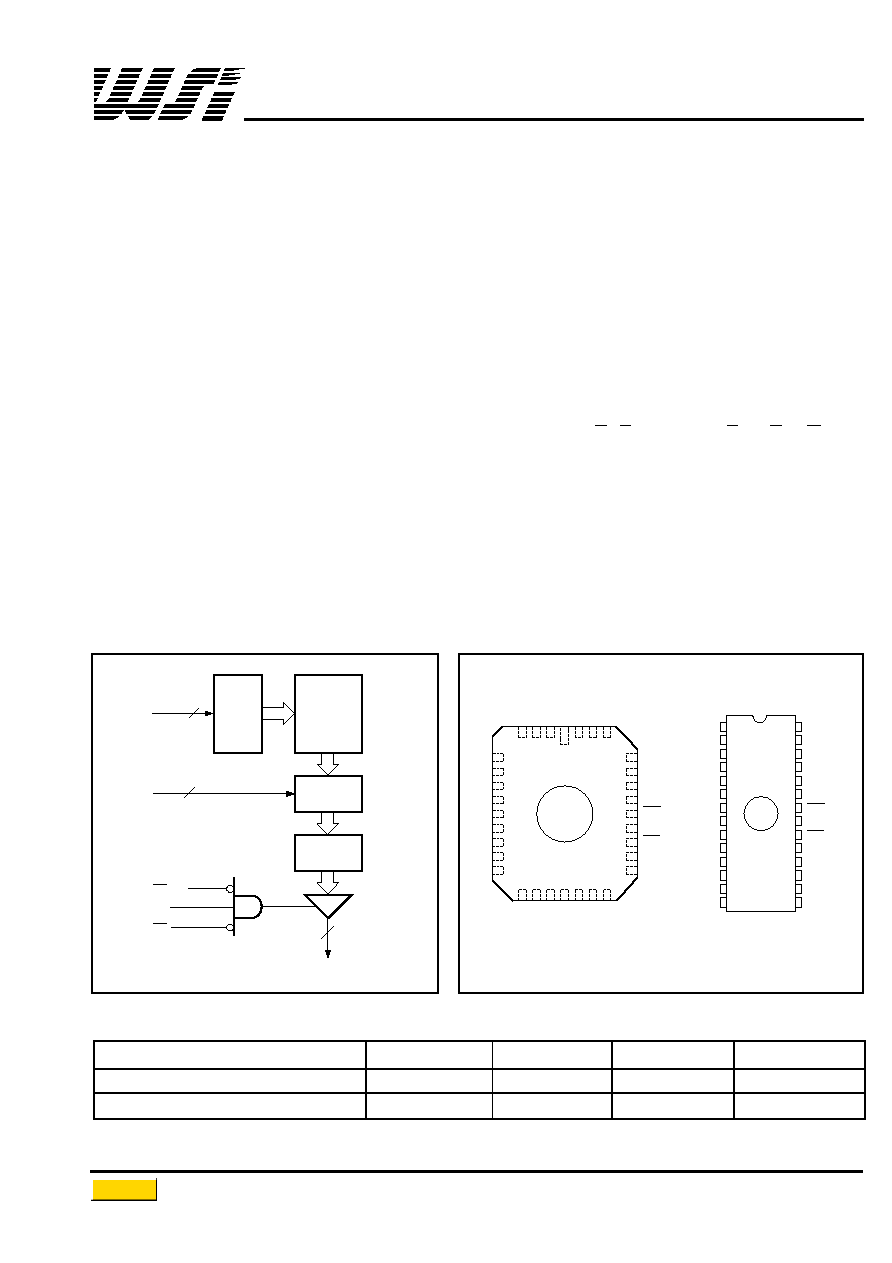
TOP VIEW
Chip Carrier
CERDIP
PIN CONFIGURATION
ROW
DECODER
EPROM ARRAY
262,144 BITS
COLUMN
DECODER
SENSE
AMPLIFIERS
8
CS2
CS3
OUTPUTS
CS1/ V
PP
A0 - A5
COLUMN
ADDRESSES
A6 - A14
ROW
ADDRESSES
9
9
BLOCK DIAGRAM
Return to Main Menu

WS57C71C
2-56
OPERATING RANGE
RANGE
TEMPERATURE
V
CC
Commercial
0∞C to +70∞C
+5V ± 10%
Industrial
≠40∞C to +85∞C
+5V ± 10%
Military
≠55∞C to +125∞C
+5V ± 10%
ABSOLUTE MAXIMUM RATINGS*
Storage Temperature............................≠65∞ to + 150∞C
Voltage on any Pin with
Respect to Ground ....................................≠0.6V to +7V
V
PP
with Respect to Ground...................≠0.6V to + 13V
ESD Protection ..................................................
>
2000V
*
NOTICE:
Stresses above those listed under "Absolute Maximum
Ratings" may cause permanent damage to the device.
This is a stress rating only and functional operation of
the device at these or any other conditions above
those indicated in the operational sections of this
specification is not implied. Exposure to absolute
maximum rating conditions for extended periods of
time may affect device reliability.
PINS
CS1/
CS2 CS3
V
CC
OUTPUTS
MODE
V
PP
Read
V
IL
V
IH
V
IL
V
CC
D
OUT
Output Disable
V
IH
X
X
V
CC
High Z
Output Disable
X
V
IL
X
V
CC
High Z
Output Disable
X
X
V
IH
V
CC
High Z
Program
V
PP
X
V
IH
V
CC
D
IN
Program Verify
V
IL
V
IH
V
IL
V
CC
D
OUT
Program Inhibit
V
PP
V
IH
V
IL
V
CC
D
OUT
MODE SELECTION
NOTES:
1. CMOS inputs: GND ± 0.3V or V
CC
± 0.3V.
2. TTL inputs: V
IL
0.8V, V
IH
2.0V.
3. These are absolute voltages with respect to device ground pin and include all overshoots due to system and/or tester noise.
Do not attempt to test these values without suitable equipment.
DC READ CHARACTERISTICS
Over Operating Range. (See Above)
SYMBOL
PARAMETER
TEST CONDITIONS
MIN
MAX
UNITS
V
IL
Input Low Voltage
(Note 3)
≠0.1
0.8
V
V
IH
Input High Voltage
(Note 3)
2.0
V
CC
+ 0.3
V
V
OL
Output Low Voltage
I
OL
= 16 mA
0.4
V
V
OH
Output High Voltage
I
OH
= ≠4 mA
2.4
V
V
CC
= 5.5 V, f = 0 MHz (Note 1),
Comm'l
30
mA
I
CC1
V
CC
Active Current
Output Not Loaded
Industrial
35
mA
(CMOS)
Add 3 mA/MHz for AC Operation
Military
35
mA
V
CC
= 5.5 V, f = 0 MHz (Note 2),
Comm'l
50
mA
I
CC2
V
CC
Active Current
Output Not Loaded
Industrial
60
mA
(TTL)
Add 3 mA/MHz for AC Operation
Military
60
mA
I
LI
Input Leakage
Current
V
IN
= 5.5V or Gnd
≠10
10
µA
I
LO
Output Leakage
Current
V
OUT
= 5.5 V or Gnd
≠10
10
µA
WS57C71C
2-57
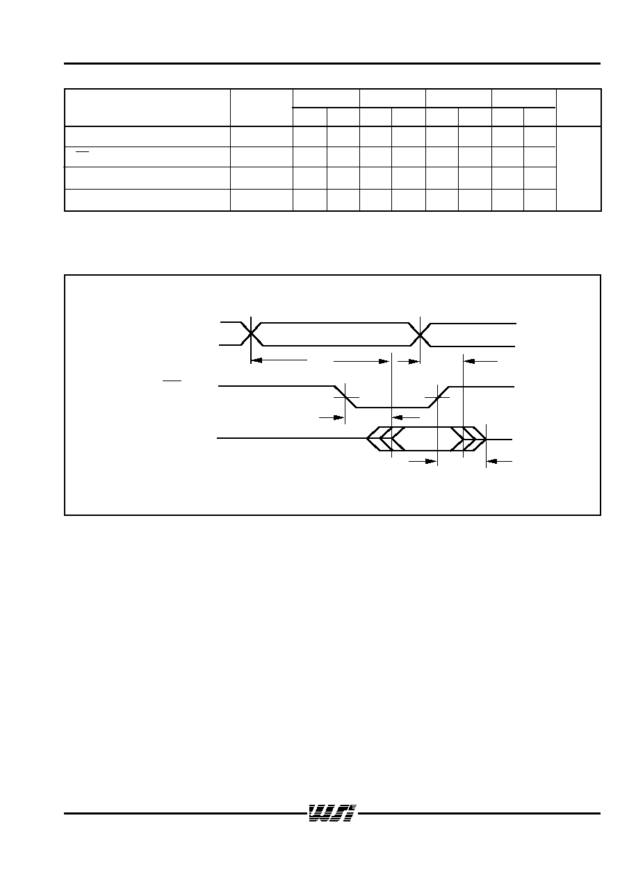
AC READ CHARACTERISTICS
Over Operating Range. (See Above)
PARAMETER
SYMBOL
57C71C-35
57C71C-45
57C71C-55
57C71C-70
UNITS
MIN
MAX
MIN
MAX
MIN
MAX
MIN
MAX
Address to Output Delay
t
ACC
35
45
55
70
CS to Output Delay
t
CS
15
20
20
30
ns
Output Disable to Output Float
*
t
DF
20
20
20
25
Address to Output Hold
t
OH
0
0
0
0
*
Sampled, Not 100% Tested.
AC READ TIMING DIAGRAM
VALID
ADDRESSES
OUTPUTS
t
ACC
t
OH
t
CS
t
DF
VALID
CSX, CS2
WS57C71C
2-58
SYMBOL
PARAMETER
CONDITIONS
TYP
(5)
MAX
UNITS
C
IN
Input Capacitance
V
IN
= 0V
4
6
pF
C
OUT
Output Capacitance
V
OUT
= 0V
8
12
pF
C
VPP
V
PP
Capacitance
V
PP
= 0 V
18
25
pF
CAPACITANCE
(4)
T
A
= 25∞C, f = 1 MHz
30 pF
(INCLUDING SCOPE
AND JIG
CAPACITANCE)
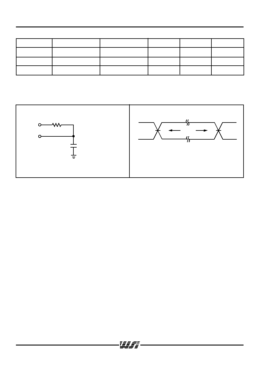
98
2.01 V
D.U.T.
A.C. TESTING INPUT/OUTPUT WAVEFORM
TEST LOAD
(High Impedance Test Systems)
3.0
0.0
1.5
1.5
TEST
POINTS
NOTE: 6. Provide adequate decoupling capacitance as close as possible to this device to achieve the published A.C. and D.C. parameters.
A 0.1 microfarad capacitor in parallel with a 0.01 microfarad capacitor connected between V
CC
and ground is recommended.
Inadequate decoupling may result in access time degradation or other transient performance failures.
NOTES: 4. This parameter is only sampled and is not 100% tested.
5.Typical values are for T
A
= 25∞C and nominal supply voltages.
A.C. testing inputs are driven at 3.0 V for a logic "1" and 0.0 V
for a logic "0." Timing measurements are made at 1.5 V for
input and output transitions in both directions.
2-59
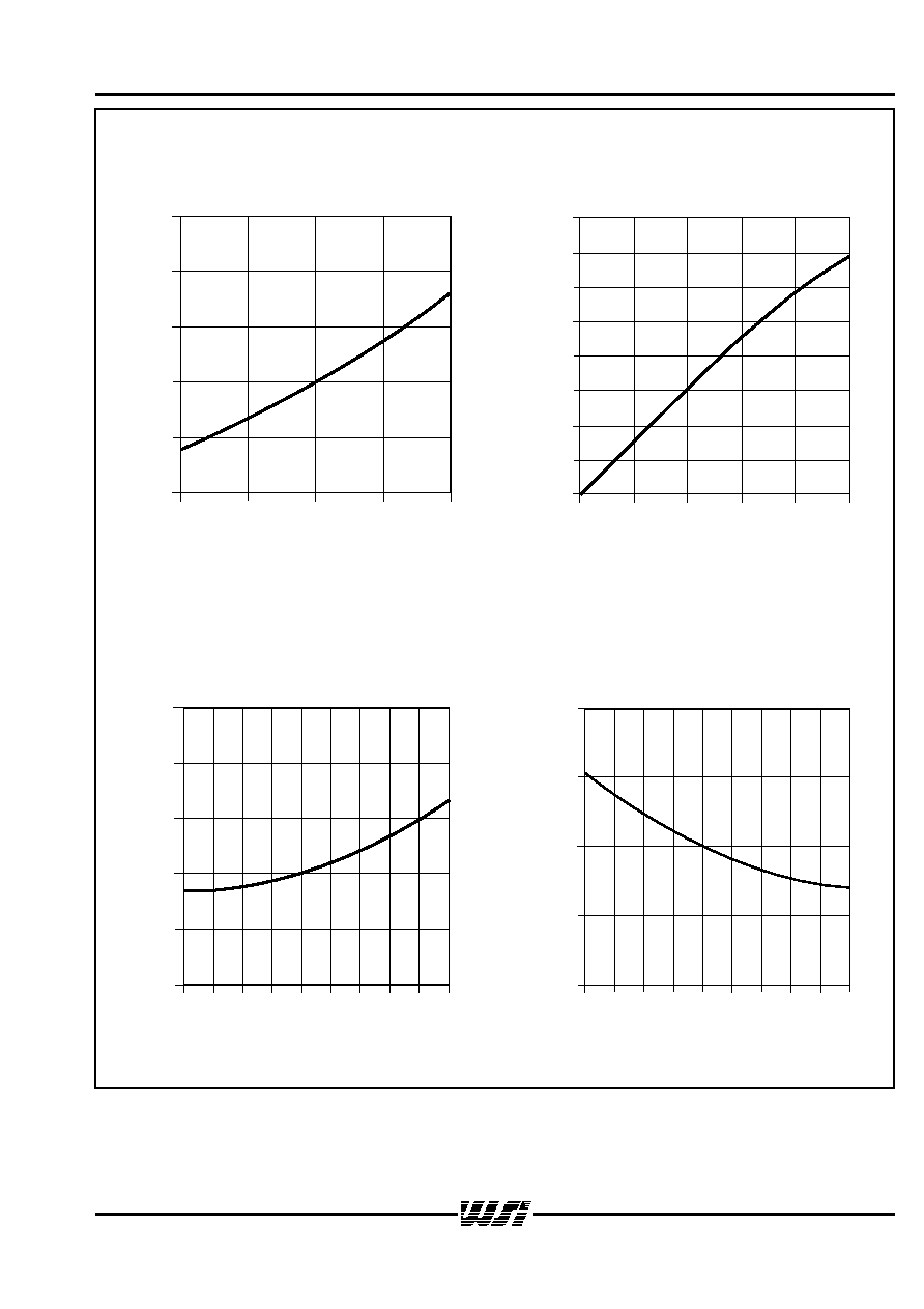
WS57C71C
1.2
1.1
1.0
0.9
0.8
-55 -35 -15
5
25
45
65
85
105 125
AMBIENT TEMPERATURE (∞C)
NORMALIZED I
CC
1.60
1.40
1.20
1.00
0.80
0.60
4.0
4.5
5.0
5.5
6.0
SUPPLY VOLTAGE ( V )
NORMALIZED I
CC
1.6
1.4
1.2
1.0
0.8
0.6
-55 -35
-15
5
25
45
65
85
105 125
AMBIENT TEMPERATURE (∞C)
NORMALIZED T
aa
40.0
35.0
30.0
25.0
20.0
15.0
10.0
5.0
0.0
0.0
200
400
600
800
1000
CAPACITANCE ( pF)
DELTA T
aa
(
ns
)
NORMALIZED SUPPLY CURRENT
vs.
SUPPLY VOLTAGE
TYPICAL ACCESS TIME CHANGE
vs.
OUTPUT LOADING
NORMALIZED Taa
vs.
AMBIENT TEMPERATURE
NORMALIZED SUPPLY CURRENT
vs.
AMBIENT TEMPERATURE