 | –≠–ª–µ–∫—Ç—Ä–æ–Ω–Ω—ã–π –∫–æ–º–ø–æ–Ω–µ–Ω—Ç: X02 | –°–∫–∞—á–∞—Ç—å:  PDF PDF  ZIP ZIP |
1/6
Æ
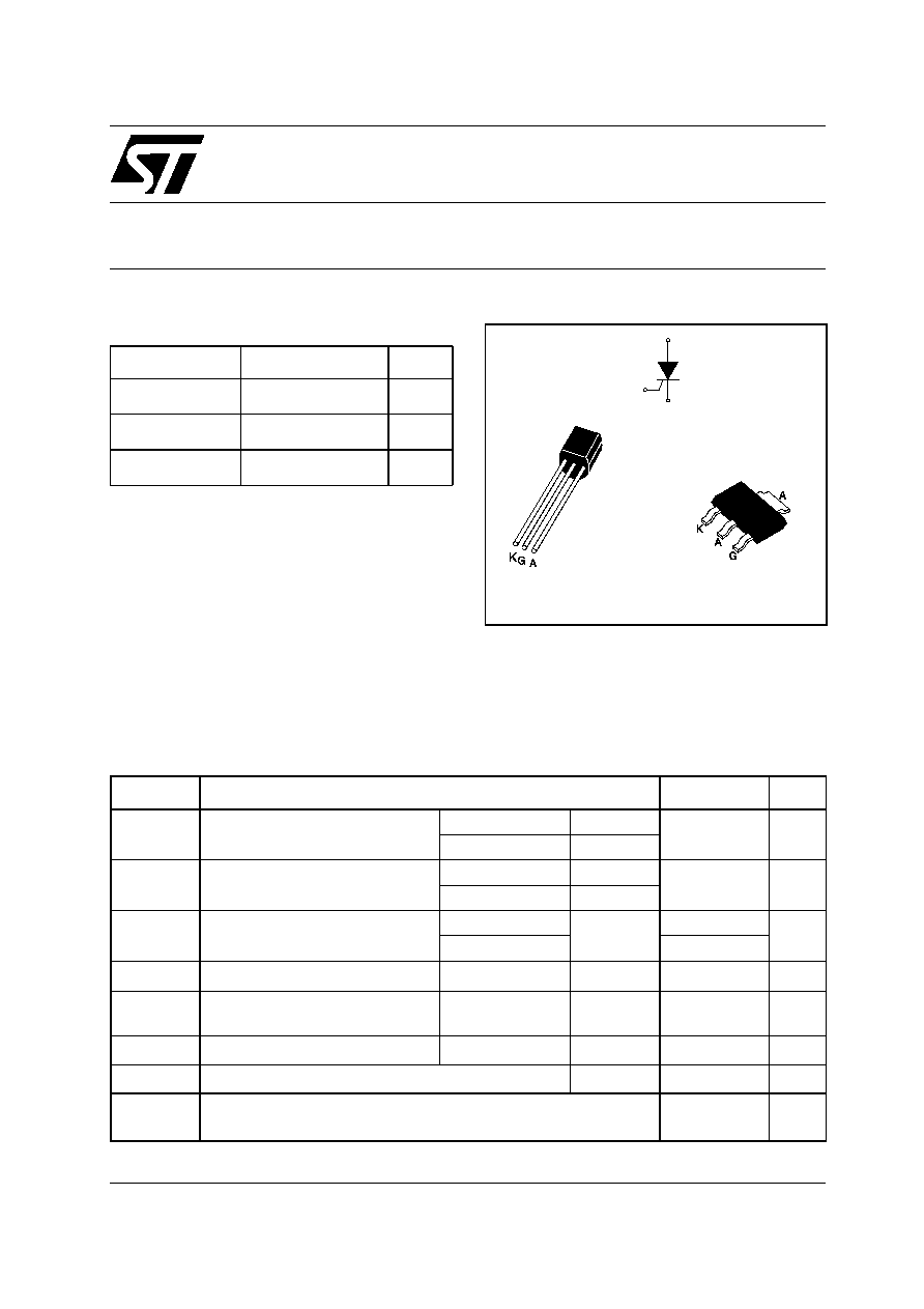
X02 Series
SENSITIVE
1.25A SCRs
September 2000 - Ed: 3
MAIN FEATURES:
DESCRIPTION
Thanks to highly sensitive triggering levels, the
X02 SCR series is suitable for all applications
where the available gate current is limited, such as
ground fault circuit interruptors, overvoltage
crowbar protection in low power supplies,
capacitive ignition circuits, ...
Available in though-hole or surface-mount
packages, these devices are optimized in forward
voltage drop and inrush current capabilities, for
reduced power losses and high reliability in harsh
environments.
Symbol
Value
Unit
I
T(RMS)
1.25
A
V
DRM
/V
RRM
600 and 800
V
I
GT
50 to 200
µA
ABSOLUTE RATINGS (limiting values)
Symbol
Parameter
Value
Unit
I
T(RMS)
RMS on-state current
(180∞ conduction angle)
TO-92
TI = 55∞C
1.25
A
SOT-223
Ttab = 95∞C
IT
(AV)
Average on-state current
(180∞ conduction angle)
TO-92
TI = 55∞C
0.8
A
SOT-223
Ttab = 95∞C
I
TSM
Non repetitive surge peak on-state
current
tp = 8.3 ms
Tj = 25∞C
25
A
tp = 10 ms
22.5
I
≤
t
I
≤
t Value for fusing
tp = 10 ms
Tj = 25∞C
2.5
A
2
S
dI/dt
Critical rate of rise of on-state current
I
G
= 2 x I
GT
, tr
100 ns
F = 60 Hz
Tj = 125∞C
50
A/µs
I
GM
Peak gate current
tp = 20 µs
Tj = 125∞C
1.2
A
P
G(AV)
Average gate power dissipation
Tj = 125∞C
0.2
W
T
stg
Tj
Storage junction temperature range
Operating junction temperature range
- 40 to + 150
- 40 to + 125
∞C
G
A
K
TO-92
(X02xxA)
SOT-223
(X02xxN)
X02 Series
2/6
ELECTRICAL CHARACTERISTICS (Tj = 25∞C, unless otherwise specified)
THERMAL RESISTANCES
S = Copper surface under tab
PRODUCT SELECTOR
Symbol
Test Conditions
X02xx
Unit
02
05
I
GT
V
D
= 12 V R
L
= 140
MIN.
-
20
µA
MAX.
200
50
V
GT
MAX.
0.8
V
V
GD
V
D
= V
DRM
R
L
= 3.3 k
R
GK
= 1 k
Tj = 125∞C
MIN.
0.1
V
V
RG
I
RG
= 10 µA
MIN.
8
V
I
H
I
T
= 50 mA R
GK
= 1 k
MAX.
5
mA
I
L
I
G
= 1 mA R
GK
= 1 k
MAX.
6
mA
dV/dt
V
D
= 67 % V
DRM
R
GK
= 1 k
Tj = 110∞C
MIN.
10
15
V/µs
V
TM
I
TM
= 2.5 A tp = 380 µs
Tj = 25∞C
MAX.
1.45
V
V
to
Threshold voltage
Tj = 125∞C
MAX.
0.9
V
R
d
Dynamic resistance
Tj = 125∞C
MAX.
200
m
I
DRM
I
RRM
V
DRM
= V
RRM
R
GK
= 1 k
Tj = 25∞C
MAX.
5
µA
Tj = 125∞C
500
Symbol
Parameter
Value
Unit
R
th(j-l)
Junction to leads (DC)
TO-92
60
∞C/W
R
th(j-t)
Junction to tab (DC)
SOT-223
25
R
th(j-a)
Junction to ambient (DC)
TO-92
150
S = 5 cm
≤
SOT-223
60
Part Number
Voltage
Sensitivity
Package
600 V
800 V
X0202MA
X
200 µA
TO-92
X0202MN
X
200 µA
SOT-223
X0202NA
X
200 µA
TO-92
X0202NN
X
200 µA
SOT-223
X0205MA
X
50 µA
TO-92
X0205MN
X
50 µA
SOT-223
X0205NA
X
50 µA
TO-92
X0205NN
X
50 µA
SOT-223
X02 Series
3/6
ORDERING INFORMATION
OTHER INFORMATION
Note: xx = sensitivity, y = voltage
Part Number
Marking
Weight
Base Quantity
Packing mode
X02xxyA 1BA2
X02xxyA
0.2 g
2500
Bulk
X02xxyA 2BL2
X02xxyA
0.2 g
2000
Ammopack
X0202yN 5BA4
X2y
0.12 g
1000
Tape & reel
X0205yN 5BA4
X5y
0.12 g
1000
Tape & reel
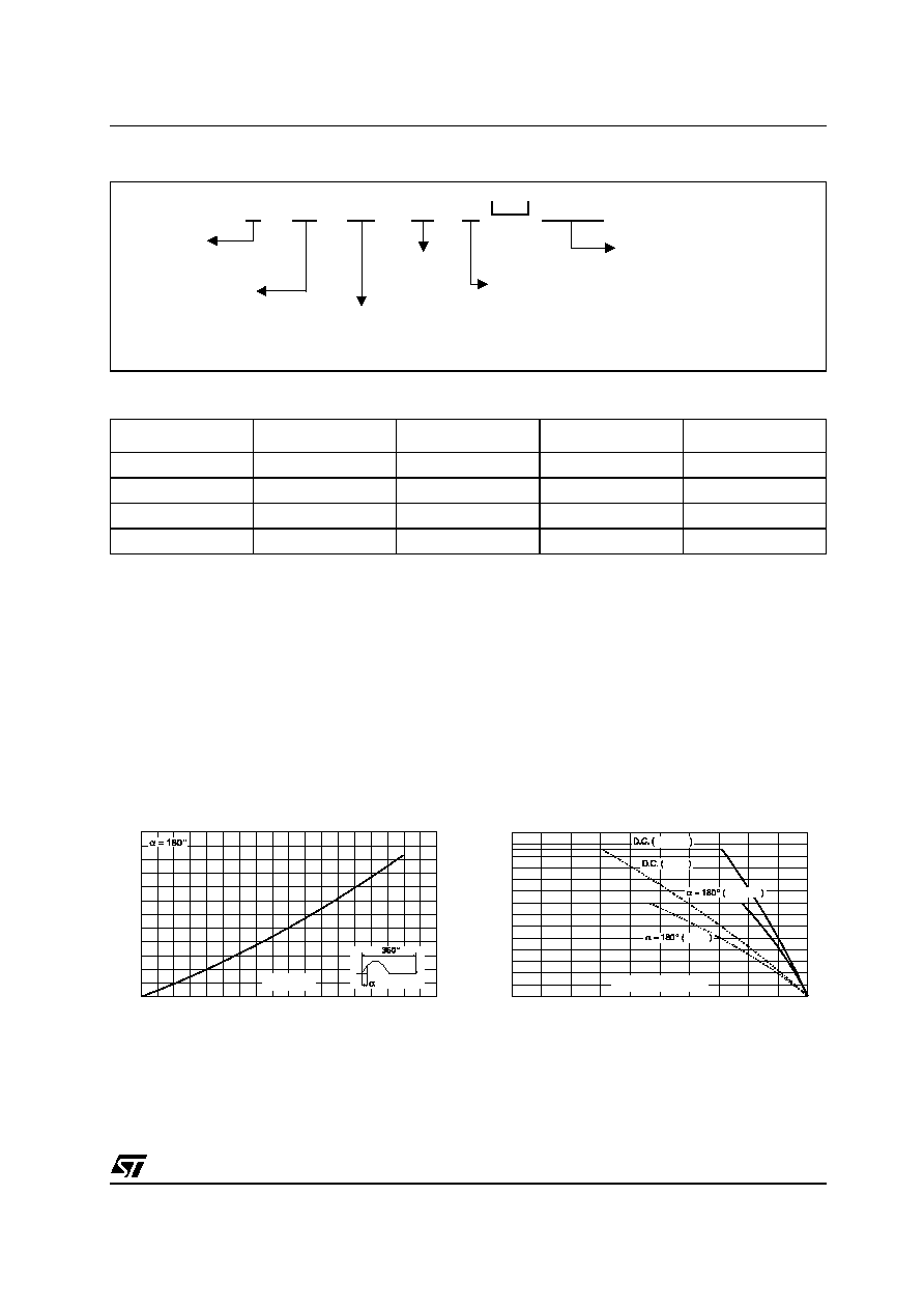
Fig. 1: Maximum average power dissipation
versus average on-state current.
Fig. 2-1: Average and D.C. on-state current
versus lead temperature (SOT-223/TO-92).
X 02 02 M A 1BA2
Blank
SENSITIVE
SCR
SERIES
CURRENT: 1.25A
SENSITIVITY:
02: 200µA
05: 50µA
VOLTAGE:
M: 600V
N: 800V
PACKAGE:
A: TO-92
N: SOT-223
PACKING MODE:
1BA2: TO-92 Bulk
2BL2: TO-92 Ammopack
5BA4: SOT-223 Tape & Reel
P(W)
1.2
1.0
0.8
0.6
0.4
0.2
0.0
0.0
0.1
0.2
0.3
0.4
0.5
0.6
0.7
0.8
0.9
IT(av)(A)
SOT-223
SOT-223
TO-92
TO-92
IT(av)(A)
0.8
1.4
1.2
1.0
0.6
0.4
0.2
0.0
0
25
50
75
100
125
Tlead or Tlab(∞C)
X02 Series
4/6
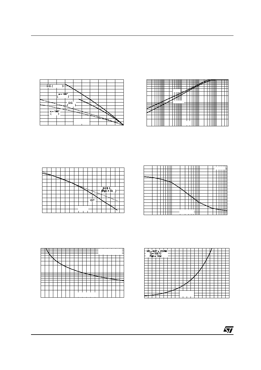
Fig. 2-2: Average and D.C. on-state current
versus ambient temperature (device mounted on
FR4 with recommended pad layout) (SOT-223/
TO-92).
Fig. 3: Relative variation of thermal impedance
junction to ambient versus pulse duration
(SOT-223/TO-92).
Fig. 4: Relative variation of gate trigger current,
holding current and latching current versus
junction temperature (typical values).
Fig. 5: Relative variation of holding current
versus gate-cathode resistance (typical values).
Fig. 6: Relative variation of dV/dt immunity
versus gate-cathode resistance (typical values).
Fig. 7: Relative variation of dV/dt immunity
versus gate-cathode capacitance (typical values).
SOT-223
SOT-223
TO-92
TO-92
IT(av)(A)
0
25
50
75
100
125
0.8
1.4
1.2
1.0
0.6
0.4
0.2
0.0
Tamb(∞C)
1E-2
1E-1
1E+0
1E+1
1E+2
5E+2
0.01
0.10
1.00
K = [Zth(j-a)/Rth(j-a)]
tp(s)
SOT-223
TO-92
IGT, IH, IL[Tj]/IGT, IH, IL[Tj] = 25∞C]
1.50
1.25
1.00
0.75
0.50
0.25
0.00
-40
-20
0
20
40
60
80
100
120 140
Tj(∞C)
1E-2
1E-1
1E+0
1E+1
0.0
0.5
1.0
1.5
2.0
2.5
3.0
3.5
4.0
IH[Rgk] / IH[Rgk = 1 k
]
Tj = 25∞C
Rgk(k
)
0.0
0.2
0.4
0.6
0.8
1.0
1.2
1.4
1.6
1.8
2.0
0.1
1.0
10.0
Tj = 125∞C
VD = 0.67xVDRM
dV/dt[Rgk]/dV/dt [Rgk=1k
]
Rgk(k
)
dV/dt[Cgk] / dV/dt[Rgk = 1k ]
20
18
16
14
12
10
8
6
4
2
0
0
2
4
6
8
10
12
14
16
18
20
22
Cgk(nF)
X02 Series
5/6
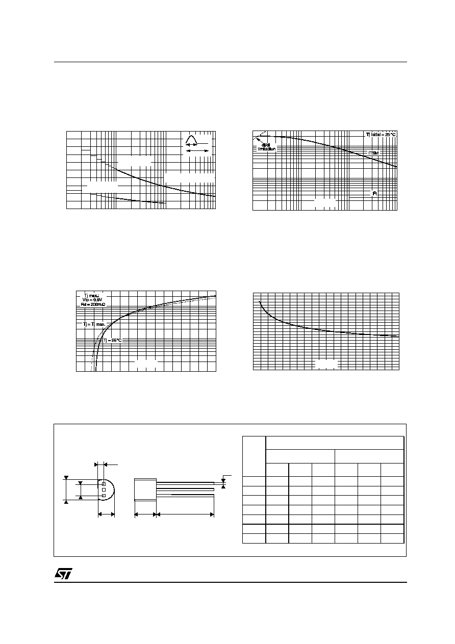
Fig. 8: Surge peak on-state current versus
number of cycles.
Fig. 9: Non-repetitive surge peak on-state
current for a sinusoidal pulse with width
tp < 10 ms, and corresponding value of I≤t.
Fig. 10: On-state characteristics (maximum
values).
Fig. 11: Thermal resistance junction to ambient
versus copper surface under tab (Epoxy printed
circuit board FR4, copper thickness: 35
µ
m)
(SOT-223).
1
10
100
1000
0
5
10
15
20
25
ITSM(A)
Nonrepetitive
Tjinitial=25∞C
Repetitive
Tamb=25∞C
Onecycle
tp=10ms
Number of cycles
ITSM(A), I t(A S)
2
2
1.00
10.00
0.10
0.01
300
100
10
1
tp(ms)
ITM(A)
VTM(V)
3E+1
1E+1
1E+0
1E-1
2.0
2.5
3.0
3.5
4.0
4.5
1.5
1.0
0.5
Rth(j-a) (∞C/W)
S(cm )
2
4.0
4.5
5.0
3.5
3.0
2.5
2.0
1.5
1.0
0.5
0.0
130
120
110
100
90
80
70
60
50
40
30
20
10
0
PACKAGE MECHANICAL DATA
TO-92 (Plastic)
D
F
a
E
B
A
C
REF.
DIMENSIONS
Millimeters
Inches
Min.
Typ.
Max.
Min.
Typ.
Max.
A
1.35
0.053
B
4.70
0.185
C
2.54
0.100
D
4.40
0.173
E
12.70
0.500
F
3.70
0.146
a
0.50
0.019