 | –≠–ª–µ–∫—Ç—Ä–æ–Ω–Ω—ã–π –∫–æ–º–ø–æ–Ω–µ–Ω—Ç: Z0109SA | –°–∫–∞—á–∞—Ç—å:  PDF PDF  ZIP ZIP |
Æ
1/8
Table 1: Main Features
DESCRIPTION
The Z01 series is suitable for general purpose AC
switching applications. They can be found in appli-
cations such as home appliances (electrovalve,
pump, door lock, small lamp control), fan speed
controllers,...
Different gate current sensitivities are available, al-
lowing optimized performances when controlled
directly from microcontrollers.
Symbol
Value
Unit
I
T(RMS)
1
A
V
DRM
/V
RRM
600 to 800
V
I
GT (Q
1
)
3 to 25
mA
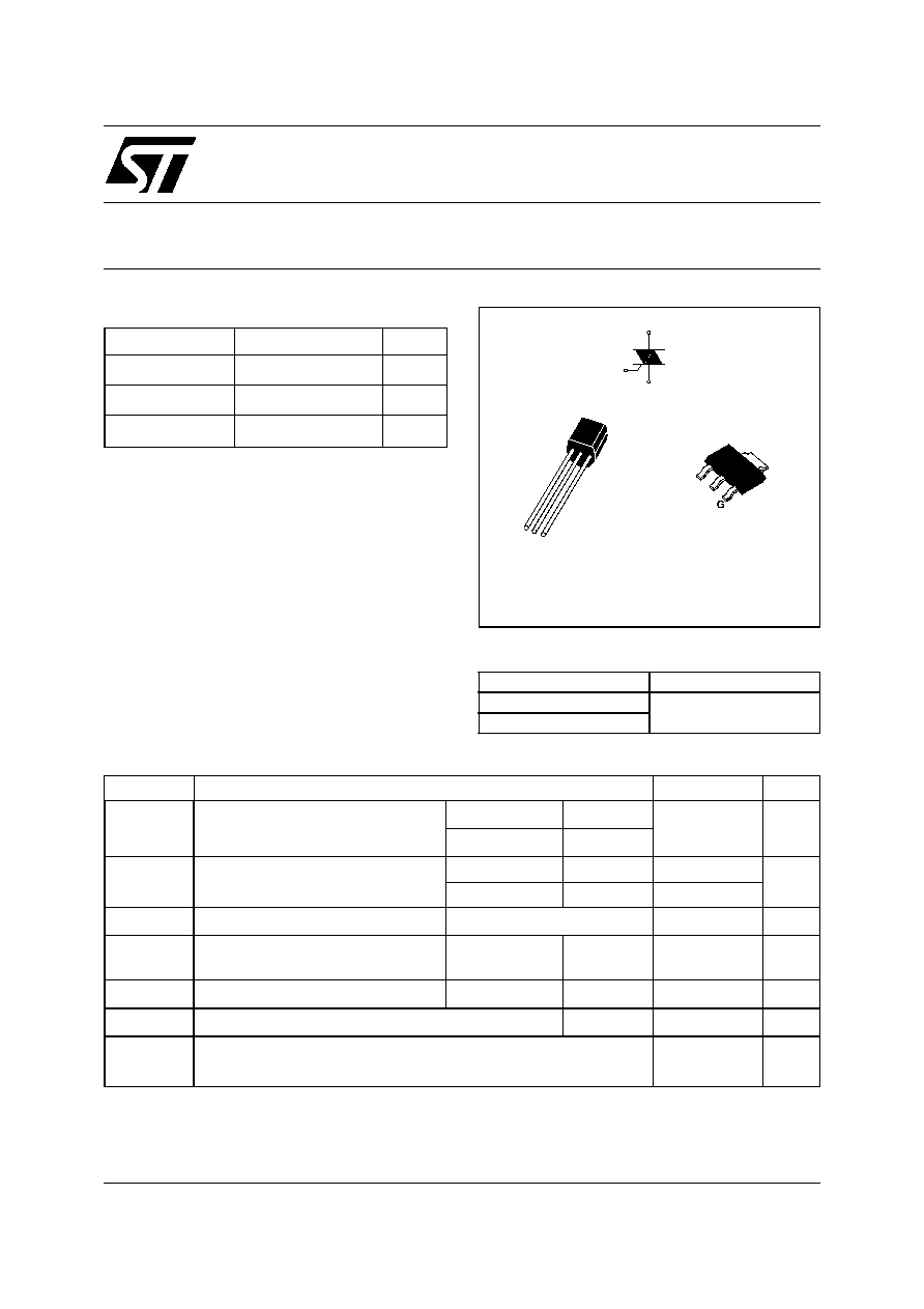
Z01
1A TRIAC
S
REV. 5
February 2005
STANDARD
Table 2: Order Codes
Part Number
Marking
Z01xxA
See page table 8 on
page 7
Z01xxN
TO-92
(Z01xxA)
SOT-223
(Z01xxN)
A2
A1
G
G A2
A1
A2
A1
A2
Table 3: Absolute Maximum Ratings
Symbol
Parameter
Value
Unit
I
T(RMS)
RMS on-state current
(full sine wave)
SOT-223
T
tab
= 90∞C
1
A
TO-92
T
L
= 50∞C
I
TSM
Non repetitive surge peak on-state
current (full cycle, T
j
initial = 25∞C)
F = 50 Hz
t = 20 ms
8
A
F = 60 Hz
t = 16.7 ms
8.5
I
≤
t
I
≤
t Value for fusing
t
p
= 10 ms
0.35
A
≤
s
dI/dt
Critical rate of rise of on-state cur-
rent I
G
= 2 x I
GT
, t
r
100 ns
F = 120 Hz
T
j
= 125∞C
20
A/µs
I
GM
Peak gate current
t
p
= 20 µs
T
j
= 125∞C
1
A
P
G(AV)
Average gate power dissipation
T
j
= 125∞C
1
W
T
stg
T
j
Storage junction temperature range
Operating junction temperature range
- 40 to + 150
- 40 to + 125
∞C
Z01
2/8
Tables 4: Electrical Characteristics (T
j
= 25∞C, unless otherwise specified)
Table 5: Static Characteristics
Table 6: Thermal resistances
Symbol
Test Conditions
Quadrant
Z01
Unit
03
07
09
10
I
GT
(1)
V
D
= 12 V R
L
= 30
I - II - III - IV MAX.
3
5
5
7
10
10
25
25
mA
V
GT
ALL
MAX.
1.3
V
V
GD
V
D
= V
DRM
R
L
= 3.3 k
T
j
= 125∞C
ALL
MIN.
0.2
V
I
H
(2)
I
T
= 50 mA
MAX.
7
10
10
25
mA
I
L
I
G
= 1.2 I
GT
I - III - IV
MAX.
7
10
15
25
mA
II
15
20
25
50
dV/dt (2)
V
D
= 67 %V
DRM
gate open T
j
= 110∞C
MIN.
10
20
50
100
V/µs
(dI/dt)c (2) (dV/dt)c = 0.44 A/ms T
j
= 110∞C
MIN.
0.5
1
2
5
A/ms
Symbol
Test Conditions
Value
Unit
V
TM
(2)
I
TM
= 1.4 A t
p
= 380 µs
T
j
= 25∞C
MAX.
1.56
V
V
to
(2)
Threshold voltage
T
j
= 125∞C
MAX.
0.95
V
R
d
(2)
Dynamic resistance
T
j
= 125∞C
MAX.
400
m
I
DRM
I
RRM
V
DRM
= V
RRM
T
j
= 25∞C
MAX.
5
µA
T
j
= 125∞C
0.5
mA
Note 1: minimum IGT is guaranted at 5% of IGT max.
Note 2: for both polarities of A2 referenced to A1.
Symbol
Parameter
Value
Unit
R
th(j-t)
Junction to tab (AC)
SOT-223
25
∞C/W
R
th(j-I)
Junction to lead (AC)
TO-92
60
R
th(j-a)
Junction to ambient
S = 5 cm
≤
SOT-223
60
∞C/W
TO-92
150
S = Copper surface under tab.
Z01
3/8
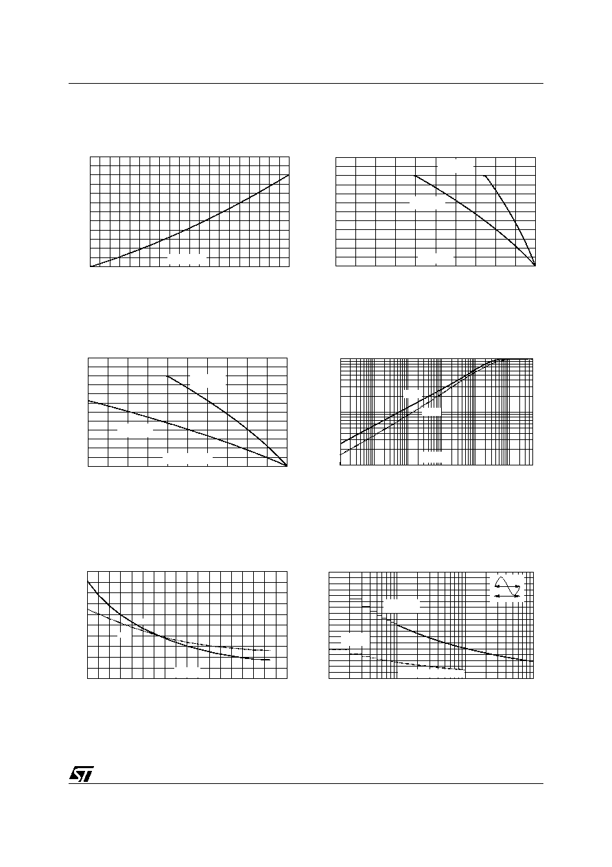
Figure 1: Maximum power dissipation versus
RMS on-state current (full cycle)
Figure 2: RMS on-state current versus case
temperature (full cycle)
Figure 3: RMS on-state current versus ambient
temperature (full cycle)
Figure 4: Relative variation of thermal
impedance versus pulse duration
Figure 5: Relative variation of gate trigger
current, holding current and latching current
versus junction temperature (typical values)
Figure 6: Surge peak on-state current versus
number of cycles
P(W)
0.0
0.1
0.2
0.3
0.4
0.5
0.6
0.7
0.8
0.9
1.0
0.00
0.25
0.50
0.75
1.00
1.25
1.50
I
(A)
T(RMS)
0
25
50
75
100
125
0.0
0.2
0.4
0.6
0.8
1.0
1.2
I
(A)
T(RMS)
R
=
(SOT-223)
th(j-a)
R
th(j-t)
R
=
(TO-92)
th(j-a)
R
th(j-l)
T
(∞C)
amb
I
(A)
T(RMS)
0
25
50
75
100
125
0.0
0.2
0.4
0.6
0.8
1.0
1.2
R
= 60∞C/W
(SOT-223)
th(j-a)
R
= 150∞C/W
(TO-92)
th(j-a)
T or
(∞C)
l
T
tab
K=[Z
/R
th(j-a)
th(j-a)]
1E-3
1E-2
1E-1
1E+0
1E+1
1E+2
5E+2
0.01
0.10
1.00
t (s)
p
Z01xxA
Z01xxN
-40
-20
0
20
40
60
80
100
120
140
0.0
0.5
1.0
1.5
2.0
2.5
I
, I , I [T ] /
GT
H
L
j
I
, I , I [T =25∞C]
GT
H
L
j
T (∞C)
j
I
GT
I
H
& I
L
1
10
100
1000
0
1
2
3
4
5
6
7
8
9
One cycle
t=20ms
I
(A)
TSM
Number of cycles
Non repetitive
T initial = 25∞C
j
Repetitive
T
= 25∞C
amb
Z01
4/8
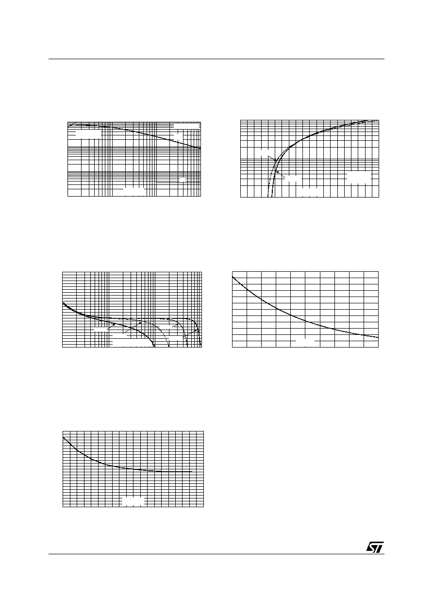
Figure 7: Non-repetitive surge peak on-state
current for a sinusoidal pulse with width t
p
< 10 ms
and corresponding value of I
2
t
Figure 8: On-state characteristics (maximum
values)
Figure 9: Relative variation of critical rate of
decrease of main current versus (dV/dt)c
(typical values)
Figure 10: Relative variation of critical rate of
decrease of main current versus junction
temperature
Figure 11: SOT-223 Thermal resistance junction
to ambient versus copper surface under tab
(printed circuit board FR4, copper thickness:
35 µm)
0.01
0.10
1.00
10.00
0.1
1.0
10.0
100.0
t (ms)
p
I
(A), I t (A s)
TSM
2
2
I t
2
dI/dt limitation:
20A/µs
T initial = 25∞C
j
I
TSM
I
(A)
TM
0.0
0.5
1.0
1.5
2.0
2.5
3.0
3.5
4.0
4.5
5.0
0.1
1.0
10.0
V
(V)
TM
T =
max.
j
T
j
T = 25∞C
j
T =max.
j
V =0.95 V
R =420 m
t0
d
0.1
1.0
10.0
100.0
0.0
0.2
0.4
0.6
0.8
1.0
1.2
1.4
1.6
1.8
2.0
2.2
2.4
2.6
Z0103
Z0107
Z0110
Z0109
(dI/dt)c [(dV/dt)c] / Specified (dI/dt)c
(dV/dt)c (V/µs)
0
25
50
75
100
125
0
1
2
3
4
5
6
(dI/dt)c [T ] /
Specified]
j
(dI/dt)c [T
j
T (∞C)
j
R
(∞C/W)
th(j-a)
0.0
0.5
1.0
1.5
2.0
2.5
3.0
3.5
4.0
4.5
5.0
0
10
20
30
40
50
60
70
80
90
100
110
120
130
S(cm≤)
Z01
5/8
Figure 12: Ordering Information Scheme
Table 7: Product Selector
Part Number
Voltage
Sensitivity
Type
Package
600 V
700 V
800 V
Z0103MA
X
3 mA
Standard
TO-92
Z0103MN
X
3 mA
Standard
SOT-223
Z0103SA
X
3 mA
Standard
TO-92
Z0103SN
X
3 mA
Standard
SOT-223
Z0103NA
X
3 mA
Standard
TO-92
Z0103NN
X
3 mA
Standard
SOT-223
Z0107MA
X
5 mA
Standard
TO-92
Z0107MN
X
5 mA
Standard
SOT-223
Z0107SA
X
5 mA
Standard
TO-92
Z0107SN
X
5 mA
Standard
SOT-223
Z0107NA
X
5 mA
Standard
TO-92
Z0107NN
X
5 mA
Standard
SOT-223
Z0109MA
X
10 mA
Standard
TO-92
Z0109MN
X
10 mA
Standard
SOT-223
Z0109SA
X
10 mA
Standard
TO-92
Z0109SN
X
10 mA
Standard
SOT-223
Z0109NA
X
10 mA
Standard
TO-92
Z0109NN
X
10 mA
Standard
SOT-223
Z0110MA
X
25 mA
Standard
TO-92
Z0110MN
X
25 mA
Standard
SOT-223
Z0110SA
X
25 mA
Standard
TO-92
Z0110SN
X
25 mA
Standard
SOT-223
Z0110NA
X
25 mA
Standard
TO-92
Z0110NN
X
25 mA
Standard
SOT-223
Z 01 03 M A
1AA2
[BLANK]
Triac series
Current
Sensitivity
Voltage
Package
Packing mode
01 = 1A
03 = 3mA
07 = 5mA
09 = 10mA
10 = 25mA
M = 600V
S = 700V
N = 800V
A = TO-92
N = SOT-223
1AA2 = TO-92 Bulk (preferred)
2AL2 = TO-92 Ammopack
5AL2 = TO-92 Tape & reel
5AA4 = SOT-223 Tape & reel