1/3
January 2002
PSD3XX ZPSD3XX ZPSD3XXV
PSD3XXR ZPSD3XXR ZPSD3XXRV
Low Cost Field Programmable Microcontroller Peripherals
FEATURES SUMMARY
s
Single Supply Voltage:
≠ 5 V±10% for PSD3xx, ZPSD3xx, PSD3xxR,
ZPSD3xxR
≠ 2.7 to 5.5 V for ZPSD3xxV, ZPSD3xxRV
s
Up to 1 Mbit of EPROM
s
Up to 16 Kbit SRAM
s
Input Latches
s
Programmable I/O ports
s
Page Logic
s
Programmable Security
Figure 1. Packages
PLDCC44 (J)
CLDCC44 (L)
PQFP44 (M)
TQFP44 (U)

i
PSD3XX Family
PSD3XX ZPSD3XX ZPSD3XXV
PSD3XXR ZPSD3XXR ZPSD3XXRV
Low Cost Microcontroller Peripherals
Table of Contents
1
Introduction ...........................................................................................................................................................1
2
Notation ................................................................................................................................................................2
3
Key Features ........................................................................................................................................................4
4
PSD3XX Family Feature Summary ......................................................................................................................5
5
Partial Listing of Microcontrollers Supported ........................................................................................................6
6
Applications ..........................................................................................................................................................6
7
ZPSD Background ................................................................................................................................................6
7.1
Integrated Power Management
TM
Operation .............................................................................................7
8
Operating Modes (MCU Configurations) ............................................................................................................10
9
Programmable Address Decoder (PAD).............................................................................................................12
10
I/O Port Functions ...............................................................................................................................................15
10.1
CSIOPORT Registers..............................................................................................................................15
10.2
Port A (PA0-PA7).....................................................................................................................................16
10.2.1 Port A (PA0-PA7) in Multiplexed Address/Data Mode................................................................16
10.2.2 Port A (PA0-PA7) in Non-Multiplexed Address/Data Mode ........................................................17
10.3
Port B (PB0-PB7).....................................................................................................................................18
10.3.1 Port B (PA0-PA7) in Multiplexed Address/Data Mode................................................................18
10.3.2 Port B (PA0-PA7) in Non-Multiplexed Address/Data Mode ........................................................19
10.4
Port C (PC0-PC2) ....................................................................................................................................20
10.5
ALE/AS Input Pin .....................................................................................................................................20
11
PSD Memory ......................................................................................................................................................21
11.1
EPROM....................................................................................................................................................21
11.2
SRAM (Optional)......................................................................................................................................21
11.3
Page Register (Optional) .........................................................................................................................21
11.4
Programming and Erasure.......................................................................................................................21
12
Control Signals ...................................................................................................................................................22
12.1
ALE or AS ................................................................................................................................................22
12.2
WR or R/W...............................................................................................................................................22
12.3
RD/E/DS (DS option not available on 3X1 devices) ................................................................................22
12.4
PSEN or PSEN ........................................................................................................................................22
12.5
A19/CSI ...................................................................................................................................................23
12.6
Reset Input ..............................................................................................................................................24
13
Program/Data Space and the 8031 ....................................................................................................................26
14
Systems Applications..........................................................................................................................................27
15
Security Mode .....................................................................................................................................................30
16
Power Management............................................................................................................................................30
16.1
CSI Input..................................................................................................................................................30
16.2
CMiser Bit ................................................................................................................................................30
16.3
Turbo Bit (ZPSD Only).............................................................................................................................31
16.4
Number of Product Terms in the PAD Logic............................................................................................31
16.5
Composite Frequency of the Input Signals to the PAD Logic..................................................................32
16.6
Loading on I/O Pins .................................................................................................................................33
17
Calculating Power ...............................................................................................................................................34

ii
PSD3XX Family
PSD3XX ZPSD3XX ZPSD3XXV
PSD3XXR ZPSD3XXR ZPSD3XXRV
Low Cost Microcontroller Peripherals
Table of Contents
(cont.)
18
Specifications......................................................................................................................................................37
18.1
Absolute Maximum Ratings .....................................................................................................................37
18.2
Operating Range .....................................................................................................................................37
18.3
Recommended Operating Conditions......................................................................................................37
18.4
Pin Capacitance.......................................................................................................................................37
18.5
AC/DC Characteristics ≠ PSD3XX/ZPSD3XX (All 5 V devices) ..............................................................38
18.6
AC/DC Characteristics ≠ PSD3XXV (3 V devices only)...........................................................................39
18.7
Timing Parameters ≠ PSD3XX/ZPSD3XX (All 5 V devices)....................................................................40
18.8
Timing Parameters ≠ ZPSD3XXV (3 V devices only) ..............................................................................42
18.9
Timing Diagrams for PSD3XX Parts.......................................................................................................44
18.10 AC Testing ...............................................................................................................................................65
19
Pin Assignments .................................................................................................................................................66
20
Package Information ...........................................................................................................................................67
21
Package Drawings ..............................................................................................................................................68
22
PSD3XX Product Ordering Information ..............................................................................................................72
22.1
PSD3XX Selector Guide..........................................................................................................................72
22.2
Part Number Construction .......................................................................................................................73
22.3
Ordering Information................................................................................................................................73
23
Data Sheet Revision History ...............................................................................................................................80
1
1.0
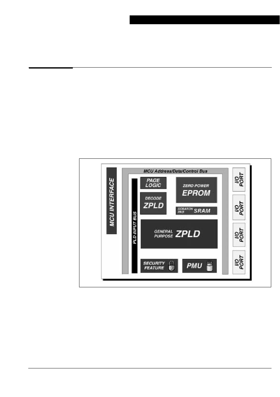
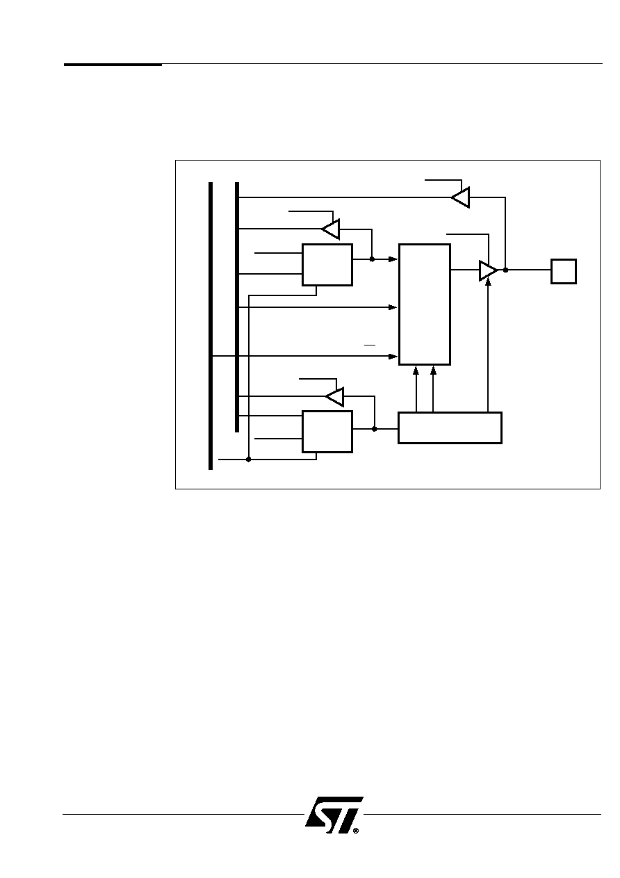
Introduction
Programmable Peripheral
PSD3XX Family
Field-Programmable Microcontroller Peripheral
The low cost PSD3XX family integrates high-performance and user-configurable blocks of
EPROM, programmable logic, and optional SRAM into one part. The PSD3XX products
also provide a powerful microcontroller interface that eliminates the need for external
"glue logic". The part's integration, small form factor, low power consumption, and ease of
use make it the ideal part for interfacing to virtually any microcontroller.
The major functional blocks of the PSD3XX include:
∑
Two programmable logic arrays
∑
256Kb to 1 Mb of EPROM
∑
Optional 16 Kb SRAM
∑
Input latches
∑
Programmable I/O ports
∑
Page logic
∑
Programmable security.
The PSD3XX family architecture (Figure 1) can efficiently interface with, and enhance,
almost any 8- or 16-bit microcontroller system. This solution provides microcontrollers the
following:
∑
Chip-select logic, control logic, and latched address signals that are otherwise
implemented discretely
∑
Port expansion (reconstructs lost microcontroller I/O)
∑
Expanded microcontroller address space (up to 16 times)
∑
An EPROM (with security) and optional SRAM
∑
Compatible with 8031-type architectures that use separate Program and Data Space
∑
Interface to shared external resources.

PSD3XX Family
2
2.
Notation
For a complete product comparison, refer to Table 1.
PSD3XX references the standard version of the PSD3XX family, which are ideal for
general-purpose embedded control applications.
PSD3XXR SRAM-less version of the PSD3XX. If you don't require the 16 Kb SRAM or
need a larger external SRAM, go with this part to save cost.
ZPSD3XX has improved technology that helps reduce current consumption using the Turbo
bit. Excellent if you require a 5 V version of the PSD3XX that uses less power.
ZPSD3XXR SRAM-less version of the ZPSD3XX.
ZPSD3XXV 2.7 V to 5.5 V operation, ideal for very low-power and low-voltage
applications.
ZPSD3XXRV SRAM-less version of the ZPSD3XXV.
Throughout this data sheet, references are made to the PSD3XX. In most cases, these
references also cover the entire family. Exceptions will be noted. References, such as
"3X1 only" cover all parts that have a 301 or 311 in the part number. Use the following table
to determine what references cover which product versions:
Reference
PSD3XX
PSD3XXR
ZPSD3XX
ZPSD3XXR
ZPSD3XXV
ZPSD3XXRV
PSD3XX
X
X
X
X
X
X
PSD
PSD3XX only
X
X
Non-ZPSD
X
X
ZPSD only
ZPSD3XX
X
X
X
X
Non-V versions
X
X
X
X
V versions only
V suffix
X
X
ZPSD3XXV only
SRAM-less
X
X
X
Non-R
The PSD3XX I/O ports can be used for:
∑
Standard I/O ports
∑
Programmable chip select outputs
∑
Address inputs
∑
Demultiplexed address outputs
∑
A data bus port for non-multiplexed MCU applications
∑
A data bus "repeater" port that shares and arbitrates the local MCU data bus with
external devices.
Implementing your design has never been easier than with PSDsoft --ST's software
development suite. Using PSDsoft, you can do the following:
∑
Configure your PSD3XX to work with virtually any microcontroller
∑
Specify what you want implemented in the programmable logic using a high-level
Hardware Description Language (HDL)
∑
Simulate your design
∑
Download your design to the part using a programmer.
1.0
Introduction
(cont.)
PSD3XX Family
3
PROG.
PORT
EXP.
PORT
C
PC0≠
PC2
ES0
ES1
ES2
ES3
ES4
ES5
ES6
ES7
PROG.
CONTROL
SIGNALS
A19/CSI
RESET
WR/R/W
RD/E/DS
ALE/AS
BHE/PSEN
PAD A
RESET
WR
ALE/AS
RD
PAD B
A11≠A15
PROG.
PORT
EXP.
PORT
B
PB0≠
PB7
PROG.
PORT
EXP.
PORT
A
PA0≠
PA7
A19/CSI
RESET
ALE/AS
A19/CSI
A8≠A10
WR
RD
ALE/AS
L
A
T
C
H
L
A
T
C
H
AD8≠AD15
AD0≠AD7
D8≠D15
13 P.T.
27 P.T.
OPTIONAL
PAGE LOGIC
*
LOGIC IN
EPROM
256Kb TO 1Mb
A16≠A18
CS8≠
CS10
CS0≠
CS7
OPTIONAL
SRAM
16K BIT
**
D0≠D7
RS0
A0≠A7
AD0≠AD7/D0≠D7
D8≠D15
CSIOPORT
PROG. CHIP
CONFIGURATION
X8, X16
MUX or NON≠MUX BUSSES
SECURITY MODE
16/8
MUX
CSIOPORT
TRACK MODE
SELECTS
P3≠P0
Figure 1.
PSD3XX
Family
Architecture
*
*
Not available for 3X1 devices.
**
SRAM not available on "R" versions.

PSD3XX Family
4
3.0
Key Features
t
Single-chip programmable peripheral for microcontroller-based applications
t
256K to 1 Mbit of UV EPROM with the following features:
∑
Configurable as 32, 64, or 128 K x 8; or as 16, 32, or 64 K x 16
∑
Divided into eight equally-sized mappable blocks for optimized address mapping
∑
As fast as 70 ns access time, which includes address decoding
t
Optional 16 Kbit SRAM is configurable as 2K x 8 or 1K x 16. The access time can be
as quick as 70 ns, including address decoding.
t
19 I/O pins that can be individually configured for :
∑
Microcontroller I/O port expansion
∑
Programmable Address decoder (PAD) I/O
∑
Latched address output
∑
Open-drain or CMOS output
t
Two Programmable Arrays (PAD A and PAD B) replace your PLD or decoder, and have
the following features:
∑
Up to 18 Inputs and 24 outputs
∑
40 Product terms (13 for PAD A and 27 for PAD B)
∑
Ability to decode up to 1 MB of address without paging
t
Microcontroller logic that eliminates the need for external "glue logic" has the following
features:
∑
Ability to interface to multiplexed and non-multiplexed buses
∑
Built-in address latches for multiplexed address/data bus
∑
ALE and Reset polarity are programmable (Reset polarity not programmable on
V-versions)
∑
Multiple configurations are possible for interface to many different microcontrollers
t
Optional built-in page logic expands the MCU address space by up to 16 times
t
Programmable power management with standby current as low as 1µA for low-voltage
version
∑
CMiser bit --programmable option to reduce AC power consumption in memory
∑
Turbo Bit (ZPSD only)--programmable bit to reduce AC and DC power consumption
in the PADs.
t
Track Mode that allows other microcontrollers or host processors to share access to the
local data bus
t
Built-in security locks the device and PAD decoding configuration
t
Wide Operating Voltage Range
∑
V-versions: 2.7 to 5.5 volts
∑
Others: 4.5 to 5.5 volts
t
Available in a variety of packaging (44-pin PLDCC, CLDCC, TQFP, and PQFP)
t
Simple, menu-driven software (PSDsoft) allows configuration and design entry on a PC.
PSD3XX Family
5
Use the following table to determine which PSD product will fit your needs. Refer back to
this page whenever there is confusion as to which part has what features.
4.0
PSD3XX Family
Feature
Summary
Typical
# PLD
EPROM
SRAM
Page
Turbo
Bus
Standby
Part
Inputs
Size
Size
Reg
Voltage
Bit
Width
Current
PSD301R
14
256 Kb
5 V
x8 or x16
50 µA
PSD311R
14
256 Kb
5 V
x8
50 µA
PSD302R
18
512 Kb
X
5 V
x8 or x16
50 µA
PSD312R
18
512 Kb
X
5 V
x8
50 µA
PSD303R
18
1 Mb
X
5 V
x8 or x16
50 µA
PSD313R
18
1 Mb
X
5 V
x8
50 µA
ZPSD301R
14
256 Kb
5 V
X
x8 or x16
10 µA
ZPSD311R
14
256 Kb
5 V
X
x8
10 µA
ZPSD302R
18
512 Kb
X
5 V
X
x8 or x16
10 µA
ZPSD312R
18
512 Kb
X
5 V
X
x8
10 µA
ZPSD303R
18
1 Mb
X
5 V
X
x8 or x16
10 µA
ZPSD313R
18
1 Mb
X
5 V
X
x8
10 µA
PSD301
14
256 Kb
16 Kb
5 V
x8 or x16
50 µA
PSD311
14
256 Kb
16 Kb
5 V
x8
50 µA
PSD302
18
512 Kb
16 Kb
X
5 V
x8 or x16
50 µA
PSD312
18
512 Kb
16 Kb
X
5 V
x8
50 µA
PSD303
18
1 Mb
16 Kb
X
5 V
x8 or x16
50 µA
PSD313
18
1 Mb
16 Kb
X
5 V
x8
50 µA
ZPSD301
14
256 Kb
16 Kb
5 V
X
x8 or x16
10 µA
ZPSD311
14
256 Kb
16 Kb
5 V
X
x8
10 µA
ZPSD302
18
512 Kb
16 Kb
X
5 V
X
x8 or x16
10 µA
ZPSD312
18
512 Kb
16 Kb
X
5 V
X
x8
10 µA
ZPSD303
18
1 Mb
16 Kb
X
5 V
X
x8 or x16
10 µA
ZPSD313
18
1 Mb
16 Kb
X
5 V
X
x8
10 µA
ZPSD301V
1
14
256 Kb
16 Kb
2.7 V
X
x8 or x16
1 µA
ZPSD311V
1
14
256 Kb
16 Kb
2.7 V
X
x8
1 µA
ZPSD302V
1
18
512 Kb
16 Kb
X
2.7 V
X
x8 or x16
1 µA
ZPSD312V
1
18
512 Kb
16 Kb
X
2.7 V
X
x8
1 µA
ZPSD303V
1
18
1 Mb
16 Kb
X
2.7 V
X
x8 or x16
1 µA
ZPSD313V
1
18
1 Mb
16 Kb
X
2.7 V
X
x8
1 µA
NOTES: 1. Low power versions of the ZPSD3XX (ZPSD3XXV) can only accept an active-low level Reset input.

5.0
Partial Listing
of
Microcontrollers
Supported
PSD3XX Family
6
t
Motorola family: 68HC11, 68HC16, M68000/10/20, M68008, M683XX, 68HC05C0
t
Intel family: 80C31, 80C51, 80C196/198, 80C186/188
t
Philips family: 80C31 and 80C51 based MCUs
t
Zilog: Z8, Z80, Z180
t
National: HPC16000, HPC46400
t
Echelon/Motorola/Toshiba: NEURON
Æ
3150
TM
Chip
6.0
Applications
t
Telecommunications:
∑
Cellular phone
∑
Digital PBX
∑
Digital speech
∑
FAX
∑
Digital Signal Processing (DSP)
t
Portable Industrial Equipment:
∑
Industrial control
∑
Measurement meters
∑
Data recorders
t
Instrumentation
t
Medical Instrumentation:
∑
Hearing aids
∑
Monitoring equipment
∑
Diagnostic tools
t
Computers--notebooks, portable PCs, and palm-top computers:
∑
Peripheral control (fixed disks, laser printers, etc.)
∑
Modem Interface
∑
MCU peripheral interface
Portable and battery-powered systems have recently become major embedded control
application segments. As a result, the demand for electronic components having extremely
low power consumption has increased dramatically. Recognizing this trend, ST
developed a new lower power 3XX part, denoted ZPSD3XX. The Z stands for Zero-power
because ZPSD products virtually eliminate the DC component of power consumption,
reducing it to standby levels. Virtual elimination of the DC component is the basis for the
words "Zero-power" in the ZPSD name. ZPSD products also minimize the AC power
component when the chip is changing states. The result is a programmable microcontroller
peripheral family that replaces discrete circuit components, while drawing less power.
7.0
ZPSD
Background
PSD3XX Family
7
7.0
ZPSD
Background
(cont.)
Integrated Power Management
TM
Operation
Upon each address or logic input change to the ZPSD, the device powers up from low
power standby for a short time. Then the ZPSD consumes only the necessary power to
deliver new logic or memory data to its outputs as a response to the input change. After the
new outputs are stable, the ZPSD latches them and automatically reverts back to standby
mode. The I
CC
current flowing during standby mode and during DC operation is identical
and is only a few microamperes.
The ZPSD automatically reduces its DC current drain to these low levels and does not
require controlling by the CSI (Chip Select Input). Disabling the CSI pin unconditionally
forces the ZPSD to standby mode independent of other input transitions.
The only significant power consumption in the ZPSD occurs during AC operation.
The ZPSD contains the first architecture to apply zero power techniques to memory and
logic blocks.
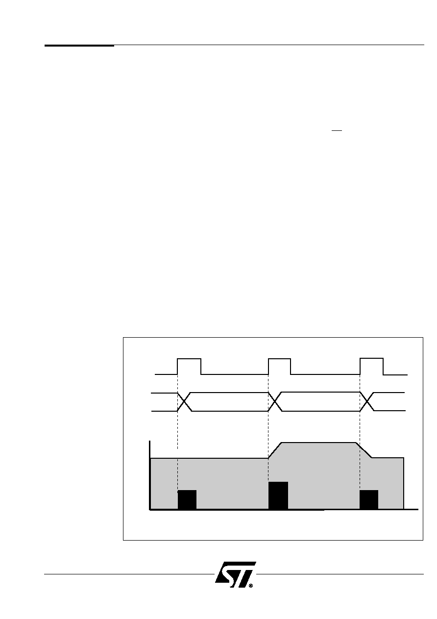
Figure 2 compares ZPSD zero power operation to the operation of a discrete solution.
A standard microcontroller (MCU) bus cycle usually starts with an ALE (or AS) pulse and
the generation of an address. The ZPSD detects the address transition and powers up for a
short time. The ZPSD then latches the outputs of the PAD, EPROM and SRAM to the new
values. After finishing these operations, the ZPSD shuts off its internal power, entering
standby mode. The time taken for the entire cycle is less than the ZPSD's "access time."
The ZPSD will stay in standby mode while its inputs are not changing between bus cycles.
In an alternate system implementation using discrete EPROM, SRAM, and other discrete
components, the system will consume operating power during the entire bus cycle. This
is because the chip select inputs on the memory devices are usually active throughout
the entire cycle. The AC power consumption of the ZPSD may be calculated using the
composite frequency of the MCU address and control signals, as well as any other logic
inputs to the ZPSD.
ALE
DISCRETE EPROM, SRAM & LOGIC
ADDRESS
EPROM
ACCESS
SRAM
ACCESS
EPROM
ACCESS
I
CC
ZPSD
ZPSD
ZPSD
TIME
Figure 2. ZPSD Power Operation vs. Discrete Implementation

PSD3XX Family
8
Name
Type
Description
When the data bus is 8 bits:
This pin is for 8031 or compatible MCUs that use PSEN to
separate program space from data space. In this case, PSEN is
BHE/
used for reads from the EPROM. Note: if your MCU does not
PSEN
I
output a PSEN signal, pull up this pin to V
CC
.
When the data bus is 16 bits:
This pin is BHE. When low, D8-D15 are read from or written to.
Note: in programming mode, this pin is pulsed between V
PP
and 0 V.
The following control signals can be connected to this port, based on
WR/V
PP
your MCU (and the way you configure the PSD in PSDsoft):
or
I
1. WR--active-low write pulse.
R/W/V
PP
2. R/W--active-high read/active-low write input.
Note: in programming mode, this pin must be tied to V
PP
.
The following control signals can be connected to this port, based on
RD/E/DS
I
your MCU (and the way you configure the PSD in PSDsoft):
1. RD--active-low read input.
2. E--E clock input.
3. DS--active-low data strobe input (3X2/3X3 devices only)
The following control signals can be connected to this port:
1. CSI--Active-low chip select input. If your MCU supports a chip
select output, and you want the PSD to save power when not
A19/CSI
I
selected, use this pin as a chip select input.
2. If you don't wish to use the CSI feature, you may use this pin as
an additional input (logic or address) to the PAD. A19 can be
latched (with ALE/AS), or a transparent logic input.
PSD3XX/ZPSD3XX:
This pin is user-programmable and can be configured to reset on a
high- or low-level input. Reset must be applied for at least 100 ns.
Reset
I
ZPSD3XXV:
This pin is not configurable, and the chip will only reset on an
active-low level input. Reset must be applied for at least 500 ns,
and no operations may take place for an additional 500 ns minimum.
(See Figure 8.)
If you use an MCU that has a multiplexed bus:
Connect ALE or AS to this pin. The polarity of this pin is configurable.
The trailing edge of ALE/AS latches all multiplexed address inputs
ALE/AS
I
(and BHE where applicable).
If you use an MCU that does not have a multiplexed bus:
If your MCU uses ALE/AS, connect the signal to this pin.
Otherwise, use this pin for a generic logic input to the PAD.
(Non-3X1 devices only.)
These pins make up Port A. These port pins are configurable, and
PA0
can have the following functions: (see Figure 5A and 5B)
PA1
1. Track AD7-AD0. This feature repeats the MCU address and data
PA2
I/O
bus on all Port A pins.
PA3
2. MCU I/O--in this mode, the direction of the pin is defined by its
PA4
direction bit, which resides in the direction register.
PA5
3. Latched address output.
PA6
4. CMOS or open-drain output.
PA7
5. If your MCU is non-multiplexed: data bus input--connect your
data bus (D0-7) to these pins. See Figure 3.
Legend:
The Type column abbreviations are: I = input only; I/O = input/output; P = power.
Table 2.
PSD3XX Pin
Descriptions

PSD3XX Family
9
Table 2.
PSD3XX Pin
Descriptions
(cont.)
Name
Type
Description
These pins make up Port B. These port pins are configurable, and
PB0
can have the following functions: (see Figure 6)
PB1
1. MCU I/O --in this mode, the direction of the pin is defined by its
PB2
direction bit, which resides in the direction register.
PB3
2. Chip select output --each of PB0-3 has four product terms
PB4
I/O
available per pin, while PB4-7 have 2 product terms each.
PB5
See Figure 4.
PB6
3. CMOS or open-drain.
PB7
4. If your MCU is non-multiplexed, and the data bus width is
16 bits: data bus input--connect your data bus (D8-D15) to these
pins. See Figure 3.
These pins make up Port C. These port pins are configurable, and
can have the following functions (see Figure 7):
1. PAD input--when configured as an input, a bit individually
PC0
becomes an address or a logic input, depending on your PSDsoft
PC1
I/O
design file. When declared as an address, the bit(s) can be latched
PC2
with ALE/AS.
2. PAD output--when configured as an output (i.e. there is an
equation written for it in your PSDsoft design file), there is one
product term available to it.
AD0/A0
If your MCU is multiplexed:
AD1/A1
These pins are the multiplexed, low-order address/data byte
AD2/A2
(AD0-AD7). As inputs, address information is latched by the ALE/AS
AD3/A3
I/O
signal and used internally by the PSD. The pins also serve as MCU
AD4/A4
data bus inputs or outputs, depending on the MCU control signals
AD5/A5
(RD, WR, etc.).
AD6/A6
If your MCU is non-multiplexed:
AD7/A7
These pins are the low-order address inputs (A0-A7)
AD8/A8
If your MCU is multiplexed with a 16-bit data bus:
AD9/A9
These pins are the multiplexed, high-order address/data byte
AD10/A10
(AD8-AD15). As inputs, address information is latched by the
AD11/A11
I/O
ALE/AS signal and used internally the PSD. The pins also
AD12/A12
serve as MCU data bus inputs or outputs, depending on the MCU
AD13/A13
control signals (RD, WR, etc.).
AD14/A14
If your MCU is non-multiplexed or has a 8-bit data bus:
AD15/A15
These pins are the high-order address inputs (A8-A15).
GND
P
Ground Pin
V
CC
P
Supply voltage input.
Legend:
The Type column abbreviations are: I = input only; I/O = input/output; P = power.

PSD3XX Family
10
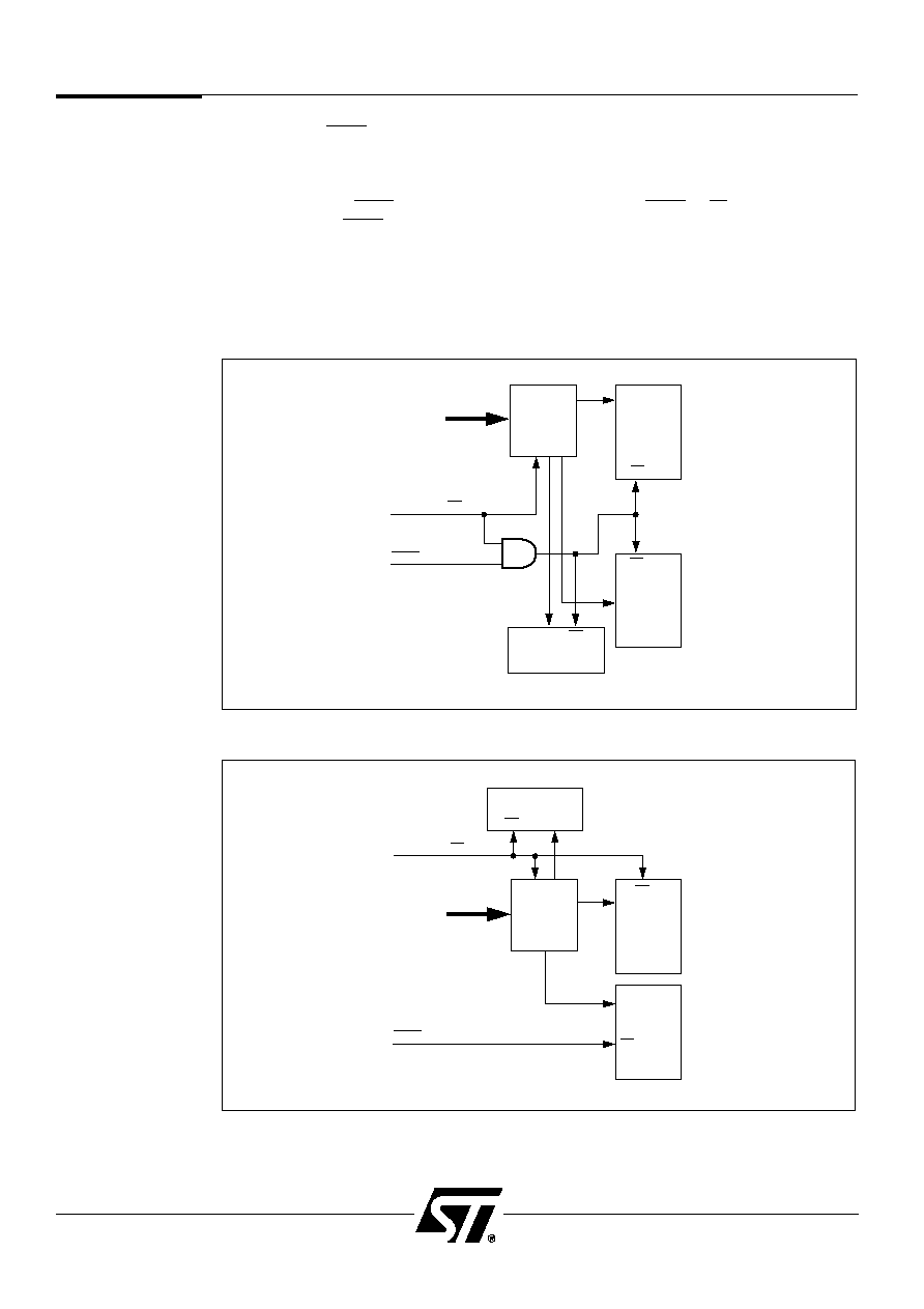
8.0
Operating
Modes (MCU
Configurations)
The PSD3XX's four operating modes enable it to interface directly to most 8- and 16-bit
microcontrollers with multiplexed and non-multiplexed address/data busses. The 16-bit
modes are not available to some devices; see Table 1. The following are the four operating
modes available:
t
Multiplexed 8-bit address/data bus
t
Multiplexed 16-bit address/data bus
t
Non-multiplexed 8-bit data bus
t
Non-multiplexed 16-bit data bus
Please read the section below that corresponds to your type of MCU. Then check the
appropriate Figure (3A/3B/3C/3D) to determine your pin connections. Table 3 lists the Port
connections in tabular form.
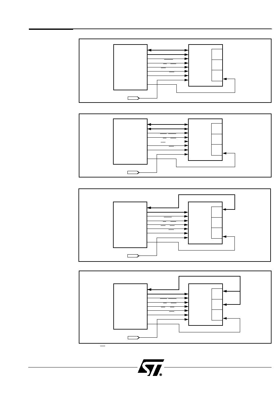
Multiplexed 8-bit address/data bus (Figure 3A)
This mode is used to interface to microcontrollers with a multiplexed 8-bit data bus. Since
the low-order address and data are multiplexed together, your MCU will output an ALE
or AS signal. The PSD3XX contains a transparent latch to demultiplex the address/data
lines internally. All you have to do is connect the ALE/AS signal and select 8-bit multiplexed
bus mode in PSDsoft. If your MCU outputs more than 16 bits of address, and you
wish to connect them to the PSD, connect A16-A18 to Port C and A19 to A19/CSI, where
applicable.
Multiplexed 16-bit address/data bus (Figure 3B)
This mode is used to interface to microcontrollers with a multiplexed 16-bit data bus. Since
the low address bytes and data are multiplexed together, your MCU will output an ALE
or AS signal. The PSD3XX contains a transparent latch to demultiplex the address/data
lines internally. All you have to do is connect the ALE/AS signal and select 8-bit multiplexed
bus mode in PSDsoft. If your MCU outputs more than 16 bits of address, and you
wish to connect them to the PSD, connect A16-A18 to Port C and A19 to A19/CSI, where
applicable.
Non-multiplexed 8-bit data bus (Figure 3C)
This mode is used to interface to microcontrollers with a non-multiplexed 8-bit data bus.
Connect the MCU's address bus to AD0/A0-AD15/A15 on the PSD. Connect the data bus
signals of your MCU to Port A of the PSD. If your MCU outputs more than 16 bits of
address, and you wish to connect them to the PSD, connect A16-A18 to Port C and A19 to
A19/CSI, where applicable.
Non-multiplexed 16-bit data bus (Figure 3D)
This mode is used to interface to microcontrollers with a non-multiplexed 16-bit data bus.
Connect the MCU's address bus to AD0/A0-AD15/A15 on the PSD. Connect the low byte
data bus signals of your MCU to Port A, and the high byte data output of your MCU to Port
B of the PSD. If your MCU outputs more than 16 bits of address, and you wish to connect
them to the PSD, connect A16-A18 to Port C and A19 to A19/CSI, where applicable.
For users with multiplexed MCUs that have data multiplexed on address lines other
than A0-A7 note: You can still use the PSD3XX, but you will have to connect your
data to Port A (and Port B where required), as shown in Figure 3C or 3D. That is, you will
be connecting it as if you were using a non-multiplexed MCU. In this case, you must
connect the ALE/AS signal so that the address will still be properly latched. This option is
not available on the 3X1 versions.
PSD3XX Family
11
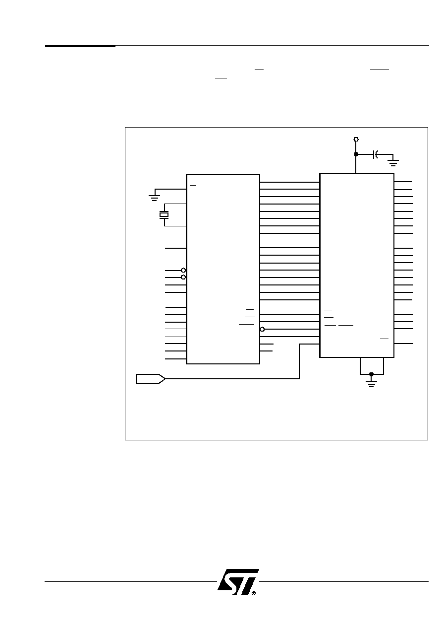
Figure 3A. Connecting a PSD3XX to an 8-Bit Multiplexed-Bus MCU
Your
8-bit
MCU
PSD3XX
PA
PB
PC
AD0 -AD7
A8 -A15
ALE/AS
PSEN
R/ W or WR
RD/E / DS
1
A19 / CSI
RESET
A16-A18
2
Figure 3B. Connecting a PSD3XX to a 16-Bit Multiplexed-Bus MCU
Your
16-bit
MCU
PSD3XX
PA
PB
PC
AD0 -AD7
AD8 -AD15
ALE/AS
BHE/ PSEN
R/ W or WR
RD/E / DS
1
A19 / CSI
RESET
A16-A18
2
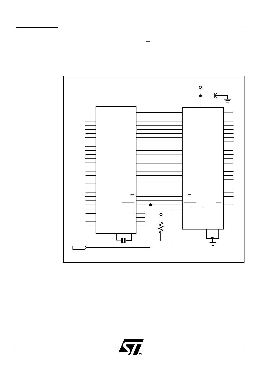
Figure 3C. Connecting a PSD3XX to an 8-Bit Non-Multiplexed-Bus MCU
Your
8-bit
MCU
PSD3XX
PA
PB
PC
D0 -D7
A0-A15
ALE/AS
PSEN
R/ W or WR
RD/E / DS
1
A19 / CSI
RESET
A16-A18
2
Figure 3D. Connecting a PSD3XX to a 16-Bit Non-Multiplexed-Bus MCU
Your
16-bit
MCU
PSD3XX
PA
PB
PC
D0 -D15
A0-A15
ALE/AS
BHE / PSEN
R/ W or WR
RD/E / DS
1
A19 / CSI
RESET
A16-A18
2
D0 -D7
D8-D15
NOTES: 1. DS is a valid input on 3X2/3X3 and devices only.
2. Connect A16-A18 to Port C if your MCU outputs more than 16 bits of address.
8.0
Operating Modes
(MCU
Configurations)
(cont.)

PSD3XX Family
12
Multiplexed Address/Data
Non-Multiplexed Address/Data
8-bit Data Bus
I/O or low-order address
Port A
lines or Low-order multiplexed
D0≠D7 data bus byte
address/data byte
Port B
I/O and/or CS0≠CS7
I/O and/or CS0≠CS7
AD0/A0≠AD7/A7
Low-order multiplexed
address/data byte
Low-order address bus byte
AD8/A8≠AD15/A15
High-order address
High-order address bus byte
bus byte
16-bit Data Bus
I/O or low-order address
Port A
lines or low-order multiplexed
Low-order data bus byte
address/data byte
Port B
I/O and/or CS0≠CS7
High-order data bus byte
AD0/A0≠AD7/A7
Low-order multiplexed
address/data byte
Low-order address bus byte
AD8/A8≠AD15/A15
High-order multiplexed
address/data byte
High-order address bus byte
8.0
Operating
Modes (MCU
Configurations)
(cont.)
Table 3. Bus and Port Configuration Options
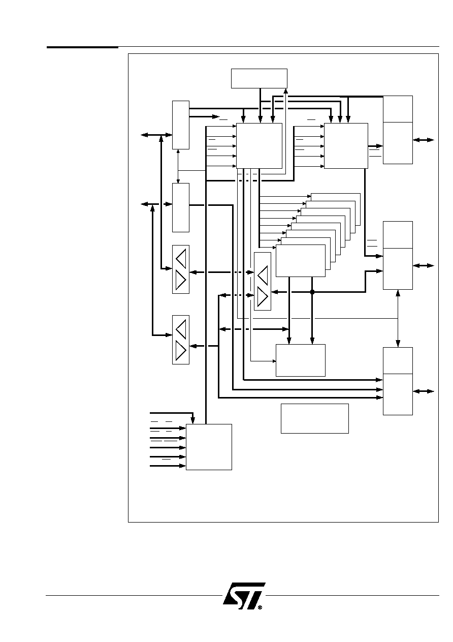
9.0
Programmable
Address
Decoder (PAD)
The PSD3XX contains two programmable arrays, referred to as PAD A and PAD B
(Figure 4). PAD A is used to generate chip select signals derived from the input address to
the internal EPROM blocks, SRAM, I/O ports, and Track Mode signals.
PAD B outputs to Ports B and C for off-chip usage. PAD B can also be used to extend the
decoding to select external devices or as a random logic replacement.
PAD A and PAD B receive the same inputs. The PAD logic is configured by PSDsoft
based on the designer's input. The PAD's non-volatile configuration is stored in a
re-programmable CMOS EPROM. Windowed packages are available for erasure by the
user. See Table 4 for a list of PAD A and PAD B functions.

NOTES: 1. CSI is a power-down signal. When high, the PAD is in stand-by mode and all its outputs
become non-active. See Tables 12 and 13.
2. RESET deselects all PAD output signals. See Tables 10 and 11.
3. A18, A17, and A16 are internally multiplexed with CS10, CS9, and CS8, respectively.
Either A18 or CS10, A17 or CS9, and A16 or CS8 can be routed to the external pins of
Port C. Port C pins can be configured as either input or output, individually.
4. P
0
≠P
3
are not included on 3X1 devices.
5. DS is not available on 3X1 devices.
Figure 4.
PAD Description
ALE or AS
WR or R/W
A19
A18
A17
A16
A15
A14
A13
A12
A11
ES0
ES1
ES2
ES3
ES4
ES5
ES6
ES7
RS0
CSIOPORT
CSADIN
CSADOUT1
CSADOUT2
CS0/PB0
CS1/PB1
CS2/PB2
CS3/PB3
CS4/PB4
CS5/PB5
CS6/PB6
CS7/PB7
CS8/PC0
CS9/PC1
CS10/PC2
RD/E/DS
8 EPROM BLOCK
SELECT LINES
CSI
RESET
SRAM BLOCK SELECT
*
TRACK MODE
CONTROL SIGNALS
P
0
P
1
P
2
P
3
I/O BASE ADDRESS
PAD
B
PAD
A
PSD3XX Family
13
*
SRAM no available on "R" versions

PSD3XX Family
14
Function
PAD A and PAD B Inputs
A19/CSI
When the PSD is configured to use CSI and while CSI is a logic 1, the PAD
deselects all of its outputs and enters a power-down mode (see Tables 12
and 13). When the PSD is configured to use A19, this signal is another
input to the PAD.
A16≠A18
These are general purpose inputs from Port C. See Figure 4, Note 3.
A11≠A15
These are address inputs.
P0≠P3
These are inputs from the page register (not available on 3X1 versions).
RD/E/DS
This is the read pulse or strobe input. (DS not available on 3X1 versions).
WR or R/W
This is the write pulse or R/W select signal.
ALE/AS
This is the ALE or AS input to the chip. Use to demultiplex address
and data.
RESET
This deselects all outputs from the PAD; it can not be used in product
term equations. See Tables 10 and 11.
PAD A Outputs
These are internal chip-selects to the 8 EPROM banks. Each bank can
ES0≠ES7
be located on any boundary that is a function of one product term of the
PAD address inputs.
RS0
This is an internal chip-select to the SRAM. Its base address location is
a function of one term of the PAD address inputs.
This internal chip-select selects the I/O ports. It can be placed on any
CSIOPORT
boundary that is a function of one product term of the PAD inputs. See
Tables 5A and 5B.
This internal chip-select, when Port A is configured as a low-order
address/data bus in the track mode controls the input direction of Port A.
CSADIN is gated externally to the PAD by the internal read signal. When
CSADIN
CSADIN and a read operation are active, data presented on Port A
flows out of AD0/A0≠AD7/A7. This chip-select can be placed on any
boundary that is a function of one product term of the PAD inputs.
See Figure 5B.
This internal chip-select, when Port A is configured as a low-order
address/data bus in track mode, controls the output direction of Port A.
CSADOUT1 is gated externally to the PAD by the ALE signal. When
CSADOUT1
CSADOUT1 and the ALE signal are active, the address presented on
AD0/A0≠AD7/A7 flows out of Port A. This chip-select can be placed on
any boundary that is a function of one product term of the PAD inputs.
See Figure 5B.
This internal chip-select, when Port A is configured as a low-order
address/data bus in the track mode, controls the output direction of Port A.
CSADOUT2 must include the write-cycle control signals as part of its
CSADOUT2
product term. When CSADOUT2 is active, the data presented on
AD0/A0≠AD7/A7 flows out of Port A. This chip-select can be placed on
any boundary that is a function of one product term of the PAD inputs.
See Figure 5B.
PAD B Outputs
CS0≠CS3
These chip-select outputs can be routed through Port B. Each of them is
a function of up to four product terms of the PAD inputs.
CS4≠CS7
These chip-select outputs can be routed through Port B. Each of them is
a function of up to two product terms of the PAD inputs.
CS8≠CS10
These chip-select outputs can be routed through Port C. See Figure 4,
Note 3. Each of them is a function of one product term of the PAD inputs.
Table 4.
PSD3XX
PAD A and
PAD B
Functions
15
PSD3XX Family
10.0
I/O Port
Functions
The PSD3XX has three I/O ports (Ports A, B, and C) that are configurable at the bit level.
This permits great flexibility and a high degree of customization for specific applications.
The next section describes the control registers for the ports. Following that are sections
that describe each port. Figures 5 through 7 show the structure of Ports A through C,
respectively.
Note: any unused input should be connected directly to ground or pulled up to V
CC
(using a 10K
to 100K
resistor).
10.1 CSIOPORT Registers
Control of the ports is primarily handled through the CSIOPORT registers. There are 24
bytes in the address space, starting at the base address labeled CSIOPORT. Since the
PSD3XX uses internal address lines A15-A8 for decoding, the CSIOPORT space will
occupy 2 Kbytes of memory, on a 2 Kbyte boundary. This resolution can be improved to
reduce wasted address space by connecting lower order address lines (A7 and below)
to Port C. Using this method, resolution down to 256 Kbytes may be achieved. The
CSIOPORT space must be defined in your PSDsoft design file. The following tables list
the registers located in the CSIOPORT space.
16-Bit Users Note
When referring to Table 5B, realize that Ports A and B are still accessible on a byte basis.
Note: When accessing Port B on a 16-bit data bus, BHE must be low.
Table 5A. CSIOPORT Registers for 8-Bit Data Busses
NOTE: 1. ZPSD only.
Offset (in hex)
Type of
from CSIOPORT
Access
Register Name
Base Address
Allowed
Port A Pin Register
+2
Read
Port A Direction Register
+4
Read/Write
Port A Data Register
+6
Read/Write
Port B Pin Register
+3
Read
Port B Direction Register
+5
Read/Write
Port B Data Register
+7
Read/Write
Power Management Register (Note 1)
+10
Read/Write
Page Register
+18
Read/Write
Table 5B. CSIOPORT Registers for 16-Bit Data Busses
NOTE: 1. ZPSD only.
Offset (in hex)
Type of
from CSIOPORT
Access
Register Name
Base Address
Allowed
Port A/B Pin Register
+2
Read
Port A/B Direction Register
+4
Read/Write
Port A/B Data Register
+6
Read/Write
Power Management Register (Note 1)
+10
Read/Write
Page Register
+18
Read/Write
PSD3XX Family
16
PSD3XX Family
10.0
I/O Port
Functions
(
cont.)
10.2 Port A (PA0-PA7)
The control registers of Port A are located in CSIOPORT space; see Table 5.
10.2.1 Port A (PA0-PA7) in Multiplexed Address/Data Mode
Each pin of Port A can be individually configured. The following table summarizes what the
control registers (in CSIOPORT space) for Port A do:
NOTE: 1. Default value is the value after reset.
Default
Value
Register Name
0 Value
1 Value
(Note 1)
Port A Pin Register
Sampled logic level
Sampled logic level
X
at pin = `0'
at pin = `1'
Port A Direction Register
Pin is configured
Pin is configured
0
as input
as output
Port A Data Register
Data in DFF = `0'
Data in DFF = `1'
0
MCU I/O Mode
The default configuration of Port A is MCU I/O. In this mode, every pin can be set (at run-
time) as an input or output by writing to the respective pin's direction flip-flop (DIR FF,
Figure 5A). As an output, the pin level can be controlled by writing to the respective pin's
data flip-flop (DFF, Figure 5A). The Pin Register can be read to determine logic level of the
pin. The contents of the Pin Register indicate the true state of the PSD driving the pin
through the DFF or an external source driving the pin. Pins can be configured as CMOS
or open-drain using ST's PSDsoft software. Open-drain pins require external pull-up
resistors.
Latched Address Output Mode
Alternatively, any bit(s) of Port A can be configured to output low-order demultiplexed
address bus bit. The address is provided by the internal PSD address latch, which latches
the address on the trailing edge of ALE/AS. Port A then outputs the desired demultiplexed
address bits. This feature can eliminate the need for an external latch (for example:
74LS373) if you have devices that require low-order latched address bits. Although any pin
of Port A may output an address signal, the pin is position-dependent. In other words, pin
PA0 of Port A may only pass A0, PA1 only A1, and so on.
Track Mode
Track Mode sets the entire port to track the signals on AD0/A0-AD7/A7, depending on
specific address ranges defined by the PAD's CSADIN, CSADOUT1, and CSADOUT2
signals. This feature lets the user interface the microcontroller to shared external resources
without requiring external buffers and decoders. In Track Mode, Port A effectively operates
as a bi-directional buffer, allowing external MCUs or host processors to access the local
data bus. Keep the following information in mind when setting up Track Mode:
t
The direction is controlled by:
∑
ALE/AS
∑
RD/E or RD/E/DS (DS on non-3X1 devices only)
∑
WR or R/W
∑
PAD outputs CSADOUT1, CSADOUT2, and CSADIN defined in PSDsoft design.
t
When CSADOUT1 and ALE/AS are true, the address on AD0/A0-AD7/A7 is output on
Port A. Note: carefully check the generation of CSADOUT1 to ensure that it is stable
during the ALE/AS pulse.
t
When CSADOUT2 is active and a write operation is performed, the data on the
AD0/A0-AD7/A7 input pins flows out through Port A.
t
When CSADIN is active and a read operation is performed, the data on Port A flows
out through the AD0/A0-AD7/A7 pins.
t
Port A is tri-stated when none of the above conditions exist.

NOTE: 1. The expression for CSADOUT2 must include the following write operation cycle signals:
For CRRWR = 0, CSADOUT2 must include WR = 0.
For CRRWR = 1, CSADOUT2 must include E = 1 and R/W = 0.
PSD3XX Family
17
INTERNAL
READ
CSADIN
INTERNAL
ALE
PA0 ≠ PA7
A11≠ A15
A16 ≠ A19
AD8≠ AD15
CSADOUT1
CSADOUT2
(1)
ALE or AS
AD0 ≠AD7
RD / E
WR or R / W
CONTROL
DECODER
LATCH
PAD
I
O
NOTE: 1. CMOS/OD determines whether the output is open drain or CMOS.
READ PIN
PORT A PIN
ENABLE
LATCHED
ADDR OUT
MCU
I/O
OUT
ADn/ Dn
READ DATA
WRITE DATA
ALE
READ DIR
WRITE DIR
RESET
CK
D
R
G
D
R
D
CK
R
CMOS / OD
(1)
I
N
T
E
R
N
A
L
A
D
D
R
/
D
A
T
A
B
U
S
A
D
0
/
A
D
7
DFF
LATCH
DIR
FF
CONTROL
MUX
10.2.2 Port A (PA0-PA7) in Non-Multiplexed Address/Data Mode
In this mode, Port A becomes the low-order data bus byte of the chip. When reading an
internal location, data is presented on Port A pins to the MCU. When writing to an internal
location, data present on Port A pins from the MCU is written to the desired location.
10.0
I/O Port
Functions
(
cont.)
Figure 5A. Port A Pin Structure
Figure 5B. Port A Track Mode

PSD3XX Family
18
PSD3XX Family
10.
I/O Port
Functions
(
cont.)
10.3 Port B (PB0-PB7)
The control registers of Port B are located in CSIOPORT space; see Table 5A and 5B.
10.3.1 Port B (PB0-PB7) in Multiplexed Address/Data Mode
Each pin of Port B can be individually configured. The following table summarizes what the
control registers (in CSIOPORT space) for Port B do:
NOTE: 1. Default value is the value after reset.
Default
Value
Register Name
0 Value
1 Value
(Note 1)
Port B Pin Register
Sampled logic level
Sampled logic level
X
at pin = `0'
at pin = `1'
Port B Direction Register
Pin is configured
Pin is configured
0
as input
as output
Port B Data Register
Data in DFF = `0'
Data in DFF = `1'
0
MCU I/O Mode
The default configuration of Port B is MCU I/O. In this mode, every pin can be set
(at run-time) as an input or output by writing to the respective pin's direction flip-flop (DIR
FF, Figure 6). As an output, the pin level can be controlled by writing to the respective pin's
data flip-flop (DFF, Figure 6). The Pin Register can be read to determine logic level of the
pin. The contents of the Pin Register indicate the true state of the PSD driving the pin
through the DFF or an external source driving the pin. Pins can be configured as CMOS
or open-drain using ST's PSDsoft software. Open-drain pins require external pull-up
resistors.
Chip Select Output
Alternatively, each bit of Port B can be configured to provide a chip-select output signal
from PAD B. PB0-PB7 can provide CS0-CS7, respectively. The functionality of these pins is
not limited to chip selects only; they can be used for generic combinatorial logic as well.
Each of the CS0-CS3 signals is comprised of four product terms, and each of the CS4-CS7
signals is comprised of two product terms.
PSD3XX Family
19
PSD3XX Family
READ PIN
READ DATA
PORT B PIN
CMOS/OD
(1)
MCU
I/O
OUT
WRITE DATA
CK
D
R
DFF
ENABLE
MUX
Dn
CSn
CONTROL
DIR
FF
D
CK
R
WRITE DIR
RESET
READ DIR
I
N
T
E
R
N
A
L
I
N
T
E
R
N
A
L
C
S
O
U
T
D
A
T
A
B
U
S
B
U
S
C
S
0
∑
∑
∑
7
D
8
∑
∑
∑
D
1
5
NOTE: 1. CMOS/OD determines whether the output is open drain or CMOS.
Figure 6. Port B Pin Structure
10.3.2 Port B (PB0-PB7) in 16-bit Multiplexed Address/Data Mode
In this mode, Port B becomes the low-order data bus byte to the MCU chip. When reading
an internal high-order location, data is presented on Port B pins to the MCU. When writing
to an internal high-order location, data present on Port B pins from the MCU is written to the
desired location.
10.
I/O Port
Functions
(
cont.)

PSD3XX Family
20
CS8 / CS9 / C S10
From PAD
To PAD
A16/A17/A18
Latched Address
Input
Q
D
En
Logic Input
D
E
M
U
X
Address In or
Chip Select Out
Input or Output
Set by PSDsoft
2
PSDsoft
2
Port C I/O
1
(PC0 / P C1/ P C2)
ALE
NOTES: 1. Port C pins can be individually configured as inputs or outputs, but not both. Pins can be individually
configured as address or logic and latched or transparent, except for the 3X1 devices, which must be
set to all address or all logic.
2. PSDsoft sets this configuration prior to run-time based on your PSDsoft design file.
Figure 7. Port C (PC0-PC2) Pin Structure
10.4 Port C (PC0-PC2)
Each pin of Port C (Figure 7) can be configured as an input to PAD A and PAD B, or as an
output from PAD B. As inputs, the pins are referenced as A16-A18. Although the pins are
given this reference, they can be used for any address or logic input. [For example, A8-A10
could be connected to those pins to improve the resolution (boundaries) of CS0-CS7 to 256
bytes.] How they are defined in the PSDsoft design file determines:
∑
Whether they are address or logic inputs
∑
Whether the input is transparent or latched by the trailing edge of ALE/AS.
Notes:
1) If the inputs are addresses, they are routed to PAD A and PAD B, and can be used in
any or all PAD equations.
2) A logic input is routed to PAD B and can be used for Boolean equations that are
implemented in any or all of the CS0-CS10 PAD B outputs.
Alternately, PC0-PC2 can become CS8-CS10 outputs, respectively, providing the user with
more external chip-select PAD outputs. Each of the signals (CS8-CS10) is comprised of
one product term.
10.
I/O Port
Functions
(
cont.)
10.5 ALE/AS Input Pin
The ALE/AS pin may be used as a generic logic input signal to the PADs if a
non-multiplexed MCU configuration is chosen in PSDsoft.

PSD3XX Family
21
11.
PSD Memory
The following sections explain the various memory blocks and memory options within the
PSD3XX.
11.1 EPROM
For all of the PSD3XX devices, the EPROM is built using Zero-power technology. This
means that the EPROM powers up only when the address changes. It consumes power for
the necessary time to latch data on its outputs. After this, it powers down and remains in
Standby Mode until the next address change. This happens automatically, and the designer
has to do nothing special.
The EPROM is divided into eight equal-sized banks. Each bank can be placed in any
address location by programming the PAD. Bank0-Bank7 are selected by PAD A outputs
ES0-ES7, respectively. There is one product term for each bank select (ESi).
Refer to Table 1 to see the size of the EPROM for each PSD device.
11.2 SRAM (Optional)
Like the EPROM, the optional SRAM in the PSD3XX devices is built using Zero-power
technology.
All PSD3XX parts which do not have an R suffix contain 2 Kbytes of SRAM (Table 1). The
SRAM is selected by the RS0 output of the PAD. There is one product term dedicated to
RS0.
If your design requires a SRAM larger than 2K x 8, then use one of the RAMless
(R versions) of the 3XX devices with an external SRAM. The external SRAM can be
addressed trhough Port A and all require logic will be taken care of by the PSD3XXR.
11.3 Page Register (Optional)
All PSD3XX parts, except 3X1devices, have a four-bit page register. Thus the effective
address space of your MCU can be enlarged by a factor of 16. Each bit of the Page
Register can be individually read or written. The Page Register is located in CSIOPORT
space (at offset 18h); see Table 5. The Page Register is connected to the lowest nibble of
the data bus (D3-D0). The outputs of the Page Register, P3-P0, are connected to PAD A,
and therefor can be used in any chip select (internal or external) equations. The contents of
the page register are reset to zero at power-up and after any chip-level reset.
11.4 Programming and Erasure
Programming the device can be done using the following methods:
∑ST
's main programmer--PSDpro--which is accessible through a parallel port.
∑
ST's programmer used specifically with the PSD3XX--PEP300.
∑ST
's discontinued programmer--Magic Pro.
∑
A 3rd party programmer, such as Data I/O.
Information for programming the device is available directly from ST. Please contact your
local sales representative. Also, check our web site (www.st.com/psm) for information related
to 3rd party programmers.
Upon delivery from ST or after each erasure (using windowed part), the PSD3XX device
has all bits in PAD and EPROM in the HI state (logic 1). The configuration bits are in the LO
state (logic 0).
To clear all locations of their programmed contents (assuming you have a windowed
version), expose the windowed device to an Ultra-Violet (UV) light source. A dosage of
30 W second/cm
2
is required for PSD3XX devices, and 40 W second/cm
2
for low-voltage
(V suffix) devices. This dosage can be obtained with exposure to a wavelength of 2537 ≈
and intensity of 12000 µW/cm
2
for 40 to 45 minutes for the PSD3XX and 55 to 60 minutes
for the low-voltage (V suffix) devices. The device should be approximately 1 inch (2.54 cm)
from the source, and all filters should be removed from the UV light source prior to erasure.
The PSD3XX devices will erase with light sources having wavelengths shorter than 4000 ≈.
However, the erasure times will be much longer than when using the recommended 2537 ≈
wavelength. Note: exposure to sunlight will eventually erase the device. If used in such an
environment, the package window should be covered with an opaque substance.
PSD3XX Family
22
12.0
Control Signals
Consult your MCU data sheet to determine which control signals your MCU generates, and
how they operate. This section is intended to show which control signals should be
connected to what pins on the PSD3XX. You will then use PSDsoft to configure the
PSD3XX, based on the combination of control signals that your MCU outputs, for example
RD, WR, and PSEN.
The PSD3XX is compatible with the following control signals:
∑
ALE or AS (polarity is programmable)
∑
WR or R/W
∑
RD/E or RD/E/DS (DS for non-3X1 devices only)
∑
BHE or PSEN
∑
A19/CSI
∑
RESET (polarity is programmable except on low voltage versions with the V suffix).
12.1 ALE or AS
Connect the ALE or AS signal from your MCU to this pin where applicable, and program
the polarity using PSDsoft. The trailing edge (when the signal goes inactive) of ALE or AS
latches the address on any pins that have an address input. If you are using a
non-multiplexed-bus MCU that does not output an ALE or AS signal, this pin can be used
for a generic input to the PAD. Note: if your data is multiplexed with address lines other
than A0-A7, connect your address pins to AD0/A0-AD15/A15, and connect your data to
Port A (and Port B where applicable), and connect the ALE/AS signal to this pin.
12.2 WR or R/W
Your MCU should output a stand-alone write signal (WR) or a multiplexed read/write signal
(R/W). In either case, the signal should be connected to this pin.
12.3 RD/E/DS (DS option not available on 3X1 devices)
Your MCU should output any one of RD, E (clock), or DS. In any case, connect the
appropriate signal to this pin.
12.4 BHE or PSEN
t
If your MCU does not output either of these signals, tie this pin to Vcc
(through a series resistor), and skip to the next signal.
t
If you use an 8-bit 8031 compatible MCU that outputs a separate signal when
accessing program space, such as PSEN, connect it to this pin. You would then use
PSDsoft to configure the EPROM in the PSD3XX to respond to PSEN only or PSEN
and RD. If you have an 8031 compatible MCU, refer to the "Program/Data Space and
the 8031" section for further information.
t
If you are using a 16-bit MCU, connect the BHE (or similar signal) output to this pin.
BHE enables accessing of the upper byte of the data bus. See Table 6 for information
on how this signal is used in conjunction with the A0 address line.
BHE
A
0
Operation
0
0
Whole Word
0
1
Upper Byte From/To Odd Address
1
0
Lower Byte From/To Even Address
1
1
None
Table 6. Truth Table for BHE and Address Bit A0 (16-bit MCUs only)
PSD3XX Family
23
12.0
Control Signals
(cont.)
12.5 A19/CSI
This pin is configured using PSDsoft to be either a chip select for the entire PSD device or
an additional PAD input. If your MCU can generate a chip-select signal, and you wish to
save power, use the PSD chip select feature. Otherwise, use this pin as an address or logic
input.
t
When configured as CSI (active-low PSD chip select): a low on this pin keeps the PSD
in normal operation. However, when a high is detected on the pin, the PSD
enters Power-down Mode. See Tables 7A and 7B for information on signal states
during Power-down Mode. See section 16 for details about the reduction of power
consumption.
t
When configured as A19, the pin can be used as an additional input to the PADs.
It can be used for address or logic. It can also be ALE/AS dependent or a transparent
input, which is determined by your PSDsoft design file. In A19 mode, the PSD is always
enabled.
Port
Configuration Mode(s)
State
AD0≠A0/AD15/A15
All
Input (Hi-Z)
MCU I/O
Unchanged
Port Pins PA0≠PA7
Tracking AD0/A0-AD7/A7
Input (Hi-Z)
Latched Address Out
Logic 1
MCU I/O
Unchanged
Port Pins PB0≠PB7
Chip Select Outputs, CS0≠CS7, CMOS
Logic 1
Chip Select Outputs, CS0≠CS7, Open Drain
Hi-Z
Port Pins PC0≠PC2
Address or Logic Inputs, A16-A18
Input (Hi-Z)
Chip Select Outputs, CS8≠CS10, CMOS only
Logic 1
Table 7A. Signal States During Power-Down Mode
Internal Signal State
Component
Internal Signal
During Power-Down
PAD A and PAD B
CS0≠CS10
Logic 1 (inactive)
CSADIN, CSADOUT1,
CSADOUT2, CSIOPORT,
Logic 0 (inactive)
ES0-ES7, RS0
All registers in CSIOPORT
N/A
address space, including:
Direction
Data
All unchanged
Page
PMR (turbo bit, ZPSD only)
Table 7B. Internal States During Power-down
NOTE: N/A = Not Applicable

PSD3XX Family
24
12.0
Control Signals
(cont.)
12.6 Reset Input
This is an asynchronous input to initialize the PSD device.
Refer to tables 8A and 8B for information on device status during and after reset.
The standard-voltage PSD3XX and ZPSD3XX (non-V) devices require a reset input that
is asserted for at least 100 nsec. The PSD will be functional immediately after reset is
de-asserted. For these standard-voltage devices, the polarity of the reset input signal is
programmable using PSDsoft (active-high or active-low), to match the functionality of your
MCU reset.
Note: It is not recommended to drive the reset input of the MCU and the reset input of the
PSD with a simple RC circuit between power on ground. The input threshold of the MCU
and the PSD devices may differ, causing the devices to enter and exit reset at different
times because of slow ramping of the signal. This may result in the PSD not being
operational when accessed by the MCU. It is recommended to drive both devices actively.
A supervisory device or a gate with hysteresis is recommended.
For low-voltage ZPSD3XXV devices only, the reset input must be asserted for at least
500 nsec. The ZPSD3XXV will not be functional for an additional 500 nsec after reset is
de-asserted (see Figure 8). These low voltage ZPSD3XXV devices must use an active-low
polarity signal for reset. Unlike the standard PSDs, the reset polarity for the ZPSD3XXV is
not programmable. If your MCU operates with an active high reset, you must invert this
signal before driving the ZPSD3XXV reset input.
You must design your system to ensure that the PSD comes out of reset and the PSD is
active before the MCU makes its first access to PSD memory. Depending on the
characteristics and speed of your MCU, a delay between the PSD reset and the MCU reset
may be needed.
Signal State Just
Signal State
After Reset
Port
Configured Mode of Operation
During Reset
(Note 1)
AD0/A0-
All
Input (Hi-Z)
MCU address
AD15/A15
and/or data
MCU I/O
Input (Hi-Z)
Input (Hi-Z)
Tracking
Input (Hi-Z)
Active Track
Port Pins
AD0/A0-AD7/A7
Mode
PA0-PA7
PSD3XX,
Logic 0
MCU address
Latched Address Out
ZPSD3XX
ZPSD3XXV
Hi-Z
MCU address
MCU I/O
Input (Hi-Z
Input (Hi-Z)
Chip Select Outputs,
PSD3XX,
Logic 1
Per CS equations
Port Pins
CS0-CS7, CMOS
ZPSD3XX
PB0-PB7
ZPSD3XXV
Hi-Z
Per CS equations
Chip Select Outputs,
PSD3XX,
Hi-Z
Per CS equations
CS0-CS7, Open Drain
ZPSD3XX
ZPSD3XXV
Hi-Z
Per CS equations
Address or Logic Inputs, A16-A18
Input (Hi-Z)
Input (Hi-Z)
Port Pins
Chip Select Outputs,
PSD3XX,
Logic 1
Per CS equations
PC0-PC2
CS8-CS10, CMOS
ZPSD3XX
ZPSD3XXV
Hi-Z
Per CS equations
Table 8A. External PSD Signal States During and Just After Reset
NOTE: 1. Signal is valid immediately after reset for PSD3XX and ZPSD3XX devices. ZPSD3XXV devices need an
additional 500 nsec after reset before signal is valid.
PSD3XX Family
25
12.0
Control Signals
(cont.)
Internal
Internal Signal
Signal State
State During
During
Component
Internal Signal
Reset
Power-Down
CS0-CS10
Logic 1 (inactive)
Per CS Equations
CSADIN,
CSADOUT1,
Per equations
PAD A and PAD B
CSADOUT2,
Logic 0 (inactive)
for each
CSIOPORT,
internal signal
ES0-ES7, RS0
All registers in CSIOPORT
address space, including:
Direction
Logic 0 in all bit of
Logic 0 until
Data
N/A
all registers
changed by MCU
Page
PMR (turbo bit,
ZPSD3XX only)
Table 8B. Internal PSD Signal States During and Just After Reset
NOTE: N/A = Not Applicable
RESET LOW
V
IH
RESET HIGH
ZPSD3XXV
IS OPERATIONAL
500 ns
500 ns
V
IL
Figure 8. The Reset Cycle (RESET) (ZPSD3XXV Versions)
PSD3XX Family
26
13.0
Program/Data
Space and the
8031
This section only applies to users who have an 8031 or compatible MCU that outputs a
signal such as PSEN when accessing program space. If this applies to you, be aware of the
following:
t
The PSD3XX can be configured using PSDsoft such that the EPROM is either
1) accessed by PSEN only (Figure 10); or 2) accessed by PSEN or RD (Figure 9).
The default is PSEN only unless changed in PSDsoft.
t
The SRAM and I/O Ports (including CSIOPORT) can not be placed in program space
only. By default, they are in data space only (Figure 10). However, the SRAM may
be placed in Program and Data Space, as shown in Figure 9.
Figure 9. Combined Address Space
INTERNAL
OE
OE
OE
CS
CS
CS
RD
ADDRESS
PSEN
I/O PORTS
PAD
SRAM
*
EPROM
INTERNAL
OE
OE
OE
CS
CS
CS
RD
ADDRESS
PSEN
I/O PORTS
PAD
SRAM
*
EPROM
Figure 10. 8031-Compatible Separate Code and Data Address Spaces
*
Not available on "R" versions.
*
Not available on "R" versions.
PSD3XX Family
27
14.0
System
Applications
In Figure 11, the PSD3XX is configured to interface with Intel's 80C31, which is a 16-bit
address/8-bit data bus microcontroller. Its data bus is multiplexed with the low-order
address byte. The 80C31 uses signals RD to read from data memory and PSEN to read
from code memory. It uses WR to write into the data memory. It also uses active high reset
and ALE signals. The rest of the configuration bits, as well as the unconnected signals,
are application specific, and thus, user dependent.
MICROCONTROLLER
31
19
18
9
12
13
14
15
1
2
3
4
5
6
7
8
23
24
25
26
27
28
29
30
31
32
33
35
36
37
38
39
22
2
1
13
3
P0.0
P0.1
P0.2
P0.3
P0.4
P0.5
P0.6
P0.7
P2.0
P2.1
P2.2
P2.3
P2.4
P2.5
P2.6
P2.7
RD
WR
PSEN
ALE
TXD
RXD
PA0
PA1
PA2
PA3
PA4
PA5
PA6
PA7
PB0
PB1
PB2
PB3
PB4
PB5
PB6
PB7
PC0
PC1
PC2
A19/CSI
39
38
37
36
35
34
33
32
21
22
23
24
25
26
27
28
17
16
29
30
11
10
21
20
19
18
17
16
15
14
11
10
9
8
7
6
5
4
40
41
42
43
EA/VP
X1
X2
RESET
INT0
INT1
T0
T1
P1.0
P1.1
P1.2
P1.3
P1.4
P1.5
P1.6
P1.7
AD0/A0
AD1/A1
AD2/A2
AD3/A3
AD4/A4
AD5/A5
AD6/A6
AD7/A7
AD8/A8
AD9/A9
AD10/A10
AD11/A11
AD12/A12
AD13/A13
AD14/A14
AD15/A15
RD
WR/V
PP
BHE/PSEN
ALE
RESET
GND
PSD3XX
80C31
34
12
VCC
44
0.1µF
Reset
NOTE: RESET to the PSD3XX must be the output of a RESET chip or buffer.
If RESET to the 80C31 is the output of an RC circuit, a separate buffered RC RESET to the
PSD3XX (shorter than the 80C31 RC RESET) must be provided to avoid a race condition.
Figure 11. PSD3XX Interface With Intel's 80C31
PSD3XX Family
28
14.0
System
Applications
(cont.)
In Figure 12, the PSD3XX is configured to interface with Motorola's 68HC11, which is a
16-bit address/8-bit data bus microcontroller. Its data bus is multiplexed with the low-order
address byte. The 68HC11 uses E and R/W signals to derive the read and write strobes.
It uses the Address Strobe (AS) for the address latch pulse. RESET is an active-low signal.
The rest of the configuration bits, as well as the unconnected signals, are specific, and thus,
user dependent.
MICROCONTROLLER
20
21
22
23
24
25
43
45
47
49
44
46
48
50
34
33
32
31
30
29
28
27
52
51
23
24
25
26
27
28
29
30
31
32
33
35
36
37
38
39
22
2
13
3
1
PC0
PC1
PC2
PC3
PC4
PC5
PC6
PC7
PB0
PB1
PB2
PB3
PB4
PB5
PB6
PB7
E
R/W
AS
RESET
XIRQ
IRQ
MODB
MODA
PA0
PA1
PA2
PA3
PA4
PA5
PA6
PA7
PB0
PB1
PB2
PB3
PB4
PB5
PB6
PB7
PC0
PC1
PC2
A19/CSI
9
10
11
12
13
14
15
16
42
41
40
39
38
37
36
35
5
6
4
17
18
19
2
3
21
20
19
18
17
16
15
14
11
10
9
8
7
6
5
4
40
41
42
43
PD0
PD1
PD2
PD3
PD4
PD5
PE0
PE1
PE2
PE3
PD4
PE5
PE6
PE7
PA0
PA1
PA2
PA3
PA4
PA5
PA6
PA7
VRH
VRL
AD0/A0
AD1/A1
AD2/A2
AD3/A3
AD4/A4
AD5/A5
AD6/A6
AD7/A7
AD8/A8
AD9/A9
AD10/A10
AD11/A11
AD12/A12
AD13/A13
AD14/A14
AD15/A15
E
R/W/V
PP
AS
RESET
BHE/PSEN
GND
RESET
PSD3XX
34
12
V
CC
V
CC
68HC11
XTAL EXTAL
44
0.1µF
Figure 12. PSD3XX Interface With Motorola's 68HC11
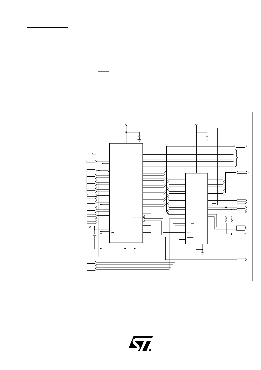
PSD3XX Family
29
14.0
System
Applications
(cont.)
In Figure 13, the PSD3XX is configured to work directly with Intel's 80C196KB
microcontroller, which is a 16-bit address/16-bit data bus processor. The Address and data
lines multiplexed. The PSD3XX is configured to use PC0, PC1, PC2, and A19/CSI as logic
inputs. These signals are independent of the ALE pulse (latch-transparent). They are used
as four general-purpose inputs that take part in the PAD equations.
Port A is configured to work in Track Mode, in which (for certain conditions) PA0≠PA7 tracks
lines AD0/A0≠AD7/A7. Port B is configured to generate CS0≠CS7. In this example, PB2
serves as a WAIT signal that slows down the 80C196KB during the access of external
peripherals. These 8-bit wide peripherals are connected to the shared bus of Port A. The
WAIT signal also drives the buswidth input of the microcontroller, so that every external
peripheral cycle becomes an 8-bit data bus cycle. PB3 and PB4 are open-drain output
signals; thus, they are pulled up externally.
67
68
36
NMI
RxD
TxD
+5V
RST
66
XTAL1
AD[0 ..15]
AD[0 ..15]
XTAL2
3
43
64
14
16
NMI
READY
BUSWIDTH
CDE
RESET
6
5
7
4
11
10
8
9
P0.0
P0.1
P0.2
P0.3
P0.4
P0.5
P0.6
P0.7
18
17
15
44
42
39
33
38
P2.0/TXD
P2.1/RXD
P2.2/EXINT
P2.3/T2CLK
P2.4/T2RST
P2.5/PWM
P2.6/ T2 UP/DN
P2.7/ T2 CAPTR
AD0/A0
AD1/A1
AD2/A2
AD3/A3
AD4/A4
AD5/A5
AD6/A6
AD7/A7
AD8/A8
AD9/A9
AD10/A10
AD11/A11
AD12/A12
AD13/A13
AD14/A14
AD15/A15
21
20
19
18
17
16
15
14
11
10
9
8
7
6
5
4
PA0
PA1
PA2
PA3
PA4
PA5
PA6
PA7
PB0
PB1
PB2
PB3
PB4
PB5
PB6
PB7
AD0/A0
AD1/A1
AD2/A2
AD3/A3
AD4/A4
AD5/A5
AD6/A6
AD7/A7
AD8/A8
AD9/A9
AD10/A10
AD11/A11
AD12/A12
AD13/A13
AD14/A14
AD15/A15
AD0/A0
AD1/A1
AD2/A2
AD3/A3
AD4/A4
AD5/A5
AD6/A6
AD7/A7
AD8/A8
AD9/A9
AD10/A10
AD11/A11
AD12/A12
AD13/A13
AD14/A14
AD15/A15
23
24
25
26
27
28
29
30
31
32
33
35
36
37
38
39
40
41
42
43
1
2
22
13
3
PC0
PC1
PC2
A19/CSI
BHE /PSEN
WR / VPP
RD
ALE
RESET
24
25
26
27
HSI.0
HSI.1
HSI.2/HSO.4
HSI.3/HSO.5
13
37
12
2
VREF
VPP
ANGND
EA
19
20
21
22
23
30
31
32
60
59
58
57
56
55
54
53
52
51
50
49
48
47
46
45
65
41
40
61
62
63
28
29
34
35
P1.0
P1.1
P1.2
P1.3
P1.4
P1.5
P1.6
P1.7
P3.0/AD0
P3.1/AD1
P3.2/AD2
P3.3/AD3
P3.4/AD4
P3.5/AD5
P3.6/AD6
P3.7/AD7
P4.0/AD8
P4.1/AD9
P4.2/AD10
P4.3/AD11
P4.4/AD12
P4.5/AD13
P4.6/AD14
P4.7/AD15
CLKOUT
BHE / WRH
WR / WRL
RD
ALE /ADV
INST
HSO.0
HSO.1
HSO.2
HSO.3
0.1µF
0.1µF
FOUR
GENERAL
PURPOSE
INPUTS
GND GND
12
34
+5V
+5V
+5V
4.7K
4.7K
0.1µF
ALE
WAIT
SHARED
BUS
PORT 1
I/O PINS
44
VCC
VCC
VSS
VSS
ADDRESS/DATA
MULTIPLEXED BUS
80C196KB
PSD3XX
Figure 13. PSD3XX Interface With Intel's 80C196KB

PSD3XX Family
30
15.0
Security Mode
Security Mode in the PSD3XX locks the contents of PAD A, PAD B, and all the configuration
bits. The EPROM, optional SRAM, and I/O contents can be accessed only through the
PAD. The Security Mode must be set by PSDsoft prior to run-time. The Security Bit can only
be erased on the UV parts using a full-chip erase. If Security Mode is enabled, the contents
of the PSD3XX can not be uploaded (copied) on a device programmer.
16.0
Power
Management
PSDs from all PSD3XX families use Zero-power memory techniques that place memory
into Standby Mode between MCU accesses. The memory becomes active briefly after an
address transition, then delivers new data to the outputs, latches the outputs, and returns to
Standby. This is done automatically and the designer has to do nothing special to benefit
from this feature.
In addition to the benefits of Zero-power memory technology, there are ways to gain addi-
tional savings. The following factors determine how much current the entire PSD device
uses:
∑
Use of CSI (Chip Select Input)
∑
Setting of the CMiser bit
∑
Setting of the Turbo Bit (ZPSD only)
∑
The number of product terms used in the PAD
∑
The composite frequency of the input signals to the PAD
∑
The loading on I/O pins.
The total current consumption for the PSD is calculated by summing the currents from
memory, PAD logic, and I/O pins, based on your design parameters and the power
management options used.
16.1 CSI Input
Driving the CSI pin inactive (logic 1) disables the inputs of the PSD and forces the entire
PSD to enter Power-down Mode, independent of any transition on the MCU bus (address
and control) or other PSD inputs. During this time, the PSD device draws only standby
current (micro-amps). Alternately, driving a logic 0 on the CSI pin returns the PSD to normal
operation. See Tables 7A and 7B for information on signal states during Power-down Mode.
The CSI pin feature is available only if enabled in the PSDsoft Configuration utility.
16.2 CMiser bit
In addition to power savings resulting from the Zero-power technology used in the memory,
the CMiser feature saves even more power under certain conditions. Savings are significant
when the PSD is configured for an 8-bit data path because the CMiser feature turns off half
of the array when memory is being accessed (the memory is divided internally into odd and
even arrays). See the DC characteristics table for current usage related to the CMiser bit.
You should keep the following in mind when using this bit:
∑
Setting of this bit is accomplished with PSDsoft at the design stage, prior to run-time.
∑
Memory access times are extended by 10 nsec for standard voltage (non-V) devices,
and 20 nsec for low voltage (V) devices.
∑
EPROM access: although CMiser offers significant power savings in 8-bit mode
(~50%), CMiser contributes no additional power savings when the PSD is configured
for 16-bits.
∑
SRAM access: CMiser reduces power consumption of PSDs configured for either 8-bit
or 16-bit operation.
PSD3XX Family
31
16.
Power
Management
(cont.)
16.3 Turbo Bit (ZPSD only)
The turbo bit is controlled by the MCU at run-time and is accessed through bit zero of the
Power Management Register (PMR). The PMR is located in CSIOPORT space at offset 10h.
Bit 7
Bit 6
Bit 5
Bit 4
Bit 3
Bit 2
Bit 1
Bit 0
*
*
*
*
*
*
*
Turbo bit
1= OFF
1= OFF
1= OFF
1= OFF
1= OFF
1= OFF
1= OFF
1= OFF
Power Management Register (PMR)
*
Future Configuration bits are reserved and should be set to one when writing to this register.
The default value at reset of all bits in the PMR is logic 0, which means the Turbo feature is
enabled. The PAD logic (PAD A and PAD B) of the PSD will operate at full speed and full
power. When the Turbo Bit is set to logic 1, the Turbo feature is disabled. When disabled,
the PAD logic will draw only standby current (micro-amps) while no PAD inputs change.
Whenever there is a transition on any PAD input (including MCU address and control
signals), the PAD logic will power up and will generate new outputs, latch those outputs,
then go back to Standby Mode. Keep in mind that the signal propagation delay through the
PAD logic increases by 10 nsec for non-V devices, and 20 nsec for V devices while in
non-turbo mode. Use of the Turbo Bit does not affect the operation or power consumption
of memory.
Tremendous power savings are possible by setting the Turbo Bit and going into non-turbo
mode. This essentially reduces the DC power consumption of the PAD logic to zero. It also
reduces the AC power consumption of PAD logic when the composite frequency of all PAD
inputs change at a rate less than 40 MHz for non-V devices, and less than 20 MHz for V
devices. Use Figures 14 and 15 to calculate AC and DC current usage in the PAD with the
Turbo Bit on and off. You will need to know the number of product terms that are used in
your design and you will have to calculate the composite frequency of all signals entering
the PAD logic.
16.4 Number of Product Terms in the PAD Logic
The number of product terms used in your design relates directly to how much current the
PADs will draw. Therefore, minimizing this number will be in your best interest if power is a
concern for you. Basically, the amount of product terms your design will use is based on the
following (see Figure 4):
∑
Each of the EPROM block selects, ES0-ES7 uses one product term (for a total of 8).
∑
The CSIOPORT select uses one product term.
∑
If your part has SRAM (non-R versions), the SRAM select RS0 uses one product term.
∑
The Track Mode control signals (CSADIN, CSADOUT1, and CSADOUT2) each use
one product term if you use these signals.
∑
Port B, pins PB0-PB3 are allocated four product terms each if used as outputs.
∑
Port B, pins PB4-PB7 are allocated two product terms each if used as outputs.
∑
Port C, pins PC0-PC2 are allocated one product term each if used as outputs.
Given the above product term allocation, keep the following points in mind when calculating
the total number of product terms your design will require:
1) The EPROM block selects, CSIOPORT select, and SRAM select will use a product term
whether you use these blocks or not. This means you start out with 10 product terms,
and go up from there.
2) For Port B, if you use a pin as an output and your logic equation requires only one
product term, you still have to include all the available product terms for that pin for
power consumption, even though only one product term is specified. For example, if the
output equation for pin PB0 uses just one product term, you will have to count PB0 as
contributing four product terms to the overall count. With this in mind, you should use
Port C for the outputs that only require one product term and PB4-7 for outputs that
require two product terms. Use pins PB0-3 if you need outputs requiring more than two
product terms or you have run out of outputs.
3) The following PSD functions do not consume product terms: MCU I/O mode, Latched
Address Output, and PAD inputs (logic or address).

PSD3XX Family
32
16.0
Power
Management
(cont.)
16.5 Composite Frequency of the Input Signals to the PAD Logic
The composite frequency of the input signals to the PADs is calculated by considering all
transitions on any PAD input signal (including the MCU address and control inputs). Once
you have calculated the composite frequency and know the number of product terms used,
you can determine the total AC current consumption of the PAD by using Figure 14 or
Figure 15. From the figures, notice that the DC component (f = 0 MHz) of PAD current is
essentially zero when the turbo feature is disabled, and that the AC component increases
as frequency increases.
When the turbo feature is disabled, the PAD logic can achieve low power consumption by
becoming active briefly, only when inputs change. For standard voltage (non-V) devices,
the PAD logic will stay active for 25 nsec after it detects a transition on any input. If there
are more transitions on any PAD input within the 25 nsec period, these transitions will not
add to power consumption because the PAD logic is already active. This effect helps
reduce the overall composite frequency value. In other words, narrowly spaced groups of
transitions on input signals may count as just one transition when estimating the composite
frequency.
Note that the "knee" frequency in Figure 14 is 40 MHz, which means that the PAD will
consume less power only if the composite frequency of all PAD inputs is less than 40 MHz.
When the composite frequency is above 40 MHz, the PAD logic never gets a chance to shut
down (inputs are spaced less than 25 nsec) and no power savings can be achieved. Figure
15 is for low-voltage devices in which the "knee" frequency is 20 MHz.
Take the following steps to calculate the composite frequency:
1) Determine your highest frequency input for either PAD A or PAD B.
2) Calculate the period of this input and use this period as a basis for determining the
composite frequency.
3) Examine the remaining PAD input signals within this base period to determine the
number of distinct transitions.
4) Signal transitions that are spaced further than 25 nsec apart count as a distinct transition
(50 nsec for low-voltage V devices). Signal transitions spaced closer than 25 nsec count
as the same transition.
5) Count up the number of distinct transitions and divide that into the value of the base
period.
6) The result is the period of the composite frequency. Divide into one to get the composite
frequency value.
Unfortunately, this procedure is complicated and usually not deterministic since different
inputs may be changing in various cycles. Therefore, we recommend you think of the
situation that has the most activity on the inputs to the PLD and use this to calculate the
composite frequency. Then you will have a number that represents your best estimate at
the worst case scenario.
Since this is a complicated process, the following example should help.
Example Composite Frequency Calculation
Suppose you had the following circuit:
80C31
(12 MHz
Crystal)
PSD3XX
PA
PB
PC
AD0-AD7
Latched Address
Output (LA0 - LA7)
A8-A15
ALE
RD
WR
PSEN
CSI
3 Inputs: Int, Sel, Rdy
5 MCU I/O Outputs
3 Chip-Select Outputs
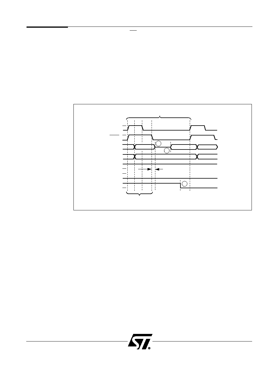
PSD3XX Family
33
All the inputs shown, except CSI, go to the PAD logic. These signals must be taken into
consideration when calculating the composite frequency. Before we make the calculation,
let's establish the following conditions:
∑
The input with the highest frequency is ALE, which is 2 MHz. So our base period is
500 nsec for this example.
∑
Only the address information from the multiplexed signals AD0-AD7 reach the PAD
logic because of the internal address latch. Signal transitions from data on AD0-AD7
do not reach the PADs.
∑
The three inputs (Int, Sel, or Rdy) change state very infrequently relative to the 80C31
bus signals.
Now, lets assume the following is a snapshot in time of all the input signals during a typical
80C31 bus cycle. We'll use a code fetch as an example since that happens most often.
16.0
Power
Management
(cont.)
ONE TYPICAL 80C31 BUS CYCLE (2 MHz, 500 nsec)
ALE
PSEN
AD0-AD7
A8-A15
INT
SEL
RDY
FOUR DISTINCT
TRANSITIONS
< 25 nsec
ADDR
DATA
1
2
3
The calculation of the composite frequency is as follows:
∑
There are four distinct transitions (first four dotted lines) within the base period of
500 nsec. These first four transitions all count toward the final composite frequency.
∑
The transition at (1) in the diagram does not count as a distinct transition because it is
within 25 nsec of a neighboring transition (use 50 nsec for a ZPSD3XXV device).
∑
Transition (2) above does not add to the composite frequency because only the
internally latched address signals reach the PADs, the data signal transitions do not.
∑
The transition at (3) just happens to appear in this snapshot, but its frequency is so
low that it is not a significant contributor to the overall composite frequency, and will
not be used.
∑
Divide the 500 nsec base period by the four (distinct transitions), yielding 125 nsec.
1/125 nsec = 8 MHz.
∑
Use 8 MHz as the composite frequency of PAD inputs when calculating current
consumption. (See the next section for a sample current calculation.)
16.6 Loading on I/O pins
A final consideration when calculating the current usage for the entire PSD device is the
loading on I/O pins. All specifications for PSD current consumption in this document
assume zero current flowing through PSD I/O pins (including ADIO). I/O current is dictated
by the individual design implementation, and must be calculated by the designer. Be aware
that I/O current is a function of loading on the pins and the frequency at which the signals
toggle.

PSD3XX Family
34
Conditions
Part Used
= ZPSD3XX (V
CC
= 5.0 V)
MCU ALE Clock Frequency
= 2.0 MHz
Composite ZPLD Input Frequency
= 8.0 MHz (see example in above section)
% EPROM Access
= 80%
% SRAM Access
= 15%
% I/O access
= 5%
%Time CSI is high (standby mode)
= 90%
%Time CSI is low (normal operation mode)
= 10%
# Product terms used (see previous section) = 13 (13/40 = 33%)
Turbo bit
= OFF (Turbo Mode disabled)
CMiser bit
= ON
MCU Bus Configuration
= 8-bit multiplexed bus mode
Calculation (Based on Typical AC and DC Currents)
I
CC
total = Istandby x % time CSI is high +
[
I
CC
(AC) + I
CC
(DC)
]
x % time CSI is low.
= Istandby x % time CSI is high +
[% EPROM Access x 0.8 mA/MHz x Freq. of ALE
+ % SRAM x 1.4 mA/MHz x Freq of ALE
+ ZPLD AC current (Figure 14: 13 PTs, 8 MHz, Non-Turbo)
]
x % time CSI is low
= 10 µA x 0.9 + (0.8 x 0.8 mA/MHz x 2 MHz + 0.15 x 1.4 mA/MHz x 2 MHz
+ 5.0 mA) x 0.1
= 9.0 µA + (1.28 mA + 0.42 mA + 5.0 mA) x 0.1
= 679 µA, based on the system operating in standby 90% of the time
Once you have read the "Power Management" section, you should be able to calculate
power. The following is a sample power calculation:
17.
Calculating
Power
NOTES: 1. Calculation is based on the assumption that I
OUT
= 0 mA (no I/O pin loading)
2. I
CC
(DC) is zero for all ZPSD devices operating in non-turbo mode.
3. 13 product terms: 8 for EPROM, 3 for Chip Selects, 1 for SRAM, 1 for CSIOPORT.
4. The 5% I/O access in the conditions section is when the MCU accesses CSIOPORT space.
5. Standby Mode can also be achieved without using the CSI pin. The ZPSD device will automatically
go into Standby while no inputs are changing on any pin, and Turbo Mode is disabled.

PSD3XX Family
35
17.0
Calculating
Power
(cont.)
0
0
5
10
15
20
25
30
35
40
45
50
5
10
15
20
25
30
35
40
45
I
CC
(mA
Composite Frequency at PAD Inputs (MHz)
40 PT Turbo
40 PT Non -Turbo
10 PT Turbo
10 PT Non -Turbo
Figure 14. Typical I
CC
vs. Frequency for the PAD (V
CC
= 5 V)
0
0
5
10
15
20
25
2
4
6
8
10
12
14
I
CC
(mA
Composite Frequency at PAD Inputs (MHz)
40 PT Turbo
40 PT Non -Turbo
10 PT Turbo
10 PT Non -Turbo
Figure 15. Typical I
CC
vs. Frequency (V
CC
= 3 V)
PSD3XX Family
36
Figure 18. Normalized I
CC
(AC)
(V
CC
= 3.0 V)
Figure 19. Normalized Access Time (T6)
(V
CC
= 3.0 V)
Figure 16. I
OL
vs. V
OL
(5 V ± 10%)
Figure 17. Normalized I
CC
(DC vs. V
CC
)
(V
CC
= 3.0 V)
40
35
30
25
20
15
10
5
0
0.00
0.10
0.20
0.30
0.40
0.50
0.60
0.70
0.80
VOL (V)
I OL
(mA)
Temp. = 125∞C
Temp. = 25∞C
3.5
3.0
2.5
2.0
1.5
1.0
0.5
I
CC
2.5
3.0
3.5
4.0
4.5
5.0
5.5
6.0
V
CC
(V)
2.7
2.7
2.2
2.0
1.8
1.6
1.4
1.2
1.0
0.8
I
CC
(AC)
2.5
3.0
3.5
4.0
4.5
5.0
5.5
6.0
V
CC
(V)
2.7
1.1
1.05
1.0
0.95
0.9
0.85
0.8
0.75
0.7
0.65
2.5
3.0
3.5
4.0
4.5
5.0
5.5
6.0
ACCESS TIME
V
CC
(V)
ZPSD3XXV
ZPSD3XXV
ZPSD3XXV
ZPSD3XXV
PSD3XX Family
37
Symbol
Parameter
Condition
Min
Max
Unit
T
STG
Storage Temperature
CERDIP
≠ 65
+ 150
∞C
PLASTIC
≠ 65
+ 125
∞C
Voltage on any Pin
With Respect to GND
≠ 0.6
+ 7
V
V
PP
Programming
Supply Voltage
With Respect to GND
≠ 0.6
+ 14
V
V
CC
Supply Voltage
With Respect to GND
≠ 0.6
+ 7
V
ESD Protection
>
2000
V
18.1 Absolute Maximum Ratings
1
NOTE: 1. Stresses above those listed under Absolute Maximum Ratings may cause permanent damage to the
device. This is a stress rating only and functional operation of the device at these or any other
conditions above those indicated in the operational sections of this specification is not implied.
Exposure to Absolute Maximum Rating conditions for extended periods of time may affect device
reliability.
Range
Temperature
V
CC
V
C C
Tolerance
Commercial
0∞ C to +70∞C
+ 3 V
1
, + 5 V
± 10%
Industrial
≠40∞ C to +85∞C
+ 3 V
1
, + 5 V
± 10%
Symbol
Parameter
Conditions
Min
Typ
Max Unit
V
CC
Supply Voltage
ZPSD Versions, All Speeds
4.5
5
5.5
V
V
CC
Supply Voltage
ZPSD V Versions Only,
2.7
3.0
5.5
V
All Speeds
18.2 Operating Range
18.3 Recommended Operating Conditions
NOTES: 1. 3 V version available for ZPSD3XXV devices only.
Symbol
Parameter
Conditions
Typical
2
Max
Unit
C
IN
Capacitance (for input pins only)
V
IN
= 0 V
4
6
pF
C
OUT
Capacitance (for input/output pins)
V
OUT
= 0 V
8
12
pF
C
VPP
Capacitance (for WR/V
PP
or R/W/V
PP
)
V
PP
= 0 V
18
25
pF
NOTES: 1. This parameter is only sampled and is not 100% tested.
2. Typical values are for T
A
= 25∞C and nominal supply voltages.
18.4 Pin Capacitance
1
18.0
Specifications
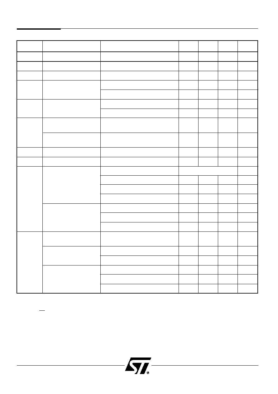
PSD3XX Family
38
NOTES: 1. CMOS inputs: GND ± 0.3 V or V
CC
± 0.3V.
2. TTL inputs: V
IL
0.8 V, V
IH
2.0 V.
3. I
OUT
= 0 mA.
4. CSI/A19 is high and the part is in a power-down configuration mode.
5. All other cases include CMiser = On and 16-bit bus mode and CMiser = Off and 8- or 16-bit bus mode.
Symbol
Parameter
Conditions
Min
Typ
Max
Unit
V
CC
Supply Voltage
All Speeds
4.5
5
5.5
V
V
IH
High-Level Input Voltage
4.5 V < V
CC
> 5.5 V
2
V
CC
+ .1
V
V
IL
Low-Level Input Voltage
4.5 V < V
CC
> 5.5 V
≠ 0.5
0.8
V
I
OH
= ≠ 20 µA, V
CC
= 4.5 V
4.4
4.49
V
V
OH
Output High Voltage
I
OH
= ≠ 2 mA, V
CC
= 4.5 V
2.4
3.9
V
Output Low Voltage
I
OL
= 20 µA, V
CC
= 4.5 V
0.01
0.1
V
V
OL
(See Figure 16)
I
OL
= 8 mA, V
CC
= 4.5 V
0.15
0.45
V
ZPSD3XX
10
20
µA
I
SB
Standby Supply Current
(Notes 1,4)
PSD3XX
Standby Supply Current
50
100
µA
I
LI
Input Leakage Current
V
SS
< V
IN
> V
CC
≠1
±.1
1
µA
I
LO
Output Leakage Current
.45 < V
IN
> V
CC
≠10
± 5
10
µA
ZPLD Turbo Mode = Off, f = 0 MHz
See I
SB
µA
ZPSD3XX
ZPLD Turbo Mode = On, f = 0 MHz
0.5
1
mA/PT
Operating Suppy Current
EPROM, f = 0 MHz
0
0
µA
I
CC
(DC)
SRAM, f = 0 MHz
0
0
µA
(Note 3)
PLD, f = 0 MHz
0.5
1
mA/PT
PSD3XX
EPROM, f = 0 MHz
0
0
µA
Operating Supply Current
SRAM, f = 0 MHz
0
0
µA
ZPLD AC Base
See
1.0
mA/MHz
Fig. 14
EPROM Access
CMiser = On and 8-Bit Bus Mode
0.8
2.0
mA/MHz
I
CC
(AC)
AC Adder
All Other Cases (Note 5)
1.8
4.0
mA/MHz
(Note 3)
CMiser = On and 8-Bit Bus Mode
1.4
2.7
mA/MHz
SRAM Access
CMiser = On and 16-Bit Bus Mode
2
4
mA/MHz
AC Adder
CMiser = Off
3.8
7.5
mA/MHz
18.5 AC/DC Characteristics ≠ PSD3XX/ZPSD3XX (All 5 V devices)
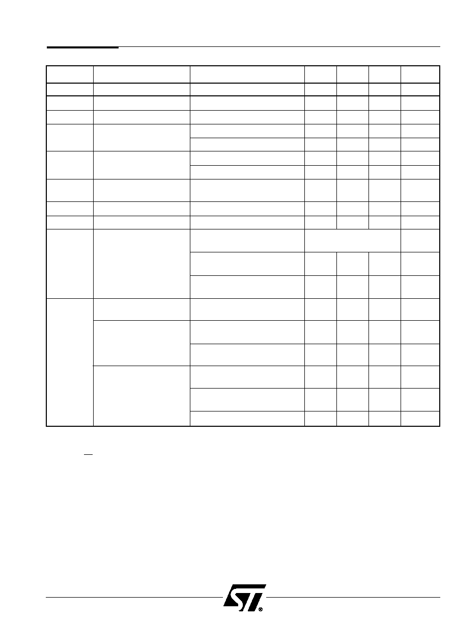
PSD3XX Family
39
Symbol
Parameter
Conditions
Min
Typ
Max
Unit
V
CC
Supply Voltage
All Speeds
2.7
3
5.5
V
V
IH
High-Level Input Voltage
2.7 V < V
CC
> 5.5 V
.7 V
CC
V
CC
+ .5
V
V
IL
Low-Level Input Voltage
2.7 V < V
CC
> 5.5 V
≠ 0.5
.3 V
CC
V
I
OH
= ≠ 20 µA, V
CC
= 2.7 V
2.6
2.69
V
V
OH
Output High Voltage
I
OH
= ≠ 1 mA, V
CC
= 2.7 V
2.3
2.4
V
I
OL
= 20 µA, V
CC
= 2.7 V
0.01
0.1
V
V
OL
Output Low Voltage
I
OL
= 4 mA, V
CC
= 2.7 V
0.15
0.45
V
I
SB
Standby Supply Current
V
CC
= 3.0 V
1
5
µA
(Notes 1,4)
I
LI
Input Leakage Current
V
IN
= V
CC
or GND
≠1
±.1
1
µA
I
LO
Output Leakage Current
V
OUT
= V
CC
or GND
≠1
.1
1
µA
ZPLD Turbo Mode = Off,
f = 0 MHz, V
CC
= 3.0 V
See I
SB
µA
I
CC
(DC)
Operating Supply Current
ZPLD Turbo Mode = On,
(Note 3)
f = 0 MHz, V
CC
= 3.0 V
0.17
0.35
mA/PT
EPROM, f = 0 MHz,
V
CC
= 3.0 V
0
0
µA
ZPLD AC Base
See Figure 15 (V
CC
= 3.0 V)
See
0.5
mZ/MHz
Fig. 15
CMiser = On and 8-Bit Bus
EPROM Access
Mode (V
CC
= 3.0 V)
0.4
1
mA/MHz
AC Adder
All Other Cases (Note 5)
I
CC
(AC)
(V
CC
= 3.0 V)
0.9
1.7
mA/MHz
(Note 3)
CMiser = On and 8-Bit Bus
0.7
1.4
mA/MHz
Mode (V
CC
= 3.0 V)
SRAM Access AC Adder
CMiser = On and 16-Bit Bus
1
2
mA/MHz
Mode (V
CC
= 3.0 V)
CMiser = Off (V
CC
= 3.0 V)
1.9
3.8
mA/MHz
18.6 AC/DC DC Characteristics ≠ ZPSD3XXV (3 V devices only)
NOTES: 1. CMOS inputs: GND ± 0.3 V or V
CC
± 0.3V.
2. TTL inputs: V
IL
0.8 V, V
IH
2.0 V.
3. I
OUT
= 0 mA.
4. CSI/A19 is high and the part is in a power-down configuration mode.
5. All other cases include CMiser = On and 16-bit bus mode and CMiser = Off and 8- or 16-bit bus mode.
PSD3XX Family
40
-70
-90*
-15
CMiser Turbo
Symbol
Parameter
On =
Off =
Unit
Min
Max
Min
Max
Min
Max
Add
Add
T1
ALE or AS Pulse Width
18
20
40
0
0
ns
T2
Address Set-up Time
5
5
12
0
0
ns
T3
Address Hold Time
7
8
10
0
0
ns
T4
Leading Edge of Read
to Data Active
0
0
0
0
0
ns
T5
ALE Valid to Data Valid
80
100
160
10
0
ns
T6
Address Valid to Data Valid
70
90
150
10
0
ns
T7
CSI Active to Data Valid
80
100
160
10
0
ns
T8
Leading Edge of Read
to Data Valid
20
32
55
0
0
ns
Leading Edge of Read to
Data Valid in 8031-Based
T8A
Architecture Operating with
32
32
55
0
0
ns
PSEN and RD in Separate
Mode
T9
Read Data Hold Time
0
0
0
0
0
ns
T10
Trailing Edge of Read to
Data High-Z
20
32
35
0
0
ns
Trailing Edge of ALE or AS
T11
to Leading Edge of Write
0
0
0
0
0
ns
T12
RD, E, PSEN, or DS Pulse Width
35
40
60
0
0
ns
T12A
WR Pulse Width
18
20
35
0
0
ns
Trailing Edge of Write or Read
T13
to Leading Edge of ALE or AS
5
5
5
0
0
ns
T14
Address Valid to Trailing Edge
of Write
70
90
150
0
0
ns
CSI Active to Trailing Edge
T15
of Write
80
100
160
0
0
ns
T16
Write Data Set-up Time
18
20
30
0
0
ns
T17
Write Data Hold Time
5
5
10
0
0
ns
T18
Port to Data Out Valid
Propagation Delay
25
30
35
0
0
ns
T19
Port Input Hold Time
0
0
0
0
0
ns
T20
Trailing Edge of Write to Port
Output Valid
30
40
50
0
0
ns
T21
ADi
1
or Control to CSOi
2
Valid
6
20
6
25
6
35
0
10
ns
T22
ADi
1
or Control to CSOi
2
Invalid
5
20
5
25
4
35
0
10
ns
18.7 Timing Parameters ≠ PSD3XX/ZPSD3XX (All 5 V devices)
*
-90 speed available only on Industrial Temperature versions.
PSD3XX Family
41
-70
-90*
-15
CMiser Turbo
Symbol
Parameter
On =
Off =
Unit
Min
Max
Min
Max
Min
Max
Add
Add
Track Mode Address
Propagation Delay:
22
22
28
0
0
ns
T23
CSADOUT1 Already True
Latched Address Outputs,
Port A
22
22
28
0
0
Track Mode Address
Propagation Delay:
T23A
CSADOUT1 Becomes True
33
33
50
0
10
ns
During ALE or AS
Track Mode Trailing Edge of
T24
ALE or AS to Address High-Z
30
32
35
0
0
ns
T25
Track Mode Read Propagation
Delay
27
29
35
0
0
ns
T26
Track Mode Read Hold Time
5
29
11
29
11
29
0
0
ns
T27
Track Mode Write Cycle,
Data Propagation Delay
18
20
30
0
0
ns
Track Mode Write Cycle,
T28
Write to Data Propagation Delay
6
30
8
30
9
40
0
10
ns
Hold Time of Port A Valid
T29
During Write CSOi
2
Trailing Edge
2
2
2
0
0
ns
T30
CSI Active to CSOi
2
Active
8
37
9
40
9
50
0
0
ns
T31
CSI Inactive to CSOi
2
Inactive
8
37
9
40
9
50
0
0
ns
T32
Direct PAD Input
3
as Hold Time
0
10
12
0
0
ns
T33
R/W Active to E or DS Start
18
20
30
0
0
ns
T34
E or DS End to R/W
18
20
30
0
0
ns
T35
AS Inactive to E high
0
0
0
0
0
ns
T36
Address to Leading Edge
of Write
18
20
25
0
0
ns
18.7 Timing Parameters ≠ PSD3XX/ZPSD3XX (All 5 V devices)
(cont.)
NOTES:
1. ADi = any address line.
2. CSOi = any of the chip-select output signals coming through Port B (CS0≠CS7) or through Port C (CS8≠CS10).
3. Direct PAD input = any of the following direct PAD input lines: CSI/A19 as transparent A19, RD/E/DS, WR or
R/W, transparent PC0≠PC2, ALE (or AS).
4. Control signals RD/E/DS or WR or R/W.
*
-90 speed available only on Industrial Temperature versions.
PSD3XX Family
42
-15*
-20
-25
CMiser Turbo
Symbol
Parameter
On =
Off =
Unit
Min
Max
Min
Max
Min
Max
Add
Add
T1
ALE or AS Pulse Width
40
50
60
0
0
ns
T2
Address Set-up Time
12
15
20
0
0
ns
T3
Address Hold Time
10
15
20
0
0
ns
T4
Leading Edge of Read
to Data Active
0
0
0
0
0
ns
T5
ALE Valid to Data Valid
170
200
250
20
0
ns
T6
Address Valid to Data Valid
150
200
250
20
0
ns
T7
CSI Active to Data Valid
160
200
250
20
0
ns
T8
Leading Edge of Read
to Data Valid
45
50
60
0
0
ns
Leading Edge of Read to
Data Valid in 8031-Based
T8A
Architecture Operating with
65
70
80
0
0
ns
PSEN and RD in Separate
Mode
T9
Read Data Hold Time
0
0
0
0
0
ns
T10
Trailing Edge of Read to
Data High-Z
45
50
55
0
0
ns
Trailing Edge of ALE or AS
T11
to Leading Edge of Write
0
0
0
0
0
ns
T12
RD, E, PSEN, or DS Pulse Width
60
75
85
0
0
ns
T12A
WR Pulse Width
35
45
55
0
0
ns
Trailing Edge of Write or Read
T13
to Leading Edge of ALE or AS
5
5
5
0
0
ns
T14
Address Valid to Trailing Edge
of Write
150
200
250
0
0
ns
CSI Active to Trailing Edge
T15
of Write
160
200
250
0
0
ns
T16
Write Data Set-up Time
30
40
50
0
0
ns
T17
Write Data Hold Time
10
12
15
0
0
ns
T18
Port to Data Out Valid
Propagation Delay
45
50
60
0
0
ns
T19
Port Input Hold Time
0
0
0
0
0
ns
T20
Trailing Edge of Write to Port
Output Valid
50
60
70
0
0
ns
T21
ADi
1
or Control to CSOi
2
Valid
6
50
5
55
5
60
0
20
ns
T22
ADi
1
or Control to CSOi
2
Invalid
4
50
4
55
4
60
0
20
ns
18.8 Timing Parameters ≠ ZPSD3XXV (3 V devices only)
*
-15 speed available only on ZPSD311V.
PSD3XX Family
43
NOTES:
1. ADi = any address line.
2. CSOi = any of the chip-select output signals coming through Port B (CS0≠CS7) or through Port C (CS8≠CS10).
3. Direct PAD input = any of the following direct PAD input lines: CSI/A19 as transparent A19, RD/E/DS, WR or
R/W, transparent PC0≠PC2, ALE (or AS).
4. Control signals RD/E/DS or WR or R/W.
*
-15 speed available only on ZPSD311V.
-15*
-20
-25
CMiser Turbo
Symbol
Parameter
On =
Off =
Unit
Min
Max
Min
Max
Min
Max
Add
Add
Track Mode Address
Propagation Delay:
50
60
60
0
0
ns
T23
CSADOUT1 Already True
Latched Address Outputs,
Port A
50
60
60
0
0
Track Mode Address
Propagation Delay:
T23A
CSADOUT1 Becomes True
70
80
90
0
20
ns
During ALE or AS
Track Mode Trailing Edge of
T24
ALE or AS to Address High-Z
50
60
60
0
0
ns
T25
Track Mode Read Propagation
Delay
45
55
60
0
0
ns
T26
Track Mode Read Hold Time
10
70
10
70
10
70
0
0
ns
T27
Track Mode Write Cycle,
Data Propagation Delay
45
55
60
0
0
ns
Track Mode Write Cycle,
T28
Write to Data Propagation Delay
8
65
8
75
8
80
0
20
ns
Hold Time of Port A Valid
T29
During Write CSOi
2
Trailing Edge
2
3
3
0
0
ns
T30
CSI Active to CSOi
2
Active
9
70
9
80
9
90
0
0
ns
T31
CSI Inactive to CSOi
2
Inactive
9
70
9
80
9
90
0
0
ns
T32
Direct PAD Input
3
as Hold Time
0
0
0
0
0
ns
T33
R/W Active to E or DS Start
30
40
50
0
0
ns
T34
E or DS End to R/W
30
40
50
0
0
ns
T35
AS Inactive to E high
0
0
0
0
0
ns
T36
Address to Leading Edge
of Write
30
35
40
0
0
ns
18.8 Timing Parameters ≠ ZPSD3XXV (3 V devices only)
(cont.)
18.9 Timing Diagrams for all PSD3XX Parts
Figure 20. Timing of 8-Bit Multiplexed Address/Data Bus Using RD, WR (PSD3X1)
18
DATA VALID
CSI/A19
as CSI
DATA
IN
8
12
1
7
15
32
32
14
14
6
6
10
9
ADDRESS A
ADDRESS B
2
3
4
13
32
5
2
16
17
12A
19
13
20
23
23
ADDRESS A
ADDRESS B
INPUT
INPUT
OUTPUT
OUTPUT
READ CYCLE
WRITE CYCLE
STABLE INPUT
STABLE INPUT
Direct
(1)
PAD Input
Multiplexed
(2)
Inputs
A0/AD0-
A7/AD7
Active Low
ALE
Active High
ALE
RD/E as RD
BHE/PSEN
as PSEN
WR/V
PP
or
RW as WR
Any of
PA0-PA7
as I/O Pin
Any of
PA0-PA7 Pins
as Address
Outputs
Any of
PB0-PB7
as I/O Pin
1
3
11
36
See referenced notes on page 64.
PSD3XX Family
44
PSD3XX Family
45
Figure 21. Timing of 8-Bit Multiplexed Address/Data Bus Using RD, WR (PSD3X2/3X3)
18
DATA VALID
CSI/A19
as CSI
DATA
IN
8
12
1
7
15
32
32
14
14
6
6
10
9
ADDRESS A
ADDRESS B
2
3
4
13
32
5
2
16
17
12A
19
13
20
23
23
ADDRESS A
ADDRESS B
INPUT
INPUT
OUTPUT
OUTPUT
READ CYCLE
WRITE CYCLE
STABLE INPUT
STABLE INPUT
Direct
(1)
PAD Input
Multiplexed
(2)
Inputs
A0/AD0-
A7/AD7
Active Low
ALE
Active High
ALE
RD/E/DS as RD
BHE/PSEN
as PSEN
WR/V
PP
or
RW as WR
Any of
PA0-PA7
as I/O Pin
Any of
PA0-PA7 Pins
as Address
Outputs
Any of
PB0-PB7
as I/O Pin
1
3
11
36
See referenced notes on page 64
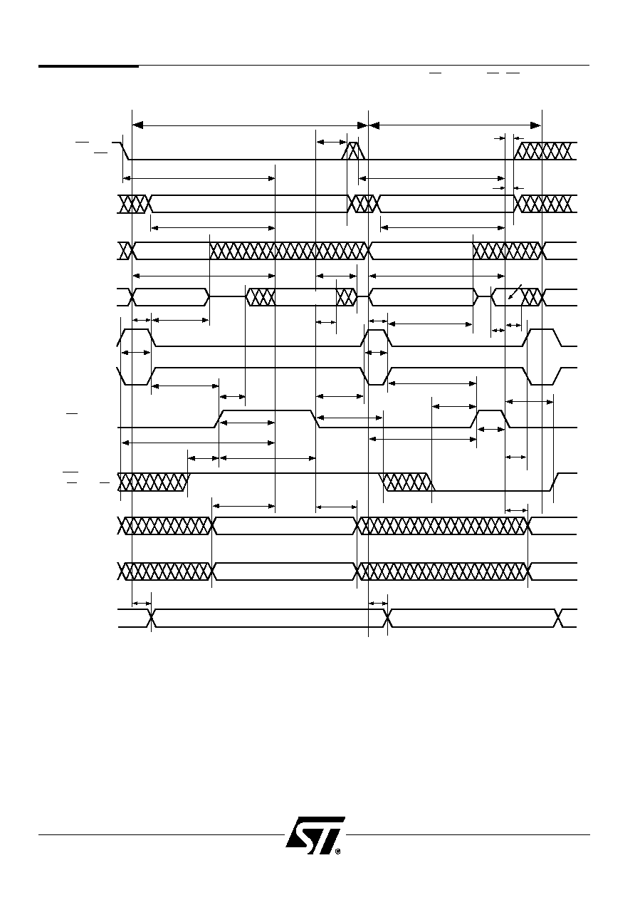
PSD3XX Family
46
Figure 22. Timing of 8-Bit Multiplexed Address/Data Bus Using R/W, E or R/W, DS (PSD3X1)
18
33
34
36
19
DATA VALID
CSI/A19
as CSI
DATA
IN
8
12
5
1
32
7
15
32
32
14
14
6
6
10
9
ADDRESS A
ADDRESS B
2
3
4
33
13
2
16
17
12
13
20
23
23
ADDRESS A
ADDRESS B
INPUT
INPUT
OUTPUT
OUTPUT
READ CYCLE
WRITE CYCLE
STABLE INPUT
STABLE INPUT
Direct
(1)
PAD Input
Multiplexed
(2)
Inputs
A0/AD0-
A7/AD7
Active Low
AS
Active High
AS
RD/E as E
WR/V
PP
or
R/W as R/W
Any of
PA0-PA7
as I/O Pin
Any of
PA0-PA7 Pins
as Address
Outputs
Any of
PB0-PB7
as I/O Pin
1
3
34
35
35
See referenced notes on page 64.

PSD3XX Family
47
Figure 23. Timing of 8-Bit Multiplexed Address/Data Bus Using R/W E or R/W, DS
(PSD3X2/3X3)
18
33
34
36
19
DATA VALID
CSI/A19
as CSI
DATA
IN
8
12
5
1
32
7
15
32
32
14
14
6
6
10
9
ADDRESS A
ADDRESS B
2
3
4
33
13
2
16
17
12
13
20
23
23
ADDRESS A
ADDRESS B
INPUT
INPUT
OUTPUT
OUTPUT
READ CYCLE
WRITE CYCLE
STABLE INPUT
STABLE INPUT
Direct
(1)
PAD Input
Multiplexed
(2)
Inputs
A0/AD0-
A7/AD7
Active Low
AS
Active High
AS
RD/E/DS as E
WR/V
PP
or
R/W as R/W
Any of
PA0-PA7
as I/O Pin
Any of
PA0-PA7 Pins
as Address
Outputs
Any of
PB0-PB7
as I/O Pin
1
3
34
35
RD/E/DS as DS
35
See referenced notes on page 64.
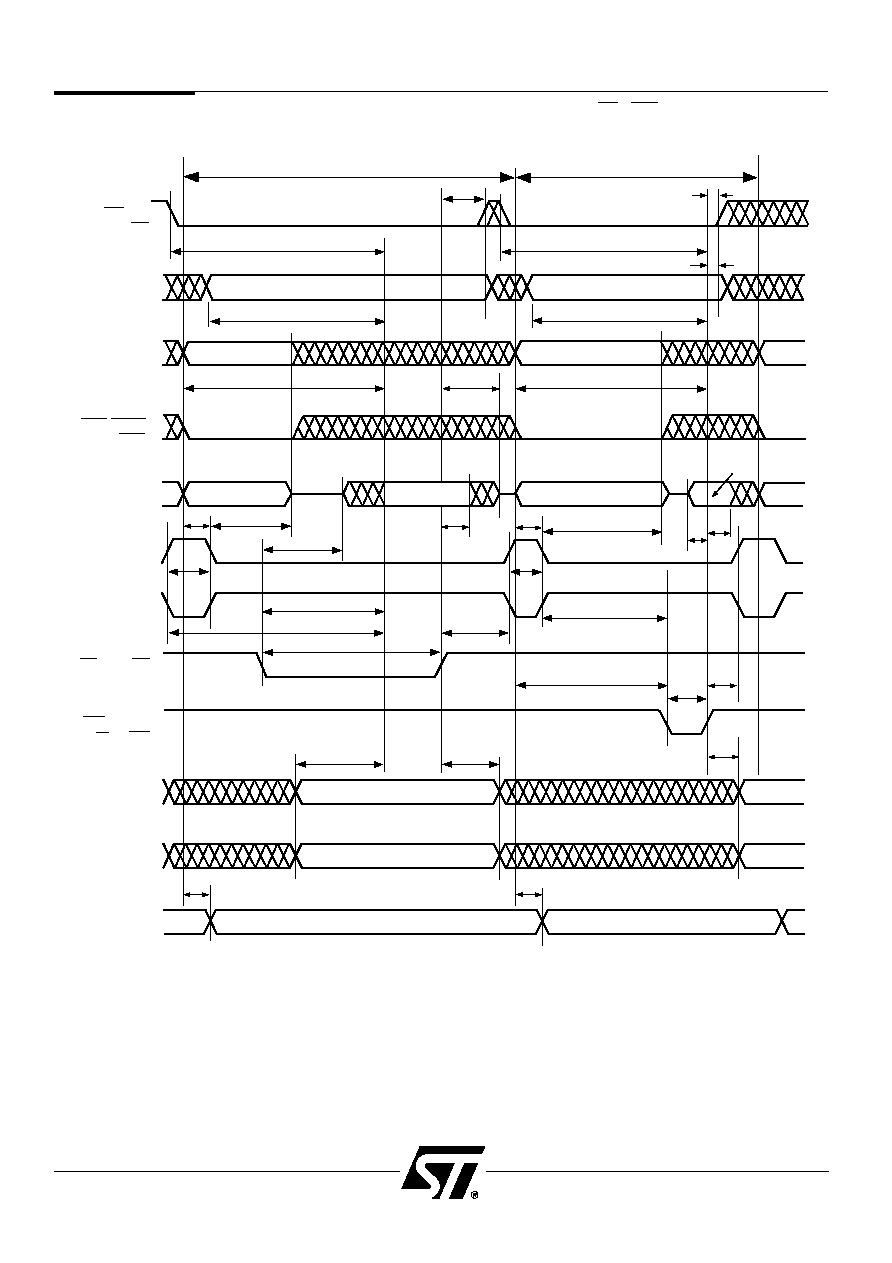
PSD3XX Family
48
Figure 24. Timing of 16-Bit Multiplexed Address/Data Bus Using RD, WR (PSD3X1)
18
36
4
19
DATA VALID
CSI/A19
as CSI
12
5
1
7
15
32
32
14
14
6
6
10
9
ADDRESS A
ADDRESS B
2
3
8
13
2
16
17
12A
13
20
23
23
ADDRESS A
ADDRESS B
INPUT
INPUT
OUTPUT
OUTPUT
READ CYCLE
WRITE CYCLE
STABLE INPUT
STABLE INPUT
Direct
(1)
PAD Input
Multiplexed
(2)
Inputs
DATA
IN
A0/AD0-
A15/AD15
Active Low
ALE
Active High
ALE
RD/E as RD
BHE/PSEN
as BHE
Any of
PA0-PA7
as I/O Pin
Any of
PA0-PA7 Pins
as Address
Outputs
Any of
PB0-PB7
as I/O Pin
1
3
11
WR/V
PP
or
R/W as WR
32
See referenced notes on page 64.
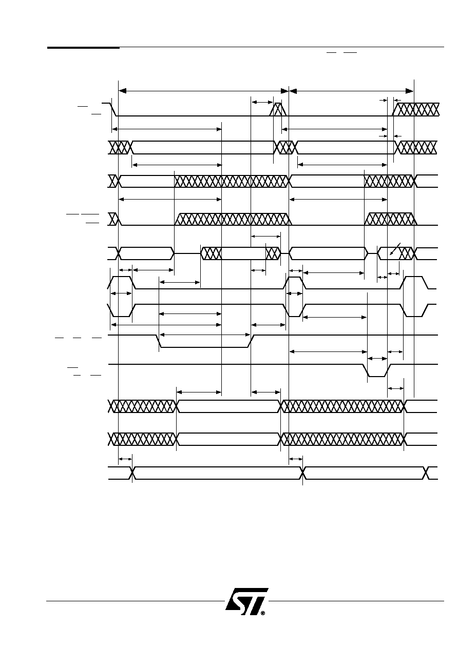
PSD3XX Family
49
Figure 25. Timing of 16-Bit Multiplexed Address/Data Bus Using RD, WR (PSD3X2/3X3)
18
36
4
19
DATA VALID
CSI/A19
as CSI
12
5
1
7
15
32
32
14
14
6
6
10
9
ADDRESS A
ADDRESS B
2
3
8
13
2
16
17
12A
13
20
23
23
ADDRESS A
ADDRESS B
INPUT
INPUT
OUTPUT
OUTPUT
READ CYCLE
WRITE CYCLE
STABLE INPUT
STABLE INPUT
Direct
(1)
PAD Input
Multiplexed
(2)
Inputs
DATA
IN
A0/AD0-
A15/AD15
Active Low
ALE
Active High
ALE
RD/E/DS as RD
BHE/PSEN
as BHE
Any of
PA0-PA7
as I/O Pin
Any of
PA0-PA7 Pins
as Address
Outputs
Any of
PB0-PB7
as I/O Pin
1
3
11
WR/V
PP
or
R/W as WR
32
See referenced notes on page 64.
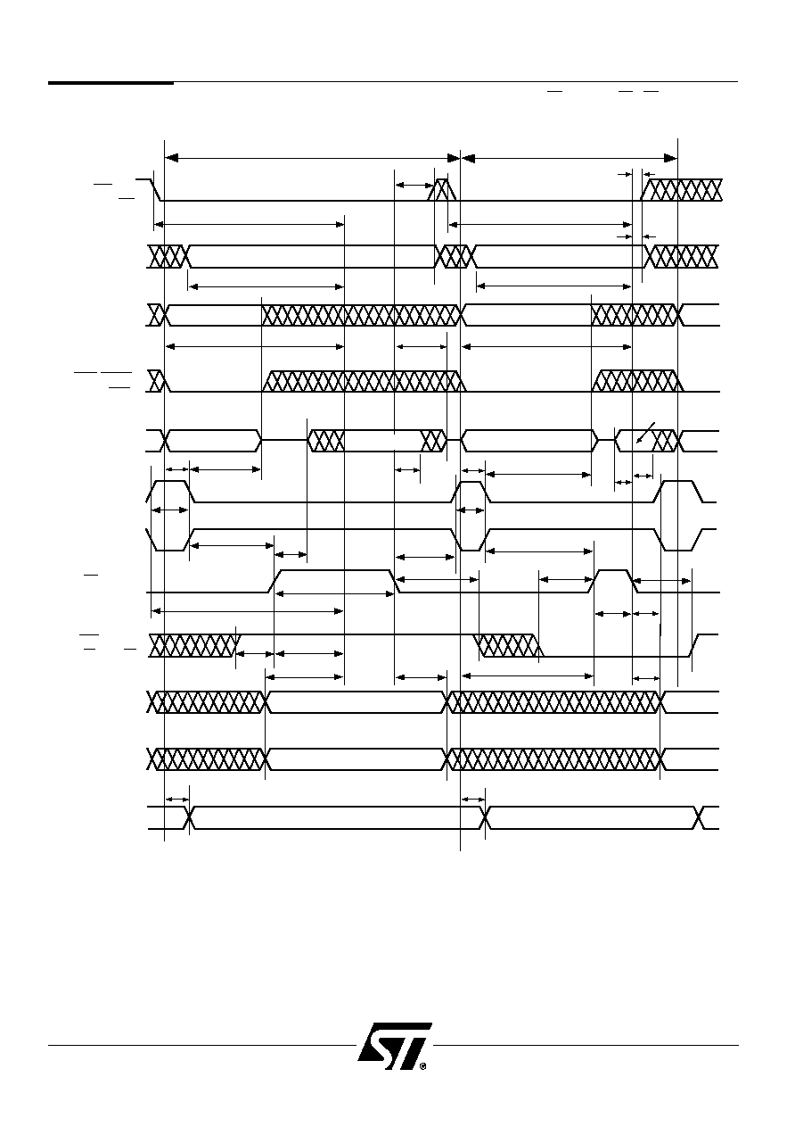
PSD3XX Family
50
Figure 26. Timing of 16-Bit Multiplexed Address/Data Bus Using R/W, E or R/W, DS (PSD3X1)
18
19
33
DATA VALID
CSI/A19
as CSI
1
32
7
15
32
32
14
14
6
6
10
9
ADDRESS A
ADDRESS B
2
3
35
13
4
2
16
17
20
23
23
ADDRESS A
ADDRESS B
INPUT
INPUT
OUTPUT
OUTPUT
READ CYCLE
WRITE CYCLE
STABLE INPUT
STABLE INPUT
Direct
(1)
PAD Input
Multiplexed
(2)
Inputs
DATA
IN
A0/AD0-
A15/AD15
Active Low
AS
Active High
AS
BHE/PSEN
as BHE
Any of
PA0-PA7
as I/O Pin
Any of
PA0-PA7 Pins
as Address
Outputs
Any of
PB0-PB7
as I/O Pin
1
3
35
34
34
33
8
12
5
12
13
as E
RD/E as E
as E
WR/V
PP
or
R/W as R/W
36
See referenced notes on page 64.
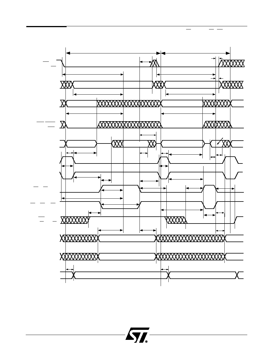
PSD3XX Family
51
Figure 27. Timing of 16-Bit Multiplexed Address/Data Bus Using R/W, E or R/W, DS
(PSD3X2/3X3)
18
19
33
DATA VALID
CSI/A19
as CSI
1
32
7
15
32
32
14
14
6
6
10
9
ADDRESS A
ADDRESS B
2
3
35
13
4
2
16
17
20
23
23
ADDRESS A
ADDRESS B
INPUT
INPUT
OUTPUT
OUTPUT
READ CYCLE
WRITE CYCLE
STABLE INPUT
STABLE INPUT
Direct
(1)
PAD Input
Multiplexed
(2)
Inputs
DATA
IN
A0/AD0-
A15/AD15
Active Low
AS
Active High
AS
BHE/PSEN
as BHE
Any of
PA0-PA7
as I/O Pin
Any of
PA0-PA7 Pins
as Address
Outputs
Any of
PB0-PB7
as I/O Pin
1
3
35
34
34
33
8
12
5
12
13
RD/E/DS as E
RD/E/DS as E
RD/E/DS as E
RD/E/DS as E
WR/V
PP
or
R/W as R/W
RD/E/DS as DS
36
See referenced notes on page 64.
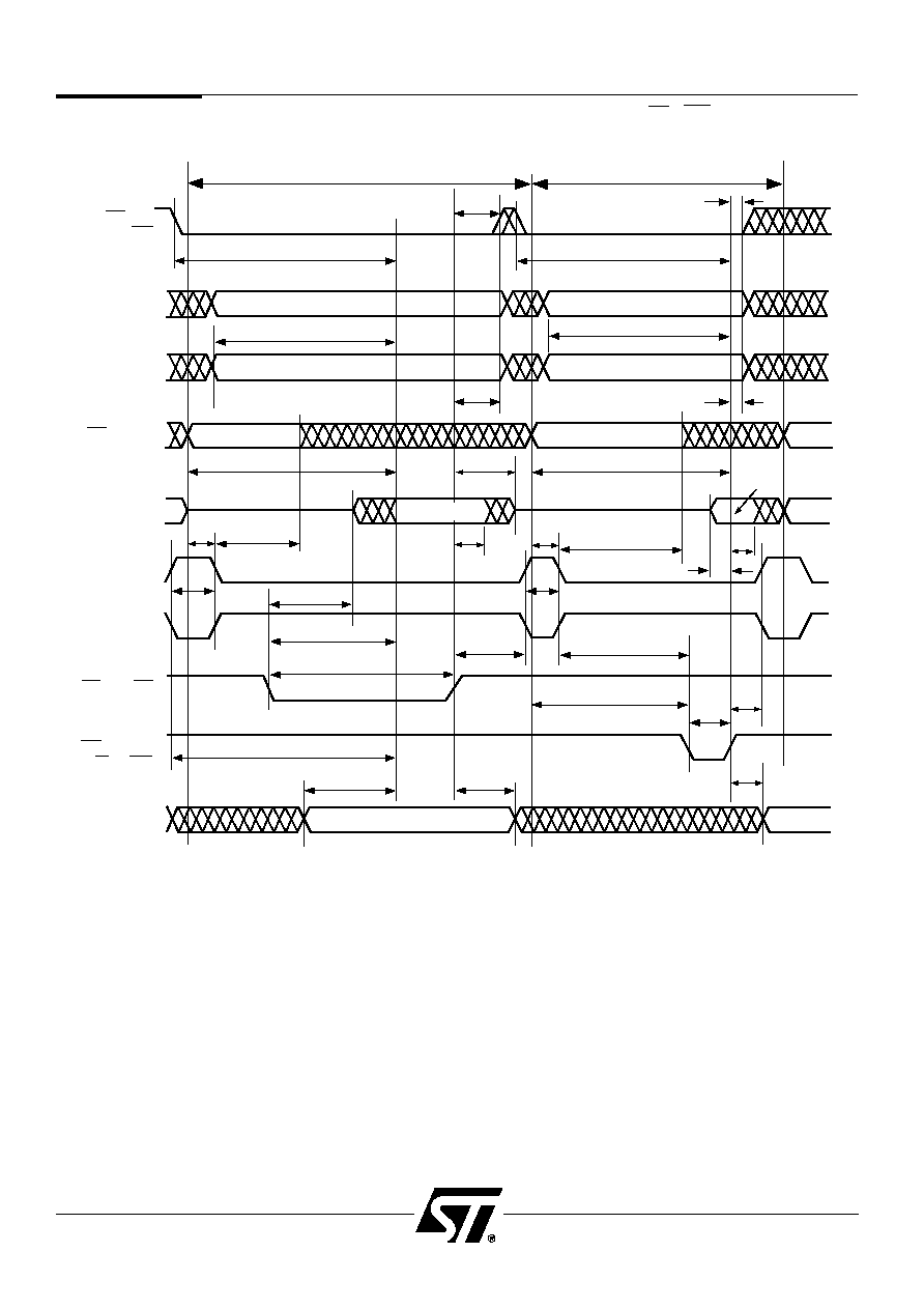
PSD3XX Family
52
Figure 28. Timing of 8-Bit Non-Multiplexed Address/Data Bus Using RD, WR (PSD3X1)
18
8
19
DATA VALID
CSI/A19
as CSI
12
5
1
7
15
32
14
14
6
6
10
9
2
3
4
32
13
2
16
17
12A
13
20
INPUT
OUTPUT
READ CYCLE
WRITE CYCLE
STABLE INPUT
STABLE INPUT
A0/AD0-
A15/AD15
as A0-A15
STABLE INPUT
STABLE INPUT
Direct
(1)
PAD Input
PC0-PC2,
CSI/A19 as
Multiplexed
Inputs
DATA
IN
PA0-PA7
Active Low
ALE
Active High
ALE
RD/E as RD
Any of
PB0-PB7
as I/O Pin
1
3
11
32
32
WR/VPP or
R/W as WR
36
See referenced notes on page 64.

PSD3XX Family
53
Figure 29. Timing of 8-Bit Non-Multiplexed Address/Data Bus Using RD, WR (PSD3X2/3X3)
18
8
19
DATA VALID
CSI/A19
as CSI
12
5
1
7
15
32
14
14
6
6
10
9
2
3
4
32
13
2
16
17
12A
13
20
INPUT
OUTPUT
READ CYCLE
WRITE CYCLE
STABLE INPUT
STABLE INPUT
A0/AD0-
A15/AD15
as A0-A15
STABLE INPUT
STABLE INPUT
Direct
(1)
PAD Input
Multiplexed
(2)
Inputs
DATA
IN
PA0-PA7
Active Low
ALE
Active High
ALE
RD/E/DS as RD
Any of
PB0-PB7
as I/O Pin
1
3
11
32
32
WR/VPP or
R/W as WR
36
See referenced notes on page 64.

PSD3XX Family
54
Figure 30. Timing of 8-Bit Non-Multiplexed Address/Data Bus Using R/W, E or R/W, DS
(PSD3X1)
8
DATA VALID
CSI/A19
as CSI
1
7
15
32
32
14
14
6
6
10
9
2
3
35
32
32
2
16
17
READ CYCLE
WRITE CYCLE
STABLE INPUT
STABLE INPUT
A0/AD0-
A15/AD15
as A0-A15
STABLE INPUT
STABLE INPUT
Direct
(1)
PAD Input
PC0-PC2,
CSI/A19 as
Multiplexed
Inputs
DATA
IN
PA0-PA7
Active Low
ALE
Active High
ALE
1
3
35
18
12
19
33
13
20
INPUT
OUTPUT
Any of
PB0-PB7
as I/O Pin
4
34
34
33
12
13
RD/E as E
as E
as E
as E
WR/V
PP
or
R/W as R/W
36
See referenced notes on page 64.

PSD3XX Family
55
Figure 31. Timing of 8-Bit Non-Multiplexed Address/Data Bus Using R/W, E or R/W, DS
(PSD3X2/3X3)
8
DATA VALID
CSI/A19
as CSI
1
7
15
32
32
14
14
6
6
10
9
2
3
35
32
32
2
16
17
READ CYCLE
WRITE CYCLE
STABLE INPUT
STABLE INPUT
A0/AD0-
A15/AD15
as A0-A15
STABLE INPUT
STABLE INPUT
Direct
(1)
PAD Input
Multiplexed
(2)
Inputs
DATA
IN
PA0-PA7
Active Low
ALE
Active High
ALE
1
3
35
36
18
19
33
13
20
INPUT
OUTPUT
Any of
PB0-PB7
as I/O Pin
4
34
34
33
12
5
12
13
RD/E/DS as E
RD/E/DS as E
RD/E/DS as E
RD/E/DS as E
WR/V
PP
or
R/W as R/W
RD/E/DS as DS
See referenced notes on page 64.

PSD3XX Family
56
Figure 32. Timing of 16-Bit Non-Multiplexed Address/Data Bus Using RD, WR (PSD3X1)
8
CSI/A19
as CSI
1
32
7
15
32
32
14
6
6
4
32
READ CYCLE
WRITE CYCLE
STABLE INPUT
STABLE INPUT
A0/AD0-
A15/AD15
as A0-A15
STABLE INPUT
STABLE INPUT
Direct
(1)
PAD Input
PC0-PC2,
CSI/A19 as
Multiplexed
Inputs
DATA
IN
Active Low
ALE
Active High
ALE
1
3
3
2
2
11
13
12
12A
13
RD/E as RD
WR/V
PP
or
R/W as WR
DATA VALID
14
10
9
9
PA0-PA7
(Low Byte)
DATA
IN
DATA VALID
17
16
PB0-PB7
(High Byte)
BHE/PSEN
as BHE
36
See referenced notes on page 64.

PSD3XX Family
57
Figure 33. Timing of 16-Bit Non-Multiplexed Address/Data Bus Using RD, WR (PSD3X2/3X3)
8
CSI/A19
as CSI
1
32
7
15
32
32
14
6
6
4
32
READ CYCLE
WRITE CYCLE
STABLE INPUT
STABLE INPUT
A0/AD0-
A15/AD15
as A0-A15
STABLE INPUT
STABLE INPUT
Direct
(1)
PAD Input
Multiplexed
(2)
Inputs
DATA
IN
Active Low
ALE
Active High
ALE
1
3
3
2
2
11
13
12
5
12A
13
RD/E/DS as RD
WR/V
PP
or
R/W as WR
DATA VALID
14
10
9
PA0-PA7
(Low Byte)
DATA
IN
DATA VALID
17
16
PB0-PB7
(High Byte)
BHE/PSEN
as BHE
36
See referenced notes on page 64.
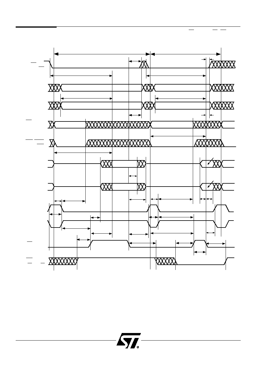
PSD3XX Family
58
Figure 34. Timing of 16-Bit Non-Multiplexed Address/Data Bus Using R/W, E or R/W, DS
(PSD3X1)
CSI/A19
as CSI
1
32
7
15
32
32
14
6
6
4
35
32
READ CYCLE
WRITE CYCLE
STABLE INPUT
STABLE INPUT
A0/AD0-
A15/AD15
as A0-A15
STABLE INPUT
STABLE INPUT
Direct
(1)
PAD Input
PC0-PC2,
CSI/A19 as
Multiplexed
Inputs
DATA
IN
Active Low
AS
Active High
AS
1
3
3
8
2
2
35
33
DATA VALID
14
10
9
PA0-PA7
(Low Byte)
DATA
IN
DATA VALID
17
16
PB0-PB7
(High Byte)
BHE/PSEN
as BHE
13
34
34
33
12
13
RD/E as E
as E
as E
as E
WR/V
PP
or
R/W as R/W
36
See referenced notes on page 64.
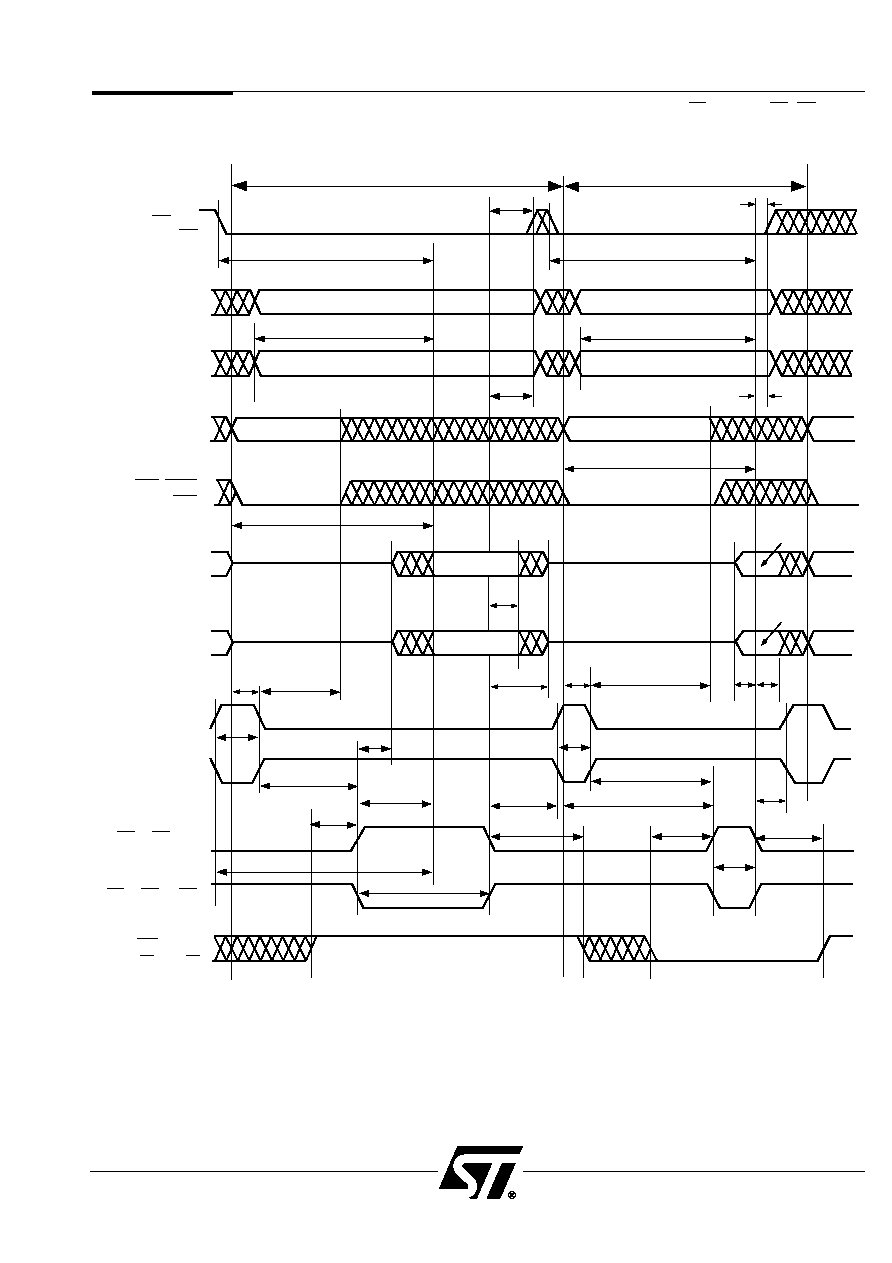
PSD3XX Family
59
Figure 35. Timing of 16-Bit Non-Multiplexed Address/Data Bus Using R/W, E or R/W, DS
(PSD3X2/3X3)
CSI/A19
as CSI
1
32
7
15
32
32
14
6
6
4
35
32
READ CYCLE
WRITE CYCLE
STABLE INPUT
STABLE INPUT
A0/AD0-
A15/AD15
as A0-A15
STABLE INPUT
STABLE INPUT
Direct
(1)
PAD Input
Multiplexed
(2)
Inputs
DATA
IN
Active Low
AS
Active High
AS
1
3
3
8
2
2
35
33
DATA VALID
14
10
9
PA0-PA7
(Low Byte)
DATA
IN
DATA VALID
17
16
PB0-PB7
(High Byte)
BHE/PSEN
as BHE
13
34
34
33
12
5
12
13
RD/E/DS as E
RD/E/DS as E
RD/E/DS as E
RD/E/DS as E
WR/V
PP
or
R/W as R/W
RD/E/DS as DS
36
See referenced notes on page 64.
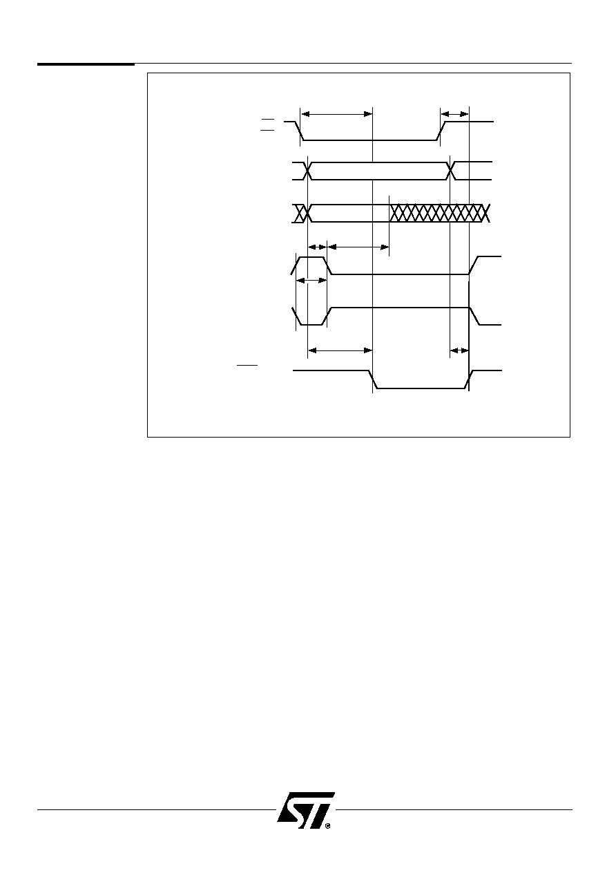
PSD3XX Family
60
Figure 36.
Chip-Select
Output Timing
30
21
31
A19/CSI
as CSI
Direct PAD
(1)
Input
Multiplexed
(2)
PAD Inputs
CSOi
(3,8)
ALE
(Multiplexed
Mode Only)
or ALE
(Multiplexed
Mode Only)
22
1
2
3
INPUT STABLE
See referenced notes on page 64.
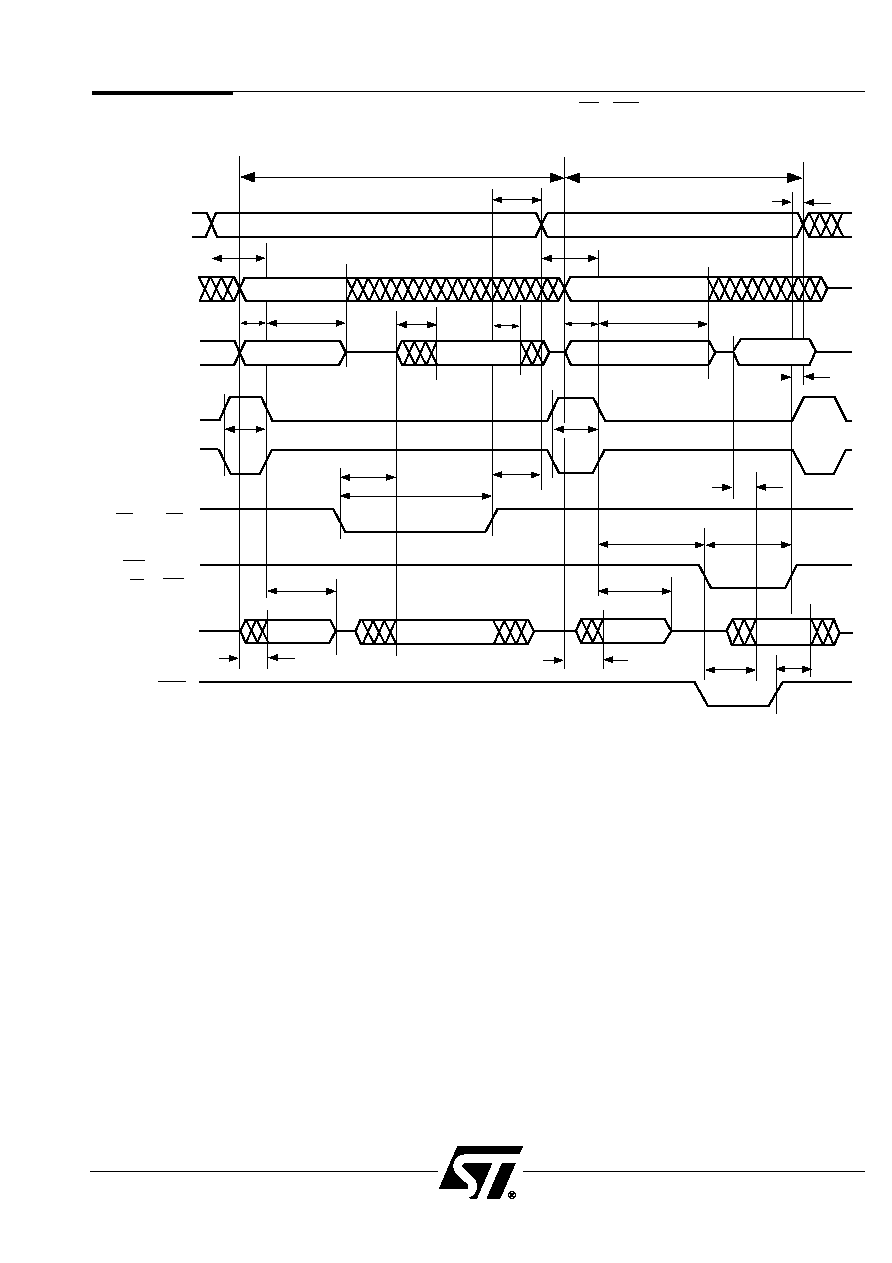
PSD3XX Family
61
Figure 37. Port A as AD0≠AD7 Timing (Track Mode) Using RD, WR (PSD3X1)
25
32
32
12A
28
24
11
DATA VALID
12
1
32
32
24
26
2
ADDRESS ADDRESS
2
3
2
2
4
READ CYCLE
WRITE CYCLE
STABLE INPUT
STABLE INPUT
STABLE INPUT
STABLE INPUT
Direct
PAD Input
(1,4)
Multiplexed
PAD Inputs
(5,7)
A0/AD0-
A7/AD7
or ALE
ALE
RD/E as RD
WR/V
PP
or
R/W as WR
1
3
27
PA0-PA7
29
CSOi
(3,6)
DATA IN
DATA
OUT
WRITTEN
DATA
23
ADR OUT
23
ADR OUT
See referenced notes on page 64.
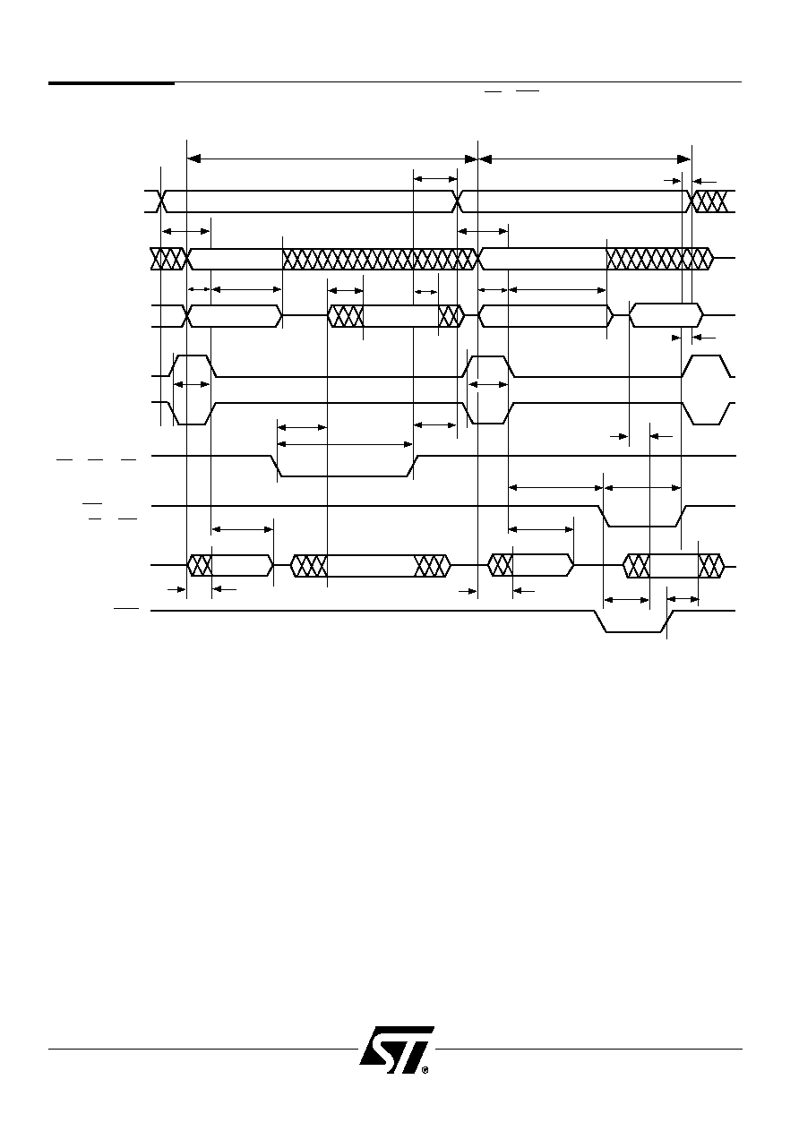
PSD3XX Family
62
Figure 38. Port A as AD0≠AD7 Timing (Track Mode) Using RD, WR (PSD3X2/3X3)
25
32
32
12A
28
24
11
DATA VALID
12
1
32
32
24
26
2
ADDRESS ADDRESS
2
3
2
2
4
READ CYCLE
WRITE CYCLE
STABLE INPUT
STABLE INPUT
STABLE INPUT
STABLE INPUT
Direct
PAD Input
(1,4)
Multiplexed
PAD Inputs
(5,7)
A0/AD0-
A7/AD7
or ALE
ALE
RD/E/DS as RD
WR/V
PP
or
R/W as WR
1
3
27
PA0-PA7
29
CSOi
(3,6)
DATA IN
DATA
OUT
WRITTEN
DATA
23
ADR OUT
23
ADR OUT
See referenced notes on page 64.
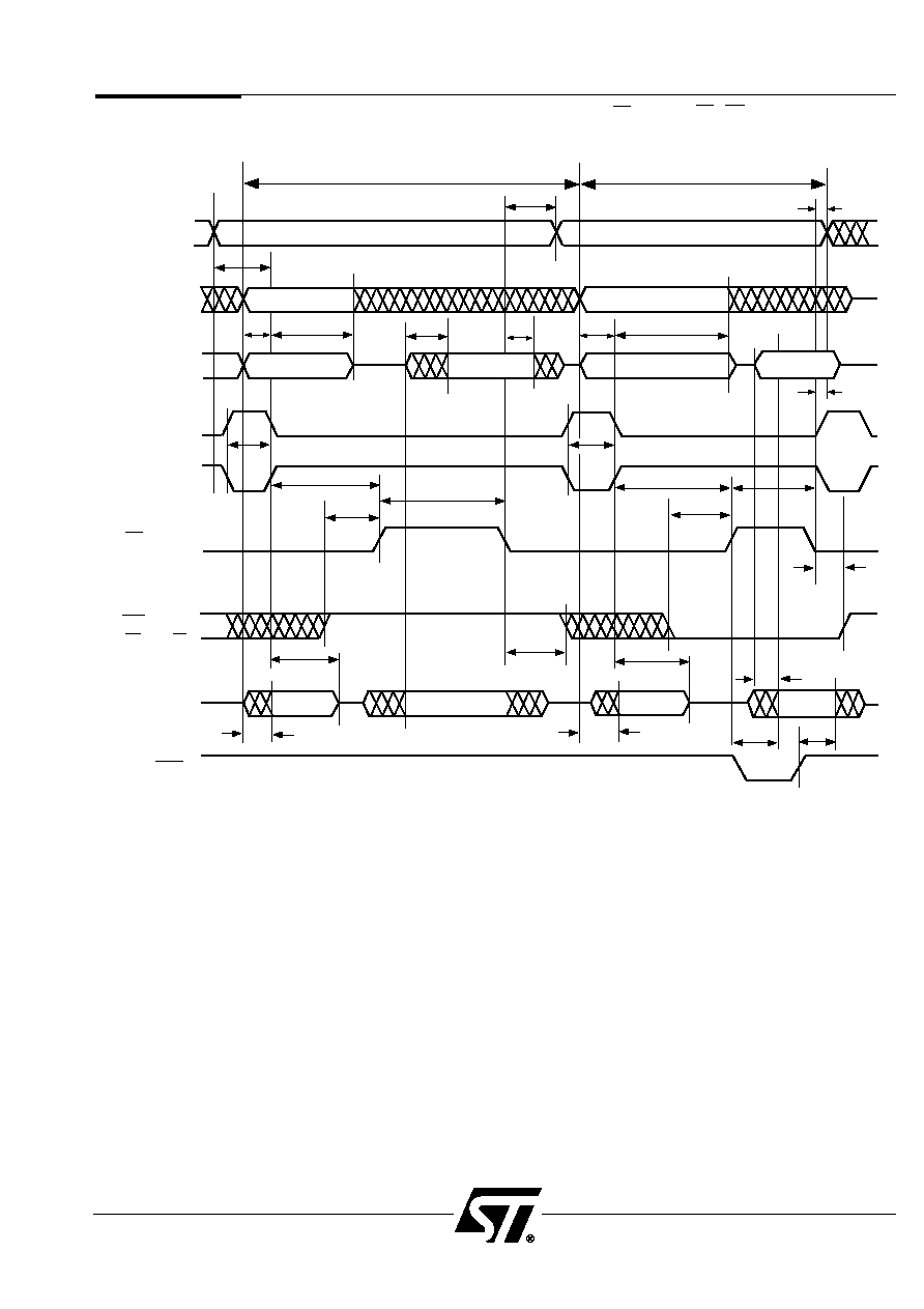
PSD3XX Family
63
Figure 39. Port A as AD0≠AD7 Timing (Track Mode) Using R/W, E or R/W, DS (PSD3X1)
33
25
33
32
12
28
24
34
35
DATA VALID
12
1
32
32
32
23
24
26
2
ADDRESS ADDRESS
2
3
2
35
READ CYCLE
WRITE CYCLE
STABLE INPUT
STABLE INPUT
STABLE INPUT
STABLE INPUT
Direct
PAD Input
(1,4)
Multiplexed
PAD Inputs
(5,7)
A0/AD0-
A7/AD7
or AS
AS
RD/E as E
as E
as E
as E
WR/V
PP
or
R/W as R/W
1
3
34
27
23
PA0-PA7
29
CSOi
(3,6)
ADR OUT
DATA IN
DATA
OUT
WRITTEN
DATA
ADR OUT
See referenced notes on page 64.
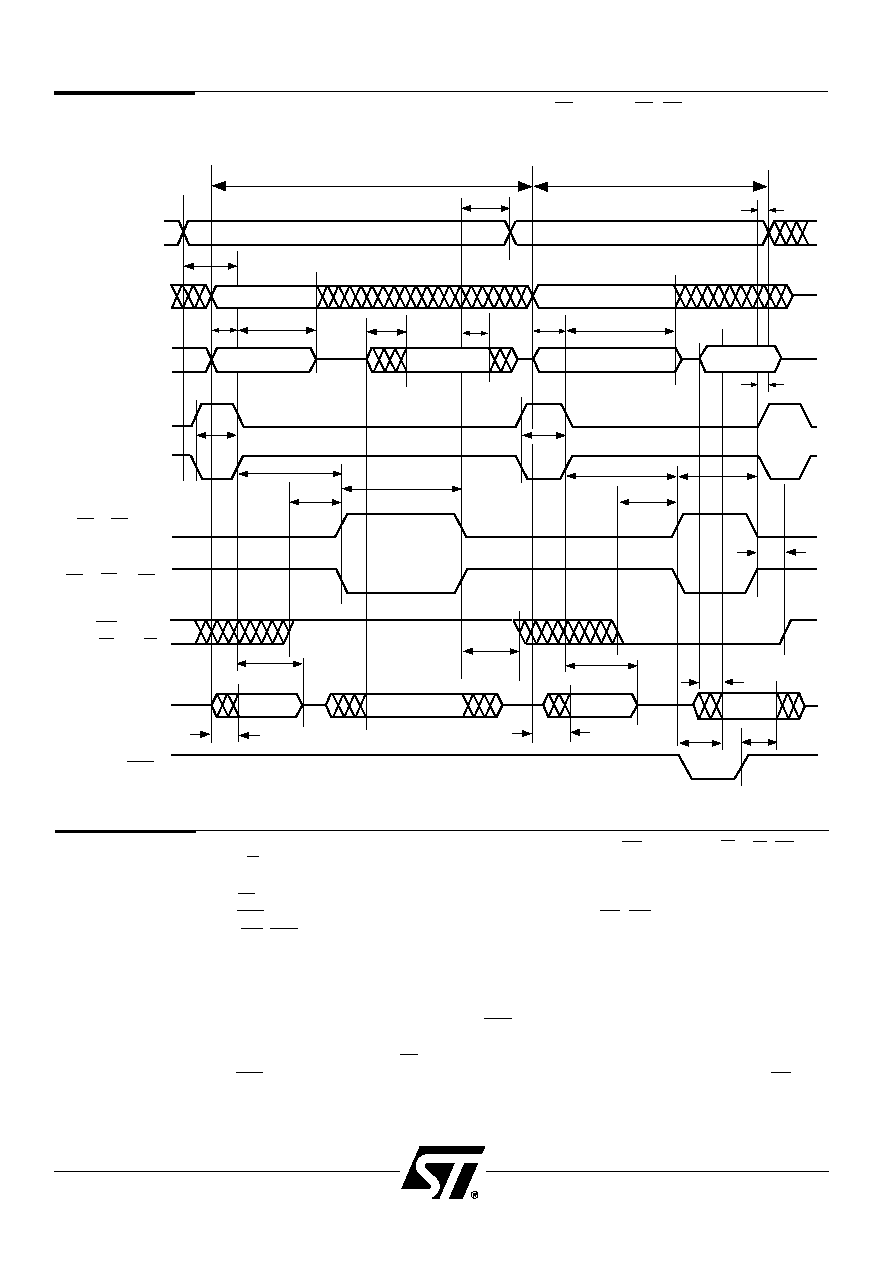
PSD3XX Family
64
Figure 40. Port A as AD0≠AD7 Timing (Track Mode) Using R/W, E or R/W, DS (PSD3X2/3X3)
33
25
33
32
12
28
24
34
35
DATA VALID
12
1
32
32
32
23
24
26
2
ADDRESS ADDRESS
2
3
2
35
READ CYCLE
WRITE CYCLE
STABLE INPUT
STABLE INPUT
STABLE INPUT
STABLE INPUT
Direct
PAD Input
(1,4)
Multiplexed
PAD Inputs
(5,7)
A0/AD0-
A7/AD7
or AS
AS
RD/E/DS as E
RD/E/DS as E
RD/E/DS as E
RD/E/DS as E
WR/V
PP
or
R/W as R/W
1
3
34
27
23
RD/E/DS as DS
PA0-PA7
29
CSOi
(3,6)
ADR OUT
DATA IN
DATA
OUT
WRITTEN
DATA
ADR OUT
1. Direct PAD input = any of the following direct PAD input lines: CSI/A19 as transparent A19, RD/E/DS, WR or
R/W, transparent PC0≠PC2, ALE in non-multiplexed modes.
2. Multiplexed inputs: any of the following inputs that are latched by the ALE (or AS): A0/AD0≠A15/AD15,
CSI/A19 as ALE dependent A19, ALE dependent PC0≠PC2.
3. CSOi = any of the chip-select output signals coming through Port B (CS0≠CS7) or through Port C
(CS8≠CS10).
4. CSADOUT1, which internally enables the address transfer to Port A, should be derived only from direct PAD
input signals, otherwise the address propagation delay is slowed down.
5. CSADIN and CSADOUT2, which internally enable the data-in or data-out transfers, respectively, can be
derived from any combination of direct PAD inputs and multiplexed PAD inputs.
6. The write operation signals are included in the CSOi expression.
7. Multiplexed PAD inputs: any of the following PAD inputs that are latched by the ALE (or AS) in the multiplexed
modes: A11/AD11≠A15/AD15, CSI/A19 as ALE dependent A19, ALE dependent PC0≠PC2.
8. CSOi product terms can include any of the PAD input signals shown in Figure 3, except for reset and CSI.
Notes for
Timing
Diagrams
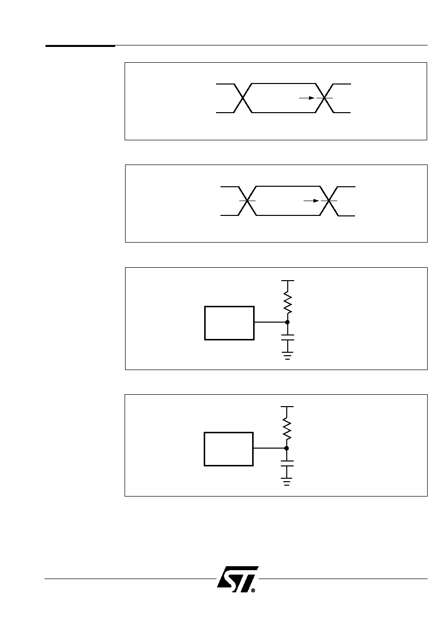
PSD3XX Family
65
Figure 41A. AC Testing Input/Output Waveform (5 V Versions)
Figure 41B. AC Testing Input/Output Waveform (3 V Versions)
3.0V
0V
TEST POINT
1.5V
DEVICE
UNDER TEST
2.01 V
195
C
L
= 30 pF
(INCLUDING
SCOPE AND JIG
CAPACITANCE)
0.9 V
CC
0V
TEST POINT
1.5V
Figure 42A. AC Testing Load Circuit (5 V Versions)
DEVICE
UNDER TEST
2.0 V
400
C
L
= 30 pF
(INCLUDING
SCOPE AND JIG
CAPACITANCE)
Figure 42B. AC Testing Load Circuit (3 V Versions)
18.10
AC Testing
PSD3XX Family
66
44-Pin
44-Pin
Pin Name
PLDCC/CLDCC
PQFP/TQFP
Package
Package
BHE/PSEN
1
39
WR/V
PP
or R/W
2
40
RESET
3
41
PB7
4
42
PB6
5
43
PB5
6
44
PB4
7
1
PB3
8
2
PB2
9
3
PB1
10
4
PB0
11
5
GND
12
6
ALE or AS
13
7
PA7
14
8
PA6
15
9
PA5
16
10
PA4
17
11
PA3
18
12
PA2
19
13
PA1
20
14
PA0
21
15
RD/E
22
16
AD0/A0
23
17
AD1/A1
24
18
AD2/A2
25
19
AD3/A3
26
20
AD4/A4
27
21
AD5/A5
28
22
AD6/A6
29
23
AD7/A7
30
24
AD8/A8
31
25
AD9/A9
32
26
AD10/A10
33
27
GND
34
28
AD11/A11
35
29
AD12/A12
36
30
AD13/A13
37
31
AD14/A14
38
32
AD15/A15
39
33
PC0
40
34
PC1
41
35
PC2
42
36
A19/CSI
43
37
V
CC
44
38
19.0
Pin
Assignments
PSD3XX Family
67
Figure 44.
Drawing M1 ≠
44 Pin Plastic Quad
Flatpack (PQFP)
(Package Type M)
OR
Drawing U1 ≠
44 Pin Plastic
Thin Quad Flatpack
(TQFP)
(Package Type U)
39 AD15/A15
38 AD14/A14
37 AD13/A13
36 AD12/A12
35 AD11/A11
34 GND
33 AD10/A10
32 AD9/A9
31 AD8/A8
30 AD7/A7
29 AD6/A6
PB4 7
PB3 8
PB2 9
PB1 10
PB0 11
GND 12
ALE or AS 13
PA7 14
PA6 15
PA5 16
PA4 17
PA3 18
PA2 19
PA1 20
PA0 21
RD/E 22
AD0/A0 23
AD1/A1 24
AD2/A2 25
AD3/A3 26
AD4/A4 27
AD5/A5 28
6 PB5
5 PB6
4 PB7
3 RESET
2 WR/V or R/W
1 BHE/PSEN
44 V
43 A19/CSI
42 PC2
41 PC1
40 PC0
PP
CC
PB4
PB3
PB2
PB1
PB0
GND
ALE or AS
PA7
PA6
PA5
PA4
AD15/A15
AD14/A14
AD13/A13
AD12/A12
AD11/A11
GND
AD10/A10
AD9/A9
AD8/A8
AD7/A7
AD6/A6
1
2
3
4
5
6
7
8
9
10
11
33
32
31
30
29
28
27
26
25
24
23
12
13
14
15
16
17
18
19
20
21
22
PA3
PA2
PA1
PA0
RD/E
AD0/A0
AD1/A1
AD2/A2
AD3/A3
AD4/A4
AD5/A5
PB5
PB6
PB7
RESET
WR/V
PP
or R/W
BHE/PSEN
V
CC
A19/CSI
PC2
PC1
PC0
44
43
42
41
40
39
38
37
36
35
34
(TOP VIEW)
20.0
Package
Information
Figure 43.
Drawing J2 ≠
44 Pin Plastic
Leaded Chip
Carrier (PLDCC)
without Window
(Package Type J)
OR
Drawing L4 ≠
44 Pin Ceramic
Leaded Chip
Carrier (CLDCC)
with Window
(Package Type L)
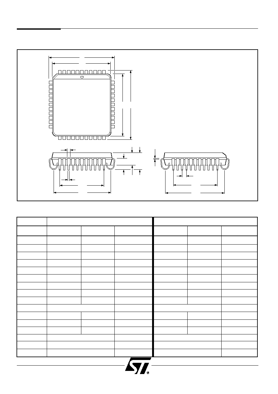
PSD3XX Family
68
Family: Plastic Leaded Chip Carrier
Millimeters
Inches
Symbol
Min
Max
Notes
Min
Max
Notes
A
4.19
4.57
0.165
0.180
A1
2.54
2.79
0.100
0.110
A2
3.76
3.96
0.148
0.156
B
0.33
0.53
0.013
0.021
B1
0.66
0.81
0.026
0.032
C
0.246
0.262
0.0097
0.0103
D
17.40
17.65
0.685
0.695
D1
16.51
16.61
0.650
0.654
D2
14.99
16.00
0.590
0.630
D3
12.70
Reference
0.500
Reference
E
17.40
17.65
0.685
0.695
E1
16.51
16.61
0.650
0.654
E2
14.99
16.00
0.590
0.630
E3
12.70
Reference
0.500
Reference
e1
1.27
Reference
0.050
Reference
N
44
44
030195R6
Drawing J2 ≠ 44-Pin Plastic Leaded Chip Carrier (PLDCC) (Package Type J)
D3
B
A1 A2
E1
E
D2
A
E2
C
D
D1
44
1
2
3
E3
e1
B1
21.0 Package Drawings
PSD3XX Family
69
Family: Ceramic Leaded Chip Carrier ≠ CERQUAD
Millimeters
Inches
Symbol
Min
Max
Notes
Min
Max
Notes
A
3.94
4.57
0.155
0.180
A1
2.29
2.92
0.090
0.115
A2
3.05
3.68
0.120
0.145
B
0.43
0.53
0.017
0.021
B1
0.66
0.81
0.026
0.032
C
0.15
0.25
0.006
0.010
D
17.40
17.65
0.685
0.695
D1
16.31
16.66
0.642
0.656
D2
14.73
16.26
0.580
0.640
D3
12.70
Reference
0.500
Reference
E
17.40
17.65
0.685
0.695
E1
16.31
16.66
0.642
0.656
E2
14.73
16.26
0.580
0.640
E3
12.70
Reference
0.500
Reference
e1
1.27
Reference
0.050
Reference
N
44
44
030195R8
Drawing L4 ≠ 44-Pin Pocketed Ceramic Leaded Chip Carrier (CLDCC) ≠ CERQUAD (Package Type L)
D3
B1
B
A1
A
E1
E
44
D2
A2
C
1
2
3
E2
D1
D
E3
e1
View A
Commercial and Industrial
packages include the lead pocket
on the underside of the package
but Military packages do not.
View A
PSD3XX Family
70
Drawing M1 ≠ 44-Pin Plastic Quad Flatpack (PQFP) (Package Type M)
B
E1
E
1
D3
E3
D1
D
L
a
2
3
44
A2
A
A1
C
Index
Mark
e1
Standoff:
0.10 mm Min
0.25 mm Max
Family: Plastic Quad Flatpack (PQFP)
Millimeters
Inches
Symbol
Min
Max
Notes
Min
Max
Notes
0∞
7∞
0∞
7∞
A
≠
2.35
≠
0.092
A1
1.075
Reference
0.042
Reference
A2
1.95
2.10
0.077
0.083
B
0.30
0.45
0.012
0.018
C
0.13
0.23
0.005
0.009
D
13.20
0.520
D1
10.00
0.394
D3
8.00
Reference
0.315
Reference
E
13.20
0.520
E1
10.00
0.394
E3
8.00
Reference
0.315
Reference
e1
0.80
Reference
0.031
Reference
L
0.73
1.03
0.029
0.040
N
44
44
030195R4
PSD3XX Family
71
Drawing U1 ≠ 44-Pin Plastic Thin Quad Flatpack (TQFP) (Package Type U)
B
E1
E
1
D3
E3
D1
D
L
a
2
3
44
A2
A
A1
C
Index
Mark
e1
Standoff:
0.05 mm Min
Lead
Coplanarity:
0.102 mm Max.
Family: Plastic Thin Quad Flatpack (TQFP)
Millimeters
Inches
Symbol
Min
Max
Notes
Min
Max
Notes
0∞
8∞
0∞
8∞
A
≠
1.60
≠
0.063
A1
0.54
0.74
0.021
0.029
A2
1.15
1.55
0.045
0.061
B
0.35
Reference
0.014
Reference
C
0.09
0.20
0.004
0.008
D
15.75
16.25
0.620
0.640
D1
13.90
14.10
0.547
0.555
D3
10.00
Reference
0.394
Reference
E
15.75
16.25
0.620
0.640
E1
13.90
14.10
0.547
0.555
E3
10.00
Reference
0.394
Reference
e1
1.00
Reference
0.039
Reference
L
0.35
0.65
0.014
0.026
N
44
44
030195R4
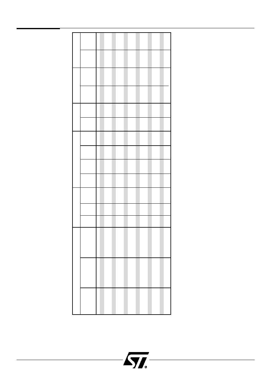
ST Part #
MCU
PLDs/Decoders
I/O
Memory
Other
PSD ZPSD
ZPSD
8-Bit 16-Bit Interface Inputs Product
PLD
Page
Ports
Open
EPROM
SRAM
Peripheral
Security
@ @
@
Data
Data
Terms
Outputs
Reg.
Drain
Mode
5 V
5 V
2.7 V
PSD311R
ZPSD311R
X
STD
14
40
11
19
X
256Kb
X
X
PSD301R
ZPSD301R
X
X
STD
14
40
11
19
X
256Kb
X
X
PSD312R
ZPSD312R
X
STD
18
40
11
X
19
X
512Kb
X
X
PSD302R
ZPSD302R
X
X
STD
18
40
11
X
19
X
512Kb
X
X
PSD313R
ZPSD313R
X
STD
18
40
11
X
19
X
1024Kb
X
X
PSD303R
ZPSD303R
X
X
STD
18
40
11
X
19
X
1024Kb
X
X
PSD311
ZPSD311
ZPSD311V
X
STD
14
40
11
19
X
256Kb
16Kb
X
X
PSD301
ZPSD301
ZPSD301V
X
X
STD
14
40
11
19
X
256Kb
16Kb
X
X
PSD312
ZPSD312
ZPSD312V
X
STD
18
40
11
X
19
X
512Kb
16Kb
X
X
PSD302
ZPSD302
ZPSD302V
X
X
STD
18
40
11
X
19
X
512Kb
16Kb
X
X
PSD313
ZPSD313
ZPSD313V
X
STD
18
40
11
X
19
X
1024Kb
16Kb
X
X
PSD303
ZPSD303
ZPSD303V
X
X
STD
18
40
11
X
19
X
1024Kb
16Kb
X
X
PSD3XX Family
72
22.1 PSD3XX Family ≠ Selector Guide
22.0
PSD3XX
Ordering
Information
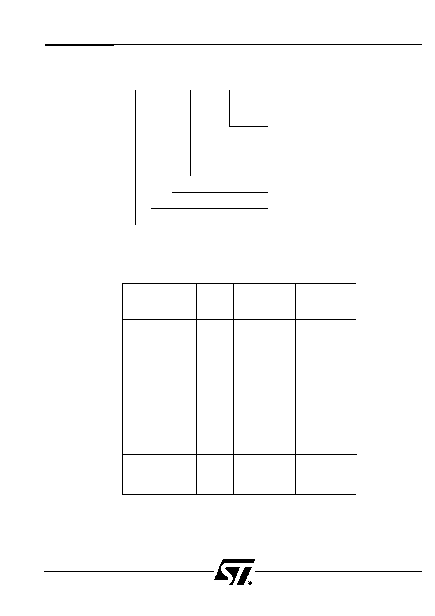
PSD3XX Family
73
PSD3XX
Ordering
Information
(cont.)
Temperature (Blank = Commercial,
I = Industrial, M = Military)
Package Type
Speed (-70 = 70ns, -90 = 90ns, -15 = 150ns
-20 = 200ns, -25 = 250ns)
Revision (Blank = No Revision)
Supply Voltage (Blank = 5V, V = 3 Volt)
Base Part Number - see Selector Guide
PSD (ST Programmable System Device) Fam.
Power Down Feature (Blank = Standard,
Z = Zero Power Feature)
Z
PSD
-A -20 J
I
413A2 V
22.2 Part Number Construction
Operating
Speed
Temperature
Part Number
(ns)
Package Type
Range
PSD301-B-70J
70
44 Pin PLDCC
Comm'l
PSD301-B-70L
70
44 Pin CLDCC
Comm'l
PSD301-B-70M
70
44 Pin PQFP
Comm'l
PSD301-B-70U
70
44 Pin TQFP
Comm'l
PSD301-B-90JI
90
44 Pin PLDCC
Industrial
PSD301-B-90LI
90
44 Pin CLDCC
Industrial
PSD301-B-90MI
90
44 Pin PQFP
Industrial
PSD301-B-90UI
90
44 Pin TQFP
Industrial
PSD301-B-15J
150
44 Pin PLDCC
Comm'l
PSD301-B-15L
150
44 Pin CLDCC
Comm'l
PSD301-B-15M
150
44 Pin PQFP
Comm'l
PSD301-B-15U
150
44 Pin TQFP
Comm'l
PSD301R-B-70J
70
44 Pin PLDCC
Comm'l
PSD301R-B-90JI
90
44 Pin PLDCC
Industrial
PSD301R-B-15J
150
44 Pin PLDCC
Comm'l
22.3 Ordering Information
PSD3XX Family
74
Operating
Speed
Temperature
Part Number
(ns)
Package Type
Range
PSD302-B-70J
70
44 Pin PLDCC
Comm'l
PSD302-B-70L
70
44 Pin CLDCC
Comm'l
PSD302-B-70M
70
44 Pin PQFP
Comm'l
PSD302-B-70U
70
44 Pin TQFP
Comm'l
PSD302-B-90JI
90
44 Pin PLDCC
Industrial
PSD302-B-90LI
90
44 Pin CLDCC
Industrial
PSD302-B-90MI
90
44 Pin PQFP
Industrial
PSD302-B-90UI
90
44 Pin TQFP
Industrial
PSD302-B-15J
150
44 Pin PLDCC
Comm'l
PSD302-B-15L
150
44 Pin CLDCC
Comm'l
PSD302-B-15M
150
44 Pin PQFP
Comm'l
PSD302-B-15U
150
44 Pin TQFP
Comm'l
PSD302R-B-70J
70
44 Pin PLDCC
Comm'l
PSD302R-B-90JI
90
44 Pin PLDCC
Industrial
PSD302R-B-15J
150
44 Pin PLDCC
Comm'l
PSD303-B-70J
70
44 Pin PLDCC
Comm'l
PSD303-B-70L
70
44 Pin CLDCC
Comm'l
PSD303-B-70M
70
44 Pin PQFP
Comm'l
PSD303-B-70U
70
44 Pin TQFP
Comm'l
PSD303-B-90JI
90
44 Pin PLDCC
Industrial
PSD303-B-90LI
90
44 Pin CLDCC
Industrial
PSD303-B-90MI
90
44 Pin PQFP
Industrial
PSD303-B-90UI
90
44 Pin TQFP
Industrial
PSD303-B-15J
150
44 Pin PLDCC
Comm'l
PSD303-B-15L
150
44 Pin CLDCC
Comm'l
PSD303-B-15M
150
44 Pin PQFP
Comm'l
PSD303-B-15U
150
44 Pin TQFP
Comm'l
PSD303R-B-70J
70
44 Pin PLDCC
Comm'l
PSD303R-B-90JI
90
44 Pin PLDCC
Industrial
PSD303R-B-15J
150
44 Pin PLDCC
Comm'l
PSD311-B-70J
70
44 Pin PLDCC
Comm'l
PSD311-B-70L
70
44 Pin CLDCC
Comm'l
PSD311-B-70M
70
44 Pin PQFP
Comm'l
PSD311-B-70U
70
44 Pin TQFP
Comm'l
PSD311-B-90JI
90
44 Pin PLDCC
Industrial
PSD311-B-90LI
90
44 Pin CLDCC
Industrial
PSD311-B-90MI
90
44 Pin PQFP
Industrial
PSD311-B-90UI
90
44 Pin TQFP
Industrial
PSD311-B-15J
150
44 Pin PLDCC
Comm'l
PSD311-B-15L
150
44 Pin CLDCC
Comm'l
PSD311-B-15M
150
44 Pin PQFP
Comm'l
PSD311-B-15U
150
44 Pin TQFP
Comm'l
PSD311R-B-70J
70
44 Pin PLDCC
Comm'l
PSD311R-B-90JI
90
44 Pin PLDCC
Industrial
PSD311R-B-15J
150
44 Pin PLDCC
Comm'l
Ordering Information
PSD3XX
Ordering
Information
(cont.)

PSD3XX Family
75
PSD3XX
Ordering
Information
(cont.)
Operating
Speed
Temperature
Part Number
(ns)
Package Type
Range
PSD312-B-70J
70
44 Pin PLDCC
Comm'l
PSD312-B-70L
70
44 Pin CLDCC
Comm'l
PSD312-B-70M
70
44 Pin PQFP
Comm'l
PSD312-B-70U
70
44 Pin TQFP
Comm'l
PSD312-B-90JI
90
44 Pin PLDCC
Industrial
PSD312-B-90LI
90
44 Pin CLDCC
Industrial
PSD312-B-90MI
90
44 Pin PQFP
Industrial
PSD312-B-90UI
90
44 Pin TQFP
Industrial
PSD312-B-15J
150
44 Pin PLDCC
Comm'l
PSD312-B-15L
150
44 Pin CLDCC
Comm'l
PSD312-B-15M
150
44 Pin PQFP
Comm'l
PSD312-B-15U
150
44 Pin TQFP
Comm'l
PSD312R-B-70J
70
44 Pin PLDCC
Comm'l
PSD312R-B-90JI
90
44 Pin PLDCC
Industrial
PSD312R-B-15J
150
44 Pin PLDCC
Comm'l
PSD313-B-70J
70
44 Pin PLDCC
Comm'l
PSD313-B-70L
70
44 Pin CLDCC
Comm'l
PSD313-B-70M
70
44 Pin PQFP
Comm'l
PSD313-B-70U
70
44 Pin TQFP
Comm'l
PSD313-B-90JI
90
44 Pin PLDCC
Industrial
PSD313-B-90LI
90
44 Pin CLDCC
Industrial
PSD313-B-90MI
90
44 Pin PQFP
Industrial
PSD313-B-90UI
90
44 Pin TQFP
Industrial
PSD313-B-15J
150
44 Pin PLDCC
Comm'l
PSD313-B-15L
150
44 Pin CLDCC
Comm'l
PSD313-B-15M
150
44 Pin PQFP
Comm'l
PSD313-B-15U
150
44 Pin TQFP
Comm'l
PSD313R-B-70J
70
44 Pin PLDCC
Comm'l
PSD313R-B-90JI
90
44 Pin PLDCC
Industrial
PSD313R-B-15J
150
44 Pin PLDCC
Comm'l
Ordering Information

PSD3XX Family
76
PSD3XX
Ordering
Information
(cont.)
Operating
Speed
Temperature
Part Number
(ns)
Package Type
Range
ZPSD301-B-70J
70
44 Pin PLDCC
Comm'l
ZPSD301-B-70L
70
44 Pin CLDCC
Comm'l
ZPSD301-B-70M
70
44 Pin PQFP
Comm'l
ZPSD301-B-70U
70
44 Pin TQFP
Comm'l
ZPSD301-B-90JI
90
44 Pin PLDCC
Industrial
ZPSD301-B-90LI
90
44 Pin CLDCC
Industrial
ZPSD301-B-90MI
90
44 Pin PQFP
Industrial
ZPSD301-B-90UI
90
44 Pin TQFP
Industrial
ZPSD301-B-15J
150
44 Pin PLDCC
Comm'l
ZPSD301-B-15L
150
44 Pin CLDCC
Comm'l
ZPSD301-B-15M
150
44 Pin PQFP
Comm'l
ZPSD301-B-15U
150
44 Pin TQFP
Comm'l
ZPSD301R-B-70J
70
44 Pin PLDCC
Comm'l
ZPSD301R-B-90JI
90
44 Pin PLDCC
Industrial
ZPSD301R-B-15J
150
44 Pin PLDCC
Comm'l
ZPSD301V-B-15J
150
44 Pin PLDCC
Comm'l
ZPSD301V-B-15L
150
44 Pin CLDCC
Comm'l
ZPSD301V-B-15U
150
44 Pin TQFP
Comm'l
ZPSD301V-B-20J
200
44 Pin PLDCC
Comm'l
ZPSD301V-B-20JI
200
44 Pin PLDCC
Industrial
ZPSD301V-B-20L
200
44 Pin CLDCC
Comm'l
ZPSD301V-B-20M
200
44 Pin PQFP
Comm'l
ZPSD301V-B-20MI
200
44 Pin PQFP
Industrial
ZPSD301V-B-20U
200
44 Pin TQFP
Comm'l
ZPSD301V-B-20UI
200
44 Pin TQFP
Industrial
ZPSD301V-B-25J
250
44 Pin PLDCC
Comm'l
ZPSD301V-B-25L
250
44 Pin CLDCC
Comm'l
ZPSD301V-B-25M
250
44 Pin PQFP
Comm'l
ZPSD301V-B-25U
250
44 Pin TQFP
Comm'l
ZPSD302-B-70J
70
44 Pin PLDCC
Comm'l
ZPSD302-B-70L
70
44 Pin CLDCC
Comm'l
ZPSD302-B-70M
70
44 Pin PQFP
Comm'l
ZPSD302-B-70U
70
44 Pin TQFP
Comm'l
ZPSD302-B-90JI
90
44 Pin PLDCC
Industrial
ZPSD302-B-90LI
90
44 Pin CLDCC
Industrial
ZPSD302-B-90MI
90
44 Pin PQFP
Industrial
ZPSD302-B-90UI
90
44 Pin TQFP
Industrial
ZPSD302-B-15J
150
44 Pin PLDCC
Comm'l
ZPSD302-B-15L
150
44 Pin CLDCC
Comm'l
ZPSD302-B-15M
150
44 Pin PQFP
Comm'l
ZPSD302-B-15U
150
44 Pin TQFP
Comm'l
ZPSD302R-B-70J
70
44 Pin PLDCC
Comm'l
ZPSD302R-B-90JI
90
44 Pin PLDCC
Industrial
ZPSD302R-B-15J
150
44 Pin PLDCC
Comm'l
Ordering Information
PSD3XX Family
77
PSD3XX
Ordering
Information
(cont.)
Operating
Speed
Temperature
Part Number
(ns)
Package Type
Range
ZPSD302V-B-20J
200
44 Pin PLDCC
Comm'l
ZPSD302V-B-20JI
200
44 Pin PLDCC
Industrial
ZPSD302V-B-20L
200
44 Pin CLDCC
Comm'l
ZPSD302V-B-20M
200
44 Pin PQFP
Comm'l
ZPSD302V-B-20MI
200
44 Pin PQFP
Industrial
ZPSD302V-B-20U
200
44 Pin TQFP
Comm'l
ZPSD302V-B-20UI
200
44 Pin TQFP
Industrial
ZPSD302V-B-25J
250
44 Pin PLDCC
Comm'l
ZPSD302V-B-25L
250
44 Pin CLDCC
Comm'l
ZPSD302V-B-25M
250
44 Pin PQFP
Comm'l
ZPSD302V-B-25U
250
44 Pin TQFP
Comm'l
ZPSD303-B-70J
70
44 Pin PLDCC
Comm'l
ZPSD303-B-70L
70
44 Pin CLDCC
Comm'l
ZPSD303-B-70M
70
44 Pin PQFP
Comm'l
ZPSD303-B-70U
70
44 Pin TQFP
Comm'l
ZPSD303-B-90JI
90
44 Pin PLDCC
Industrial
ZPSD303-B-90LI
90
44 Pin CLDCC
Industrial
ZPSD303-B-90MI
90
44 Pin PQFP
Industrial
ZPSD303-B-90UI
90
44 Pin TQFP
Industrial
ZPSD303-B-15J
150
44 Pin PLDCC
Comm'l
ZPSD303-B-15L
150
44 Pin CLDCC
Comm'l
ZPSD303-B-15M
150
44 Pin PQFP
Comm'l
ZPSD303-B-15U
150
44 Pin TQFP
Comm'l
ZPSD303R-B-70J
70
44 Pin PLDCC
Comm'l
ZPSD303R-B-90JI
90
44 Pin PLDCC
Industrial
ZPSD303R-B-15J
150
44 Pin PLDCC
Comm'l
ZPSD303V-B-20J
200
44 Pin PLDCC
Comm'l
ZPSD303V-B-20JI
200
44 Pin PLDCC
Industrial
ZPSD303V-B-20L
200
44 Pin CLDCC
Comm'l
ZPSD303V-B-20M
200
44 Pin PQFP
Comm'l
ZPSD303V-B-20MI
200
44 Pin PQFP
Industrial
ZPSD303V-B-20U
200
44 Pin TQFP
Comm'l
ZPSD303V-B-20UI
200
44 Pin TQFP
Industrial
ZPSD303V-B-25J
250
44 Pin PLDCC
Comm'l
ZPSD303V-B-25L
250
44 Pin CLDCC
Comm'l
ZPSD303V-B-25M
250
44 Pin PQFP
Comm'l
ZPSD303V-B-25U
250
44 Pin TQFP
Comm'l
Ordering Information
PSD3XX Family
78
PSD3XX
Ordering
Information
(cont.)
Operating
Speed
Temperature
Part Number
(ns)
Package Type
Range
ZPSD311-B-70J
70
44 Pin PLDCC
Comm'l
ZPSD311-B-70L
70
44 Pin CLDCC
Comm'l
ZPSD311-B-70M
70
44 Pin PQFP
Comm'l
ZPSD311-B-70U
70
44 Pin TQFP
Comm'l
ZPSD311-B-90JI
90
44 Pin PLDCC
Industrial
ZPSD311-B-90LI
90
44 Pin CLDCC
Industrial
ZPSD311-B-90MI
90
44 Pin PQFP
Industrial
ZPSD311-B-90UI
90
44 Pin TQFP
Industrial
ZPSD311-B-15J
150
44 Pin PLDCC
Comm'l
ZPSD311-B-15L
150
44 Pin CLDCC
Comm'l
ZPSD311-B-15M
150
44 Pin PQFP
Comm'l
ZPSD311-B-15U
150
44 Pin TQFP
Comm'l
ZPSD311R-B-70J
70
44 Pin PLDCC
Comm'l
ZPSD311R-B-70M
70
44 Pin PQFP
Comm'l
ZPSD311R-B-90JI
90
44 Pin PLDCC
Industrial
ZPSD311R-B-90MI
90
44 Pin PQFP
Industrial
ZPSD311R-B-15J
150
44 Pin PLDCC
Comm'l
ZPSD311R-B-15M
150
44 Pin PQFP
Comm'l
ZPSD311V-B-15J
150
44 Pin PLDCC
Comm'l
ZPSD311V-B-15L
150
44 Pin CLDCC
Comm'l
ZPSD311V-B-15M
150
44 Pin PQFP
Comm'l
ZPSD311V-B-15U
150
44 Pin TQFP
Comm'l
ZPSD311V-B-20J
200
44 Pin PLDCC
Comm'l
ZPSD311V-B-20JI
200
44 Pin PLDCC
Industrial
ZPSD311V-B-20L
200
44 Pin CLDCC
Comm'l
ZPSD311V-B-20M
200
44 Pin PQFP
Comm'l
ZPSD311V-B-20MI
200
44 Pin PQFP
Industrial
ZPSD311V-B-20U
200
44 Pin TQFP
Comm'l
ZPSD311V-B-20UI
200
44 Pin TQFP
Industrial
ZPSD311V-B-25J
250
44 Pin PLDCC
Comm'l
ZPSD311V-B-25L
250
44 Pin CLDCC
Comm'l
ZPSD311V-B-25M
250
44 Pin PQFP
Comm'l
ZPSD311V-B-25U
250
44 Pin TQFP
Comm'l
Ordering Information
PSD3XX Family
79
PSD3XX
Ordering
Information
(cont.)
Operating
Speed
Temperature
Part Number
(ns)
Package Type
Range
ZPSD312-B-70J
70
44 Pin PLDCC
Comm'l
ZPSD312-B-70L
70
44 Pin CLDCC
Comm'l
ZPSD312-B-70M
70
44 Pin PQFP
Comm'l
ZPSD312-B-70U
70
44 Pin TQFP
Comm'l
ZPSD312-B-90JI
90
44 Pin PLDCC
Industrial
ZPSD312-B-90LI
90
44 Pin CLDCC
Industrial
ZPSD312-B-90MI
90
44 Pin PQFP
Industrial
ZPSD312-B-90UI
90
44 Pin TQFP
Industrial
ZPSD312-B-15J
150
44 Pin PLDCC
Comm'l
ZPSD312-B-15L
150
44 Pin CLDCC
Comm'l
ZPSD312-B-15M
150
44 Pin PQFP
Comm'l
ZPSD312-B-15U
150
44 Pin TQFP
Comm'l
ZPSD312R-B-70J
70
44 Pin PLDCC
Comm'l
ZPSD312R-B-70M
70
44 Pin PQFP
Comm'l
ZPSD312R-B-90JI
90
44 Pin PLDCC
Industrial
ZPSD312R-B-90MI
90
44 Pin PQFP
Industrial
ZPSD312R-B-15J
150
44 Pin PLDCC
Comm'l
ZPSD312R-B-15M
150
44 Pin PQFP
Comm'l
ZPSD312V-B-20J
200
44 Pin PLDCC
Comm'l
ZPSD312V-B-20JI
200
44 Pin PLDCC
Industrial
ZPSD312V-B-20L
200
44 Pin CLDCC
Comm'l
ZPSD312V-B-20M
200
44 Pin PQFP
Comm'l
ZPSD312V-B-20MI
200
44 Pin PQFP
Industrial
ZPSD312V-B-20U
200
44 Pin TQFP
Comm'l
ZPSD312V-B-20UI
200
44 Pin TQFP
Industrial
ZPSD312V-B-25J
250
44 Pin PLDCC
Comm'l
ZPSD312V-B-25L
250
44 Pin CLDCC
Comm'l
ZPSD312V-B-25M
250
44 Pin PQFP
Comm'l
ZPSD312V-B-25U
250
44 Pin TQFP
Comm'l
ZPSD313-B-70J
70
44 Pin PLDCC
Comm'l
ZPSD313-B-70L
70
44 Pin CLDCC
Comm'l
ZPSD313-B-70M
70
44 Pin PQFP
Comm'l
ZPSD313-B-70U
70
44 Pin TQFP
Comm'l
ZPSD313-B-90JI
90
44 Pin PLDCC
Industrial
ZPSD313-B-90LI
90
44 Pin CLDCC
Industrial
ZPSD313-B-90MI
90
44 Pin PQFP
Industrial
ZPSD313-B-90UI
90
44 Pin TQFP
Industrial
ZPSD313-B-15J
150
44 Pin PLDCC
Comm'l
ZPSD313-B-15L
150
44 Pin CLDCC
Comm'l
ZPSD313-B-15M
150
44 Pin PQFP
Comm'l
ZPSD313-B-15U
150
44 Pin TQFP
Comm'l
Ordering Information
PSD3XX Family
80
PSD3XX
Ordering
Information
(cont.)
Operating
Speed
Temperature
Part Number
(ns)
Package Type
Range
ZPSD313R-B-70J
70
44 Pin PLDCC
Comm'l
ZPSD313R-B-70M
70
44 Pin PQFP
Comm'l
ZPSD313R-B-90JI
90
44 Pin PLDCC
Industrial
ZPSD313R-B-90MI
90
44 Pin PQFP
Industrial
ZPSD313R-B-15J
150
44 Pin PLDCC
Comm'l
ZPSD313R-B-15M
150
44 Pin PQFP
Comm'l
ZPSD313V-B-20J
200
44 Pin PLDCC
Comm'l
ZPSD313V-B-20JI
200
44 Pin PLDCC
Industrial
ZPSD313V-B-20L
200
44 Pin CLDCC
Comm'l
ZPSD313V-B-20M
200
44 Pin PQFP
Comm'l
ZPSD313V-B-20MI
200
44 Pin PQFP
Industrial
ZPSD313V-B-20U
200
44 Pin TQFP
Comm'l
ZPSD313V-B-20UI
200
44 Pin TQFP
Industrial
ZPSD313V-B-25J
250
44 Pin PLDCC
Comm'l
ZPSD313V-B-25L
250
44 Pin CLDCC
Comm'l
ZPSD313V-B-25M
250
44 Pin PQFP
Comm'l
ZPSD313V-B-25U
250
44 Pin TQFP
Comm'l
Ordering Information
Parts
Data Sheet
Date
Affected
Changes
May, 1995
PSD3XX
Initial Release
May, 1998
ZPSD3XX
SRAM-less (R suffix) version
added.
PQFP package added.
May, 1998
PSD3XX
PQFP package added,
Specifications updated,
PSD3XXL discontinued,
Some speed grades eliminated.
February, 1999
PSD3XXR, ZPSD3XXR
Combined Data Sheets
Updated Specifications
23.
Revisions
History
PSD3XX, ZPSD3XX, ZPSD3XXV, PSD3XXR, ZPSD3XXR, ZPSD3XXRV
2/3
REVISION HISTORY
Table 1. Document Revision History
Date
Rev.
Description of Revision
May-1995
1.0
Documents written in the WSI format. Initial release
May-1998
1.1
ZPSD3XX SRAM-less (R suffix) version added. PQFP package added.
PSD3XX PQFP package added, Specifications updated, PSD3XXL discontinued, Some speed
grades eliminated.
February, 1999 PSD3XXR, ZPSD3XXR Combined Data Sheets
Updated Specifications
Feb-1999
1.2
PSD3XX ZPSD3XX ZPSD3XXV, PSD3XXR ZPSD3XXR ZPSD3XXRV Combined Data
Sheets Updated Specifications
31-Jan-2002
1.3
PSD3XX, ZPSD3XX, ZPSD3XXV, PSD3XXR, ZPSD3XXR, ZPSD3XXRV: Low Cost Field
Programmable Microcontroller Peripherals
Front page, and back two pages, in ST format, added to the PDF file
Any references to Waferscale, WSI, EasyFLASH and PSDsoft 2000
updated to ST, ST, Flash+PSD and PSDsoft Express

3/3
PSD3XX, ZPSD3XX, ZPSD3XXV, PSD3XXR, ZPSD3XXR, ZPSD3XXRV
Information furnished is believed to be accurate and reliable. However, STMicroelectronics assumes no responsibility for the consequences
of use of such information nor for any infringement of patents or other rights of third parties which may result from its use. No license is granted
by implication or otherwise under any patent or patent rights of STMicroelectronics. Specifications mentioned in this publication are subject
to change without notice. This publication supersedes and replaces all information previously supplied. STMicroelectronics products are not
authorized for use as critical components in life support devices or systems without express written approval of STMicroelectronics.
The ST logo is registered trademark of STMicroelectronics
All other names are the property of their respective owners
© 2002 STMicroelectronics - All Rights Reserved
STMicroelectronics group of companies Australia - Brazil - Canada - China - Finland - France - Germany - Hong Kong -
India - Israel - Italy - Japan - Malaysia - Malta - Morocco - Singapore - Spain - Sweden - Switzerland - United Kingdom - United States.
www.st.com