
1/3
NOT FOR NEW DESIGN
January 2002
This is information on a product still in production but not recommended for new designs.
PSD5XX
ZPSD5XX
Low Cost Field Programmable Microcontroller Peripherals
FEATURES SUMMARY
s
Single Supply Voltage:
≠ 5 V±10% for PSD5XX
≠ 2.7 to 5.5 V for PSD5XX-V
s
Up to 1 Mbit of UV EPROM
s
Up to 16 Kbit SRAM
s
Input Latches
s
Programmable I/O ports
s
Page Logic
s
Programmable Security
Figure 1. Packages
PLDCC68 (J)
CLDCC68 (L)
TQFP68 (U)

i
PSD5XX Family
PSD5XX/ZPSD5XX
Field-Programmable Microcontroller Peripherals
Table of Contents
1
Introduction ...........................................................................................................................................................1
2
Key Features ........................................................................................................................................................3
3
Notation ................................................................................................................................................................4
4
ZPSD Background ................................................................................................................................................4
5
Integrated Power Management
TM
Operation ........................................................................................................6
6
Design Flow ..........................................................................................................................................................7
7
PSD5XX Family ....................................................................................................................................................8
8
Table 2. PSD5XX Pin Descriptions......................................................................................................................9
9
The PSD5XX Architecture ..................................................................................................................................11
9.1 The ZPLD Block..........................................................................................................................................11
9.1.1 The DPLD.........................................................................................................................................14
9.1.2 The GPLD.........................................................................................................................................14
9.1.2.1
Por A Macrocell Structure ..................................................................................................16
9.1.2.2
Port B Macrocell Structure .................................................................................................20
9.1.2.3
Port E Macrocell Structure .................................................................................................23
9.1.3 The PPLD .........................................................................................................................................26
9.1.4 The ZPLD Power Management ........................................................................................................26
9.2 Bus Interface...............................................................................................................................................29
9.2.1 Bus Interface Configuration ..............................................................................................................29
9.2.2 PSD5XX Interface to a Multiplexed Bus ...........................................................................................29
9.2.3 PSD5XX Interface to Non-Multiplexed Bus ......................................................................................30
9.2.4 Data Byte Enable..............................................................................................................................30
9.2.5 Optional Features .............................................................................................................................34
9.2.6 Bus Interface Examples....................................................................................................................34
9.3 I/O Ports......................................................................................................................................................39
9.3.1 Standard MCU I/O ............................................................................................................................39
9.3.2 PLD I/O ...........................................................................................................................................39
9.3.3 Address Out......................................................................................................................................40
9.3.4 Address In ........................................................................................................................................40
9.3.5 Data Port ..........................................................................................................................................40
9.3.6 Special Function Out ........................................................................................................................40
9.3.7 Alternate Function In ........................................................................................................................41
9.3.8 Peripheral I/O ...................................................................................................................................41
9.3.9 Open Drain Outputs..........................................................................................................................41
9.3.10 Port Registers...................................................................................................................................42
9.3.11 Port A ≠ Functionality and Structure.................................................................................................45
9.3.12 Port B ≠ Functionality and Structure.................................................................................................45
9.3.13 Port C and Port D ≠ Functionality and Structure ..............................................................................48
9.3.14 Port E ≠ Functionality and Structure.................................................................................................48
9.4 Memory Block .............................................................................................................................................52
9.4.1 EPROM ............................................................................................................................................52
9.4.2 SRAM ...............................................................................................................................................52
9.4.3 Memory Select Map..........................................................................................................................52
9.4.4 Memory Select Map for 8031 Application.........................................................................................54
9.4.5 Peripheral I/O ...................................................................................................................................56

ii
PSD5XX Family
PSD5XX/ZPSD5XX
Field-Programmable Microcontroller Peripherals
Table of Contents
(cont.)
9.5 Power Management Unit ............................................................................................................................58
9.5.1 Standby Mode ..................................................................................................................................58
9.5.2 Power Down .....................................................................................................................................58
9.5.3 Sleep Mode ......................................................................................................................................58
9.5.4 Other Power Saving Options ............................................................................................................61
9.6 PSD5XX Counter/Timer ..............................................................................................................................63
9.6.1 Counter/Timer Operation..................................................................................................................66
9.6.2 Counter/Timer Registers ..................................................................................................................81
9.7 Interrupt Controller ......................................................................................................................................95
9.7.1 Interrupt Operation ...........................................................................................................................95
9.7.2 Input/Output....................................................................................................................................100
9.7.3 PPLD Macrocell..............................................................................................................................100
9.7.4 Interrupt Flowchart..........................................................................................................................100
10.0 Page Register ...................................................................................................................................................103
11.0 Security Protection............................................................................................................................................103
12.0 System Configuration .......................................................................................................................................104
12.1
Reset Input ............................................................................................................................................108
12.2
ZPLD and Memory During Reset...........................................................................................................108
12.3
Register Values During and After Reset................................................................................................108
12.4
ZPLD Macrocell Initialization .................................................................................................................108
13.0 Specifications....................................................................................................................................................109
13.1
Absolute Maximum Ratings ...................................................................................................................109
13.2
Operating Range ...................................................................................................................................109
13.3
Recommended Operating Conditions....................................................................................................109
13.4
AC/DC Parameters ................................................................................................................................110
13.5
Example of PSD5XX Typical Power Calculation at V
CC
= 5.0 V ...........................................................111
13.6
DC Characteristics (5 V ± 10% versions) ..............................................................................................112
13.7
AC/DC Parameters ≠ ZPLD Timing Parameters ...................................................................................113
13.8
Microcontroller Interface ≠ AC/DC Parameters .....................................................................................115
13.9
DC Characteristics (ZPSD5XXV Versions) (3.0 V ± 10% versions) ......................................................120
13.10 AC/DC Parameters ≠ ZPLD Timing Parameters (3.0 V ± 10% versions)..............................................121
13.11 Microcontroller Interface ≠ AC/DC Parameters (3.0 V± 10% versions).................................................121
14.0 Timing Diagrams...............................................................................................................................................128
15.0 Pin Capacitance................................................................................................................................................134
16.0 AC Testing ........................................................................................................................................................134
17.0 Erasure and Programming................................................................................................................................134
18.0 PSD5XX Pin Assignments ................................................................................................................................135
19.0 Package Information .........................................................................................................................................137
20.0 PSD5XX Product Ordering Information ............................................................................................................142
20.1
PSD5XX Family ≠ Selector Guide .........................................................................................................142
20.2
Part Number Construction .....................................................................................................................143
20.3
Ordering Information..............................................................................................................................143
21.0 Process Change Notice, October 1, 1998 ........................................................................................................148
1
1.0
Introduction
Programmable Peripheral
PSD5XX Family
Field-Programmable Microcontroller Peripherals
The PSD5XX family is a microcontroller peripheral that integrates high-performance and
user-configurable blocks of EPROM, programmable logic, and SRAM into one part. The
PSD5XX is also loaded with a variety of features, such as Counter/Timers, Interrupt
controller, power management, and page logic. The PSD5XX products also provide a
powerful microcontroller interface that eliminates the need for external "glue logic". The no
"glue logic" concept provides a user-programmable interface to a variety of 8- and 16-bit
(multiplexed or non-multiplexed) microcontrollers that is easy to use. The part's integration,
small form factor, low power consumption, and ease of use make it the ideal part for
interfacing to virtually any microcontroller.
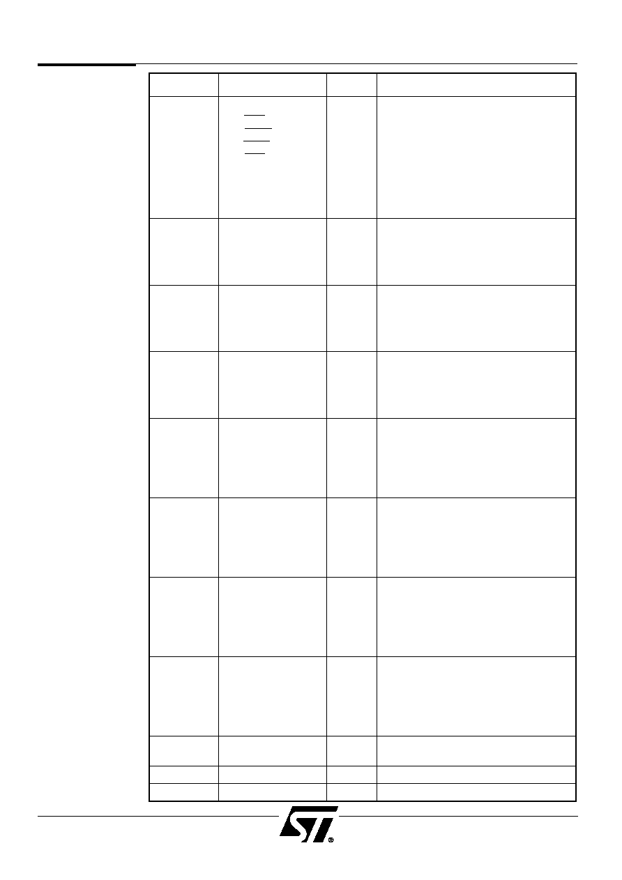
The PSD5XX provides three Zero-power PLDs (ZPLDs): a Decode PLD (DPLD), a
General-purpose PLD (PLD), and a Peripheral PLD (PPLD). The ZPLDs have a total of 61
inputs, 140 product terms, 30 macrocells, and 24 I/O connections. A configuration bit
(Turbo) can be set by the MCU, and will automatically place the ZPLDs into standby if
no inputs are changing. The ZPLDs are designed to consume minimum power using Zero
Power CMOS technology that uses low standby current. Unused product terms are
automatically disabled, also reducing power, regardless of the Turbo bit setting.
The main function of the DPLD is to perform address decoding for the internal I/O ports,
EPROM, and SRAM. The address decoding can be based on up to 24 bits of address
inputs, control signals (RD, WR, PSEN, etc.), and internal page logic. The DPLD supports
separate program and data spaces (for 8031 compatible MCUs).
The General-purpose PLD (GPLD) can be used to implement various logic defined by the
user, such as:
∑
State machines
∑
Loadable counters and shift registers
∑
Inter-processor mailbox
∑
External control logic (chip selects, output enables, etc.).
The GPLD has access to up to 61 inputs, 118 product terms, 24 macrocells, and 24 I/O
pins.

PSD5XX Family
2
Please refer to the revision block at
the end of this document for updated
information.
The Peripheral PLD (PPLD) generates outputs to the Counter/Timer unit and the Interrupt
Controller. The PPLD outputs to the Counter/Timer enable, disable, or trigger counting or
time capture. The PPLD outputs to the Interrupt Controller enables the user to define
conditions for interrupt generation.
The Counter/Timer unit provides four 16-bit highly flexible Counter/Timers. Each has five
modes of operation: pulse, waveform, event counting, time capture, and watchdog
(real-time clock). Each Counter/Timer can be programmed to count up or down. The inputs
to the Counter/Timer, which enable/disable counting or trigger an operation, can originate
from the PPLD directly or directly from the pins. The maximum operating frequency of each
counter is 7.5 MHz. The input clock can be divided (by up to 280) before driving the
Counter/Timer unit using the 4 to 280 prescaler.
The Interrupt Controller has eight levels of priority encoding. It accepts four user-defined
interrupts and four terminal counts from the Counter/Timer. Each interrupt can be
individually masked and configured to be level or edge sensitive. A 3-bit interrupt vector is
generated that can be read by the microcontroller. The serviced interrupt will be cleared
automatically after the microcontroller has read the interrupt vector.
The PSD5XX has 40 I/O pins that are divided among 5 ports. Each I/O pin can be
individually configured to provide many functions, including the following:
∑
MCU I/O
∑
ZPLD I/O
∑
Latched address output (for MCUs with multiplexed data bus)
∑
Special function I/O (Counter/Timer and Interrupts)
∑
Data bus (for MCUs with non-multiplexed data bus).
The PSD5XX can easily interface with virtually any 8- or 16-bit microcontroller with a
multiplexed or non-multiplexed bus. All of the MCU control signals are connected to the
ZPLDs, enabling the user to generate signals for external devices. The PSD5XX can
generate a reset output based on the RESET input (includes hysteresis).
The PSD5XX provides between 256 Kbits and 1 Mbit of EPROM that is divided in to four
equal-sized blocks. Each block can occupy a different address location, allowing for
versatile address mapping. The access time of the EPROM includes the address latching
and DPLD decoding.
The PSD5XX has an optional 16 Kbit SRAM that can be battery-backed by connecting a
battery to the Vstby pin. The battery will protect the contents of the SRAM in the event of a
power failure. Therefore, you can place data in the optional SRAM that you want to keep
after the power is switched off. Power switch-over to the battery automatically occurs when
Vcc drops below Vstby.
A four-bit Page Register enables easy access to the I/O section, EPROM, and SRAM for
microcontrollers with limited address space. The Page Register outputs are connected to
the ZPLDs and thus can also be used for external paging schemes.
Introduction
(cont.)

PSD5XX Family
3
2.0
Key Features
Introduction
(cont.)
The Power Management Unit (PMU) of the PSD5XX enables the user to control the
power consumption on selected functional blocks, based on system requirements. For
microcontrollers that do not generate a chip select input for the PSD, the Automatic
Power-Down (APD) unit of the PMU can be setup to enable the PSD to enter Power Down
or Sleep Mode, based on the inactivity of ALE (or AS).
Implementing your design has never been easier than with PSDsoft--WSI's software
development suite. Using PSDsoft, you can do the following:
∑
Configure your PSD5XX to work with virtually any microcontroller
∑
Specify what you want implemented in the programmable logic using a design file
∑
Simulate your design
∑
Download your design to the part using a programmer.
t
Single-chip programmable peripheral for microcontroller-based applications
t
256K to 1 Mbit of UV EPROM with the following features:
∑
Configurable as 32, 64, or 128 K x 8; or as 16, 32, or 64 K x 16
∑
Divided into four equally-sized mappable blocks for optimized address mapping
∑
As fast as 70 ns access time, which includes address decoding
∑
Built-in Zero-power technology
t
16 Kbits SRAM is configurable as 2K x 8 or 1K x 16. The access time can be
as quick as 70 ns, including address decoding. The contents of the SRAM can be
battery-backed by connecting a battery to the Vstby pin. The SRAM was also designed
using Zero-power technology
t
40 I/O pins (divided into five 8-bit ports) that can be individually configured for:
∑
Standard MCU I/O
∑
PLD/macrocell I/O
∑
Latched address output
∑
High-order address inputs
∑
Special function I/O
∑
Open-drain output
t
Three Zero-power Programmable Logic Devices (ZPLDs): the Decode PLD (DPLD), the
General-purpose PLD (GPLD), and the Peripheral PLD (PPLD) can be used for:
∑
Up to 61 input and 140 output product terms
∑
24 Macrocells and I/O
∑
Decode up to 16 MB of address
∑
State machines and state logic
∑
Generate external signals (chip selects, bus interface, etc.)
t
Microcontroller logic that eliminates the need for external "glue logic" has the following
features:
∑
Ability to interface to multiplexed and non-multiplexed buses
∑
Built-in address latches for multiplexed address/data bus
∑
ALE and Reset polarity are programmable
∑
Multiple configurations are possible for interface to many different microcontrollers
t
Four 16-bit Counter/Timers that have five modes of operation and can be controlled by
the PPLD macrocells. Modes of operation are: pulse and waveform generation, time
capture, event counting, and a watchdog timer (real time clock).
t
Eight input priority encoded Interrupt Controller. Four interrupts are generated by
the PPLD and are user defined. The other four interrupts are generated by the
Counter/Timer's terminal count flags. Each interrupt can be individually masked and
configured as edge or level sensitive.
t
Page logic is connected to the ZPLDs and expands the MCU address space to up to
16 times

PSD5XX Family
4
Key Features
(cont.)
t
Programmable power management allows:
∑
SRAM, EPROM, and ZPLDs to enter standby mode automatically
∑
Disabling of the clock input to the ZPLDs
∑
ZPLDs to enter a special low power mode (Sleep Mode), based on Turbo bit setting
t
A security bit prevents reading the PSD5XX configuration and the ZPLD contents.
Setting this bit will prevent the device from being copied on a device programmer.
t
Built-in security enables the user to block read accesses from a device programmer
t
Package choices include a 68-pin PLCC and CLDCC, and an 80-pin TQFP.
t
Programmable polarity Reset output (includes hysteresis), based on Reset input
t
Simple, menu-driven software (PSDsoft) allows configuration and design entry on a PC.
3.0
Notation
Throughout this data sheet, references are made to the PSD5XX. In most cases, these
references also cover the ZPSD5XX and ZPSD5XXV products. Exceptions will be noted.
The main difference between the ZPSD5XX and the PSD5XX is the standby current (Isb).
The ZPSD5XX devices have been rated for a lower standby current. Also, there is no
low-voltage version of the PSD5XX. There is only the low-voltage version of the ZPSD5XX,
which has a V suffix.
4.0
ZPSD
Background
Portable and battery powered systems have recently become major embedded control
application segments. As a result, the demand for electronic components having extremely
low power consumption has increased dramatically. Recognizing this need, WSI, Inc.
has developed a new Zero-Power technology. ZPSD products virtually eliminate the DC
component of power consumption reducing it to standby levels. Eliminating the DC
component is the basis for the words "Zero Power". ZPSD products also minimize the
AC power component when the chip is changing states. The result is a programmable
microcontroller peripheral family that replaces discrete circuit functions while drawing
minimal power.
PSD5XX Family
5
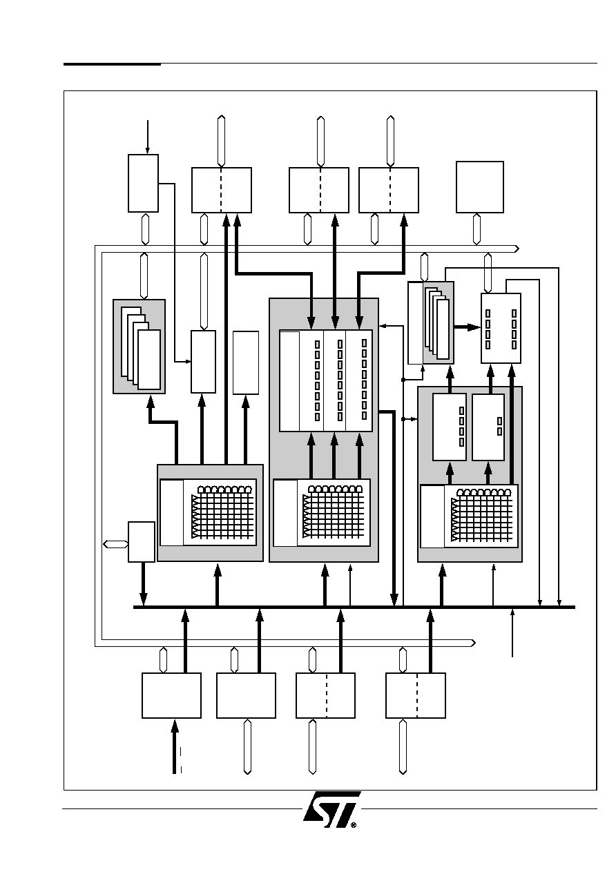
PROG.
BUS
INTRF
ADIO
PORT
CONTROL
RD, WR
AD0 ≠ AD15
PC0 ≠ PC7
PD0 ≠ PD7
CLKIN
WATCH DOG OUTPUT
INTERRUPT OUTPUT
CLKIN
60
CLKIN
TERMINAL
COUNTS
PAGE
REG.
ZPLD
INPUT
BUS
GLOBAL
CONFIG.
&
SECURITY
PROG.
PORT
PORT
A
PROG.
PORT
PORT
B
POWER
MANAGER
UNIT
VSTDBY
PA0 ≠ PA7
PB0 ≠ PB7
PROG.
PORT
PORT
E
PROG.
PORT
PORT
D
PROG.
PORT
PORT
C
PE0 ≠ PE7
ADDRESS
/
DATA
/
CONTROL BUS
4
MACROCELLS
2
MACROCELLS
8PT
4PT
2PT
PORT A MACROCELLS
PORT B MACROCELLS
PORT E MACROCELLS
27PT
61
60
80PT
11PT
CLKIN
FOUR 16
-
BIT
256K
≠
1M BIT
EPROM
16 K BITS
SRAM
I/O
DECODER
EPROM
SELECT
SRAM
SELECT
PERIPHERAL
SELECTS
MACROCELL FEEDBACK OR PORT INPUT
CSIOP
GENERAL PLD
(GPLD)
PERIPHERAL
PLD (PPLD)
INTERRUPT
CONTROLLER
COUNTER/
TIMERS
24 MACROCELLS
DECODE PLD
(DPLD)
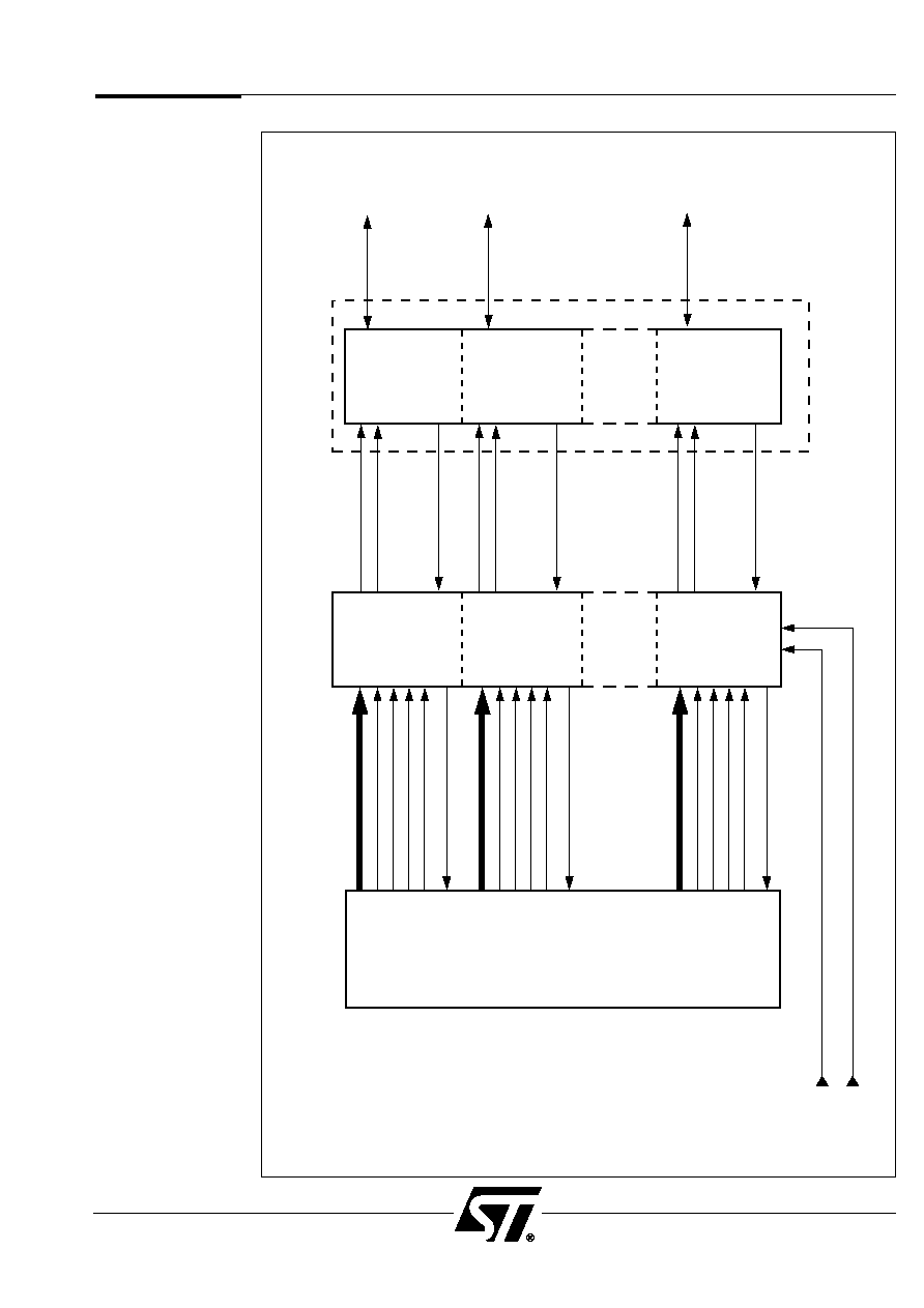
Figure 1. PSD5XX Block Diagram

PSD5XX Family
6
Upon each address or logic input change to the PSD, the device powers up from low power
standby for a short time. Then the PSD consumes only the necessary power to deliver new
logic or memory data to its outputs as a response to the input change. After the new
outputs are stable, the PSD latches them and automatically reverts back to standby mode.
The I
CC
current flowing during standby mode and during DC operation is identical.
The PSD automatically reduces its DC current drain to these low levels and does not
require controlling by the CSI (Chip Select) input. Disabling the CSI pin unconditionally
forces the PSD to standby mode independent of other input transitions.
The only significant power consumption in the PSD occurs during AC operation.
The PSD contains the first architecture to apply Zero-power techniques to memory circuit
blocks as well as logic.
Figure 2 compares PSD Zero-power operation to the operation of a discrete solution.
A standard microcontroller (MCU) bus cycle usually starts with an ALE (or AS) pulse and
the generation of an address. The PSD detects the address transition and powers up for a
short time. The PSD then latches the outputs of the PAD, EPROM and SRAM to the new
values. After finishing these operations, the PSD shuts off its internal power, entering
standby mode. The time taken for the entire cycle is less than the PSD's "access time."
The PSD will stay in standby mode if the inputs do not change between bus cycles. In an
alternate system implementation using discrete EPROM, SRAM and other discrete
components, the system will consume operating power during the entire bus cycle. This is
because the chip select inputs on the memory devices are usually active throughout the
entire cycle. The AC power consumption of the PSD may be calculated using the composite
frequency of the MCU address and control inputs, as well as any other logic inputs to the
ZPLD.
NOTE: The ZPSD5XX parts have been rated for a lower standby current (I
SB
) than the
PSD5XX parts.
5.0
Integrated
Power
Management
TM
Operation
ALE
DISCRETE EPROM, SRAM & LOGIC
ADDRESS
EPROM
ACCESS
SRAM
ACCESS
EPROM
ACCESS
I
CC
ZPSD
ZPSD
ZPSD
TIME
Figure 2. ZPSD Power Operation vs. Discrete Implementation
PSD5XX Family
7
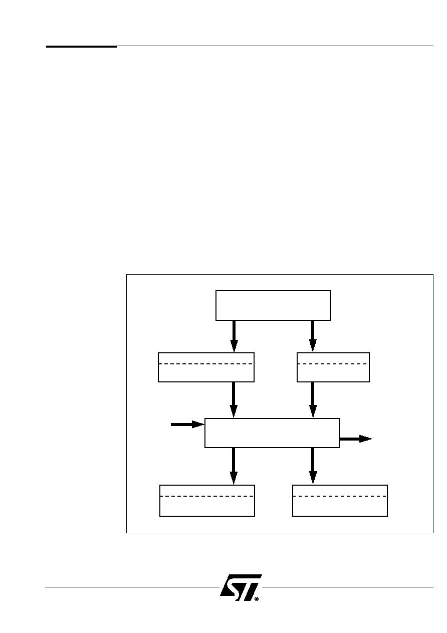
Figure 3. PSDsoft Development Tools
PSDsilos IIITM
SILOSIII
CHIP SIMULATION
PSD Programmer
PSDpro/MagicPro
Æ
CHIP PROGRAMMING
PSD Compiler
(ZPLD FITTING, ADDRESS TRANSLATION)
PSDabelTM
ZPLD DESCRIPTION
(STATE MACHINE, DECODING)
PSDsoft
Development Software
PSD Configuration
CHIP CONFIGURATION
THIRD PARTY
PROGRAMMERS
CODE FILE
Shown in Figure 3 (below) is the software design flow for a PSD5XX device.
PSDsoft--WSI's software development suite--is used throughout the design phase. You
start with a design file that is written in PSDabel-a high-level hardware description language
(HDL). Before you compile your design, you must also configure the PSD5XX so it knows
what signals to expect from your microprocessor and what pre-runtime options should be
set (such as the security bit).
Once you have a design file and have configured the device, you are ready to run the Fitter
and Address Translator. The Fitter accepts input from PSDabel and PSD Configuration,
synthesizes this user logic and configuration, and fits the design to the PSD silicon.
The Address Translator process allows the user to map the MCU firmware from a
cross-compiler (in Intel HEX or S-Record format) into the NVM memory blocks within the
PSD. As a result, the MCU firmware is merged with the logic and configuration definition of
the PSD.
The output of the Address Translator and the Fitter is the required object file that is used by
a programmer to program the PSD device. The object file includes chip configuration, the
PLD fusemap, and MCU firmware information.
PSDsilosIII is an optional program that provides functional chip-level simulation of the
PSD5XX. PSDsoft automatically creates files for input to the simulator. These files convey
relevant design information to the simulator. As a result, the user only has to create a stim-
ulus file since all of the signals and node names are taken from the design file.
6.0
Design Flow

PSD5XX Family
8
7.0
PSD5XX
Family
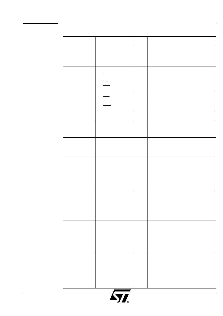
There are 7 unique devices in the PSD5XX family. The part classifications are based on
EPROM size and data bus width. The features of each part are listed in Table 1.
Part
Bus
DPLD + GPLD + PPLD
I/O Timers
Inter.
WD
*
PMU EPROM SRAM
#
Bit
Inputs Product Registered Pins
Contr.
K bit
K bit
Terms
Macrocells
501B1 x8/x16
61
140
30
40
4
*
16
8
1
*
16
Yes
256
16
511B1
x8
61
140
30
40
4
*
16
8
1
*
16
Yes
256
16
502B1 x8/x16
61
140
30
40
4
*
16
8
1
*
16
Yes
512
16
512B0
x8
61
140
30
40
4
*
16
8
1
*
16
Yes
512
≠
512B1
x8
61
140
30
40
4
*
16
8
1
*
16
Yes
512
16
503B1 x8/x16
61
140
30
40
4
*
16
8
1
*
16
Yes
1024
16
513B1
x8
61
140
30
40
4
*
16
8
1
*
16
Yes
1024
16
Table 1. PSD5XX Product Matrix
WD
= WatchDog Timer.
PMU = Power Management Unit.
*
One of the four 16-Bit Timers.
PSD5XX Family
9
8.0
Table 2.
PSD5XX Pin
Descriptions
Pin Name
Pin Function
Type
Function Descriptions
ADIO0 ≠ ADIO15
Address/ data bus
I/O
1. Address/data bus, multiplexed
bus mode
2. Address bus, non-multiplexed
bus mode
RD
Multiple Names
I
Multiple functions
1. Read
1. Read signal
2. E
2. E signal (Clock)
3. DS
3. Data strobe signal
4. LDS
4. Low byte data strobe
WR
Multiple Names
I
Multiple functions
1. WR
1. Write signal
2. R/W
2. Read-write signal
3. WRL
3. Low byte write signal
CSI
Chip Select Input
I
Active low, select PSD5XX.
standby mode if high.
RESET
Reset Input
I
Reset I/O ports, ZPLD/macrocells,
Timers and Configuration
Registers. Active low.
CLKIN
Input clock
I
Clock input to Timers, ZPLD
macrocells, ZPLD array, and APD
counter; connect to ground if clock
input not used.
PA0 ≠ PA7
I/O Port A
I/O
Multiple functions
1. I/O port
2. ZPLD/macrocell I/O port
3. Latched address outputs
(PA0≠PA7)
(A0≠A7)
4. High address inputs (A16 ≠ A23)
5. Timer outputs (PA0 ≠ PA3)
PB0 ≠ PB7
I/O Port B
I/O
Multiple functions
1. I/O port
2. ZPLD/macrocell I/O port
3. Latched address outputs
(PB0≠PB7)
(A0≠A7) or (A8≠A15)
4. Timer outputs (PB0-PB3)
PC0 ≠ PC7
I/O Port C
I/O
Multiple functions
CMOS
1. I/O port
or
2. ZPLD input port
OD
3. Latched address outputs
(PC0 ≠ PC7)
(A0≠A7)
4. Data Port (D0 ≠ D7,
non-multiplexed bus)
PD0 ≠ PD7
I/O Port D
I/O
Multiple functions
CMOS
1. I/O port
or
2. ZPLD input port
OD
3. Latched address outputs
(PD0≠PD7)
(A0≠A7) or (A8≠A15)
4. Data Port (D8-D15,
non-multiplexed bus)
The following table describes the pin names and pin functions of the PSD5XX. Pins that
have multiple names and/or functions are defined by user configuration.
Pin Name
Pin Function
Type
Function Descriptions
PE0
Port PE, pin 0
I/O
Multiple functions
1. BHE
1. High byte enable, 16 bit data
2. PSEN
2. Read program memory, 8031 signal
3. WRH
write high data byte
4. UDS
4. Upper Data Strobe
5. SIZ0
5. Byte enable, 68300 signal
6. PE0
6. I/O pin
7. PE0
7. ZPLD I/O pin
8. PE0
8. Latched Address Out ≠ A0
PE1
Port PE, pin 1
I/O
Multiple functions
1. ALE
1. Address strobe
2. PE1
2. I/O pin
3. PE1
3. ZPLD I/O pin
4. PE1
4. Latched Address Out ≠ A1
PE2
Port PE, pin 2
Multiple functions
1. Intr Out
1. Interrupt Controller Output
2. PE2
I/O
2. I/O pin
3. PE2
3. ZPLD I/O pin
4. PE2
4. Latched Address Out ≠ A2
PE3
Port PE, pin 3
Multiple functions
1. Timer0-In
1. Timer0 control input
2. PE3
I/O
2. I/O pin
3. PE3
3. ZPLD I/O pin
4. PE3
4. Latched Address Out ≠ A3
PE4
Port PE, pin 4
Multiple functions
1. Timer1-In
1. Timer1 control input
2. PE4
I/O
2. I/O pin
3. PE4
3. ZPLD I/O pin
4. PE4
4. Latched Address Out ≠ A4
5. TC0
5. Timer0 Terminal Count
PE5
Port PE, pin 5
Multiple functions
1. Timer2-In
1. Timer2 control input
2. PE5
I/O
2. I/O pin
3. PE5
3. ZPLD I/O pin
4. PE5
4. Latched Address Out ≠ A5
5. TC1
5. Timer1 Terminal Count
PE6
Port PE, pin 6
Multiple functions
1. Timer3-In
1. Timer3 control input
2. PE6
I/O
2. I/O pin
3. PE6
3. ZPLD I/O pin
4. PE6
4. Latched Address Out ≠ A6
5. TC2
5. Timer2 Terminal Count
PE7
Port PE, pin 7
Multiple functions
1. APD CLK
1. Automatic Power Down Clock Input
2. PE7
I/O
2. I/O pin
3. PE7
3. ZPLD I/O pin
4. PE7
4. Latched Address Out ≠ A7
5. TC3
5. Timer3 Terminal Count
VSTBY
VSTBY
I
SRAM power pin for standby
operation (battery backup)
V
CC
V
CC
I
Chip V
CC
power pin
GND
GND
I
Chip ground pin
PSD5XX Family
10
Table 2.
PSD5XX Pin
Descriptions
(Cont.)

PSD5XX Family
11
9.0
The PSD5XX
Architecture
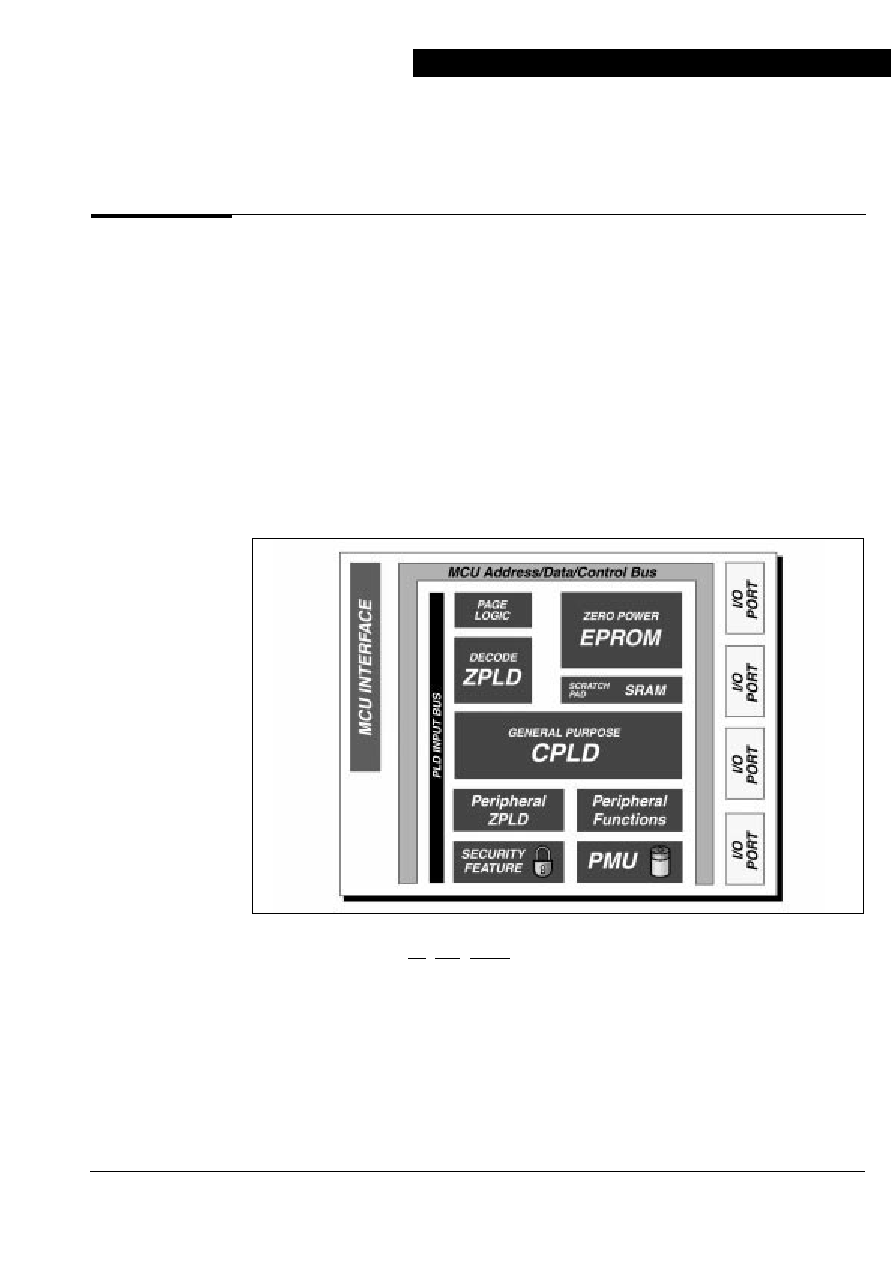
PSD5XX consists of seven major functional blocks:
t
ZPLD Blocks
t
Bus Interface
t
I/O Ports
t
Memory Block
t
Power Management Unit
t
Counter/Timer
t
Interrupt Controller
The functions of each block are described in the following sections. Many of the blocks
perform multiple functions, and are user configurable. The chip configurations are specified
by the user in the PSDsoft Development Software; some are specified by setting up the
appropriate bits in the configuration registers during run time.
9.1 ZPLD Block
Key Features
t
3 Embedded ZPLD devices
t
Maximum 30 macrocells
t
Combinatorial/registered outputs
t
Maximum 140 product terms
t
Programmable output polarity
t
User configured register clear/preset
t
User configured register clock input
t
61 Inputs
t
Accessible via 24 I/O pins
t
Power Saving Mode
t
UV-Erasable
t
Generate user defined interrupts to Interrupt Controller
and controls to Counter/ Timer
General Description
The ZPLD block has 3 embedded PLD devices:
t
DPLD
The Address Decoding PLD, generating select signals to internal I/O or memory blocks.
t
GPLD
The General Purpose PLD provides 24 programmable macrocells for general or
complex logic implementation; dedicated to user application.
t
PPLD
The Peripheral PLD, includes 6 programmable macrocells. The PPLD provides control
to the operation of the Counter/Timer and Interrupt Controller.
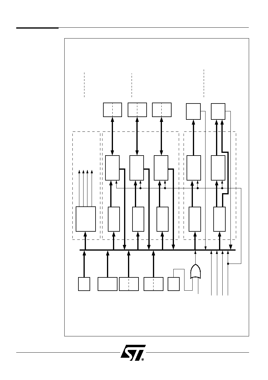
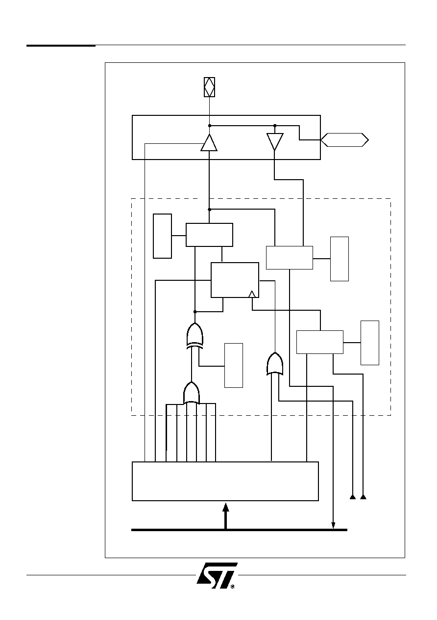
Figure 4 shows the architecture of the ZPLD. The PLD devices all share the same
input bus. The true or complement of the 61 input signals are fed to the programmable
AND-ARRAY. Names and source of the input signals are shown in Table 3. The PA, PB, PE
signals, depending on user configuration, can either be macrocell feedbacks or inputs from
Port A, B or E.
PSD5XX Family
12
Figure 4. ZPLD Block Diagram
PAGE
REG.
ADIO
PORT
PROG.
PORT
PORT
C
PROG.
PORT
PORT
D
PMU
CSI
RD/
E/DS
WR
/
R_W
RESET
CLKIN
PGR0 ≠ 3
A8 ≠ A15
A0, A1
PC0 ≠ PC7
PD0 ≠ PD7
INTR2PLD
AND
ARRAY
AND
ARRAY
AND
ARRAY
AND
ARRAY
AND
ARRAY
DPLD
ES0 ≠ ES3
RS0
CSIOP
PSEL0 ≠ PSEL1
8 I
/
O
MACROCELLS
PA
8 I
/
O
MACROCELLS
PB
8 I
/
O
MACROCELLS
PE
4 OUTPUT
4 OUTPUT
MACROCELLS
2 OUTPUT
MACROCELLS
27 PT
80 PT
11 PT
8 PT
4 PT
2 PT
PT2INT4 ≠ 5
MC2INT6 ≠ 7
MC2TMR0 ≠ 3
PE0 ≠ PE7
PB0 ≠ PB7
PA0 ≠ PA7
PROG.
PORT
PORT
A
PROG.
PORT
PORT
B
PROG.
PORT
PORT
E
TIMERS
INTR.
CTRL
DPLD
GPLD
PPLD
ZPLD INPUT
BUS
(DECODING PLD)
(GENERAL
PURPOSE PLD)
(PERIPHERAL PLD)
WDOG2PLD
The PSD5XX
Architecture

PSD5XX Family
13
Signal Name
From
PA0 ≠ PA7
Port A inputs or Macrocell PA feedback
PB0 ≠ PB7
Port B inputs or Macrocell PB feedback
PE0 ≠ PE7
Port E inputs or Macrocell PE feedback
PC0 ≠ PC7
Port C inputs
PD0 - PD7
Port D inputs
PGR0 ≠ PGR3
Page Mode Register
WDOG2PLD
Counter/Timer
INTR2PLD
Interrupt Controller
A8 ≠ A15, A0, A1
MCU Address Lines
RD/E/DS
MCU bus signal
WR/R_W
MCU bus signal
CLKIN
Input Clock
RESET
Reset input
CSI
CSI input (ORed with power down from PMU)
Table 3. ZPLD Input Signals
The PSD5XX
Architecture
(cont.)

PSD5XX Family
14
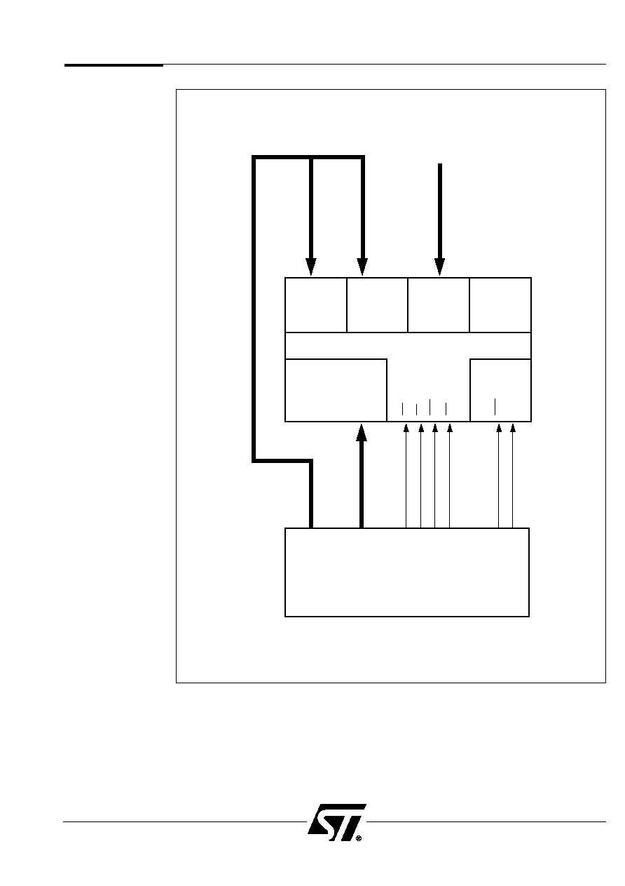
9.1.1 The DPLD
The DPLD is used for internal address decoding generating the following eight
chip select signals:
t
ES0 ≠ ES3
EPROM selects, block 0 to block 3
t
RS0
SRAM block select
t
CSIOP
I/O Decoder chip select
t
PSEL0 ≠ PSEL1
Peripheral I/O mode select signals
The I/O Decoder enabled by the CSIOP generates chip selects for on-chip registers or I/O
ports based on address inputs A[7:0].
As shown in Figure 5, the DPLD consists of a large programmable AND ARRAY. There are
a total of 61 inputs and 8 outputs. Each output consists of a single product term. Although
the user can generate select signals from any of the inputs, the select signals are typically a
function of the address and Page Register inputs. The select signals, which are active High,
are defined by the user in the ABEL file (PSDabel).
The address line inputs to the DPLD include A0, A1 and A8 ≠ A15. If more address lines
are needed, the user can bring in the lines through Port A to the DPLD.
9.1.2 The GPLD
The structure of the General Purpose PLD consists of a programmable AND ARRAY and
3 sets of I/O Macrocells. The ARRAY has 61 input signals, same as the DPLD. From these
inputs, "ANDed" functions are generated as product term inputs to the macrocells. The I/O
Macrocell sets are named after the I/O Ports they are linked to, e.g., the macrocells
connected to Port A are named PA Macrocells. The 3 sets of macrocells, PA, PB and PE,
are similar in structure and function.
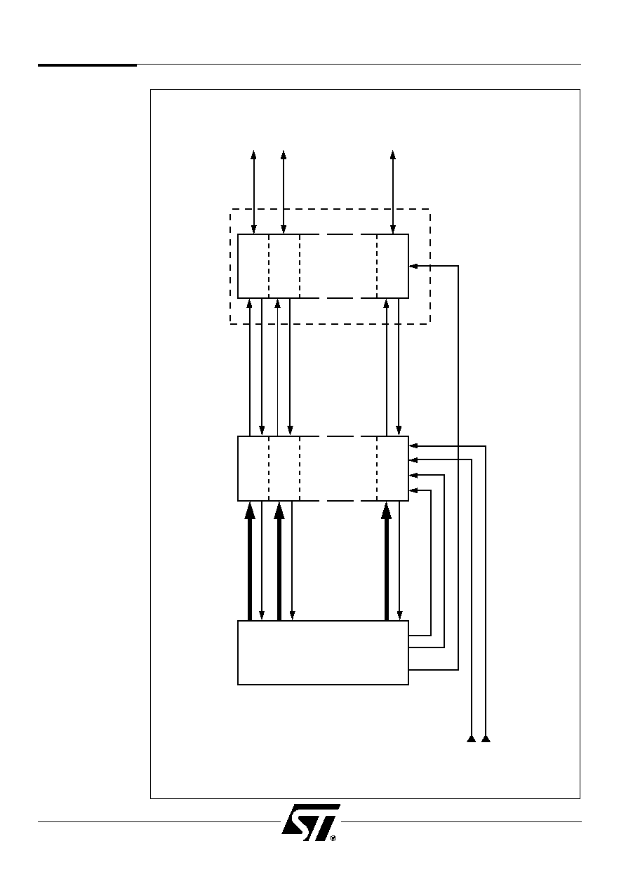
Figure 6 shows the output/input path of a GPLD macrocell to the Port pin with which it is
associated. If the Port pin is specified as a GPLD output pin in PSDsoft, the MUX in the I/O
Port Cell selects the GPLD macrocell as an output of the Port pin. The output enable signal
to the buffer in the I/O cell can be controlled by a product term from the AND ARRAY.
If the Port pin is specified as a ZPLD input pin, the MUX in the GPLD macrocell selects the
Port input signal to be one of the 61 signals in the ZPLD Input Bus.
The PSD5XX
Architecture

PSD5XX Family
15
Figure 5. DPLD Logic Array
PA0 ≠ PA7
(8)
(8)
(8)
(8)
(8)
(4)
(10)
(2)
(3)
(1)
(1)
(INPUTS)
PB0 ≠ PB7
PE0 ≠ PE7
PC0 ≠ PC7
PD0 ≠ PD7
PGR0 ≠ PGR3
A8 ≠ A15, A0, A1
WDOG2PLD
INTR2PLD
CSI, CLKIN
RESET
R
D
/E/D
S
WR
/R_W
ES0
ES1
ES2
ES3
RS0
CSIOP
PSEL0
PSEL1
4 EPROM
BLOCK
SELECTS
RAM SELECT
I
/O DECODER
SELECT
PERIPHERAL
I
/O SELECTS
DPLD INPUTS : 61
DPLD OUTPUTS : 8
The PSD5XX
Architecture
(cont.)

PSD5XX Family
16
The PSD5XX
Architecture
(cont.)
9.1.2.1 Port A Macrocell Structure
Figure 6a shows the PA Macrocell block, which consists of 8 identical macrocells.
Each macrocell output can be connected to its own I/O pin on Port A. There are 3 user
programmable global product terms output from the GPLD's AND ARRAY which are
shared by all the macrocells in Port A:
t
PA.OE
Enable or tri-state Port A output pins
t
PA.PR
Preset D flip flop in the macrocells
t
PA.RE
Reset/Clear D flip flop in the macrocells
Two other inputs, CLKIN and MACRO-RST, are used as clock and clear inputs to the D flip
flop. The CLKIN comes directly from the CLKIN input pin. The MACRO-RST is the same as
the Reset input pin except it is user configurable.
The circuit of a Port A Macrocell is shown in Figure 7. There are 6 product terms from the
GPLD's AND ARRAY as inputs to the macrocell. Users can select the polarity of the output,
and configure the macrocell to operate as:
t
Registered Output
Select output from D flip flop
t
Combinatorial Output
Select output from OR gate
t
GPLD Input
Use Port A pin as dedicated input
t
GPLD Output
Use Port A pin as dedicated output
t
GPLD I/O
Use Port A pin as bidirectional pin
t
Macrocell Feedback
Register feedback for state machine implementations or expander feedback
from the combinatorial output, to expand the number of product terms available to
another macrocell.
In case of "Buried Feedback", where the output of the macrocell is not connected to a
Port A pin, Port A can be configured to perform other user defined I/O functions.
The two global product terms assigned for asynchronous clear (PA.RE) and preset (PA.PR)
are mainly for proper Port A Macrocell initialization. The macrocell flip-flop can also be
cleared during reset by MACRO-RST, if such an option is chosen. The clock source is
always the input clock CLKIN.

PSD5XX Family
17
DQ
FIGURE 5
AND
ARRAY
POLARITY
SELECT
CL
CK
PR
CONTROL
CLK
SELECT
MUX
PT CLOCK
PT OUTPUT ENABLE (OE)
PT RESET
GPLD MACROCELL
I/O PORT CELL
PT CLEAR
CLKIN
MACRO_RST
GLOBAL
CLOCK
PORT
PIN
COMB./REG.
SELECT
GPLD
MACROCELL
OUTPUT
INTERNAL
ADDRESS
/
DATA/CONTROL
BUS
ZPLD
INPUT
BUS
MUX
MUX
MUX
PCR
D
D
Q
Q
WR
DIRECTION
REGISTER
DQ
WR
D
G
Q
ALE
PDR
PORT INPUT
INPUT
OUTPUT
ADDRESS
A[0-7]
OR
A[8-15]
GPLD
OUTPUT
SPECIAL
FUNCTION
PTs
LATCH
ALE
60
*
*
= LATCH ONLY
ON PORT A
Figure 6. GPLD Macrocell Input/Output Port
The PSD5XX
Architecture
(cont.)
AND ARRAY
MC0 PA0
MC1
PA1
MC7 PA7
MACRO. OUT
PA0
≠
INPUT
MACRO. OUT
PA1≠
INPUT
MACRO. OUT
PA7≠
INPUT
PT
[ 2:0
]
PA0
PT
[ 2:0
]
PA1
PT
[ 2:0
]
PA7
PA.PR
PA.RE
PA.OE
CLKIN
MACRO
≠
RST
PORT A I/O CELLS
PA MACROCELL
PSD5XX Family
18
Figure 6a. PA Macrocell Block Diagram
The PSD5XX
Architecture
(cont.)
PSD5XX Family
19
DQ
PT
PT
PT
PT
PT
PT
AND
ARRAY
POLARITY
SELECT
PLD≠
IN
SELECT
C
PR
MUX
MUX
PA
.OE
P
A.P
R
PT0
PT1
PT2
PA
.RE
PAi
MACRO
≠
RST
NOTE: i = 7 TO 0
CLKIN
MACRO
.
OUT
I/O PIN
PAi
PORT A
COMB
/
REG
SELECT
INTERNAL
ADDRESS/DATA
BUS
PAi
≠
INPUT
ZPLD
BUS
Figure 7. PA Macrocell
The PSD5XX
Architecture
(cont.)

PSD5XX Family
20
9.1.2.2 Port B Macrocell Structure
Figure 8 shows the PB Macrocell block, which consists of 8 identical macrocells. Each
macrocell output can be connected to its own I/O pin on Port B. The two inputs, CLKIN and
MACRO-RST, are used as clock and clear inputs to all the macrocells. The CLKIN comes
directly from the CLKIN input pin. The MACRO-RST is the same as the Reset input pin
except it is user configurable.
The circuit of a PB Macrocell is shown in Figure 9. There are 10 product terms from the
GPLD's AND ARRAY as inputs to the macrocell. Users can select the polarity of the output,
and configure the macrocell to operate as:
t
Registered Output
Select output from D flip flop.
t
Combinatorial Output
Select output from OR gate.
t
GPLD Input
Use Port B pin as dedicated input.
t
GPLD Output
Use Port B pin as dedicated output.
t
GPLD I/O
Use Port B pin as bidirectional pin.
t
Macrocell Feedback
Register feedback for state machine implementations or expander feedback
from the combinatorial output, to possibly expand the number of product terms
available to another macrocell.
In case of "Buried Feedback", where the output of the macrocell is not
connected to a Port B pin, Port B can be configured to perform other user
defined I/O functions.
Each D flip flop in the macrocells has its own dedicated asynchronous clear, preset and
clock input. The signals are defined as follow:
t
PRESET
Active only if defined by a product term (PBx.PR)
t
CLEAR
Two selectable inputs: Reset input or user defined product term (PBx.RE)
t
CLK
Two selectable inputs ≠ CLKIN input or user defined product term (PBx.CLK).
The macrocell is operated in Synchronous Mode if the clock input is CLKIN, and is in
Asynchronous Mode if the clock is a product-term clock defined by the user.
The PSD5XX
Architecture
(cont.)
PSD5XX Family
21
AND ARRAY
MACRO .OUT
PB0 .OE
PB0 ≠ INPUT
MACRO .OUT
PB1 .OE
PB1≠
INPUT
MACRO .OUT
PB7 .OE
PB7≠ INPUT
PTB0 ≠
[ 0 . . 5
]
PB0 .PR
PB0 .RE
PB0 .OE
PB0 .CLK
PB0
PTB1 ≠
[ 0 . . 5
]
PB1 .PR
PB1 .RE
PB1 .OE
PB1 .CLK
PB1
PTB7 ≠
[ 0 . . 5
]
PB7 .PR
PB7 .RE
PB7 .OE
PB7 .CLK
PB7
CLKIN
MACRO ≠ RST
PORT B I/O CELLS
PB MACROCELL
MC0
MC1
MC7
PB0
PB1
PB7
Figure 8. PB Macrocell Block Diagram
The PSD5XX
Architecture
(cont.)
PSD5XX Family
22
DQ
PT
PT
PT
PT
PT
PT
PT
PT
PT
PT
AND
ARRAY
POLARITY
SELECT
COMB
/
REG
SELECT
C
PR
MUX
P
L
D≠I
N
SELECT
MUX
CLK
SELECT
MUX
PBi
PBi .OE
PBi .PR
PT0
PT1
PT2
PT3
PT4
PT5
PBi .CLK
PBi .RE
MACRO
≠
RST
CLKIN
MACRO . OUT
I
/
O PIN
PBi
PORT B
INTERNAL
ADDRESS
/
DATA
BUS
PBi
≠ INPUT
NOTE: i = 7 TO 0
ZPLD
BUS
Figure 9. PB Macrocell
The PSD5XX
Architecture
(cont.)

PSD5XX Family
23
The PSD5XX
Architecture
(cont.)
9.1.2.3 Port E Macrocell Structure
Figure 10 shows the PE Macrocell block, which consists of 8 identical macrocells. Each
macrocell output can be connected to its own I/O pin on Port E. There are 3 user
programmable global product terms output from the GPLD's AND ARRAY which are shared
by all the macrocells in Port E:
t
PE.OE
Enable or tri-state Port PE output pins
t
PE.PR
Preset D flip flop in the macrocells
t
PE.RE
Reset/Clear D flip flop in the macrocells
Two other inputs, CLKIN and MACRO-RST, are used as clock and clear inputs to the D flip
flop. The CLKIN comes directly from the CLKIN input pin. The MACRO-RST is the same as
the Reset input pin except it is user configurable.
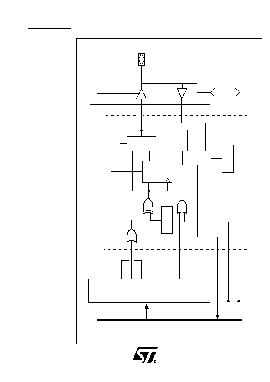
The circuit of a PE Macrocell is shown in Figure 11. There are 4 product terms from the
GPLD's AND ARRAY as input to the macrocell. Users can select the polarity of the output
and configure the macrocell to operate as:
t
Registered Output
Select output from D flip flop
t
Combinatorial Output
Select output from OR gate
t
GPLD Input
Use Port E pin as dedicated input
t
GPLD Output
Use Port E pin as dedicated output
t
GPLD I/O
Use Port E pin as bidirectional pin
t
Macrocell Feedback
Register feedback for state machine implementations or expander feedback from the
combinatorial output, to possibly expand the number of product terms available to
another macrocell.
In case of "Buried Feedback", where the output of the macrocell is not connected
to Port E pin, Port E can be configured to perform other user defined I/O functions.
If pins PE0 and PE1 are used as bus control signal inputs (ALE, PSEN/BHE), the
corresponding macrocells' feedbacks are disabled. The bus control signals are
connected to the ZPLD Input Bus.
The two global product terms assigned for asynchronous clear (PE.RE) and preset (PE.PR)
are mainly for proper PE Macrocell initialization.
The macrocell flip-flop can also be cleared during reset by MACRO-RST, if such an option
is chosen. The clock source is always the input clock CLKIN.
PSD5XX Family
24
Figure 10. PE Macrocell Block Diagram
AND ARRAY
MC0 PE0
MC1
PE1
MC7 PE
7
MACRO .OUT
PE0 ≠ INPUT
MACRO .OUT
PE1 ≠ INPUT
MACRO .OUT
PE7≠ INPUT
PT
PE0
PT
PE1
PT
PE7
PE .PR
PE .RE
PE .OE
CLKIN
MACRO ≠ RST
PORT E I/O CELLS
PE MACROCELL
The PSD5XX
Architecture
(cont.)
PSD5XX Family
25
Figure 11. PE Macrocell
DQ
PT
PT
PT
PT
AND
ARRAY
POLARITY
SELECT
PLD≠
IN
SELECT
C
PR
MUX
MUX
PE .OE
PE .PR
PT
PE .RE
PEi
MACRO
≠
RST
NOTE: i = 7 to 0
CLKIN
MACRO .OUT
I/O PIN
PEi
PORT E
INTERNAL
ADDRESS/DATA
BUS
PEi
≠
INPUT
COMB
/
REG
SELECT
ZPLD
BUS
The PSD5XX
Architecture
(cont.)

PSD5XX Family
26
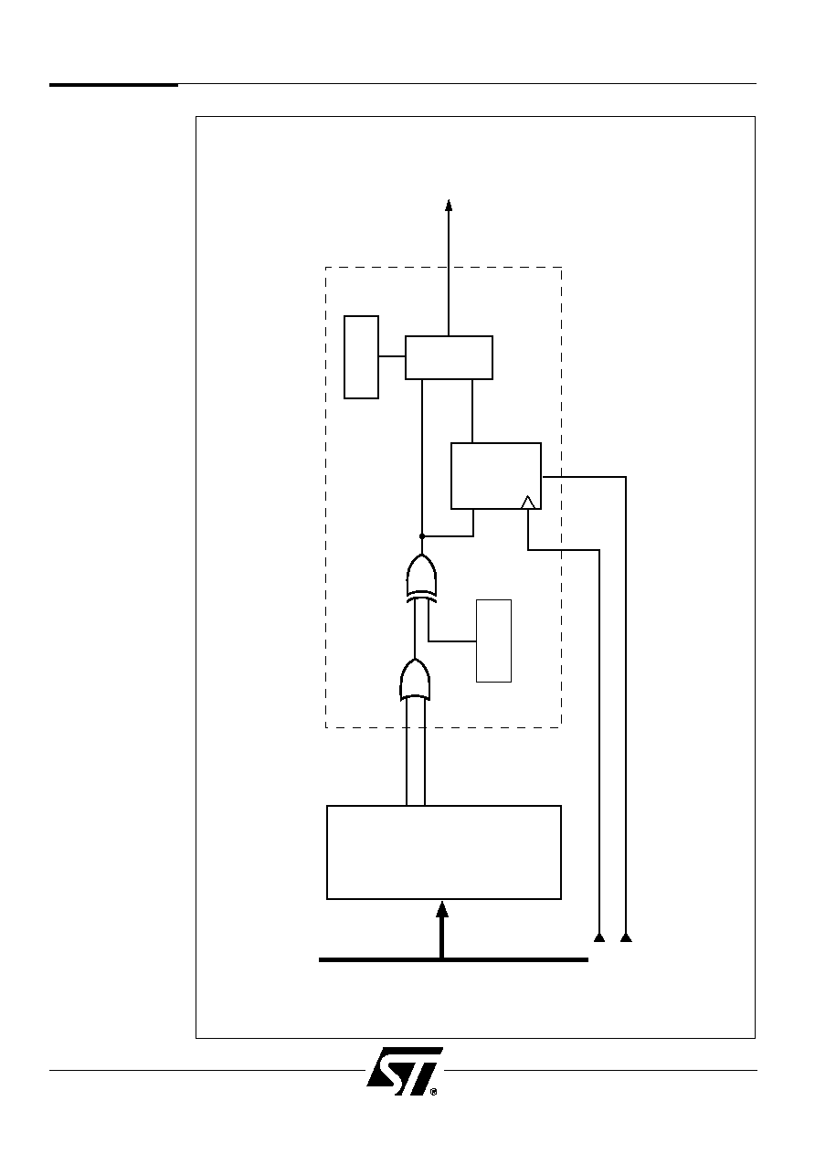
9.1.3 The PPLD
The Peripheral Programmable Logic Device (PPLD) provides a powerful mechanism for
the user to control the operations of the Counter/Timer and Interrupt Controller. Figure 12 is
the PPLD block diagram. There are six Peripheral Macrocells, four are dedicated to the
Counter/Timer, and two to the Interrupt Controller.
The outputs from the four Peripheral Macrocells, MC2TMR[3:0], are used as
load/store/enable inputs to the Counter/Timer (multiplexed with pin inputs TIMER[3:0] _IN).
The remaining two macrocell outputs (MC2INT[6:7] ), together with two other product terms
(PT2INT4, PT2INT5), can generate up to 4 user defined interrupts to the Interrupt
Controller. The watch-dog output of the Timer (WDOG2PLD) and Interrupt Controller
(INTR2PLD) are available as inputs to the ZPLD's AND ARRAY.
The structure of a Peripheral Macrocell is shown in Figure 13. The cell has two product term
inputs from the AND ARRAY. The user can select the registered or combinatorial output of
the macrocell, as well as the output polarity. The registers are clocked by the CLKIN clock,
and are cleared by the RESET input during power up.
9.1.4 The ZPLD Power Management
The ZPLD implements a Zero Power Mode, which provides considerable power savings
for low to medium frequency operations. To enable this feature, the ZPLD Turbo bit in the
Power Management Mode Register 0 (PMMR0) has to be turned off.
If none of the 61 inputs to the ZPLD are switching for a time period of 70ns, the ZPLD puts
itself into Zero Power Mode and the current consumption is minimal. The ZPLD will resume
normal operation as soon as one or more of the inputs change state.
Two other features of the ZPLD provide additional power savings:
1. Clock Disable:
Users can disable the clock input to the ZPLD and/or macrocells, thereby reducing AC
power consumption.
2. Product Term Disable:
Unused product terms in the ZPLD are disabled by the PSDsoft Software automatically
for further power savings.
The ZPLD power configuration is described in the Power Management Unit section.
The PSD5XX
Architecture
(cont.)

PSD5XX Family
27
Figure 12. PPLD Block Diagram
PORT
E
MACROCELLS
(4)
MACROCELLS
(2)
COUNTER/
TIMER
INTERRUPT
CONTROLLER
AND ARRAY
TIMER
[ 3 : 0
] ≠
IN
TC
[ 3 : 0
]
TC
[ 3 : 0
]
MC2TMR
[ 3 : 0
]
WDOG2PLD
INTR2PLD
PT2INT4
PT2INT5
MC2INT6
MC2INT7
PT (8)
PT (4 )
PT
PT
MUX
The PSD5XX
Architecture
(cont.)
PSD5XX Family
28
Figure 13. Peripheral Macrocell
DQ
PT
PT
AND
ARRAY
POLARITY
SELECT
COMB
/
REG
SELECT
C
MUX
PT0
PT1
CLKIN
RESET
TO TIMER OR
INTERRUPT
CONTROLLER
ZPLD
BUS
The PSD5XX
Architecture
(cont.)
PSD5XX Family
29
9.2
Bus
Interface
The Bus Interface is very flexible and can be configured to interface to most
microcontrollers with no glue logic. Table 4 lists some of the bus types to which the Bus
Interface is able to interface.
9.2.1 Bus Interface Configuration
The Bus Interface Logic is user configurable. The type of bus interface is specified by
the user in the PSDsoft software (PSD configuration). The bus control input pins have
multi-function capabilities. By choosing the right configuration, the PSD5XX is able to
interface to most microcontrollers, including the ones listed in Table 4. In Table 5, the
names of the bus control input signal pins and their multiple functions are shown. For
example, Pin PE0 can be configured by the PSD configuration software to perform any one
of the five functions. Examples on the interface between the PSD5XX and some typical
microcontrollers are shown in following sections.
Pin Name
Pin
Pin
Pin
Pin
Pin
Function
Function
Function
Function
Function
1
2
3
4
5
RD RD
E
DS
LDS
WR
WR
R/W
WRL
PE0
BHE
PSEN
WRH
UDS
SIZ0
PE1
ALE
AD0
A0
BLE
Table 5. Alternate Pin Functions
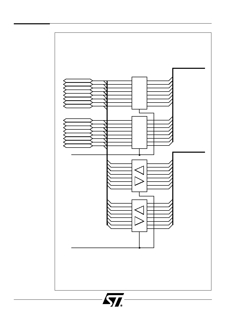
9.2.2 PSD5XX Interface To a Multiplexed Bus
Figure 14 shows a typical connection to a microcontroller with a multiplexed bus. The ADIO
port of the PSD5XX is connected directly to the microcontroller address/data bus
(AD0-AD15 for 16 bit bus). The ALE input signal latches the address lines internally. In a
read bus cycle, data is driven out through the ADIO Port transceivers after the specified
access time. The internal ADIO Port connection for a 16 bit multiplexed bus is shown in
Figure 15. The ADIO port is in tri-state mode if none of the PSD5XX internal devices are
selected.
Multiplexed
Data Bus
Bus Control
Microcontroller
Width
Signals
Mux
8
WR, RD, PSEN, A0
8031/80C51
Mux/Non-mux
8/16
R/W, E, BHE, A0
68HC11
Mux
8/16
WR, RD, BHE, A0
80C196/80C186
Mux
16
WRL, RD, WRH, A0
80C196SP
Non-mux
16
R/W, LDS, UDS
68302
Non-mux
8/16
R/W, DS, SIZ0, A0
68340
Non-mux
16
R/W, DS, BHE, BLE
68330, 68331
Non-mux
8
RD, WR
68HC05C
Non-mux
16
R/W, E, LSTRB, A0
68HC12
Non-mux
16 R/W,
DS
68HC16
Table 4. Typical Microcontroller Bus Types

PSD5XX Family
30
9.2.3 PSD5XX Interface To Non-Multiplexed Bus
Figure 16 shows a PSD5XX interfacing to a microcontroller with a non-multiplexed
address/data bus. The address bus is connected to the ADIO Port, and the data bus is
connected to Port C and/or Port D, depending on the bus width. There is no need for the
ADIO Port to latch the address internally, but the user is offered the option to do so in the
PSD5XX PSDsoft Software. The data ports are in tri-state mode when the PSD5XX is not
accessed by the microcontroller.
Bus
Interface
(Cont.)
9.2.4 Data Byte Enable
Microcontrollers have different data byte orientations with regard to the data bus. The
following tables show how the PSD5XX handles the byte enable under different bus
configurations. Even byte refers to locations with address A0 equal to "0", and odd byte as
locations with A0 equal to "1".
BHE
A0
D7 ≠ D0
X
0
Even Byte
X
1
Odd Byte
Table 6. 8-Bit Data Bus
Table 7. 16-Bit Data Bus With BHE
BHE
A0
D15 ≠ D8
D7 ≠ D0
0
0
Odd byte
Even byte
0
1
Odd byte
≠
1
0
≠
Even byte
WRH
WRL
D15 ≠ D8
D7 ≠ D0
0
0
Odd byte
Even byte
0
1
Odd byte
≠
1
0
≠
Even byte
Table 8. 16-Bit Data Bus With WRH and WRL
SIZ0
A0
D15 ≠ D8
D7 ≠ D0
0
0
Even byte
Odd byte
1
0
Even byte
≠
1
1
≠
Odd byte
Table 9. 16-Bit Data Bus With SIZ0, A0
LDS
UDS (A0)
D15 ≠ D8
D7 ≠ D0
0
0
Even byte
Odd byte
1
0
Even byte
≠
0
1
≠
Odd byte
Table 10. 16-Bit Data Bus With UDS, LDS

PSD5XX Family
31
Figure 14. Bus Interface ≠ Multiplexed Bus, 8 or 16-Bit Data Bus
MICRO-
CONTROLLER
AD ≠
[ 7:0
]
AD ≠
[ 15 : 8
]
(
A ≠
[ 15 : 8
]
)
A ≠
[ 7:0
]
A ≠
[ 15 : 8
]
(OPTIONAL)
(OPTIONAL)
ADIO
PORT
PORT E
WR
RD
RST
CSI
BHE
ALE
PORT C
PORT D
PORT A
PORT B
PSD5XX
Bus
Interface
(Cont.)
AD0
AD1
AD2
AD3
AD4
AD5
AD6
AD7
AD8
AD9
AD10
AD11
AD12
AD13
AD14
AD15
AD0
AD1
AD2
AD3
AD4
AD5
AD6
AD7
AD8
AD9
AD10
AD11
AD12
AD13
AD14
AD15
A0
A1
A2
A3
A4
A5
A6
A7
A8
A9
A10
A11
A12
A13
A14
A15
D0
D1
D2
D3
D4
D5
D6
D7
D8
D9
D10
D11
D12
D13
D14
D15
ADIO≠0
ADIO≠1
ADIO≠2
ADIO≠3
ADIO≠4
ADIO≠5
ADIO≠6
ADIO≠7
ADIO≠8
ADIO≠9
ADIO≠10
ADIO≠11
ADIO≠12
ADIO≠13
ADIO≠14
ADIO≠15
R_W
ALE /AS
PSD5XX
INTERNAL
ADDRESS BUS
PSD5XX
INTERNAL
DATA BUS
LATCH
G
LATCH
G
PSD5XX Family
32
Figure 15. ADIO Port, 16-Bit Multiplexed Bus Interface
Bus
Interface
(Cont.)
PSD5XX Family
33
Figure 16. Bus Interface ≠ Non-Multiplexed, 8 or 16-Bit Data
MICRO-
CONTROLLER
D ≠
[ 15 : 0
]
A ≠
[ 15 : 0
]
D ≠
[ 15 : 8
]
D ≠
[ 7 : 0
]
A
[ 23
:16
]
(OPTIONAL)
ADIO
PORT
PORT E
WR
RD
RST
CSI
BHE
ALE
PORT C
PORT D
PORT A
PORT B
PSD5XX
16-BIT DATA ONLY
Bus
Interface
(Cont.)

PSD5XX Family
34
9.2.5 Optional Features
The PSD5XX provides two optional features to add flexibility to the Bus Interface:
1. Address In
Port A can be configured as high order address (A16-A23) inputs to the ZPLD for
EPROM or other decoding. Inputs are latched by ALE/AS if Multiplexed Bus is selected.
Other ports can be configured as address input ports for the ZPLD. These inputs should
not be used for EPROM decoding and are not latched internally.
2. Address Out
For multiplexed bus only. Latched address lines A0-A15 are available on
Port A, B, C, D, or E.
Details on the optional features are described in the I/O Port section.
Bus
Interface
(Cont.)
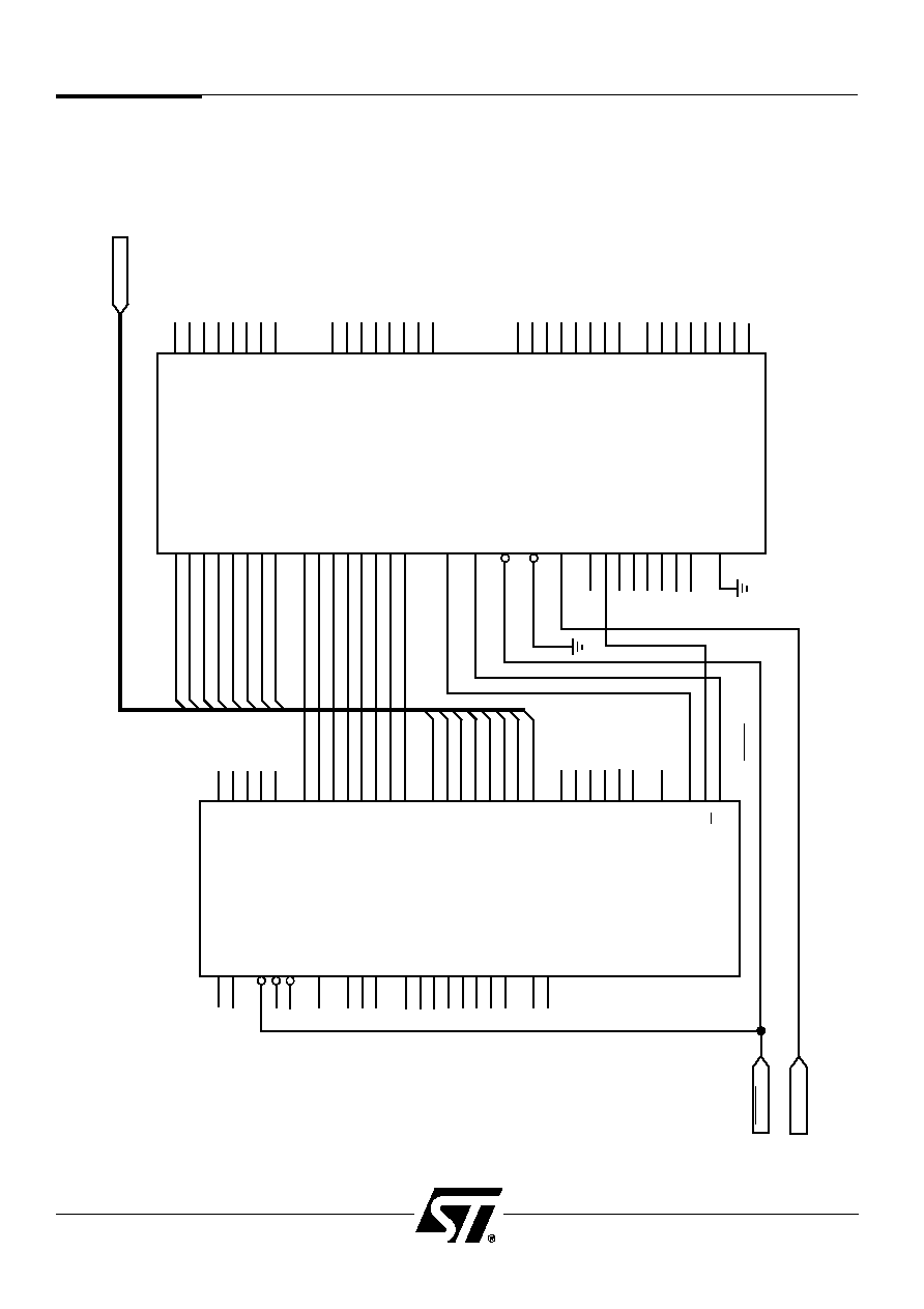
9.2.6 Bus Interface Examples
The next four figures show the PSD5XX interfacing with some popular microcontrollers.
The examples show only the basic bus connections; some of the pin names on the
PSD5XX parts change to reflect the actual pin functions.
Figure 17 shows an interface to the 80C31. The 80C31 has a 16 bit address bus and an
8-bit data bus. The lower address byte is multiplexed with the data bus. The RD and WR
signals are used for accessing the data memory (SRAM) and the PSEN signal is for reading
program memory (EPROM). The ALE signal is active high and is used to latch the address
internally. Port C provides latched address outputs A[7:0]. Ports A, B, D, and E (PE2-PE7)
can be configured to perform other functions. The RSTOUT reset to the 80C31 is generated
by the ZPLD from the RESET input. This configuration eliminates any reset race condition
between the 80C31 and the PSD5XX.
Figure 18 shows the 68HC11 interface, which is similar to the 80C31 except the PSD5XX
generates internal RD and WR from the 68HC11's E and R/W signals.
In Figure 19, the Intel 80C196 microcontroller is interfaced to the PSD5XX. The 80C196
has a multiplexed 16-bit address and data bus. The BHE signal is used for data byte
selection. Ports C and D are used as output ports for latched address A[15:0]. Pins PE6
and PE7 can be programmed as ZPLD outputs to provide the READY and BUSWIDTH
control signals to the 80C196.
Figure 20 shows Motorola's MC68331 interfacing to the PSD5XX. The MC68331 has a
16-bit data bus and a 24-bit address bus. D15-D8 from the MC68331 are connected to
Port D, and D7 ≠ D0 are connected to Port C.

PSD5XX Family
35
Figure 17. Interfacing PSD5XX With 80C31
E
A/V
P
X1
X2
RESET
INT0
INT1
T0
T1
P1 . 0
P1 . 1
P1 . 2
P1 . 3
P1 . 4
P1 . 5
P1 . 6
P1 . 7
AD0
/A0
AD1/A1
AD2
/A2
AD3
/A3
AD4
/A4
AD5
/A5
AD6
/A6
AD7/A7
AD8
/A8
AD9
/A9
AD10
/A10
AD11/A11
AD12
/A12
AD13
/A13
AD14
/A14
AD15
/A15
RD
WR
RESET
CSI
CLKIN
PE0
/
PSEN
PE1
/ALE
PE2
PE3
PE4
PE5
PE6
PE7
VSTDBY
P0.0
P0.1
P0.2
P0.3
P0.4
P0.5
P0.6
P0.7
P2.0
P2.1
P2.2
P2.3
P2.4
P2.5
P2.6
P2.7
RD
WR
PSEN
A
L
E/P
TXD
RXD
PC0
PC1
PC2
PC3
PC4
PC5
PC6
PC7
PD0
PD1
PD2
PD3
PD4
PD5
PD6
PD7
PA0
PA1
PA2
PA3
PA4
PA5
PA6
PA7
PB0
PB1
PB2
PB3
PB4
PB5
PB6
PB7
31
19
18
9
12
13
14
15
1
2
3
4
5
6
7
8
39
38
37
36
35
34
33
32
21
22
23
24
25
26
27
28
17
16
29
30
11
10
17
16
15
14
13
12
11
10
60
59
58
57
56
55
54
53
27
26
25
24
23
22
21
20
50
49
48
47
46
45
44
43
AD0
AD1
AD2
AD3
AD4
AD5
AD6
AD7
A8
A9
A10
A11
A12
A13
A14
A15
9
8
7
6
5
4
3
2
68
67
66
65
64
63
62
61
41
29
40
39
42
38
37
36
34
33
32
31
30
28
80C31
AD
[ 7:0
]
AD
[ 7:0
]
RESET
RSTOUT
CLOCK
RESET
CLOCK
PSD5XX
RD
WR
PSEN
ALE
PSD5XX Family
36
Figure 18. Interfacing PSD5XX With 68HC11
XT
EX
RESET
IRQ
XIRQ
MODB
PA0
PA1
PA2
PE0
PE1
PE2
PE3
PE4
PE5
PE6
PE7
VRH
VRL
AD0
/A0
AD1/A1
AD2
/A2
AD3
/A3
AD4
/A4
AD5
/A5
AD6
/A6
AD7/A7
AD8
/A8
AD9
/A9
AD10
/A10
AD11/A11
AD12
/A12
AD13
/A13
AD14
/A14
AD15
/A15
E
R/W
RESET
CSI
CLKIN
PE0
PE1 / ALE
PE2
PE3
PE4
PE5
PE6
PE7
VSTDBY
PA3
PA4
PA5
PA6
PA7
PB0
PB1
PB2
PB3
PB4
PB5
PB6
PB7
PC0
PC1
PC2
PC3
PC4
PC5
PC6
PC7
PD0
PD1
PD2
PD3
PD4
PD5
MODA
E
AS
R/W
PC0
PC1
PC2
PC3
PC4
PC5
PC6
PC7
PD0
PD1
PD2
PD3
PD4
PD5
PD6
PD7
PA0
PA1
PA2
PA3
PA4
PA5
PA6
PA7
PB0
PB1
PB2
PB3
PB4
PB5
PB6
PB7
8
7
17
19
18
2
34
33
32
43
44
45
46
47
48
49
50
52
51
31
30
29
28
27
42
41
40
39
38
37
36
35
9
10
11
12
13
14
15
16
20
21
22
23
24
25
3
5
4
6
17
16
15
14
13
12
11
10
60
59
58
57
56
55
54
53
27
26
25
24
23
22
21
20
50
49
48
47
46
45
44
43
AD0
AD1
AD2
AD3
AD4
AD5
AD6
AD7
A8
A9
A10
A11
A12
A13
A14
A15
9
8
7
6
5
4
3
2
68
67
66
65
64
63
62
61
41
29
40
39
42
38
37
36
34
33
32
31
30
28
68HC11
RESET
PSD5XX
AD
[ 7 : 0
]
AD
[ 7 : 0
]
CLOCK
RESET
E
ALE
R/W
CLOCK
AD0
AD1
AD2
AD3
AD4
AD5
AD6
AD7

PSD5XX Family
37
Figure 19. Interfacing PSD5XX With 80C196
X1
NMI
READY
CDE
BUSWIDTH
RESET
ACH0
/
P0 . 0
ACH1
/
P0 . 1
ACH2
/
P0 . 2
ACH3
/
P0 . 3
ACH4
/
P0 . 4
ACH5
/
P0 . 5
PCS6
/
P0 . 6
PCS7/
P0 . 7
P2 . 0
/
TXD
P2 . 1
/
RXD
P2 . 2
/
EXINT
P2 . 3
/
T2CLK
P2 . 4
/
T2RST
P2 . 5
/
PWM
P2 . 6
/
T2UP ≠ DN
P2 . 7/
T2CAP
HSI .0
HSI .1
HSI .2 / HSO .4
HSI .3 / HSO .5
VREF
ANGND
EA
AD0
/A0
AD1
/A1
AD2
/A2
AD3
/A3
AD4
/A4
AD5
/A5
AD6
/A6
AD7/A7
AD8
/A8
AD9
/A9
AD10
/A10
AD11
/A11
AD12
/A12
AD13
/A13
AD14
/A14
AD15
/A15
RD
WR
RESET
CSI
CLKIN
PE0
/
BHE
PE1
/ALE
PE2
PE3
PE4
PE5
PE6
PE7
VSTDBY
X2
P3 . 0
/AD0
P3 . 1
/AD1
P3 . 2
/AD2
P3 . 3
/AD3
P3 . 4
/AD4
P3 . 5
/AD5
P3 . 6
/AD6
P3 . 7/AD7
P4 . 0
/AD8
P4 . 1
/AD9
P4 . 2
/AD10
P4 . 3
/AD11
P4 . 4
/AD12
P4 . 5
/AD13
P4 . 6
/AD14
P4 . 7/AD15
RD
WR
BHE
ALE
INST
CLKOUT
P1 .0
P1 .1
P1 .2
P1 .3
P1 .4
P1 .5
P1 .6
P1 .7
HSO .0
HSO .1
HSO .2
HSO .3
PC0
PC1
PC2
PC3
PC4
PC5
PC6
PC7
PD0
PD1
PD2
PD3
PD4
PD5
PD6
PD7
PA0
PA1
PA2
PA3
PA4
PA5
PA6
PA7
PB0
PB1
PB2
PB3
PB4
PB5
PB6
PB7
11
3
43
14
64
16
6
5
7
4
11
10
8
9
18
17
15
44
42
39
33
38
24
25
26
27
13
12
2
12
60
59
58
57
56
55
54
53
52
51
50
49
48
47
46
45
61
40
41
62
63
65
59
58
57
56
55
48
47
46
50
49
44
43
17
16
15
14
13
12
11
10
60
59
58
57
56
55
54
53
27
26
25
24
23
22
21
20
50
49
48
47
46
45
44
43
AD0
AD1
AD2
AD3
AD4
AD5
AD6
AD7
AD8
AD9
AD10
AD11
AD12
AD13
AD14
AD15
9
8
7
6
5
4
3
2
68
67
66
65
64
63
62
61
41
29
40
39
42
38
37
36
34
33
32
31
30
28
RESET
D
[ 15 : 0
]
D
[ 15 : 0
]
RESET
READY
BUSWIDTH
RD
WR
BHE
ALE
CLKOUT
PSD5XX
80C196
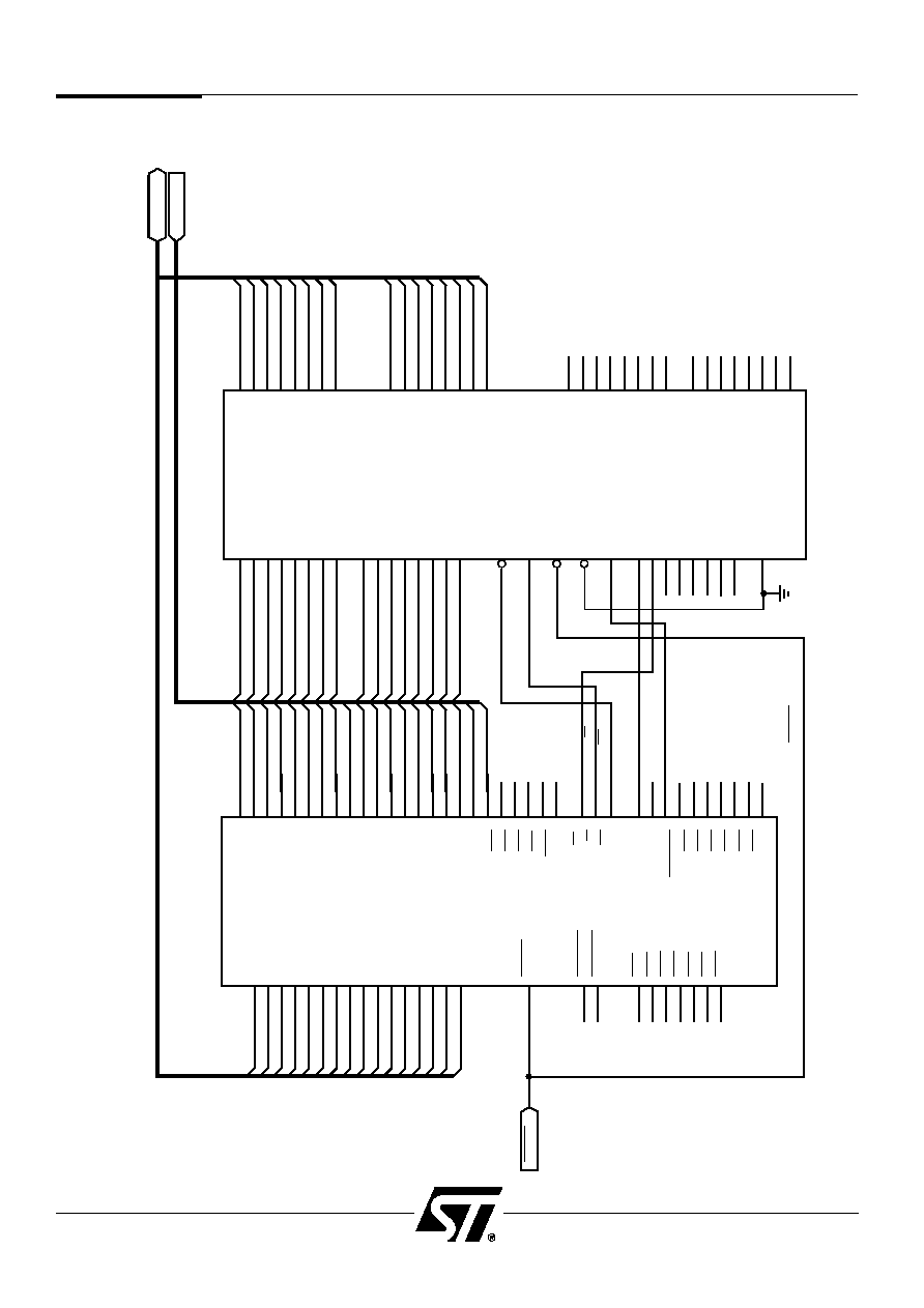
PSD5XX Family
38
Figure 20. Interfacing PSD5XX With Motorola 68331
D0
D1
D2
D3
D4
D5
D6
D7
D8
D9
D10
D11
D12
D13
D14
D15
RESET
DSACK0
DSACK1
IRQ1
IRQ2
IRQ3
IRQ4
IRQ5
IRQ6
IRQ7
AD0 / A0
AD1 / A1
AD2 / A2
AD3 / A3
AD4 / A4
AD5 / A5
AD6 / A6
AD7 / A7
AD8 / A8
AD9 / A9
AD10 / A10
AD11 / A11
AD12 / A12
AD13 / A13
AD14 / A14
AD15 / A15
DS
R /
W
RESET
CSI
CLKIN
PE0
/
SIZ0
PE1
/ALE
PE2
PE3
PE4
PE5
PE6
PE7
VSTDBY
A0
A1
A2
A3
A4
A5
A6
A7
A8
A9
A10
A11
A12
A13
A14
A15
A16
A17
A18
A19
≠
CS6
A20
≠
CS7
A21
≠
CS8
A22
≠
CS9
A23
≠
CS10
AS
R
≠
W
DS
SIZ0
SIZ1
CLKOUT
CSBOOT
BR
≠
CS0
BG
≠
CS1
BGACK≠
CS2
FC0
≠
CS3
FC1≠
CS4
FC2≠
CS5
PC0
PC1
PC2
PC3
PC4
PC5
PC6
PC7
PD0
PD1
PD2
PD3
PD4
PD5
PD6
PD7
PA0
PA1
PA2
PA3
PA4
PA5
PA6
PA7
PB0
PB1
PB2
PB3
PB4
PB5
PB6
PB7
D0 111
D1 110
D2 109
D3 108
D4 105
D5 104
D6 103
D7 102
D8 100
D9 99
D10 98
D11 97
D12 94
D13 93
D14 92
D15 91
68
89
88
77
76
75
74
73
72
71
D0 111
D1 110
D2 109
D3 108
D4 105
D5 104
D6 103
D7 102
D8 100
D9 99
D10 98
D11 97
D12 94
D13 93
D14 92
D15 91
68
89
88
77
76
75
74
73
72
71
90
20
21
22
23
24
25
26
27
30
31
32
33
35
36
37
38
41
42
121
122
123
124
125
82
79
85
81
80
66
112
113
114
115
118
119
120
17
16
15
14
13
12
11
10
60
59
58
57
56
55
54
53
27
26
25
24
23
22
21
20
50
49
48
47
46
45
44
43
A0
A1
A2
A3
A4
A5
A6
A7
A8
A9
A10
A11
A12
A13
A14
A15
A16
A17
A18
ALE
RW
DS
SIZ0
CLKOUT
D0
D1
D2
D3
D4
D5
D6
D7
D8
D9
D10
D11
D12
D13
D14
D15
A0
A1
A2
A3
A4
A5
A6
A7
A8
A9
A10
A11
A12
A13
A14
A15
9
8
7
6
5
4
3
2
68
67
66
65
64
63
62
61
41
29
40
39
42
38
37
36
34
33
32
31
30
28
RESET
D
[ 15 : 0
]
D
[ 15 : 0
]
A
[ 18 : 0
]
A
[ 18 : 0
]
RESET
PSD5XX
MC68331

PSD5XX Family
39
There are 5 programmable 8-bit I/O ports: Port A, Port B, Port C, Port D and Port E. These
ports all have multiple operating modes, depending on the configuration. Some of the basic
functions are providing input/output for the ZPLD, the Counter/Timer, or can be used for
standard I/O. Each port pin is individually configurable, thus enabling a single 8-bit port to
perform multiple functions. The I/O ports occupy 256 bytes of memory space as defined by
"CSIOP". Refer to the System Configuration section for I/O register address offset.
To set up the port configuration the user is required to:
1. Define I/O port chip select (CSIOP) in the ABEL file.
2. Initialize certain port configuration registers in the user's program and/or
3. Specify the configuration in the PSD5XX PSDsoft Software.
4. Unused input pins should be tied to V
CC
or GND.
The following is a description of the operating modes of the I/O ports. The functions of the
port registers are described in later sections.
9.3.1 Standard MCU I/O
The Standard MCU I/O Mode provides additional I/O capability to the microcontroller.
In this mode, the ports can perform standard I/O functions such as sensing or controlling
various external I/O devices. Operation options of this mode are as follows:
t
Configuration
1. Declare pins or signals which are used as I/O in the ABEL file (PSDsoft).
2. Set the bit or bits in the Control Register to "1".
3.
As Output Port
≠ Write output data to Data Out Register
≠ Set Direction Register to output mode
4.
As Input Port
≠ Set Direction Register to input mode
≠ Read input from Data In Register
The port remains an output or input port as long as the Direction Register is not changed.
9.3.2 PLD I/O
The PLD I/O mode enables the port to be configured as an input to the ZPLD, or as an
output from the GPLD macrocell. The output can be tri-stated with a control signal defined
by a product term from the ZPLD. This mode is configured by the user in the PSD5XX
PSDsoft Software, and is enabled upon power up. For a detailed description, see the
section on the ZPLD.
t
Configuration
1. Declare pins or signals in the ABEL file (PSDsoft)
2. Write logic equations in the ABEL file.
3. PSDcompiler maps the PLD function to the PSD.
9.3
I/O Ports

PSD5XX Family
40
9.3.3 Address Out
For microcontrollers with a multiplexed address/data bus, the I/O ports in Address-Out
mode are able to provide latched address outputs (A0 ≠ A15) to external devices. This
mode of operation requires the user to:
t
Configuration
1. Declare the pins used as address line outputs in the ABEL file PSDsoft.
2. Write "0" to the corresponding bit in the Control Register associated
with each I/O port.
3. Set the Direction Register to Output Mode.
9.3.4 Address In
1. For Port A ≠ as other address line (A2 ≠ A7 and A16 ≠ A23) inputs to the DPLD.
Additional address inputs included in the EPROM decoding must come from Port A.
The address inputs are latched internally by ALE/AS if Multiplexed Bus is specified in
PSDsoft.
2. For Ports C and D ≠ as adress inputs to the ZPLD for general decoding, should not be
used in EPROM decoding.
t
Configuration
1. Declare pins or signals used as Address In in the ABEL file (PSDsoft).
2. Write latch equations in the ABL file, e.g., A16.LE = ALE
3. Include latched address in logic equations.
9.3.5 Data Port
In this mode, the port is acting as a data bus port for a microcontroller which has a
non-multiplexed address/data bus. In this configuration, the Data Port is connected to the
data bus of the microcontroller and the ADIO port is connected to the address bus.
t
Configuration
Select the non-multiplexed bus option in PSD configuration (PSDsoft).
9.3.6 Special Function Out
This mode is per-pin configurable. When enabled, the special function assigned to the
particular pin is driven out. Special functions consist of Timer and Interrupt outputs.
t
Configuration
1. Specify the output function in the PSD configuration (PSDsoft).
2. PSD compiler assigns pins for the selected function.
3. Write "1" to the corresponding bit in the Special Function Register.
I/O Ports
(Cont.)
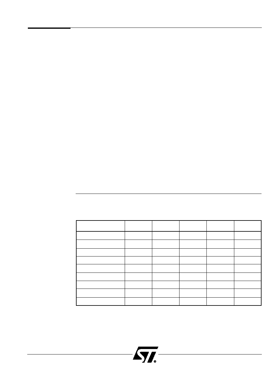
PSD5XX Family
41
9.3.7 Alternate Function In
This mode is per-pin configurable and enables the user to define the pins in Port E to
perform Alternate function. Alternate Function includes inputs to Counter/Timers and APD
clock.
t
Configuration
1. Select input functions in PSD configuration
2. PSD compiler assigns pins for the selected function.
9.3.8 Peripheral I/O
This mode enables the microcontroller to read or write to a peripheral though Port A.
When there is no read/write operation, Port A is tri-stated. One of the applications of
Peripheral I/O is in a DMA based design.
t
Configuration
1. Declare the pins used as Peripheral I/O in the ABEL file.
2. Write logic equations for PSEL0 and PSEL1.
3. Write a "1" to the PIO bit in the VM Register to activate the Peripheral I/O operation.
See the section on Peripheral I/O for a detailed description.
9.3.9 Open Drain Outputs
This mode enables the user to configure Port C and D pins as open drain outputs. CMOS
output is the default configuration. Writing "1" to the corresponding bit in the Open Drain
Register changes the pin to open drain output.
Port Mode
Port A
Port B
Port C
Port D
Port E
Standard MCU I/O
Yes
Yes
Yes
Yes
Yes
PLD I/O
Yes
Yes
Input Only
Input Only
Yes
Address Out
Yes
Yes
Yes
Yes
Yes
Address In
Yes
Yes
*
Yes
*
Yes
*
Yes
*
Data Port
Yes
Yes
Special Function Out
Yes
Yes
Yes
Alternate Function In
Yes
Peripheral I/O
Yes
Open Drain
Yes
Yes
*
For external decoding. Cannot be latched by ALE.
Table 11. Operating Modes of the I/O Ports
The following table summarizes the operating modes of the I/O ports. Not all functions are
available to every port.
I/O Ports
(Cont.)
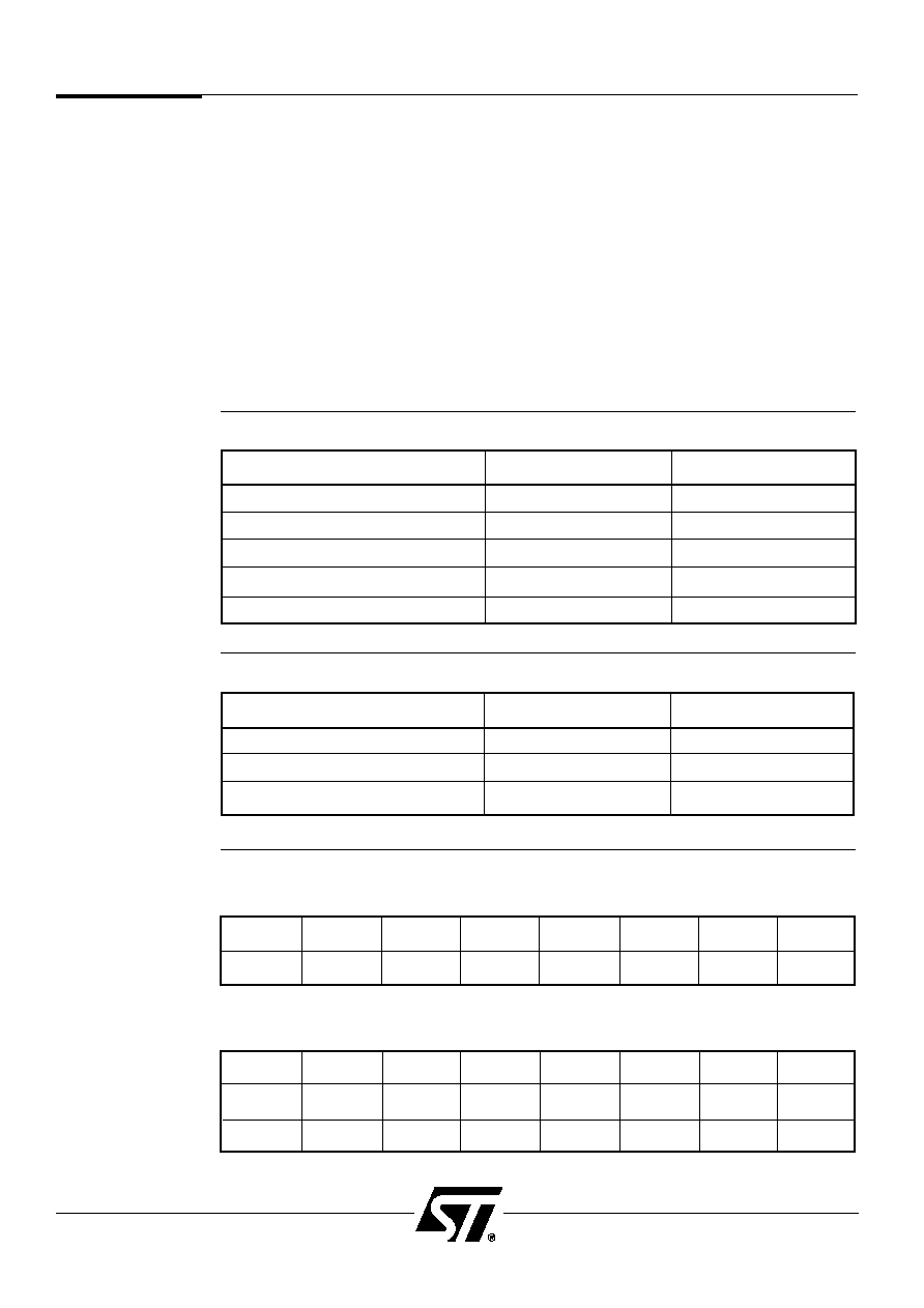
PSD5XX Family
42
9.3.10 Port Registers
There are two sets of registers per I/O port: the Port Configuration Registers (PCR) which
consist of four 8-bit registers; and the Port Data Registers (PDR) which include three 8-bit
registers. The PCR is used for setting up the port configuration, while the PDR enables the
microcontroller to write or read port data or status bits. Tables 12 and 13 show the names
and the registers and the ports to which they belong.
All the registers in the PCR and PDR are 8-bits wide and each bit is associated with a pin in
the I/O port. In Table 14, the LSB of the Data In Register of Port A is connected to pin PA0,
and the MSB is connected to PA7. This pin configuration also applies to other registers and
ports. For example, in the Direction Register of Port A, writing a hex value of 07 to the
register configures pins PA0 ≠ PA2 as output pins, while PA3 ≠ PA7 remain as input pins.
Registers can be accessed by the microcontroller during normal read/write bus cycles.
The I/O address offset of the registers are listed in the System Configuration section.
I/O Ports
(Cont.)
Register Name
Port
Write/Read
Control Register
A,B,C,D,E
Write/Read
Direction Register
A,B,C,D,E
Write/Read
Open Drain Register
C,D
Write/Read
Special Function Register
A,B,E
Write/Read
PLD ≠ I/O Register
A,B,E
Read
Table 12. Port Configuration Registers (PCR)
Register Name
Port
Read/Write
Data In Register
A,B,C,D,E
Read
Data Out Register
A,B,C,D,E
Write/Read
Macrocell Out Register
A,B,E
Read
Table 13. Port Data Registers (PDR)
Bit 7
Bit 6
Bit 5
Bit 4
Bit 3
Bit 2
Bit 1
Bit 0
PA7 Pin
PA6 Pin
PA5 Pin
PA4 Pin
PA3 Pin
PA2 Pin
PA1 Pin
PA0 Pin
Table 14.
Data In Register ≠ Port A
Bit 7
Bit 6
Bit 5
Bit 4
Bit 3
Bit 2
Bit 1
Bit 0
PA7 Pin
PA6 Pin
PA5 Pin
PA4 Pin
PA3 Pin
PA2 Pin
PA1 Pin
PA0 Pin
= 0
= 0
= 0
= 0
= 0
= 1
= 1
= 1
Direction Register ≠ Port A
( Example: Pins PA0 ≠ PA2 as Output, PA3 ≠ PA7 as Input)

PSD5XX Family
43
Control Register
This register is used in both Standard MCU I/O Mode and Address Out modes. For setting
a Standard MCU I/O Mode, a "1" must be written to the corresponding bit in the register.
Writing a "0" to the register is required for the Address Out mode. The register has a default
value of "0" after reset.
Direction Register
This register is used to control the direction of data flow in the I/O ports. Writing a "1" to
the corresponding bit in the register configures the port to be an output port, and a "0"
forces the port to be an input port. The I/O configuration of the port pins can be determined
by reading the Direction Register. After reset, the pins are in input mode.
Open Drain Register
This register determines whether the output pin driver of Port C or D is a CMOS driver or
an Open Drain driver. Writing a "0" to the register selects a CMOS driver, while a "1" selects
an Open Drain driver.
Special Function Register
Writing a "1" bit to this register sets up the corresponding pin to operate in Special Function
Out mode.
PLD ≠ I/O Register
This is a read only status register. Reading a "1" indicates the corresponding pin is
configured as a PLD pin. A "0" indicates the pin is an I/O pin.
Data In Register
This register is used in the Standard MCU I/O Mode configuration to read the input pins.
Data Out Register
This register holds the output data in the Standard MCU I/O Mode. The contents of the
register can also be read.
Macrocell Out Register
This register enables the user to read the outputs of the GPLD macrocell (PA, PB, and PE
macrocells).
I/O Register Address Offset
The I/O Register can be accessed by the microcontroller during normal read/write bus
cycles. The address of a register is defined as:
CSIOP + register address offset
The CSIOP is the base address that is defined in the ABEL file and occupies a 256 byte
space. The register address offset lies within this 256 byte space. Tables 15 and 15a are
the address offset of the registers.
I/O Ports
(Cont.)

PSD5XX Family
44
Table 15a. Register Address Offset
(For 16-bit Motorola Microcontrollers in 16-bit mode. Use Table 15 if 8-bit mode is selected.)
Address Offset
Register Name
Port A
Port B
Port C
Port D
Port E
Data In
00
01
10
11
20
Control
02
03
12
13
22
Data Out
04
05
14
15
24
Direction
06
07
16
17
26
Open Drain
18
19
Special Function
08
09
28
PLD ≠ I/O
0A
0B
2A
Macrocell Out
0C
0D
2C
Table 15. Register Address Offset
I/O Ports
(Cont.)
Address Offset
Register Name
Port A
Port B
Port C
Port D
Port E
Data In
01
00
11
10
21
Control
03
02
13
12
23
Data Out
05
04
15
14
25
Direction
07
06
17
16
27
Open Drain
19
18
Special Function
09
08
29
PLD ≠ I/O
0B
0A
2B
Macrocell Out
0D
0C
2D

PSD5XX Family
45
9.3.11 Port A ≠ Functionality and Structure
Port A is the most flexible of all the I/O ports. It can be configured to perform one or more
of the following functions:
t
Standard MCU I/O Mode
t
PLD I/O
t
Address Out ≠ latched address lines assigned to pins PA[0-7]
t
Address In ≠ input port for other lines, inputs can be latched by ALE.
t
Special Function Out ≠ pins PA0 ≠ PA3 can be configured as dedicated timer outputs.
t
Peripheral I/O
Figure 21 shows the structure of a Port A pin. If the pin is configured as an output port, the
multiplexer selects one of its four inputs as output. If the pin is configured as an input, the
input connects to :
1. Data In Register as input in Standard MCU I/O Mode
or
2. PA Macrocell as PLD input
or
3. PA Macrocell as Address In input (latched for multiplexed bus).
9.3.12 Port B ≠ Functionality and Structure
Port B is similar to Port A in structure. It can be configured to perform one or more of the
following functions:
t
Standard MCU I/O Mode
t
PLD I/O
t
Address Out ≠ address lines A[0-7] for 8-bit multiplexed bus, or address lines
A[8-15] for 16-bit multiplexed bus are assigned to pins PB[0-7].
t
Special Function Out ≠ pins PB0 - PB3 are configured as dedicated Timer outputs.
Figure 22 shows the structure of a Port B pin. If the pin is configured as an output port, the
multiplexer selects one of its four inputs as output. If the pin is configured as input, the input
connects to :
t
Data In Register as input in Standard MCU I/O Mode
or
t
PB Macrocell as PLD input
I/O Ports
(Cont.)
PSD5XX Family
46
Figure 21. Port A Pin Structure
MUX
PDR
PORT A PIN
DQ
D
G
Q
DQ
CONTROL
GPLD
≠
INPUT
PCR
ALE
WR
ALE
PA . OE
SPECIAL FUNC.
GPLD
≠
OUTPUT
ALE
WR
INTERNAL
ADDRESS /
DATA BUS
DATA OUT
ADDRESS
PCR
DIR. REG.
LATCH
A
[ 0 ≠ 7
]
The PSD5XX
Architecture
(cont.)

PSD5XX Family
47
Figure 22. Port B Pin Structure
MUX
PDR
PORT B
PIN
DQ
D
G
Q
DQ
CONTROL
GPLD
≠
INPUT
PCR
WR
ALE
PB .OE
SPECIAL FUNC.
GPLD
≠
OUTPUT
ALE
WR
INTERNAL
ADDRESS /
DATA BUS
DATA OUT
ADDRESS
PCR
DIR. REG.
A[0 ≠ 7]
OR
A[8 ≠ 15]
The PSD5XX
Architecture
(cont.)

PSD5XX Family
48
9.3.13 Port C and Port D ≠ Functionality and Structure
Port C and D are identical in function and structure and each can be configured to perform
one or more of the following operating modes:
t
Standard MCU I/O Mode
t
PLD Input ≠ direct input to ZPLD
t
Address Out ≠ latched address outputs
≠ Port C: A[0-7] are asigned to pins PC[0-7]
≠ Port D: A[0-7] for 8-bit multiplexed bus, or A[8-15] for 16-bit multiplexed bus are
assigned to pins PD[0-7]
t
Data Port
≠ Port C: D[0-7] for 8-bit non-multiplexed bus
≠ Port D: D[8-15] for 16-bit non-multiplexed bus
t
Open Drain ≠ select CMOS or Open Drain driver
Figures 23 and 24 show the structure of a Port C or D pin. If the pin is configured as output
port, the multiplexer selects one of the two inputs as output. If the pin is configured as input,
the input connects to :
t
Data In Register as input in the Standard MCU I/O Mode
or
t
ZPLD input
9.3.14 Port E ≠ Functionality and Structure
Port E can be configured to perform one or more of the following functions:
t
Standard MCU I/O Mode
t
PLD I/O
t
Address Out ≠ latched address lines A[0-7] are assigned to pins PE[0-7].
t
Special Function Out ≠ in this mode, Port E pin is configured as an output port for the
following signals:
PE2 ≠ INTERRUPT ≠ interrupt output from Interrupt Controller
PE4 ≠ Terminal Count output, Timer0
PE5 ≠ Terminal Count output, Timer1
PE6 ≠ Terminal Count output, Timer2
PE7 ≠ Terminal Count output, Timer3
t
Alternate Function In ≠ in this mode, the inputs to Port E pins are:
PE0 ≠ BHE/ or PSEN/ or WRH/ or UDS/ or SIZ0
PE1 ≠ ALE
PE3 ≠ TIMER0-IN
:load/store/enable/ disable input to Timer 0
PE4 ≠ TIMER1-IN
:load/store/enable/disable input to Timer 1
PE5 ≠ TIMER2-IN
:load/store/enable/disable input to Timer 2
PE6 ≠ TIMER3-IN
:load/store/enable/disable input to Timer 3
PE7 ≠ APD CLK
:clock input for Automatic Power Down Counter
Figure 25 shows the structure of a Port E pin. The Control Logic block selects one of four
sources through the multiplexer for pin output. If the pin is configured as input, the input
goes to:
t
Data In Register as input in Standard MCU I/O Mode
or
t
PE Macrocell as PLD input
or
t
Alternate Function In
I/O Ports
(Cont.)
PSD5XX Family
49
Figure 23. Port C Pin Structure
MUX
PDR
PORT C PIN
DQ
D
G
Q
DQ
CONTROL
GPLD
≠
INPUT
*
PCR
WR
ALE
ALE
WR
DATA
*
INTERNAL
ADDRESS /
DATA BUS
DATA OUT
ADDRESS
PCR
DIR. REG.
D
[ 0≠
7
]
A
[ 0≠
7
]
*
Data Bus D [0≠7] is not connected to GPLD≠Input.
I/O Ports
(Cont.)
PSD5XX Family
50
Figure 24. Port D Pin Structure
MUX
PDR
PORT D PIN
DQ
D
G
Q
DQ
CONTROL
GPLD
≠
INPUT
*
PCR
WR
ALE
ALE
WR
DATA
*
INTERNAL
ADDRESS /
DATA BUS
DATA OUT
ADDRESS
PCR
DIR. REG.
D [8
≠15]
A
[ 0≠
7
]
OR
A [8
≠15]
*
Data Bus D [8
≠15
] is not connected to GPLD≠Input.
I/O Ports
(Cont.)

PSD5XX Family
51
Figure 25. Port E Pin Structure
MUX
PDR
PORT E
PIN
DQ
D
G
Q
DQ
CONTROL
GPLD
≠
INPUT
ALT
FUNC. IN
PCR
WR
ALE
PE . OE
SPECIAL FUNC.
GPLD
≠
OUTPUT
ALE
WR
INTERNAL
ADDRESS /
DATA BUS
DATA OUT
ADDRESS
PCR
DIR. REG.
I/O Ports
(Cont.)

PSD5XX Family
52
The PSD5XX provides EPROM memory for code storage and SRAM memory for scratch
pad usage. Chip selects for the memory blocks come from the DPLD decoding logic and are
defined by the user in the PSDsoft Software. Figure 26 shows the organization of the
Memory Block.
All PSD families use Zero-power memory techniques that place memory into standby
between MCU accesses. The memory becomes active briefly after an address transition,
then delivers new data to the outputs, latches the outputs, and returns to standby. This is
done automatically and the designer has to do nothing special to benefit from this feature.
9.4.1 EPROM
The PSD5XX provides three EPROM densities: 256Kbit, 512Kbit or 1Mbit. The EPROM
is divided into four 8K, 16K or 32K byte blocks. Each block has its own chip select signals
(ES0 ≠ ES3). The EPROM can be configured as 32K x 8, 64K x 8 or 128K x 8 for
microcontrollers with an 8-bit data bus. For 16-bit data buses, the EPROM is configured as
16K x 16, 32K x 16, or 64K x 16.
9.4.2 SRAM
The SRAM has 16Kbits of memory, organized as 2K x 8 or 1K x 16. The SRAM is enabled
by the chip select signal RS0 from the DPLD. The SRAM has a battery back-up (STBY)
mode. This back-up mode is invoked when the V
CC
voltage drops under the VSTBY voltage
by 0.6 V. The VSTBY voltage is connected only to the SRAM and cannot be lower than
2.7 volts. The SRAM Data Retention voltage is 2 volts.
9.4.3 Memory Select Map
The EPROM and SRAM chip select equations are defined in the ABEL file in terms of
address and other DPLD inputs. The memory space for the EPROM chip select
(ES0 ≠ ES3) should not be larger than the EPROM block (8KB, 16KB or 32KB) it is
selecting.
The following rules govern how the internal PSD5XX memory selects/space are defined:
t
The EPROM blocks address space cannot overlap
t
SRAM, internal I/O and Peripheral I/O space cannot overlap
t
SRAM, internal I/O and Peripheral I/O space can overlap EPROM space, with priority
given to SRAM or I/O. The portion of EPROM which is overlapped cannot be accessed.
The Peripheral I/O space refers to memory space occupied by peripherals when Port A is
configured in the Peripheral I/O Mode.
9.4
Memory
Block
PSD5XX Family
53
Figure 26. Memory Block Diagram (128KB EPROM)
ES0
ES1
ES2
ES3
16K
x
8
16K
x
8
1K
x
8
1K
x
8
16K
x
8
16K
x
8
16K
x
8
16K
x
8
16K
x
8
16K
x
8
SRAM BLOCK
RS0
ODD BYTE
ODD BYTE
D
[ 8 ≠ 15
]
EVEN BYTE
D
[ 0 ≠ 7
]
EPROM BLOCKS
Memory
Block
(Cont.)

PSD5XX Family
54
9.4.4 Memory Select Map For 8031 Application
The 8031 family of microcontrollers has separate code memory space and data memory
space. This feature requires a different Memory Select Map. Two modes of operation are
provided for 8031 applications. The selection of the modes is specified in the PSD5XX
PSDsoft Software (PSDconfiguration):
t
Separate Space Mode
In this mode, the PSEN signal is used to access code from EPROM, and the RD signal
is used to access data from SRAM. The code memory space is separated from the data
memory space.
t
Combined Space Mode
In this mode, the EPROM can be accessed by PSEN or RD. The EPROM is used for
code and data storage. The memory block's address space cannot overlap.
If data and code memory blocks must overlap each other, the RD signal can be included as
an additional address input in generating the EPROM chip select signals (ES0 ≠ ES3). In
this case the EPROM access time is from the RD valid to data valid. Figures 27a and 27b
show the memory configuration in the two modes.
In some applications it is desirable to execute program codes in SRAM. The PSD5XX
provides this option by enabling PSEN to access SRAM. To activate this option, the
SRCODE bit of the VM Register must be set to "1" (see Table 16). SRAM space can
overlap EPROM space and has priority when PSEN is used.
Bit 7
Bit 6
Bit 5
Bit 4
Bit 3
Bit 2
Bit 1
Bit 0
*
*
*
*
*
*
SRCODE
PIO
1 = ON
1 = ON
*
= Reserved for future use, bits set to zero.
Table 16. VM Register
Memory
Block
(Cont.)
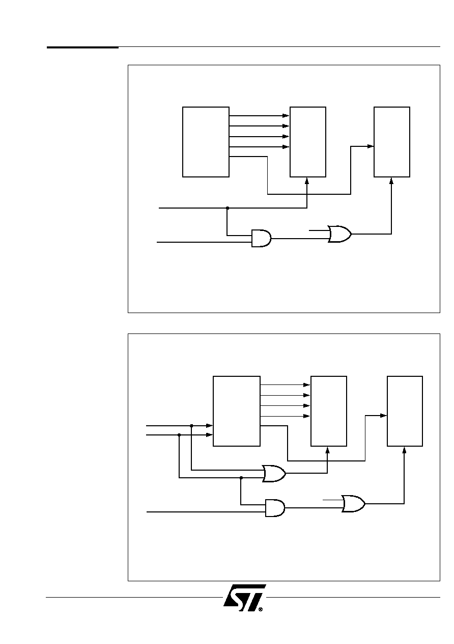
PSD5XX Family
55
Figure 27a. 8031 Memory Modes
EPROM
DPLD
SRAM
ES0
ES1
ES2
ES3
RS0
RD
OE
OE
SRCODE≠EN
PSEN
SEPARATE SPACE MODE
Memory
Block
(Cont.)
Figure 27b. 8031 Memory Modes
EPROM
DPLD
SRAM
ES0
ES1
ES2
ES3
RS0
PSEN
RD
RD
OE
OE
SRCODE≠EN
PSEN
RD
COMBINED SPACE MODE

PSD5XX Family
56
9.4.5 Peripheral I/O
The Peripheral I/O Mode is one of the operating modes of Port A. In this mode, Port A
is connected to the data bus of peripheral devices. Port A is enabled only when the
microcontroller is accessing the devices, otherwise the Port is tri-stated. This feature
enables the microcontroller to access external devices without requiring buffers and
decoders. Figure 28 shows the structure of Port A in the Peripheral I/O Mode.
The memory address space occupied by the devices are defined by two signals: PSEL0
and PSEL1. The signals are direct outputs from the DPLD. Whenever any of the signals is
active, the Port A driver is enabled, and the direction of the data flow is determined by the
RD/WR signals.
The Peripheral I/O Mode and the peripheral select signals are configured and defined in the
PSDsoft Software (see the section on I/O Port for configurations). The PIO bit in the VM
Register (see Table 16) also needs to be set to "1" by the user to initialize the Peripheral I/O
Mode.
The Peripheral I/O mode can be used, for example, in DMA applications where the
microcontroller does not support DMA operations, such as tri-stating the address/data bus.
Figure 29 shows a block diagram of a microcontroller and PSD5XX based design that
makes use of this mode. In this application, the microcontroller has a multiplexed bus which
is connected to the ADIO port. The C and D ports connect to the peripheral address bus
and are both configured in Address Out Mode. Port A is configured in the Peripheral I/O
mode and is connected to the peripheral data bus. Port B and E are used to generate
control signals.
During normal activity, the microcontroller has access to any peripheral (memory or I/O
device) through the PSD5XX device. When there is a DMA request, the microcontroller
tri-states the address bus on Port C and D by writing a "0" to the port Direction Registers.
The DMA controller then takes over the data and address buses after receiving
acknowledgement from the microcontroller.
Figure 28. Port A In Peripheral I/O Mode
RD
PSEL0
PSEL1
D0 ≠ D7
WR
PA0 ≠ PA7
Peripheral I/O
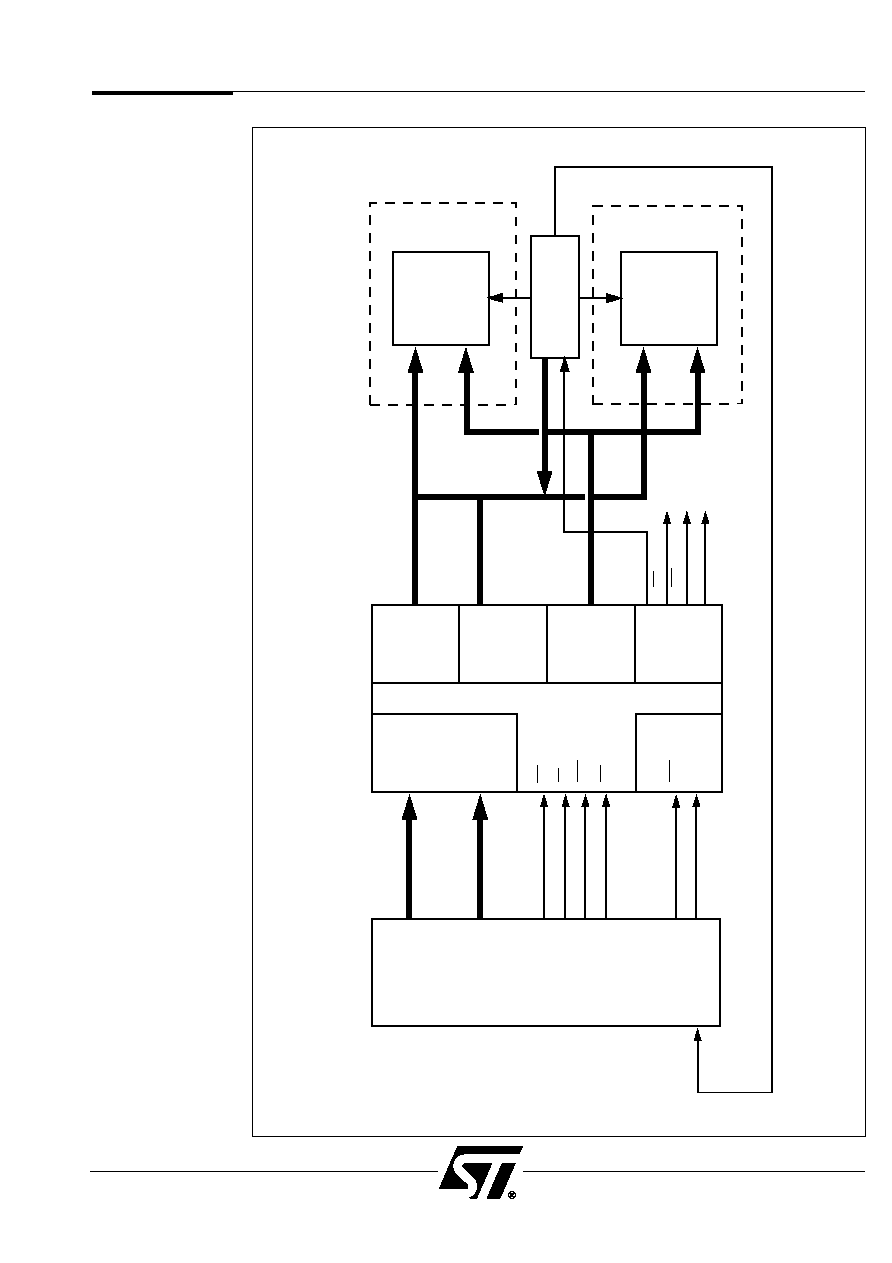
PSD5XX Family
57
Figure 29. PSD5XX Peripheral I/O Configuration
MICRO-
CONTROLLER
AD
[ 0 ≠ 7
]
A
[ 8 ≠15
]
A
[ 0 ≠ 7
]
A
[ 8 ≠ 15
]
D
[ 0 ≠ 7
]
DMA ACK
ADIO
PORT
PORT E
WR
RD
RST
CSI
BHE
ALE
PORT C
PORT D
PORT A
PORT B
PSD5XX
MEMORY
I/O
DEVICE
DMA
CONTROLLER
PERIPHERAL # 1
PERIPHERAL # 2
DMA
≠
REQ
RD
WR
CSi
Peripheral I/O

PSD5XX Family
58
The PSD5XX provides many power saving options. By configuring the PMMRs (Power
Management Mode Registers), the user can reduce power consumption. Table 17 shows
the bit configuration of the PMMR0 and PMMR1. The microcontroller is able to control the
power consumption by changing the PMMR bits at run time.
9.5.1 Standby Mode
There are two Standby Modes in the PSD5XX:
t
Power Down Mode
t
Sleep Mode
9.5.2 Power Down
In this mode, the internal devices are shut down except for the I/O ports. There are three
ways the PSD5XX can enter into the Power Down Mode: by controlling the CSI input,
by activating the Automatic Power Down (APD) Logic, or when none of the inputs are
changing and the turbo bit is off.
t
The CSI
The CSI input pin is an active low signal. When low, the signal selects and enables the
PSD5XX. The PSD5XX enters into Power Down Mode immediately when the signal
turns high. This signal can be controlled by the microcontroller, external logic or it can
be grounded.
The CSI turns off the internal bus buffers in standby mode. The address and control
signals from the microcontroller are blocked from entering the ZPLD as inputs.
t
The APD Logic
The APD unit enables the user to enter a power down mode independent of controlling
the CSI input. This feature eliminates the need for external logic (decoders and latches)
to power down the PSD. The APD unit concept is based on tracking the activity on the
ALE pin. If the APD unit is enabled and ALE is not active, the 4-bit APD counter starts
counting and will overflow after 15 clocks, generating a PD (Power Down) signal
powering down the PSD. If sleep mode is enabled, then PD signal will also activate the
sleep mode. Immediately after ALE starts pulsing the PSD will get out of the power
down or sleep mode.
The operation of APD is controlled by the PMMR (see Figure 30a). PMMR1 bit 0 selects
the source of the APD counter clock. After reset the APD counter clock is connected to
PE7 (APD_CLK) on the PSD. In order to guarantee that the APD will not overflow there
should be less than 15 APD clocks between two ALE pulses. If CLKIN frequency is
adequate, then it can be connected to the APD and PE7 is used for other functions.
The next step is to select the ALE power down polarity. Usually, MCUs entering power
down will freeze their ALE at logic high or low. By programming bit 1 of PMMR0 the
power down polarity can be defined for the APD. If the APD detects that the ALE is
in the power down polarity for 15 APD counter clocks then the PSD will enter a power
down mode. To enable the APD operation, bit 2 in the PMMR0 should be set high.
9.5.3 Sleep Mode
The Sleep Mode is activated if the SLEEP EN bit, the APD EN bit, and the ALE Polarity bit
in the PMMR are set, and the APD Counter has overflowed after 15 clocks (see Figure 30).
In Sleep Mode the PSD5XX consumes less power than the Power Down Mode, with typical
I
CC
reduced to 10 µA (1 µA for ZPSD5XX devices).
In this mode, the Counter/Timers, the Interrupt Controller and the ZPLD still monitor their
inputs and respond to them. As soon as the ALE starts pulsing, the PSD5XX exits the
Sleep Mode.
The PSD access time from Sleep Mode is specified by t
LVDV1
. The ZPLD response time to
an input transition is specified by t
LVDV2
.
9.5
Power
Management
Unit
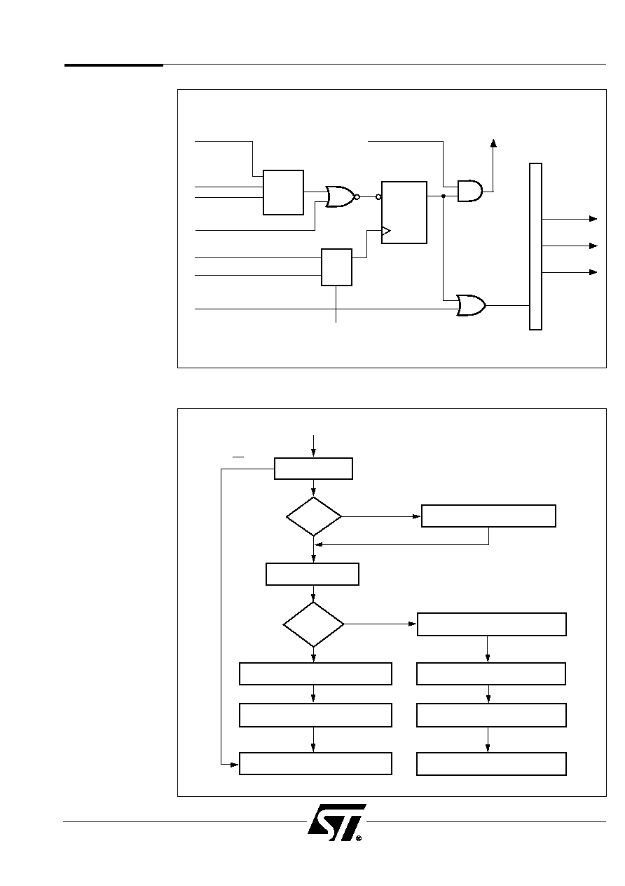
PSD5XX Family
59
CLR
CLK
APD
COUNTER
APD CLK
PMMR1 - BIT 0
TO OTHER
CIRCUITS
MUX
APD
CLEAR
LOGIC
APD ENABLE
PMMR0 - BIT 2
ALE POLARITY
PMMR0 - BIT 1
ALE
RESET
APD CLK
CLKIN
CSI
SLEEP ≠ ENABLE
PMMR1 - BIT 1
SLEEP
MODE
EPROM
SELECT
SRAM
SELECT
I/O
SELECT
POWER
DOWN
PD
Z
P
L
D
Figure 30. Power Management Unit
Figure 30a. Automatic Power Down Unit (APD) Flow Chart
APD DISABLED
NEED
APD CLK
YES
YES
NO
NO
RESET
SET APD CLK IN PMMR1 BIT 0
SET ALE PD POLARITY
IN PMMRO BIT 1
CSI = "1"
NEED
SLEEP
MODE
SET SLEEP MODE IN PMMR1 BIT 1
ALE IDLE and
15 APD CLOCK
ALE IDLE and
15 APD CLOCK
∑ SET ENABLE APD IN PMMR0 BIT 2
∑ SET PMMR0 BIT 0
∑ SET ENABLE APD IN PMMR0 BIT 2
∑ SET PMMR0 BIT 0
DISABLE CLOCKS
ZPLD ACLK, ZPLD RCLK, TMR ZPLD
DISABLE CLOCKS
ZPLD ACLK, ZPLD RCLK, TMR ZPLD
PSD IN POWER DOWN MODE
PSD IN SLEEP MODE
Power
Management
Unit
(Cont.)
PSD5XX Family
60
APD EN Bit
ALE Power
ALE Status
APD Counter
Down Polarity
0
X
X
Not Counting
1
X
Pulsing
Not Counting
1
1
1
Counting (Activates Standby
Mode After 15 Clocks)
1
0
0
Counting (Activates Standby
Mode After 15 Clocks)
Bit 7
Bit 6
Bit 5
Bit 4
Bit 3
Bit 2
Bit 1
Bit 0
TMR CLK
ZPLD
ZPLD
ZPLD
APD
ALE PD
*
RCLK
ACLK
TURBO
CMISER
ENABLE
Polarity
1 = OFF
1 = OFF
1 = OFF
1 = OFF
1 = ON
1 = ON
1 = HIGH
PMMR0
Bit 7
Bit 6
Bit 5
Bit 4
Bit 3
Bit 2
Bit 1
Bit 0
*
*
*
*
*
*
Sleep
APD CLK
Mode
1 = ON
1 = CLKIN
PMMR1
Table 17. Power Management Mode Registers (PMMR0, PMMR1)
Table 18. APD Counter Operation
Power
Management
Unit
(Cont.)
Bit 0
*
= Should be set to High (1) to operate the APD.
Bit 1 0 = ALE Power Down (PD) Polarity Low.
1 = ALE Power Down (PD) Polarity High.
Bit 2 0 = Automatic Power Down (APD) Disable.
1 = Automatic Power Down (APD) Enable.
Bit 3 0 = EPROM/SRAM CMiser is OFF.
1 = EPROM/SRAM CMiser is ON.
Bit 4 0 = ZPLD Turbo is ON. ZPLD is always ON.
1 = ZPLD Turbo is OFF. ZPLD will Power Down when inputs are not changing.
Bit 5 0 = ZPLD Clock Input into the Array from the CLKIN pin input is connected. Every
Clock change will Power Up the ZPLD when Turbo bit is OFF.
1 = ZPLD Clock Input into the Array from the CLKIN pin input is disconnected.
Bit 6 0 = ZPLD Clock Input into the the MacroCell registers from the CLKIN pin input
is connected.
1 = ZPLD Clock Input into the the MacroCell registers from the CLKIN pin input
is disconnected.
Bit 7 0 = In the PSD5XX Clock Input is connected to the Timer.
1 = In the PSD5XX Clock Input is disconnected from the Timer.
Bit 0
0 = Automatic Power Down Unit Clock is connected to Port E7 (PE7) alternate
function input.
1 = Automatic Power Down Unit Clock is connected to the PSD Clock
input (CLKIN).
Bit 1
0 = Sleep Mode Disabled.
1 = Sleep Mode Enabled.
Bit 2≠7 0 = Reserved for future use, should be set to zero.

PSD5XX Family
61
Power
Management
Unit
(Cont.)
9.5.4 Other Power Saving Options
The PSD5XX provides additional power saving options. These options, except the SRAM
Standby Mode, can be enabled/disabled by setting up the corresponding bit in the PMMR.
t EPROM
The EPROM power consumption in the PSD is controlled by bit 3 in the
PMMR0 ≠ EPROM CMiser. Upon reset the CMiser bit is OFF. This will cause the
EPROM to be ON at all times as long as CSI is enabled (low). The reason this mode is
provided is to reduce the access time of the EPROM by 10 ns relative to the low power
condition when CMiser is ON. If CSI is disabled (high) the EPROM will be deselected
and will enter standby mode (OFF) overriding the state of the CMiser.
If CMiser is set (ON) then the EPROM will enter the standby mode when not selected.
This condition can take place when CSI is high or when CSI is low and the EPROM is
not accessed. For example, if the MCU is accessing the SRAM, the EPROM will be
deselected and will be in low power mode.
An additional advantage of the CMiser is achieved when the PSD is configured in the
by 8 mode (8 bit data bus). In this case an additional power savings is achieved in the
EPROM (and also in the SRAM) by turning off 1/2 of the array even when the EPROM
is accessed (the array is divided internally into odd and even arrays).
The power consumption for the different EPROM modes is given in the DC
Characteristics table under I
CC
(DC) EPROM Adder.
t SRAM Standby Mode
The SRAM has a dedicated supply voltage V
STBY
that can be used to connect a
battery. When V
CC
becomes lower than V
STBY
≠0.6 then the PSD will automatically
connect the V
STBY
as a power source to the SRAM. The SRAM Standby Current (I
STBY
)
is typically 0.5 µA.
SRAM data retention voltage V
DF
is 2 V minimum.
t Zero Power ZPLD
ZPLD power/speed is controlled by the ZPLD_Turbo bit (bit 4) in the PMMR0. After
reset the ZPLD is in Turbo mode and runs at full power and speed. By setting the bit to
"1", the Turbo mode is disabled and the ZPLD is consuming Zero Power current if the
inputs are not switching for an extended time of 100 ns. The propagation delay time will
be increased by 10ns after the Turbo bitis set to "1" (turned off) if the inputs change at a
frequency of less than 15 MHz.
PSD5XX Family
62
Power
Management
Unit
(Cont.)
Port Configuration
Pin Status
I/O Port
Unchanged
ZPLD Output
Depend on Inputs to the ZPLD
Address Out
Undefined
Data Port
Tri-stated
Special Function Out
Depending on Status of Clock Input
Peripheral I/O
Tri-stated
Table 20. I/O Pin Status During Power Down And Sleep Mode
t Input Clock
The PSD5XX provides the option to turn off the clock inputs to save AC power
consumption. The clock input (CLKIN) is used as a source for driving the following
modules:
t
ZPLD Array Clock Input
t
ZPLD MacroCell Clock Flip Flop
t
APD Counter Clock
t
Counter/Timers Clock
During power down or if any of the modules are not being used the clock to these
modules should be disabled. To reduce AC power consumption, it is especially important
to disable the clock input to the ZPLDS array if it is not used as part of a logic equation.
The ZPLD Array Clock can be disabled by setting PMMR0 bit 5 (ZPLD ACLK). The ZPLD
MacroCell Clock Input can be disabled by setting PMMR0 bit 6 (ZPLD RCLK). The Timer
Clock can be disabled by setting PMMR0 bit 7 (TMR CLK). The APD Counter Clock
will be disabled automatically if Power Down or Sleep Mode is entered through the APD
unit. The input buffer of the CLKIN input will be disabled if bits 5 ≠ 7 PMMR0 are set and
the APD has overflowed.
The Counter/Timers can operate in Sleep Mode if the TMR CLK bit is low, but the power
consumption will be based on the frequency of operation (CLKIN frequency).
NOTES: 1. Power Down does not affect the operation of the ZPLD. The ZPLD operation in this mode is based
only on the ZPLD_Turbo Bit.
2. In Sleep Mode any input to the ZPLD will have a propagation delay of t
LVDV2
.
3. PLD recovery time to normal operation after exiting Sleep Mode. An input to the ZPLD during the
transition will have a propagation delay time of t
LVDV3
.
PLD
PLD
Access
Access
Propagation
Recovery
Time
Recovery
Delay
Time To
Time To
Normal
Normal
Operation
Access
Power Down
Normal t
PD
0
No Access
t
LVDV
(Note 1)
Sleep
t
LVDV2
t
LVDV3
No Access
t
LVDV1
(Note 2)
(Note 3)
Summary of PSD5XX Timing and Standby Current During Power Down
and Sleep Modes

PSD5XX Family
63
General Description
The PSD5XX contains a powerful set of four 16 bit Counter/Timers, each controlled by
either PPLD outputs, external pins or Software. The Counter/Timers aid the user in
counting external events and/or generating accurate delays. These can be operated
as Counters or Timers. In Event-count, time capture and WatchDog modes, the
Counter/Timers work as Counters, whereas in Waveform and Pulse modes they work as
Timers. All Counter/Timers are capable of generating interrupts through the On-Board
Interrupt Controller. Each of the Counter/Timers consist of a Counter/Timer Command
register, Counter/Timer Image register and Counter/Timer register. All four Counter/Timers
share a Global command register, a Software Load/Store register, a Freeze command
register and the Status register. Counter/Timer 2 can support WatchDog operations.
All Counter/Timers share a common clock input and Delay Cycle register used in scaling
down the input clock to the Counter/Timer. The maximum resolution of the Counter/Timer
is the input clock of the PSD5XX divided by four. The maximum input clock frequency to
the PSD5XX is 30 MHz. Figures 31 and 32 describe the general features of the
Counter/Timers.
Features
t
Four 16 bit Counter/Timers.
t
Five modes of operation
≠ Waveform Mode
≠ Pulse Mode
≠ Event Counter Mode
≠ Time Capture Mode
≠ WatchDog Mode
*
t
Each Counter/Timer can be controlled by an input pin, dedicated PPLD macrocell or
software.
t
Each Counter/Timer has an output to the Interrupt Controller.
t
The WatchDog output is routed through the PLD and can be programmed to be
output at any PLD output pin.
t
Programmable input and output polarity.
t
Counter/Timer can be programmed as UP or DOWN Counter, except in
WatchDog mode.
t
All Counters have the operating frequency range of DC to 7.0 MHz
(i.e 143 ns maximum resolution at 7.0 MHz). Higher resolution can be achieved
by using in conjunction with the GPLD macrocells.
t
High resolution Divisor unit for Counter clocking purposes.
t
Can easily interface with any 8 or 16 bit Microcontroller or Microprocessor.
See Process Change Notice related to Event Count Mode on page 148.
9.6
PSD5XX
Counter/Timer
(
*
) Counter/Timer-2 can operate in WatchDog mode.
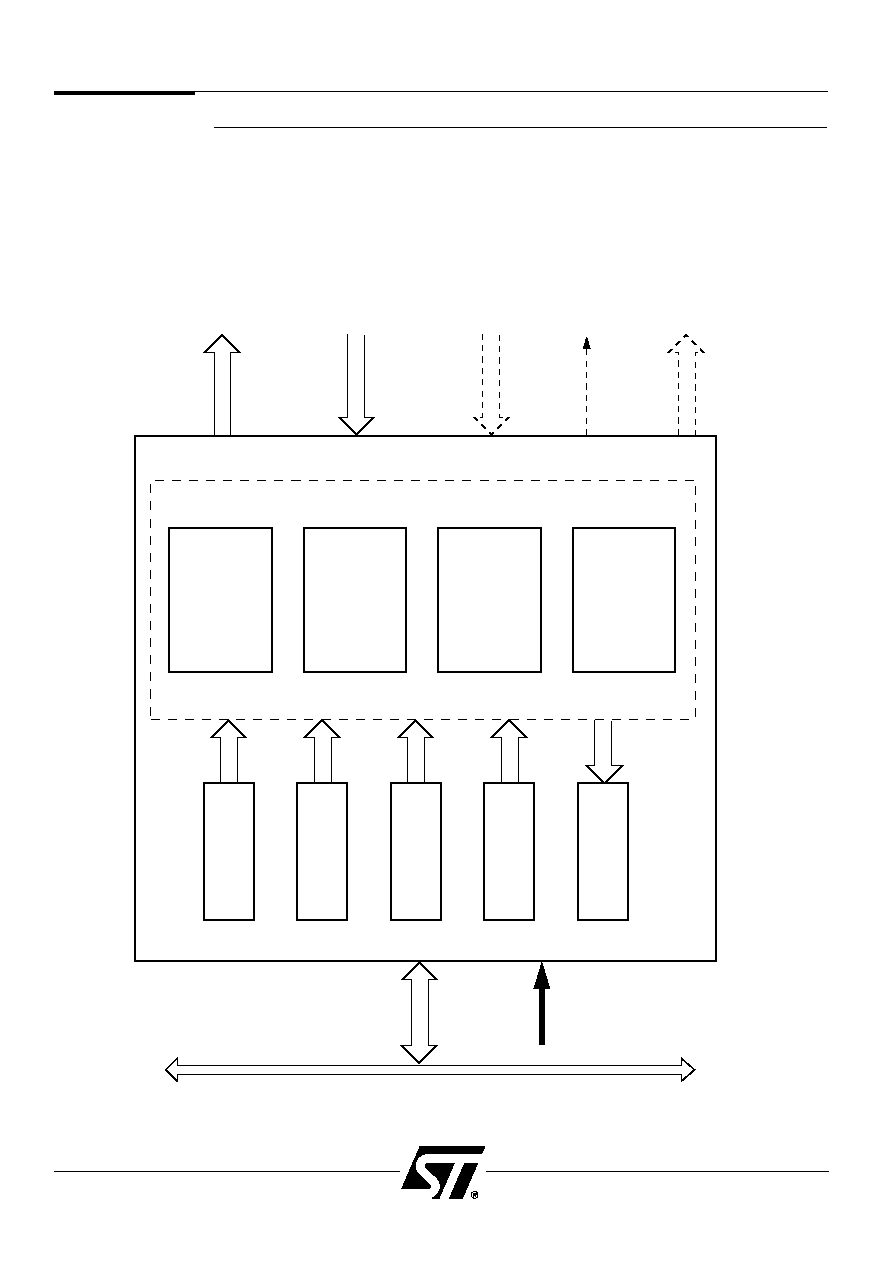
PSD5XX Family
64
Figure 31. Counter/Timer Block Diagram
GLOBAL
COMMAND
REGISTER
DELAY CYCLE
REGISTER
FREEZE
COMMAND
REGISTER
SOFTWARE
LOAD
/
STORE
REGISTER
STATUS
REGISTER
CONTROL
TIMER
/
COUNTER 0
TIMER
/
COUNTER 1
TIMER
/
COUNTER 2
*
TIMER /
COUNTER 3
CTU0
CTU1
CTU2
CTU3
*
Can also function as WatchDog timer
PA0 ≠ PA3
OR
PB0 ≠ PB3
PSD5XX
DATA BUS
TERMINAL COUNTS
TO INTERRUPT
CONTROLLER AND
PORT E
PE3 ≠ PE6
PPLD
MACROCELLS
WATCHDOG
OUTPUT TO PPLD
TIMER /COUNTER
OUTPUTS
PIN CONTROL
PSD5XX
Counter/Timer
(Cont.)
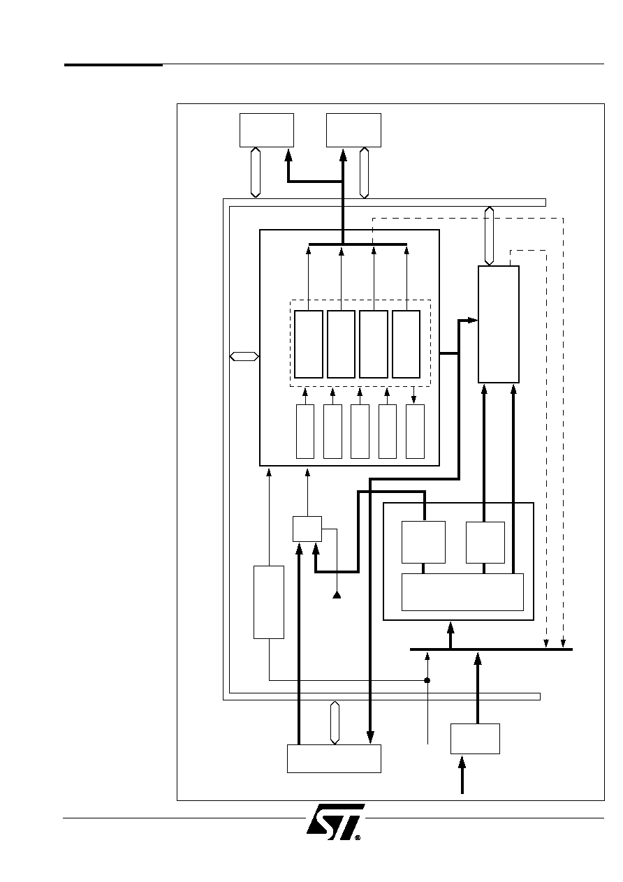
PSD5XX Family
65
Figure 32.
Counter/Timer and Interrupt Controller Interface with Other Internal Blocks
PORT
E
PIN/
MACROCELL
COMMAND
INPUT
PROGRAMMABLE
CLOCK
PRESCALER
GLOBAL CMD REG
DLCY REG
FREEZE CMD REG
S'WARE
LOAD/STORE
STATUS
REG
COUNTER
/
TIMER 0
COUNTER
/
TIMER 1
COUNTER/
TIMER 2
COUNTER/
TIMER 3
CTU0
CTU1
CTU2
CTU3
TIMER
OUTPUTS
PA0 ≠ PA3
TIMER
OUTPUTS
PB0 ≠ PB3
PORT
A
PORT
B
TIMER0
≠
OUT
TIMER1
≠
OUT
TIMER2
≠
OUT
TIMER3
≠
OUT
TIMER
[ 3 : 0
] ≠
IN
MC2INT
[ 6 : 7
]
TC0
≠
TC3
TC0
≠
TC3
MC2TMR
[ 3 : 0
]
PT2INT
[ 4 : 5
]
CONTROL
BUS
INTRF
CLKIN
ZPLD
INPUT
BUS
AND
ARRAY
TIMER
MACRO-
CELL
INTR
MACRO-
CELL
INTERRUPT
CONTROLLER
ADDRESS
/
DATA
/
CONTROL BUS
COUNTER
/
TIMER
UNIT
MUX
PPLD
WDOG2PLD
INTR2PLD
TIMER CLOCK
CLOCK IN
PE4
≠
PE7
PSD5XX
Counter/Timer
(Cont.)

PSD5XX Family
66
Counter Name
Counting Register
Image Register
Counter 0
CNTR0
IMG0
Counter 1
CNTR1
IMG1
Counter 2
CNTR2
IMG2
Counter 3
CNTR3
IMG3
9.6.1 Counter/Timer Operation
There are four identical 16 bit Counter/Timers CNTR0,CNTR1,CNTR2 and CNTR3 and
associated Counter/Timer image registers IMG0,IMG1,IMG2 and IMG3. Refer to Table 21
for counter name and register correspondence. All Counter/Timers share a common clock
source. Each Counter/Timer can be operated in either WAVEFORM / PULSE mode or
EVENT COUNTER/TIME CAPTURE mode. Counter 2 can be set up as a Watchdog timer in
both modes. Note that in Event Counter/Time Capture mode COUNTER 2 can only be set
up as a Watch Dog Counter/Timer, whereas in the Waveform/Pulse mode Counter 2 can be
configured as a Pulse or Waveform generator or as a Watchdog timer. Refer to Table 24 for
possible combinations of Counter/Timer modes and refer to Figure 33 for additional details.
Each Counter/Timer can be controlled by an input pin or through a dedicated PPLD
macrocell output or by software. Counter/Timer outputs are available through port A or
port B pins in alternate function mode (Refer to the chapter on I/O ports). Polarity of
these inputs/outputs is software programmable. The following sections describe various
command and data registers that need to be initialized for proper function of these
Counter/Timers.
9.6.1.1 Counter/Timer Operating Modes
The PSD5XX Counter/Timer has five basic modes of operation: The Waveform and Pulse
or Event Counter, Time Capture, and Watchdog. The Waveform and Pulse modes cannot
be used in conjunction with Event and Time Capture modes. Both Waveform/Pulse or
Event Count/Time Capture modes can set Counter 2 into the fifth mode of operation, the
"WatchDog" mode.
The basic functional element used in all these modes is the Counter/Timer unit (CTU)
illustrated in Figure 33. This block consists of a 16 bit increment/decrement Counter, and a
16 bit image register with various control signals. The key function of the image register is
to enable microcontroller access of the Counter without asynchronously interrupting the
Counter. Software can configure each Counter/Timer using the associated Command
register. The Counter/Timer of the PSD5XX employs four CTUs to realize the various
modes of operation.
Table 21. Registers Used By Counters
PSD5XX
Counter/Timer
Operation
(Cont.)
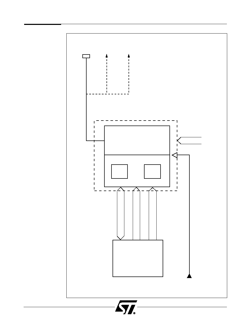
PSD5XX Family
67
Figure 33. Inside of Each CTUx (x = 0, 1, 2, 3)
MICRO
-
CONTROLLER
DATA
ADDRESS
SOFTWARE
COMMANDS
IMAGE
REG
CMD
REG
COUNTER
CTU
x
TIMER CLOCK
PPLD MACROCELL
OR PIN OR
SOFTWARE
COMMAND INPUT
TERMINAL COUNT (TC)
TO INTERRUPT
CONTROLLER
TERMINAL COUNT (TC)
TO PORT E
COUNTER
OUTPUT AT PINS
PA
x OR PB
x
*
x = 0 TO 7
*
Not applicable in Event Count or Time Capture modes.
PSD5XX
Counter/Timer
Operation
(Cont.)

PSD5XX Family
68
9.6.1.2 Waveform Mode
In Waveform mode, the Counter/Timer is capable of producing various pulse-width
modulated (PWM) signals. The Waveform mode in the PSD5XX is realized using two CTUs
(COUNTER/TIMER UNITs) in the following combinations:
CTU0 & CTU1 or CTU2 & CTU3.
The outputs of CTU0 and CTU2 are available at Port A and Port B. Refer to Tables 25 and
26 for further details and configuration of these ports. CTU1 and CTU3 are internally
connected to CTU0 and CTU2. The Waveform mode is illustrated in Figure 34 which shows
a typical PWM waveform and the time slots in which two CTUs are active. The Waveform
period is the sum of the counts for CTU0 and CTU1 (see equation 1), while the duty cycle is
given by equation 2. The Duty cycle of a waveform can be changed by loading a new value
into the corresponding IMAGE register, and as soon as a Terminal Count is generated this
new value gets loaded into the CTU. Note that the end of a CTU time slot is indicated with
Terminal Count signal of the active CTU. The Terminal Count signals are used to signal the
transfer of active status between CTUs. The Terminal Count is true whenever the Counter
underflows while decrementing or when the Counter overflows while incrementing.
PERIOD of the waveform generated
= COUNT HIGH + COUNT LOW..(1)
DUTY Cycle of the Waveform Generated
=
COUNT HIGH
COUNT HIGH + COUNT LOW......(2)
The timing of various pulses that create a Waveform signal in the above example is defined
by the Microcontroller via image register updates of the CTU0 and CTU1. The contents of
an image register are loaded or copied to the associated Counter under any of the following
conditions:
t
Terminal Count of CTU1 and/or CTU3 pulses to transfer active status to CTU0
and/or CTU2.
t
An input pin (port E) pulses (If enabled by software).
t
A PPLD macrocell output pulses (If enabled by software).
t
A command register bit is written to by the Microcontroller, i.e., a software
Load/Store (load).
A Waveform output is first initialized and then later modified by setting its two corresponding
software Load/Store bits after loading of the Image Registers. If the Counter/Timer register
is directly loaded by the MCU, it gets overwritten by the associated Image register contents
as soon as the Counter/Timer is active. The configuration of the CTU in the waveform mode
is schematically illustrated in Figure 35.
The output polarity during the CTU0 time slot is controlled by bit 3 in the Counter/Timer
command register. The output polarity during the CTU1 time slot is defined as the
complement of the CTU0 polarity. Similarly, the polarity of the input pin is controlled by bit 4
in the Counter/Timer command register. This description of the waveform mode of operation
applies to CTU2 and CTU3 also.
In order to change the image register values, use the Freeze/Freeze Acknowledge protocol
as described in the Freeze Command Register section.
Counter/Timer
Operation
(Cont.)

PSD5XX Family
69
Figure 34. Sample Waveform (PWM) and CTU Time Slots
(Using Counters/Timers 0 and 1)
OUTPUT
WAVEFORM
*
TERMINAL
COUNT 0
TERMINAL
COUNT 1
CTU0 ACTIVE
*
Output Waveform is available at pin PA0 or PB0 depending on the PSDsoft fitter pin assignment.
CTU1 ACTIVE
CTU1 ACTIVE
CTU0 ACTIVE
CTU0 ACTIVE
Counter/Timer
Operation
(Cont.)

PSD5XX Family
70
Figure 35. CTU Control Signals For Waveform Mode
COUNTER
START COUNTER (BIT 1 OF GLOBAL COMMAND REGISTER)
COUNTER OUTPUT (PORT A OR B)
(ONLY COUNTER 0 OR 2)
OUTPUT POLARITY SELECT (BIT 3 OF CMD REGISTER)
SOFTWARE FREEZE (FREEZE COMMAND REGISTER)
TIMER_CLOCK
*
Need two CTUs together in Waveform Mode (CTU0 ≠ CTU1 or CTU2 ≠ CTU3).
The Terminal Count of CTU0 drives CTU1 and the Terminal Count of CTU1 drives CTU0.
The same applies to CTU2 and CTU3.
SOFTWARE SELECT (BIT 2 OF CMD REGISTER)
SOFTWARE ENABLE (BIT 7 OF CMD REGISTER)
TERMINAL COUNT OF OTHER CTU
*
PIN OR MACROCELL
(SELECTED BY BIT 5 OF CMD REGISTER)
SOFTWARE GATE BIT
(BIT 6 OF CMD REGISTER)
INCREMENT/DECREMENT SELECT (BIT 1 OF CMD REGISTER)
SOFTWARE LOAD (SOFTWARE LOAD / STORE REGISTER)
TERMINAL COUNT (TC)
TO INTERRUPT CONTROLLER
FREEZE ACKNOWLEDGE
(STATUS FLAGS REGISTER)
TERMINAL COUNT (TC)
*
TO OTHER CTU
LOAD / STORE
ENABLE/DISABLE
TERMINAL COUNT (TC)
TO PORT E
Counter/Timer
Operation
(Cont.)

PSD5XX Family
71
9.6.1.3 Pulse Mode
In Pulse mode, the Counter/Timer is capable of generating a one shot pulse. The Pulse
width of the generated pulse is defined by the value loaded into the associated Image
register of the timer. If the Counter/Timer register is directly loaded by the MCU, it gets
overwritten by the associated Image register contents as soon as the Counter/Timer
is active. Each CTU is capable of pulse mode. As soon as the Timer is active,
i.e. decrementing or incrementing, a pulse is output until the Timer underflows or overflows.
The pulse waveform is illustrated in Figure 36. The active level of this pulse is defined
again by a command register bit. As can be seen in Figure 37, the pulse is triggered by any
of the following events:
t
Transition on the input pin (Port E) (If enabled by software).
t
PPLD macrocell output pulses (If enabled by software).
t
Command register bit is written to by a Microcontroller (Software load).
As in the waveform mode, the polarity of the input pin is defined by a command register
bit and the Freeze/Freeze Acknowledge must be used whenever the image register is
modified.
The outputs of CTU0, CTU1, CTU2 and CTU3 are available at Port A and Port B. Refer to
Tables 25 and 26 for further details and configuration of these ports.
9.6.1.4 Event Counter Mode
In this mode, the Counter/Timer uses the CTU to count a number of events. An event is
defined as a signal-transition on the Counter's input pin as defined by the input polarity
configuration bit in the Command Registers or a Low to High transition on the PPLD
Macrocell output. In this mode, the image register of the CTU is used to store the contents
of the Counter at the rising edge of the Load/Store signal. This is opposed to the previous
two modes in which the image register was used to load the Counter. Figure 38 shows the
configuration of the CTU for the event-Counter mode. Notice that the enable signal is edge
sensitive. Its source is either:
t
Pin Driven.
t
PPLD Macrocell Driven.
All Counter/Timer registers must be assigned values during initialization in the Event
Counter mode. During normal operation, the CTU increments or decrements its count
when an event occurs. The image register is then immediately updated with the current
count. The microcontroller can read the contents of the image register by first setting the
command-register Freeze bit in order to disable count updates of the image register during
its read operation. The microcontroller waits for a freeze acknowledge and then accesses
the image register in the usual fashion. The Freeze signal effectively guarantees stable
image register data during microcontroller read access, even though the CTU continues to
count events. During the Freeze Acknowledge active state, the counter continues counting.
Note that for an event to be counted the events must be separated by at least one timer
clock period plus two CLKIN clock periods.
Counter/Timer
Operation
(Cont.)
PSD5XX Family
72
Figure 36. Sample Pulse-Mode Waveform
OUTPUT
WAVEFORM
TERMINAL
COUNT
PULSE
TRIGGER
EVENT
CTU INACTIVE
CTU INACTIVE
CTU ACTIVED BY A
LOAD/STORE PULSE
Counter/Timer
Operation
(Cont.)
PSD5XX Family
73
Figure 37. CTU Control Signals For Pulse Mode
COUNTER
START COUNTER (BIT 1 OF GLOBAL COMMAND REGISTER)
COUNTER OUTPUT (PORT A OR B)
OUTPUT POLARITY SELECT (BIT 3 OF CMD REGISTER)
SOFTWARE FREEZE ( FREEZE COMMAND REGISTER)
TIMER_CLOCK
SOFTWARE SELECT BIT (BIT 2 OF CMD REGISTER)
ENABLE COMMAND (BIT 7 OF CMD REGISTER)
PIN OR MACROCELL
(SELECTED BY BIT 5 OF CMD REGISTER)
SOFTWARE GATING BIT
(BIT 6 OF CMD REGISTER)
INCREMENT/DECREMENT SELECT (BIT 1 OF CMD REGISTER)
SOFTWARE LOAD (SOFTWARE LOAD
/ STORE REGISTER)
TERMINAL COUNT (TC)
TO INTERRUPT CONTROLLER
FREEZE ACKNOWLEDGE
(STATUS FLAGS REGISTER)
LOAD
/
STORE
ENABLE/DISABLE
TERMINAL COUNT (TC)
TO PORT E
Counter/Timer
Operation
(Cont.)
PSD5XX Family
74
Figure 38. CTU Control Signals For Event Count Mode
COUNTER
START COUNTER (BIT 1 OF GLOBAL COMMAND REGISTER)
TIMER_CLOCK
SOFTWARE SELECT (BIT 2 OF CMD REGISTER)
ENABLE COMMAND
(BIT 7 OF CMD REGISTER)
PIN OR MACROCELL (BIT 5 OF CMD REGISTER)
PIN OR MACROCELL
(SELECTED BY BIT 5 OF CMD REGISTER)
SOFTWARE GATING BIT
(BIT 6 OF CMD REGISTER)
SOFTWARE FREEZE (FREEZE COMMAND REGISTER)
*
SOFTWARE STORE (SOFTWARE LOAD
/ STORE REGISTER)
TERMINAL COUNT (TC)
TO INTERRUPT CONTROLLER
FREEZE ACKNOWLEDGE
(STATUS FLAGS REGISTER)
LOAD
/
STORE
ENABLE/DISABLE
*
Count updates are continuously stored in the image register, unless frozen by the software freeze command.
TERMINAL COUNT (TC)
TO PORT E
Counter/Timer
Operation
(Cont.)

PSD5XX Family
75
9.6.1.5 Time Capture Mode
In the time capture mode, the Counter/Timer is capable of measuring the time
(by counting clock pulses) between events. Figure 39 shows the CTU configuration for
time capture. All the Counter/Timer registers must be cleared during initialization of the
Time Capture mode. Here the Counter is enabled to count via software only. The CTUs
continuously count. A Load/Store pulse triggers the storing of the Counter's contents into
the associated image register. The image register effectively contains a "snap shot" of the
Counter at the time of the pulse. The CTU Store input is edge-triggered by events, the
events being:
t
Pin Driven.
t
PPLD Macrocell Driven.
t
Software Driven.
A Freeze signal is used to ensure that image data is stable during Microcontroller reads
which is similar to the description of event Counter Microcontroller read accesses. Two
CTUs in time capture mode can be used to capture the rising and the falling edges of a
pulse, the difference of the measurements being the pulse width. The counter continues to
count regardless of the Freeze Acknowledge state.
Note that the time span between two consecutive edges of Time Capture must be greater
than one timer clock cycle in order to be captured.
9.6.1.6 WatchDog Counter/Timer
Counter/Timer-2 can be operated as a WatchDog Timer in both Waveform/Pulse and Event
count/time capture modes. In Event count/time capture mode, Counter/Timer-2 can be
configured only as WatchDog. Figure 40 shows the control signals of the CTU when in
WatchDog mode. When the WatchDog mode is active, CTU2 counts down and at the
terminal count of Counter-2 a WatchDog condition occurs. To avoid the WatchDog from
occurring, a "Write" to the Software Load/Store Bit-2 in the "Software Load/Store Register"
has to take place before the Counter-2 underflows. This action reloads the Counter-2 with
the initial count value in the Image Register-2. Note that this initial count value cannot be
changed after the WatchDog mode is enabled.
The Terminal Count signal of a WatchDog could result in a pulse width that is equal to the
count value loaded into the Image Register of Counter/Timer-2. The active high WatchDog
pulse from Counter 2 is routed through the PPLD, enabling the user to inverse its polarity or
implement any other logic before driving the WatchDog output on a user defined I/O pin.
This signal could be used to drive a RESET pin or trigger a Non-Maskable interrupt on a
processor. Once Counter/Timer-2 is set to the WatchDog mode, it cannot be reconfigured
by software and it can get out of the WatchDog mode only by a RESET.
When the WatchDog is enabled in Power Down and Sleep modes, it remains active
regardless of the state of bit 7 (TMR CLK) in Power Management Mode Register PMMR0.
The WatchDog mode is enabled by setting the WatchDog bit in the global command
register. Setting up the command register for CTU2 is not required except when CTU3 is
configured in pulse mode. In this case, bit 0 of the command register for CTU2 is set to "1".
Counter/Timer
Operation
(Cont.)

PSD5XX Family
76
Counter/Timer
Operation
(Cont.)
Figure 39. CTU Control Signals For Time Capture Mode
COUNTER
START COUNTER (BIT 1 OF GLOBAL COMMAND REGISTER)
TIMER_CLOCK
SOFTWARE SELECT (BIT 2 OF CMD REGISTER)
PIN OR MACROCELL
(SELECTED BY BIT 5 OF CMD REGISTER)
SOFTWARE GATE BIT
(BIT 6 OF CMD REGISTER)
SOFTWARE FREEZE (FREEZE COMMAND REGISTER)
SOFTWARE STORE (SOFTWARE LOAD
/
STORE REGISTER)
TERMINAL COUNT (TC)
TO INTERRUPT CONTROLLER
FREEZE ACKNOWLEDGE
(STATUS FLAGS REGISTER)
STORE
ENABLE/DISABLE
TERMINAL COUNT (TC)
TO PORT E
PSD5XX Family
77
Figure 40. CTU Control Signals For WatchDog Mode
SET WATCHDOG BIT
(BIT 3 OF GLOBAL COMMAND REGISTER)
C
O
U
N
T
E
R
2
I
M
A
G
E
2
GPLD
SOFTWARE LOAD
(BIT 2 OF SOFTWARE LOAD / STORE REGISTER)
OUTPUT
PIN
WDOG2PLD
COUNTER OUTPUT
(ACTIVE HIGH)
WATCHDOG
GPLD
OUTPUT
TERMINAL COUNT TO
INTERRUPT CONTROLLER
TERMINAL COUNT TO
PORT E
TIMER_CLOCK
EN / DIS
LOAD
(SELF LATCHING BIT)
Counter
/
Timer
Operation
(Cont.)
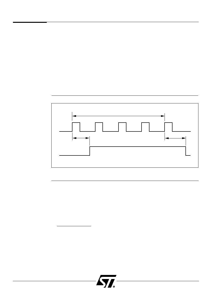
PSD5XX Family
78
Counter/Timer
Operation
(Cont.)
9.6.1.8 Counter/Timer Clock Input
All Counter/Timers 0 through 3 have a common clock source. The Counter/Timers are
clocked from the output of a highly flexible and high resolution Divisor unit. The Divisor's
input is the external Clock input pin. The Divisor DIV is a number in the range of
4
<
= DIV
<
= 280. Refer to Table 22 for exact values of DIV for different clock values.
Figure 42 details the PSD5XX Counter clock generation.
The Counter/Timer CLOCK input
=
(External Clock input)
(DIV)
where DIV = N
*
K and N = (4 + DLCY).
The value of K depends on the Scale-Bit (Bit 0 in the Global Command Register) in the
"Global Command Register" , K = 8 when Scale-Bit is set to 1 and K = 1 when Scale-Bit is
set to 0. DLCY is the number of Delay Cycles in the range of 0
<
= DLCY
<
= 31 set up in the
Delay Cycle Register. The fastest clock to service the Counter/Timer is = (Clock input / 4).
The maximum External Clock input value is 28 MHz and the fastest internal count frequency
is 7.0 MHz, i.e., a resolution of 143 ns. (Higher resolution can be achieved by using in
conjunction with GPLD macrocells). The default value of DIV is 4 (following a reset both K
and DLCY contain zeroes).
9.6.1.7 Terminal Counts (TCs)
The terminal counts (TC0 ≠ TC3) generated by the Counter/Timers are made available
at Port E as outputs or as feedbacks to the ZPLD. Refer to Table 27a for pin assignments.
The terminal counts can be used to concatenate the 16-bit Counter/Timers into a
larger counter. Only the trailing edge of the TC signal can be used as input to another
Counter/Timer. For example, concatenating CTU0 and CTU1 requires the following
PPLD equation in the PSDabel file:
mc2t mr1 = tc0;
In order for a TC signal to come out, its respective bit in the Port E Special Function Out
Register must be set to 1. TC signals on Port E pins can be used as inputs to the ZPLD.
A TC signal goes high for the duration of at least four CLKIN periods whenever its
corresponding Timer Counting-Register overflows or underflows.
Figure 41 gives the timing relationship between CLKIN and the TC signal.
Figure 41. Timing Relationship Between CLKIN and the TC Signal.
4 CLKIN PERIODS
CLKIN
TC - SIGNAL
30ns
30ns
NOTES: 1. Overflow occurs when a counter value changes from FFFFh to 0000h during incrementing.
2. Underflow occurs when a counter value changes from 0000h to FFFFh during decrementing.
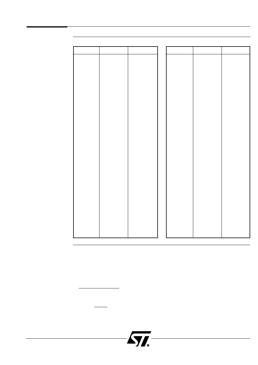
PSD5XX Family
79
DLCY
Scale Bit
DIV
0
0
4
1
0
5
2
0
6
3
0
7
4
0
8
5
0
9
6
0
10
7
0
11
8
0
12
9
0
13
10
0
14
11
0
15
12
0
16
13
0
17
14
0
18
15
0
19
16
0
20
17
0
21
18
0
22
19
0
23
20
0
24
21
0
25
22
0
26
23
0
27
24
0
28
25
0
29
26
0
30
27
0
31
28
0
32
29
0
33
30
0
34
31
0
35
DLCY
Scale Bit
DIV
1
1
40
2
1
48
3
1
56
4
1
64
5
1
72
6
1
80
7
1
88
8
1
96
9
1
104
10
1
112
11
1
120
12
1
128
13
1
136
14
1
144
15
1
152
16
1
160
17
1
168
18
1
176
19
1
184
20
1
192
21
1
200
22
1
208
23
1
216
24
1
224
25
1
232
26
1
240
27
1
248
28
1
256
29
1
264
30
1
272
31
1
280
Table 22. DLCY, Scale Bit and DIV to Generate Different Clock Divisions
Sample Calculation of Timer Input Clock
External input clock to the PSD5XX is 8 MHz.
If required Counter/Timers 0 ≠ 3 count frequency is 1 MHz then
The Counter/Timer CLOCK Input
=
(External Clock input)
(DIV)
8 MHz
1 MHz =
=
>
(DIV) = 8
(DIV)
Therefore from Table 22 when (DIV) = 8, the Scale-Bit in the "Global Command Register" is
set to a 0 and the DLCY register to a value of 4.
Counter/Timer
Operation
(Cont.)
Counter/Timer Clock Input
(Cont.)
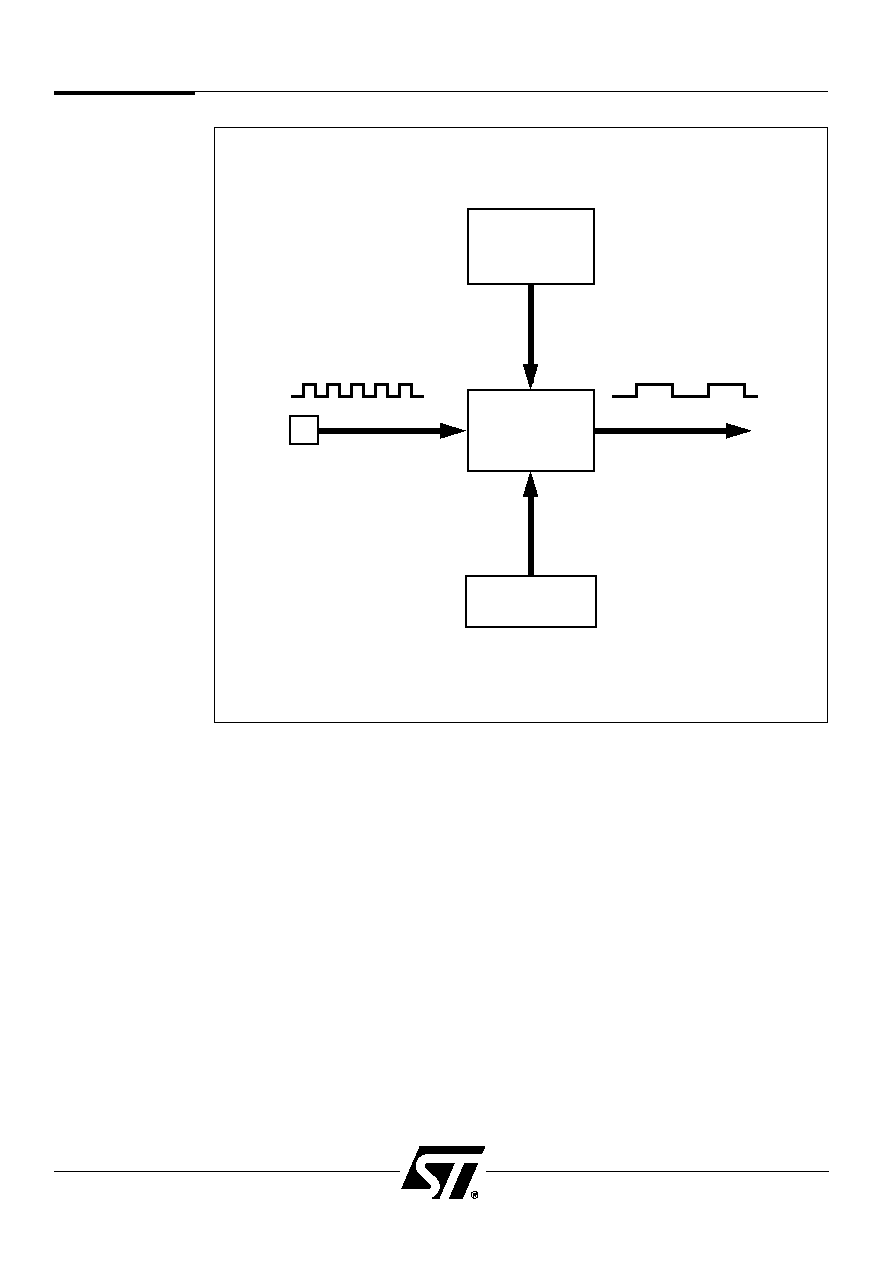
PSD5XX Family
80
Counter/Timer
Operation
(Cont.)
Figure 42. Counter Clock Generation
RESULTING
DIVISOR VALUE
4
<
= DIV
<
= 280
SCALE BIT
IN GLOBAL CMD
REGISTER
DELAY CYCLE
REGISTER
0
<
= DLCY
<
= 31
TIMER CLOCK TO
COUNTERS / TIMERS 0 ≠ 3
CLKIN
PIN
PSD5XX Family
81
Address
Register Name
Address
Register Name
Offset
Offset
+A9h
STATUS FLAGS
+A8h
GLOBAL COMMAND
+A6h
DLCY
+A5h
SOFTWARE LOAD/STORE
+A4h
FREEZE COMMAND
+A3h
CMD3
+A2h
CMD2
+A1h
CMD1
+A0h
CMD0
+9Fh
CNTR3
+9Eh
CNTR3
+9Dh
CNTR2
+9Ch
CNTR2
+9Bh
CNTR1
+9Ah
CNTR1
+99h
CNTR0
+98h
CNTR0
+97h
IMG3
+96h
IMG3
+95h
IMG2
+94h
IMG2
+93h
IMG1
+92h
IMG1
+91h
IMG0
+90h
IMG0
Table 23. Offset Address Map of Counter/Timer-Unit Registers
Counter/Timer
Operation
(Cont.)
9.6.2 Counter/Timer Registers
Registers CNTR0,CNTR1,CNTR2 and CNTR3 serve as actual counting logic. Registers
IMG0,IMG1,IMG2 and IMG3 serve as images of these Counter/Timers. Depending upon the
selected mode of operation, a Counter can load a new value or transfer its content to the
image register. Registers IMG0 - IMG3 and CNTR0 - CNTR3 are accessible to the
Microcontroller only before setting the start bit (Bit 1 in the Global Command Register).
When CNTR0-CNTR3 are active, the value in the read operation is not guaranteed to be
stable and during a write operation there could be contention between the image register
write and microcontroller write. Therefore the access of registers CNTR0-CNTR3 should
be suspended when the Counter/Timers are active. Only IMG0, IMG1, IMG2 and IMG3
registers are accessible when the Counter/Timers are active.
Tables 23 and 23a give the address map for the various port and Counter/Timer-unit
registers. This address offset map is of the host processor, relative to CSIOP (Chip Select
Input Output Port) i.e. address space allocated by the host Microcontroller to access all the
PSD5XX embedded peripherals.
Table 23a is for 16-bit Motorola Microcontrollers which require different address offsets.
PSD5XX Family
82
Address
Register Name
Address
Register Name
Offset
Offset
+A8h
STATUS FLAGS
+A9h
GLOBAL COMMAND
+A7h
DLCY
+A4h
SOFTWARE LOAD/STORE
+A5h
FREEZE COMMAND
+A2h
CMD3
+A3h
CMD2
+A0h
CMD1
+A1h
CMD0
+9Eh
CNTR3
+9Fh
CNTR3
+9Ch
CNTR2
+9Dh
CNTR2
+9Ah
CNTR1
+9Bh
CNTR1
+98h
CNTR0
+99h
CNTR0
+96h
IMG3
+97h
IMG3
+94h
IMG2
+95h
IMG2
+92h
IMG1
+93h
IMG1
+90h
IMG0
+91h
IMG0
Table 23a. Offset Address Map of Counter/Timer-Unit Registers
(For 16-Bit Motorola MCUs in 16-Bit Mode. If 8-Bit Mode is selected, use Table 23.)
Registers IMG0 through IMG3 are written to by the microcontroller to load the
Counter/Timers with required values in Waveform, Pulse and WatchDog mode only.
To retrieve the count or time in Event count or Time capture modes, Counter/Timers store
their values into IMG0 through IMG3.
Any access to the Image Registers must conform to the Freeze/Freeze Acknowledge
protocol, described later in the Freeze Command paragraph.
Counter/Timer
Registers
(Cont.)

PSD5XX Family
83
9.6.2.1 Global Command Register
This is used to specify the operation mode of the Counter/Timer and to start or stop the
Counter/Timer. Therefore during the initialization of the Counter/Timer registers, the Global
Command Register should always be configured last.
Counter/Timer
Registers
(Cont.)
Bit 7
Bit 6
Bit 5
Bit 4
Bit 3
Bit 2
Bit 1
Bit 0
*
*
*
*
Watch
Global
Counter
Scale
Dog
Mode
Start
NOTE:
*
= Not used.
At RESET all bits come up as 0's.
Watch Dog Bit:
When this bit is
0: Watch Dog mode is NOT selected.
1: Watch Dog Counter/Timer (Counter 2) is active. This bit can be
turned off by RESET only.
NOTE: Whenever this bit is set to 1, the COUNTER START bit should
also be set to 1. Otherwise the Counter/Timer will always be off,
i.e., once this bit is set, access to Counter 2 Registers and the Global
Command Registers are blocked.
Global Mode Bit:
When this bit is set to a
0: All Timers/Counters are set to Waveform or Pulse Mode.
1: All Timers/Counters are set to operate in Event Counter or Time
Capture Mode.
NOTE: Further selection of modes is done in individual CMD registers.
Counter Start Bit: When this bit is set to
0: ALL CTUs are disabled and can be re-initialized.
1: ALL CTUs are enabled.
Scale Bit:
When this bit is set to
0: The clock to all Counter/Timers is divided by 1.
1: The clock to all Counter/Timers is divided by 8.
PSD5XX Family
84
9.6.2.2 Command Registers for Counter/Timers CMD0, CMD1, CMD2, CMD3:
Each of the Counter/Timer units (CTU) has one Command Register associated with it.
A description of these various CTU command bits is provided below. Refer to CSIOP
Tables 23 and 24 for their addresses and selection details. Figure 43 describes the
Command Register bits.
The following is the description of Counter/Timer0 CMD0 register bits. Bits in CMD1, CMD2
and CMD3 have similar descriptions. Refer to Figure 43 also.
Counter/Timer
Registers
(Cont.)
Bit 7
Bit 6
Bit 5
Bit 4
Bit 3
Bit 2
Bit 1
Bit 0
Enable/
Software
Pin /
Input
Output
Select
Increment /
Mode
Disable
Gating
PPLD
Polarity
Polarity
Counter
Decrement
Select
Using
Bit for
Macrocell
Pin,
Load /
PPLD
Store cmd
Macrocell
Using Pin
or or
PPLD
Software
Macrocell
NOTES: 1. At RESET these bits come up as 0s.
2. In WatchDog Mode, CMD2 register bits are Don't Cares.
Mode Select Bit (0):
This bit selects the Counter/Timer0 operation mode. After
RESET Counter/Timer0 initializes in waveform/event count
mode. When this bit is set to
1: The Counter/Timer0 operates in Pulse/Time capture
modes.
0: The Counter/Timer0 operates in Waveform/Event count
modes.
NOTE: See Table 24 for details of Timer mode set up.
Increment/Decrement Bit (1): This bit is used to set the Counter/Timer in increment or
decrement mode. The RESET state is Decrement mode.
When this bit is set to
1: The Counter/Timer0 is in increment mode.
0: The Counter/Timer0 is in decrement mode.
NOTE: In WatchDog mode Counter #2 is in decrement
mode only.
Select Counter Bit (2):
This bit is used to select or deselect Counter/Timer0.
At RESET this bit initializes as 0 which means
Counter/Timer0 is deselected. When this bit is set to
1: Counter/Timer0 is selected (counting enabled).
0: Counter/Timer0 is deselected (counting disabled).
After a Counter/Timer is started by the Global Command Register, it can be re-configured by
changing the individual Command Register. The steps to re-configure a Counter/Timer are:
1. Disable the Counter/Timer by writing a "0" to the Select Counter Bit (bit 2) of the
Command Register.
2. Change the Counter/Timer configuration by writing the new value (bit 2 remains at "0")
to the Command Register.
3. Enable the Counter/Timer again by writing the new value with bit 2 set to "1" to the
Command Register.

PSD5XX Family
85
Command Registers for Counter/Timers CMD0, CMD1, CMD2, CMD3 (Cont.)
Output Polarity Bit (3):
This bit is valid only in Waveform or Pulse mode and is
used to select the polarity of the Active output signal
of the Counter/Timer0. At RESET this bit initializes as 0
which means the Active output state is LOW. When this bit
is set to a
1: The Active output state is HIGH.
0: The Active output state is LOW.
Input Polarity Bit (4):
The state of this bit determines the polarity of the Active
input control signal to the Counter/Timer0 and is valid only
for input pin. At RESET this bit initializes as 0 which means
that the input Active is HIGH. When this bit is set to a
1: The input Active is LOW.
0: The input Active is HIGH.
Pin / PPLD Macrocell Bit (5): This bit determines whether the Counter/Timer0 gets its
input command for Load/Store and Enable/Disable from
the PSD5XX PIN or from the PPLD macrocell output.
At RESET this bit initializes as 0 which means that the
input command is coming from the PSD5XX PPLD
macrocell. When this bit is set to a
1: The Counter/Timer0 input command is coming from
the PIN.
0: The Counter/Timer0 input command is coming
from the PPLD macrocell output.
Software Gating Bit for
This bit gates the Load/Store command activated by the
Load/Store Commands (6):
PSD5XX PIN or PPLD macrocell. At RESET this bit
initializes as 0 which means that the Load/Store command
activated by the PIN or macrocell is permitted through.
When this bit is set to
1: Load/Store operation activated by PIN or Macrocell is
NOT permitted through.
0: Load/Store operation activated by PIN or macrocell is
permitted through. To further decide between the PIN
and PPLD macrocell, use bit 5 (PIN/PPLD macrocell).
Enable/Disable Using PIN,
This bit determines whether the Enable/Disable
PPLD Macrocell or Software command is activated by the PSD5XX Pin, PPLD macrocell
Bit (7):
or by Software. At RESET this bit initializes as 0, which
means that the Enable/Disable command is activated by
the PIN or PPLD macrocell. When this bit is set to
1: Enable/Disable command by PIN or macrocell is
overridden by Software (only Bit 2 of this register will
enable or disable the counter).
0: Enable/Disable command is activated by PIN or
Macrocell output. To further decide between the PIN and
PPLD macrocell use bit 5 (PIN / PPLD macrocell bit).
Counter/Timer
Registers
(Cont.)

PSD5XX Family
86
FROM COUNTER PPLD MACROCELL OUTPUT
MC2TMR
[ 3 : 0
]
COUNTER CONTROL INPUT PIN
TIMER
[ 3 : 0
]
≠
IN
Input Polarity
Bit 4 of CMD0 Register
Software Select
Counter Bit 2
of CMD0 Register
Software
Load/Store
BIT0 of Software
Load
/Store
Register
Freeze Command
Bit0 of
Freeze Command Register
Pin or Macrocell
Select Bit 5
of CMD0 Register
Software Gating Bit
for Load
/
Store
Commands from
Pin or Macrocell
Bit 6 of CMD0 Register
Enable
/
Disable
Using Pin, Macrocell
or Software
Bit 7 of CMD0 Register
MUX
ENABLE / DISABLE
SIGNAL TO TIMER
LEVEL
SENSITIVE
LOAD / STORE
SIGNAL TO TIMER
RISING EDGE
SENSITIVE
Figure 43. Enable/Disable and Load/Store Generation
Counter/Timer
Registers
(Cont.)
PSD5XX Family
87
9.6.2.3 Configuring the Mode of Operation of the Counter/Timers:
Using the GLOBAL MODE bit of the Global Command register and MODE SELECT bit of
the Command register of Counter/Timers 0 ≠ 3, individual Counter/Timer modes of operation
can be set up. Refer to Table 24. Notice that all the Counter/Timers can either operate in
Waveform/Pulse or Event Count/Time Capture modes, but not in all four modes at the same
time.
Counter/Timer
Registers
(Cont.)
Mode Select Bit
Global Mode Bit
(Command Modes
Modes
(Global Command
Registers of
of
of
Register)
Counter/Timers
Counter/Timers
Counter/Timer2
0 ≠ 3 CMD0, CMD1,
0, 1 and 3
CMD2 and CMD3)
0
0
Waveform
Waveform or
WatchDog
0
1
Pulse
Pulse or
WatchDog
1
0
Event Counter
WatchDog Only
1
1
Time Capture
WatchDog Only
9.6.2.4 Freeze Command Register
When a Microcontroller needs to access the contents of the Image Registers (IMG0-IMG3)
it does so by first setting the Command Register Freeze bit in order to disable the timer
state-machine accesses of the Image Register. The Microcontroller waits for the Freeze
Acknowledge bit in the Counter/Timer Status Register to be set to 1 and then it accesses
the Image Register as an address location. The freeze acknowledge signal effectively guar-
antees stable Image Register data during Microcontroller read/write cycles even though the
Counter/Timer continues to count. The Freeze Acknowledge bit gets cleared after the
negation of Freeze. The Freeze Command bits are set and cleared by the microcontroller
software.
The Freeze Command Register and the software Load/Store Register should not be set at
the same time. It is recommended that the registers be accessed individually.
Bit 7
Bit 6
Bit 5
Bit 4
Bit 3
Bit 2
Bit 1
Bit 0
*
*
*
*
Freeze
Freeze
Freeze
Freeze
CTU3
CTU2
CTU1
CTU0
NOTE:
*
= Not used.
Table 24. Counter/Timer Modes

PSD5XX Family
88
9.6.2.5 Software Load/Store Register:
Each bit in this register enables a load to the corresponding Counter/Timer from its
associated Image Register in Waveform, Pulse or WatchDog modes. The actual counts
are stored in their corresponding Image Register in event Counter or time capture modes.
Bit 6 of the Command Register must be set to "1" before writing to the software load/store
register.
Counter/Timer
Registers
(Cont.)
Software Load/Store 0 Bit: If this bit is set to
1: Counter/Timer0 CNTR0 gets loaded from the Image
Register IMG0 or CNTR0 stores into IMG0 based on the
mode of operation
**
.
Software Load/Store 1 Bit: If this bit is set to
1: Counter/Timer1 CNTR1 gets loaded from the Image
Register IMG1 or CNTR1 stores into IMG1 based on the
mode of operation
**
.
Software Load/Store 2 Bit: If this bit is set to
1: Counter/Timer2 CNTR2 gets loaded from the Image
Register IMG2.
Software Load/Store 3 Bit: If this bit is set to
1: Counter/Timer3 CNTR3 gets loaded from the Image
Register IMG3 or CNTR3 stores into IMG3 based on the
mode of operation
**
.
**
Load operation takes place in Waveform, Pulse and WatchDog mode.
Store operation takes place in Event Count and Time Capture mode.
Bit 7
Bit 6
Bit 5
Bit 4
Bit 3
Bit 2
Bit 1
Bit 0
*
*
*
*
Software
Software
Software
Software
Load/Store 3 Load/Store 2 Load/Store 1 Load/Store 0
NOTE:
*
= Not used.
The Software load/store bits are automatically cleared by the served Counter.
In addition to four CTU registers, there are delay cycle and Counter/Timer status registers.
These are summarized on the following pages.

PSD5XX Family
89
Bit 7
Bit 6
Bit 5
Bit 4
Bit 3
Bit 2
Bit 1
Bit 0
*
*
*
*
FrezAck3
FrezAck2
FrezAck1
FrezAck0
NOTES: At RESET all these bits intialize as 0's.
*
= Not used.
9.6.2.6 Status Flags Register
There are eight READ-ONLY status flags. The lower four bits represent Freeze
Acknowledge bits.
Counter/Timer
Registers
(Cont.)
FrezAck Bits
These Freeze Acknowledge bits are useful in the Freeze/Freeze Acknowledge protocol.
After the Microcontroller senses that the FrezAck bit is being set it proceeds to access the
Image Register for a read or write operation.
FrezAck0 Bit:
When this bit is
1:
Image Register Access is granted.
0:
Image Register Access is not granted.
FrezAck1 Bit:
When this bit is
1:
Image Register Access is granted.
0:
Image Register Access is not granted.
FrezAck2 Bit:
When this bit is
1:
Image Register Access is granted.
0:
Image Register Access is not granted.
FrezAck3 Bit:
When this bit is
1:
Image Register Access is granted.
0:
Image Register Access is not granted.
DLCY Register:
Bits
<
4:0
>
of the DLCY register are used to assign Delay Cycles to the Counter/Timer.
Various Clock Scaling values possible are 0 through 31 (decimal).
At RESET these bits initialize as 0. If necessary, the user has the option to set these bits up
to generate Delay Cycles (DLCY) to scale down the Counter/Timer clock (see Table 24).
Bit 7
Bit 6
Bit 5
Bit 4
Bit 3
Bit 2
Bit 1
Bit 0
*
*
*
DLCY4
DLCY3
DLCY2
DLCY1
DLCY0
NOTE:
*
= Not used.

PSD5XX Family
90
9.6.2.7 Load/Store
The Load operation transacts an Image Register (e.g. IMG0) write into its Counter/Timer
Register (e.g. CNTR0), whereas in the Store operation the Counter/Timer Register (e.g.
CNTR0) writes back into the Image Register (e.g. IMG0).
These signals are valid only when a Counter/timer is active. They are rising edge sensitive
and are used to Load a Counter with a required value or to Store the Counter value in the
associated Image Register.
In Waveform, Pulse and WatchDog modes the microcontroller writes into an Image
Register. The respective Counter/Timer uses that value as its initial counting value. The
data transfer operation from an Image Register into its corresponding counter is called
LOAD. In Event Counting and Time Capture modes the Counter/Timer counts event pulses
or timer clock cycles, respectively. An external event or a software command can cause a
data transfer from the counting element into its Image Register. This operation is defined as
STORE.
These operations are triggered by:
t
Software command
t
Terminal count (in Waveform mode only)
t
PPLD macrocell output
t
Input Pin
Refer to Counter/Timer Command Register and Figure 43 for specific details.
9.6.2.8 Enable/Disable
These signals are used to enable or disable the counting of the Counter/Timers. These
signals are controlled by:
t
Software command (Bits 2 and 7 of the Command Registers).
t
PPLD macrocell output
t
Input Pin
Event Count Mode:
In Event Count mode the Enable/Disable signal is edge sensitive and is connected to the
event input signal through the PPLD or pin. In Time Capture mode the Enable/Disable
signal can be set by a software command only.
Refer to Counter/Timer Command Register and Figure 43 for specific details.
9.6.2.9 Counter/Timer Input/Output
Each Counter can use individual control inputs in port E as input Load/Store or
Enable/Disable signals, and Counter/Timer outputs in port A or port B by selecting alternate
and special functions on the pins assigned to them. The outputs are used in waveform and
pulse modes in which the Counters generate output waveforms or pulses. The inputs can
be used in all modes of operation except WatchDog to create the LOAD/STORE and/or
ENABLE/DISABLE control signals. Port E can be configured as outputs for Terminal Count.
Terminal Count is also available as ZPLD inputs (via pin feedback). Refer to Tables 25, 26
and 27 for further details and configuration of these ports.
9.6.2.10 PPLD Macrocell
The enable/disable or load/store inputs of each Counter/Timer can be selected through a
PPLD macrocell, whose inputs are two product terms PTT0 and PTT1 from the PPLD's
AND-array. The polarity of the PPLD macrocell output is programmable. The output of the
PPLD macrocell which is the enable/disable and/or Load/Store input to the Counter/Timer
can be in a Combinatorial mode or Register mode. Figure 44 shows the details of the PPLD
macrocell. Refer to the "ZPLD" section for further information on the PPLD.
Counter/Timer
(Cont.)
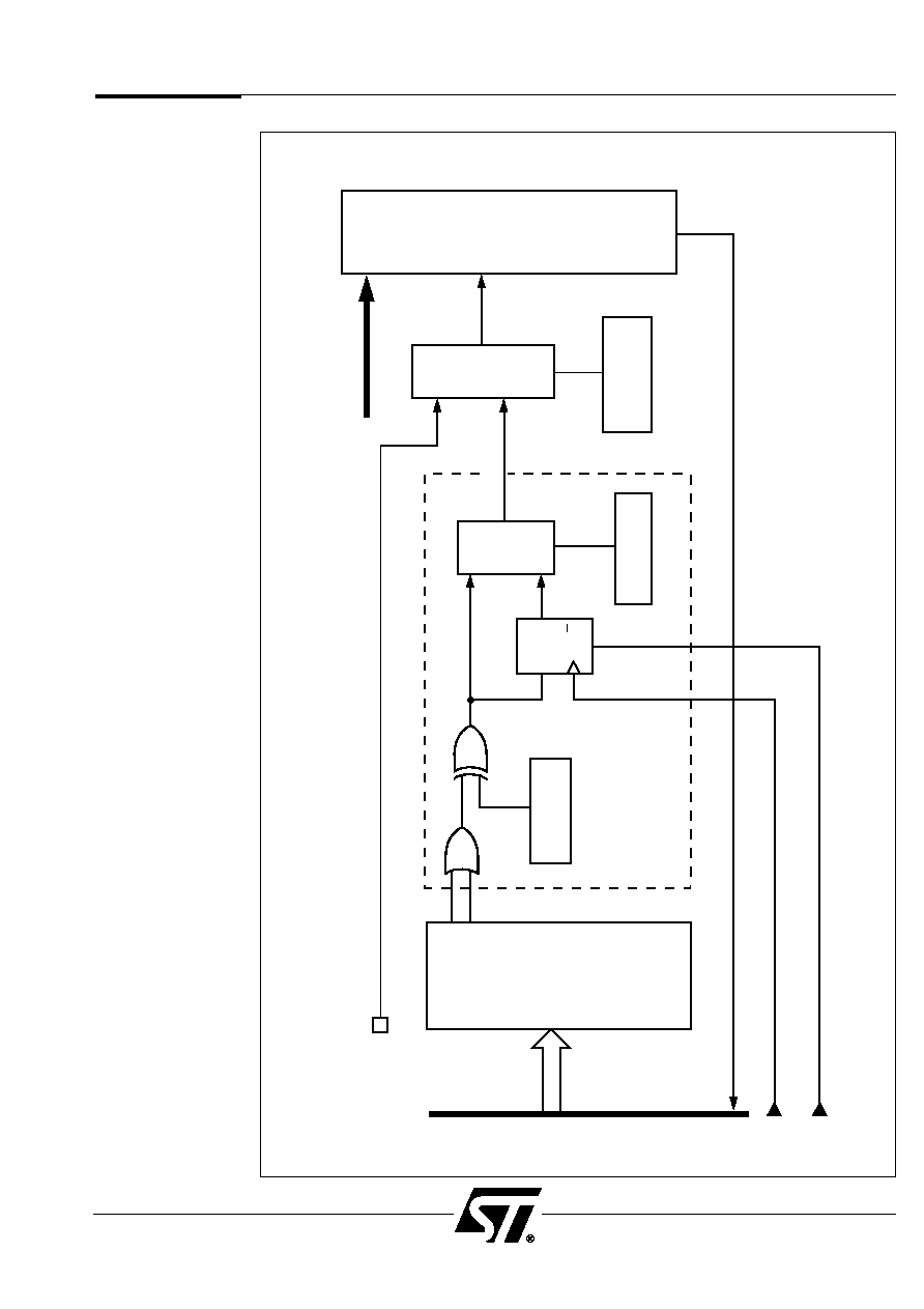
PSD5XX Family
91
Figure 44. PPLD Macrocell For Each Counter/Timer
AND
ARRAY
TIMER
[ 3 : 0
] ≠
IN
CLKIN
RESET
WDOG2PLD (INTERNAL FEEDBACK)
POLARITY
SELECT
COUNTER
/
TIMER
BIT 5 OF
COMMAND REGISTER
ZPLD
INPUT
BUS
PIN OR
MACROCELL
SELECT
INPUT
MUX
COMB / REG
SELECT
MUX
PR
DQ
Q
C
TIMER
_CLOCK
(PRESCALED CLK)
MC2TMR
*
TIMER
INPUT PIN
PT
T≠
0
PT
T≠1
*
*
These are four similar Macrocells with outputs MC2TMR
[
3:0
]
.abl FILE
Counter/Timer
(Cont.)

PSD5XX Family
92
Counter/Timer
(Cont.)
9.6.2.11 I/O ≠ Port A, B, E
Ports A, B and E have the capabilities for counter/timer alternate and special functions,
e.g. Counter/Timer out, load/store, enable/disable, etc. Refer also to the chapter on I/O
ports for further details.
Table 25.
Port Pin
Special Function Out
PA0
Timer0_out
PA1
Timer1_out
PA2
Timer2_out
PA3
Timer3_out
Port Pin
Special Function Out
PB0
Timer0_out
PB1
Timer1_out (in Pulse Mode Only)
PB2
Timer2_out
PB3
Timer3_out (in Pulse Mode Only)
Special Function Assignment
Port A:
Timer outputs in Pulse or Waveform modes can be tapped out of these pins: PA0 ≠ PA3.
In order for the following timer outputs to drive their corresponding port pins, set the
respective bits in the Special Function Register of Port A to ones.
Table 26.
Port B:
Timer outputs in Pulse or Waveform modes can be tapped out of these pins: PB0 ≠ PB3.
In order for the following timer outputs to drive their corresponding port pins, set the
respective bits in the Special Function Register of Port B to ones.
The decision which of Port A or B pins are used as timer outputs is done by the
PSDsoft fitter.

PSD5XX Family
93
Port Pin
Alternate Function In
PE3
Timer0_in
PE4
Timer1_in
PE5
Timer2_in
PE6
Timer3_in
I/O ≠ Port A, B, E
(Cont.)
Port E:
Timer[3:0] _ inputs can have different control functions such as timer LOAD/STORE and/or
ENABLE/DISABLE, based on how these pins are configured in the Timer Command
Registers.
Table 27.
Counter/Timer
(Cont.)
Port Pin
Special Function Out
PE4
TC0
PE5
TC1
PE6
TC2
PE7
TC3
Table 27a.
The Terminal Counts (TC0 ≠ TC3) generated by each Counter/Timer are available at Port E
(pins PE4 ≠ PE7) as shown in Table 27a.
To Connect TC0 ≠ TC3 to Port E pins, set the corresponding bits in the Special Function
Register to "1".

PSD5XX Family
94
Counter/Timer
(Cont.)
9.6.2.12 Sample Counter/Timer0 Initialization In PULSE Mode
Following is a sample initialization routine for Counter/Timer0 to operate in PULSE mode.
The assembly language commands do not correspond to any particular microcontroller.
Configure CSIOP for Microcontroller access to Counter/Timer registers and I/O ports for
initialization of Counter/Timers. For the values of each register, refer to Tables 30 and 31.
Use PSDsoft supplied by WSI to configure the portion related to Counter/Timers. Also refer
to the Section on the PSD5XX I/O Ports.
Clear All Counter/Timers
LOAD CNTR0, 0000h
; Clear Counter/Timer 0
LOAD CNTR1, 0000h
; Clear Counter/Timer 1
LOAD CNTR2, 0000h
; Clear Counter/Timer 2
LOAD CNTR3, 0000h
; Clear Counter/Timer 3
Scaling of Clock (common to all Counter/Timers)
LOAD DLCY, 02h
;Delay Cycles(DLCY) = 2, k value is selected in
;Global Register by setting Scale-Bit
Counter/Timer 0 Initialization (Command Register0 CMD0)
LOAD CMD0, 6Fh
;Pulse mode (D0 = 1)
;Increment (D1 = 1)
;Select Counter/Timer (D2 = 1)
;Output Pulse Active High (D3 = 1)
;Load Signal on Input pin High going transition (D4 = 0)
;Input control from PIN (not PPLD macrocell) (D5 = 1)
;Load&Store control activated by Pin (D6 = 0)
;Enable count (D7 = 1)
LOAD IMG0,FFF7h
;Load Counter/Timer0 Image Register with count (pulse width)
;needed (pulse duration of 8 timer clock cycles)
LOAD Special Reg A,1
;Configure PA0 as A timer = 0 output by writing a "1" to Port A
;Special Function Register
Global Register Configuration
LOAD Global, 03h
;Non WatchDog mode
;Pulse mode
;All CTUs enabled
;Scale-Bit = 1
;Input clock is divided by 6
Now if Pin PE3 on port E is input with a high going signal:
t
This signal causes Counter/Timer0 to get a value (FFF7h) loaded from its
associated image register (IMG0) and causes the Counter/Timer0 to start counting
from FFF7h (increment) until it overflows and issues a Terminal Count0 (TC0).
t
During counting Port A pin (PA0) outputs a high going one-shot pulse with a width
equal to (Max count possible ≠ initial count value loaded, i.e. 8 timer clock cycles
in this example).
t
If the interrupt controller is configured to receive TC0, it will cause the interrupt
INT0 to occur.

PSD5XX Family
95
General Description
The PSD5XX includes logic for sensing, masking, priority decoding and identifying up to
eight internal interrupts. The PSD5XX interrupt controller can generate interrupts from two
dedicated PPLD product terms, two PPLD Macrocell outputs and four terminal-count
outputs of the Counter/Timer unit.
The four interrupts generated by the PPLD can be user defined using the WSI PSDsoft
Windows compatible PC based software. Figure 45 details the basic building blocks
of the PSD5XX Interrupt Controller and Figure 46 shows its interface with other sections of
the PSD5XX.
Features
The PSD5XX interrupt controller has the following features:
t
Can accept eight interrupt inputs
t
PPLD product terms, PPLD Macrocell outputs and Terminal Counts (TCs) of
Counter/Timers can cause interrupts.
t
Interrupts generated from the PPLD canbe user defined.
t
All interrupt inputs are priority decoded, IR7 has highest priority and IR0 the
lowest priority.
t
Each interrupt can be configured as either EDGE or LEVEL sensitive using the
EDGE/LEVEL register.
t
Each interrupt can be individually masked using a mask register.
t
At RESET all interrupts are MASKED.
t
Interrupt Request Latch provides the status of all interrupts.
t
Reading an Interrupt vector location clears the corresponding pending interrupt.
t
Any of these interrupts trigger a GLOBAL interrupt output available as an output at port
E (PE2) and/or as an input to the PPLD.
9.7.1 Interrupt Operation
On RESET all Registers and Latches are cleared and all interrupts are masked. During
initialization of the interrupt controller, relevant interrupts are un-masked and defined
whether EDGE or LEVEL sensitive. When one or more interrupts are raised high,
the "interrupt request latch" latches in all the non-masked interrupts. A 3-bit priority encoder
assigns the priority to the non-masked pending interrupts. The MCU (microcontroller)
can clear the Edge-sensitive pending interrupts by reading the "Interrupt Read Clear
Register". Level-sensitive interrupts continue to be pending even after the MCU reads the
"Interrupt Read Clear Register". The MCU would typically service each interrupt in
sequence according to priority. Refer to Table 28 regarding priorities of various interrupts.
Any of these interrupts trigger a GLOBAL interrupt output available as an input to the PPLD
(INTR2PLD) and as output at port E (PE2). Refer to Figures 45 and 46 for details of the
interrupt architecture.
Interrupt
Priority
IR 7
HIGHEST
IR 6
^
IR 5
^
IR 4
^
IR 3
^
IR 2
^
IR 1
^
IR 0
LOWEST
Table 28. Interrupt Priority Table
9.7
Interrupt
Controller

PSD5XX Family
96
Figure 45. Interrupt Controller Block Diagram
MACRO-
CELL
PRODUCT
TERMS
FROM
TIMER
TERMINAL
COUNTS
TC3
THRU
TC0
INT 7
INT 6
INT 5
INT4
INT 3
INT 2
INT 1
INT 0
EDGE/LEVEL
SENSITIVITY
SELECT
REGISTER
DATA
BUS
MASK REGISTER
GLOBAL
INTERRUPT OUTPUT
TO PE2 AND PLD
GLOBAL CLEAR
READ VECTOR
READ REQUEST
DECODER
DECODER
PRIORITY
ENCODER
Interrupt
Controller
(Cont.)
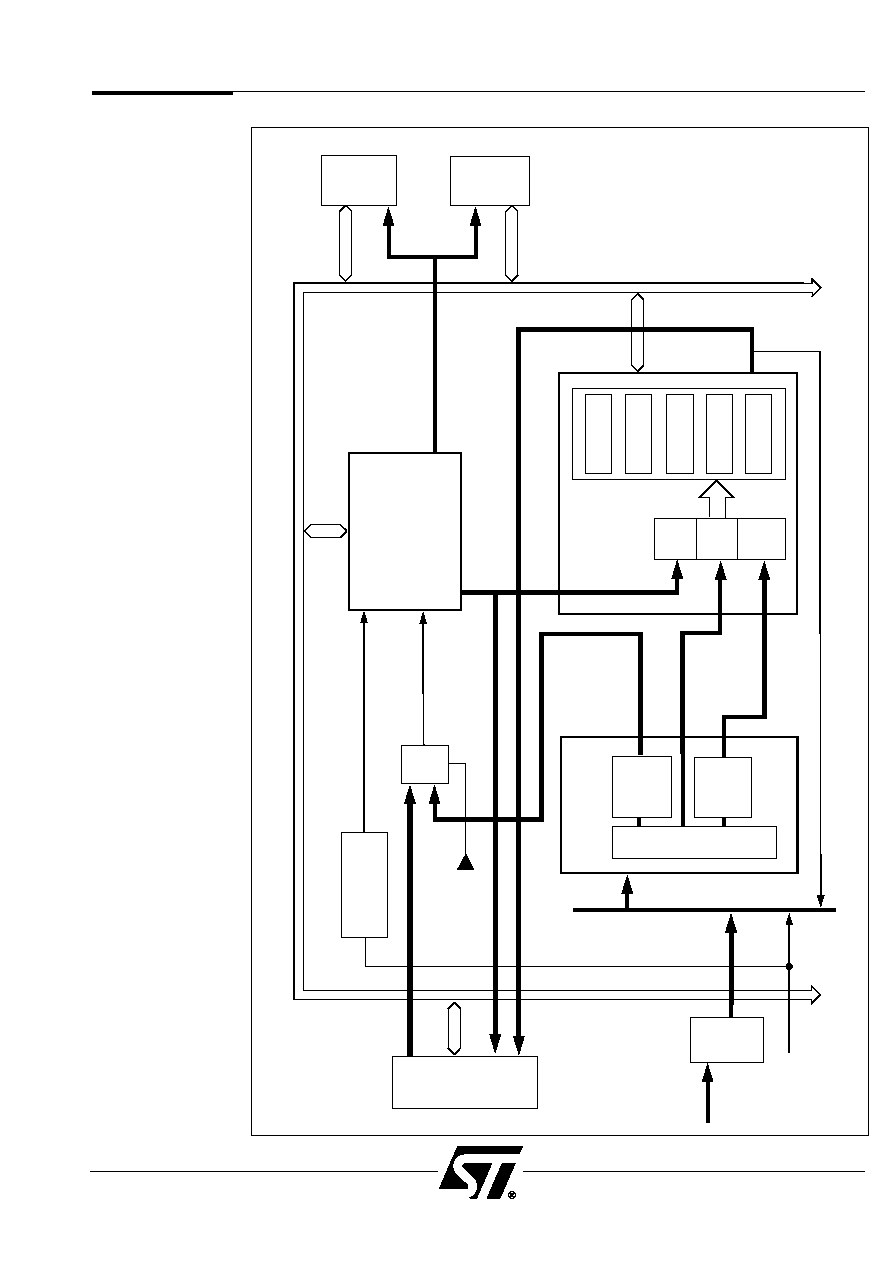
PSD5XX Family
97
Figure 46. Interrupt Controller Interface With Other Internal Blocks
PORT
E
PIN/
MACROCELL
COMMAND
INPUT
PRESCALED CLOCK IN
TIMER
[ 3 : 0
] ≠
IN
MC2INT
[ 6 : 7
]
PT2INT
[ 4 : 5
]
INTR2PLD
MC2TMR
[ 3 : 0
]
CONTROL
BUS
INTRF
CLKIN
ZPLD
INPUT
BUS
AND
ARRAY
TIMER
MACRO-
CELL
INTR
MACRO-
CELL
ADDRESS / DATA / CONTROL BUS
TIMER
/
COUNTER
UNIT
MUX
PROGRAMMABLE
CLOCK
PRESCALAR
PPLD
INTERRUPT
CONTROLLER
INT0
≠
INT3
INT
4
≠
INT5
INT6≠
INT7
INT SENSE
REGISTER
MASK
REGISTER
READ RQST
REGISTER
READ CLEAR
REGISTER
PRIORITY
STATUS REG
TC0
≠TC3
*
TIMER
[ 3:0
] ≠
OUT
INTR
≠
OUT
TIMER
OUTPUTS
PA0 ≠ PA3
TIMER
OUTPUTS
PB0 ≠ PB3
PORT
A
PORT
B
*
TC
: TERMINAL COUNT OF TIMER
Interrupt
Controller
(Cont.)
PSD5XX Family
98
Interrupt Operation
(Cont.)
9.7.1.1 Command Registers
All the eight interrupts can be individually masked using a mask register. Writing "ones"
into these mask bits enables the associated interrupts. RESET masks all interrupts.
Interrupts can also be defined as either LEVEL sensitive or EDGE sensitive using a
sensitivity bit in the interrupt edge/level sensitivity select register.
Tables 29 and 29a give the address map for various port and interrupt Command/Status
Registers. This address offset map is of the host processor, relative to the CSIOP
(Chip Select Input Output Port) i.e., address space allocated by the host Microcontroller to
access all the PSD embedded peripherals.
Address
Register Name
Address
Register Name
Offset
Offset
+D4h
Interrupt Read Clear
+D3h
Interrupt Mask
+D2h
Interrupt Edge/Level
Select
+D1h
Interrupt Request Latch
+D0h
Interrupt Priority Status
Table 29. Offset Address Map of Interrupt Registers
Address
Register Name
Address
Register Name
Offset
Offset
+D5h
Interrupt Read Clear
+D2h
Interrupt Mask
+D3h
Interrupt Edge/Level
Select
+D0h
Interrupt Request Latch
+D1h
Interrupt Priority Status
Table 29a. Offset Address Map of Interrupt Registers
(For 16-Bit Motorola MCUs in 16-Bit Mode. If 8-Bit Mode is selected, use Table 29.)
Bit 7
Bit 6
Bit 5
Bit 4
Bit 3
Bit 2
Bit 1
Bit 0
Mask7
Mask6
Mask5
Mask4
Mask3
Mask2
Mask1
Mask0
Interrupt Mask Register
Bits mask 0
...
mask 7 correspond to interrupt 0
...
interrupt 7.
When these bits are set to
1 = Unmasked
0 = Masked
At RESET these bits initialize as 0 and all interrupts are masked.
The Interrupt Registers listed in Tables 29 and 29a are described below.
Interrupt
Controller
(Cont.)
PSD5XX Family
99
Bit 7
Bit 6
Bit 5
Bit 4
Bit 3
Bit 2
Bit 1
Bit 0
Sense7
Sense6
Sense5
Sense4
Sense3
Sense2
Sense1
Sense0
Interrupt Operation
(cont.)
Interrupt Edge/Level Select Register
Bits sense 0
...
sense 7 correspond to interrupt 0
...
interrupt 7.
When these bits are set to
1 = LEVEL sensitive
0 = EDGE sensitive (positive edge)
At RESET these bits initialize as 0 i.e., all interrupts come up as Edge sensitive.
Interrupt Read Clear Register
This is a read only register. Reading this register during initialization clears all the pending
edge sensitive interrupts.
Bit 7
Bit 6
Bit 5
Bit 4
Bit 3
Bit 2
Bit 1
Bit 0
ir 7
ir 6
ir 5
ir 4
ir 3
ir 2
ir 1
ir 0
Interrupt Request Latch Register
Bits ir 0...ir 7 correspond to interrupt 0 ... interrupt 7.
When any of these bits are set by the interrupt controller to a "1", the corresponding
Interrupt is pending service.
The MCU can read the interrupt request latch which shows the status of all interrupts. The
entire interrupt request latch can be cleared by reading the Interrupt Read Clear Register,
but Level sensitive interrupts cannot be cleared.
Bit 7
Bit 6
Bit 5
Bit 4
Bit 3
Bit 2
Bit 1
Bit 0
*
*
*
*
*
vect 2
vect 1
vect 0
NOTE:
*
= Reserved for future use, bits set to zero.
Interrupt Priority Status Register
The value of these 3 bits (vect2, vect1 and vect0) indicates the highest priority of the
interrupt to be serviced among multiple interrupts pending. Refer to the table above for
priorities of various interrupts. Reading this register clears the highest pending interrupt.
Interrupt
Controller
(Cont.)

PSD5XX Family
100
Interrupt
Controller
(Cont.)
Interrupt Operation
(Cont.)
9.7.2 Input/Output
Interrupt inputs INT4 and INT5 originate from two dedicated PPLD product terms PT2INT4
and PT2INT5. Interrupt inputs INT6 and INT7 originate from the outputs of the PPLD
Macrocells MC2INT6 and MC2INT7 as described in the next section and the remaining
interrupt inputs INT0 through INT3 originate from four Terminal-Count (TC) outputs of the
Counter/Timers. If an External event has to cause an interrupt in the PSD5XX, it has to be
routed through the PPLD.
Regarding output from the Interrupt Controller, whenever an unmasked interrupt occurs, a
Global Interrupt signal is generated. The Global Interrupt signal can be used as a ZPLD
input (INTR2PLD). Refer to Figure 45 for details. It can also be driven off the chip by using
the special-function out capability of Port E (PE2) as INTR_OUT. In either case, the Global
Interrupt indicates to the MCU that an internal PSD5XX interrupt has occurred. Refer to the
section on I/O ports for specific details of setting up the port functions.
9.7.3 PPLD Macrocell
Interrupt inputs INT6 and INT7 originate two dedicated PPLD Macrocells. Each of these
PPLD Macrocells have two product terms as inputs that are inputted into a PPLD Macrocell
as shown in Figure 47. The outputs of both PPLD Macrocells MC2INT6 and MC2INT7 are
either Combinatorial or Register mode. The polarity of the product terms is programmable.
Refer to the section on "ZPLD" for further reference on the PPLD.
9.7.4 Interrupt Flowchart
The flowchart in Figure 48 explains the overall initialization and the servicing
of the interrupts.
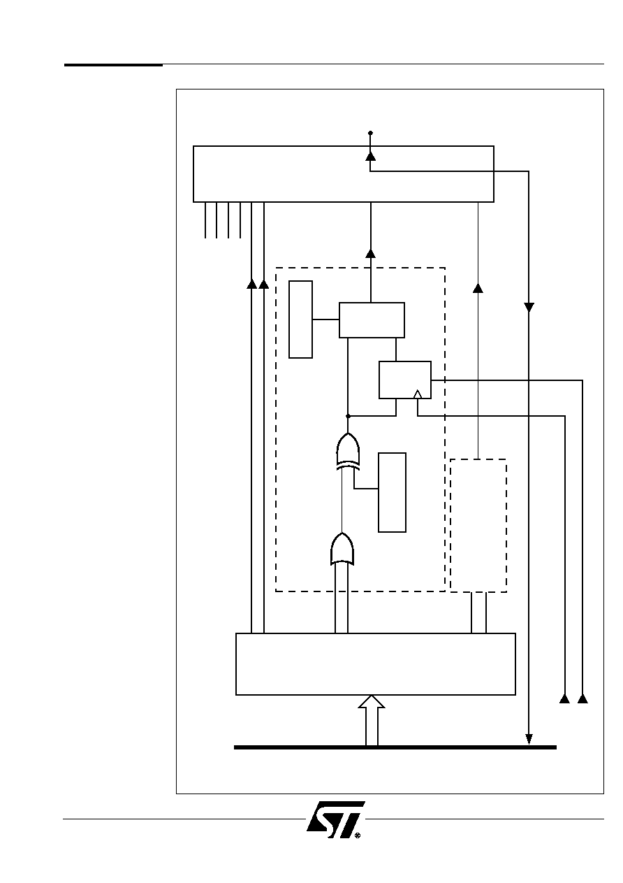
PSD5XX Family
101
Figure 47. PPLD Interrupt Macrocell
AND
ARRAY
PT
PT
PT
PT
PT
PT
CLKIN
RESET
INTR2PLD (INTERNAL FEEDBACK)
SIMILAR
INTERRUPT
MACROCELL
INTERRUPT MACROCELL
POLARITY
SELECT
COMB / REG
SELECT
COMB / REG
SELECT
INTERRUPT
MODULE
PT2INT4
PT2INT5
ZPLD
INPUT
BUS
MUX
DQ
C
MC2INT
7
PT = Product Terms
MC2INT6
INT
7
INT6
PE2
TC0
TC1
TC2
TC3
INT4
INT5
INT2
INT3
INT0
INT1
Interrupt
Controller
(Cont.)
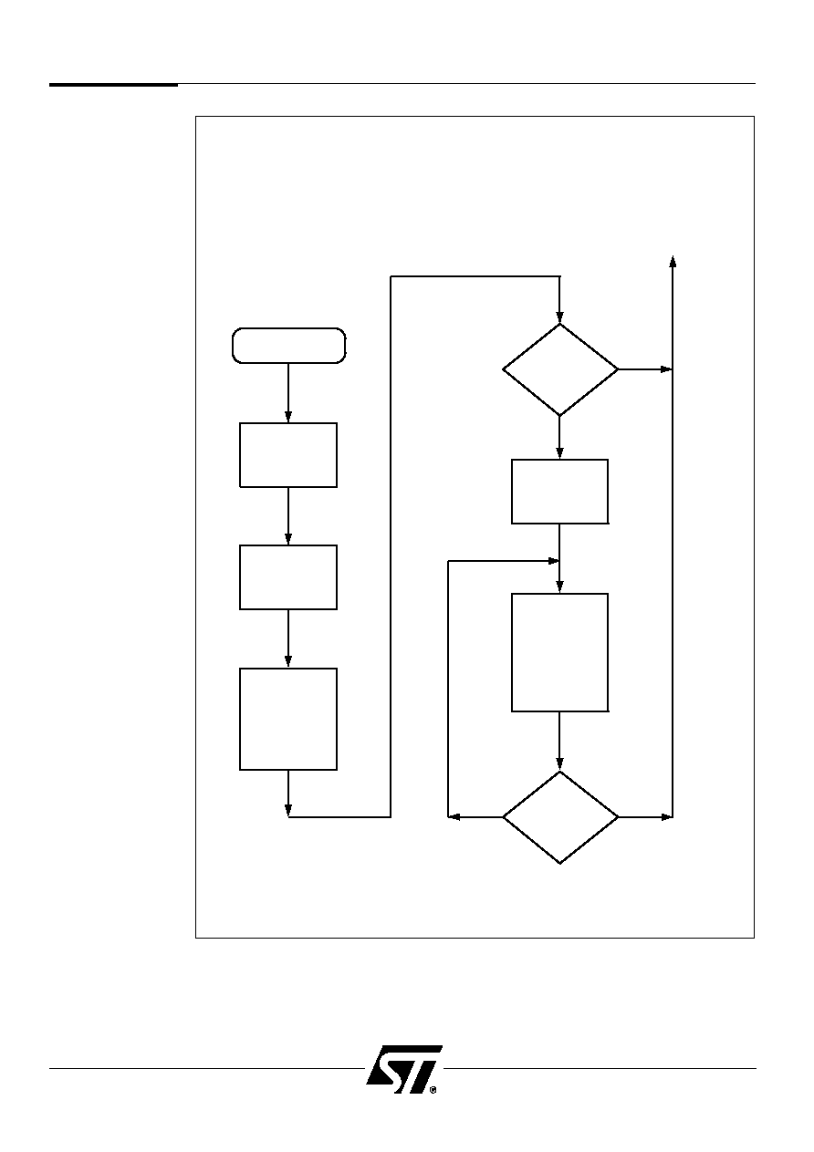
PSD5XX Family
102
Figure 48. Interrupt Flowchart
CONFIGURE
INTERRUPT
SOURCE PLD
AND / OR
TIMER COUNT
i.e. UNMASK
REQD INTRPT
INTERRUPT
OCCURRED ?
DETERMINE
PRIORITY
OF THE
INTERRUPT
KEEP LOW
PRIORITY
INTERRUPTS
PENDING
SERVICE
HIGH PRIORITY
INTERRUPT
ARE
ALL
INTERRUPTS
SERVICED ?
CONTINUE
EXECUTING
MAIN LOOP
UNTIL INTERRUPT
OCCURS
INTERRUPT
INITIALIZATION
CLEAR ALL
PENDING BITS
(READ CLEAR
REGISTER
DEFINE EDGE
OR LEVEL
SENSITIVE
NO
YES
NO
YES
Interrupt
Controller
(Cont.)
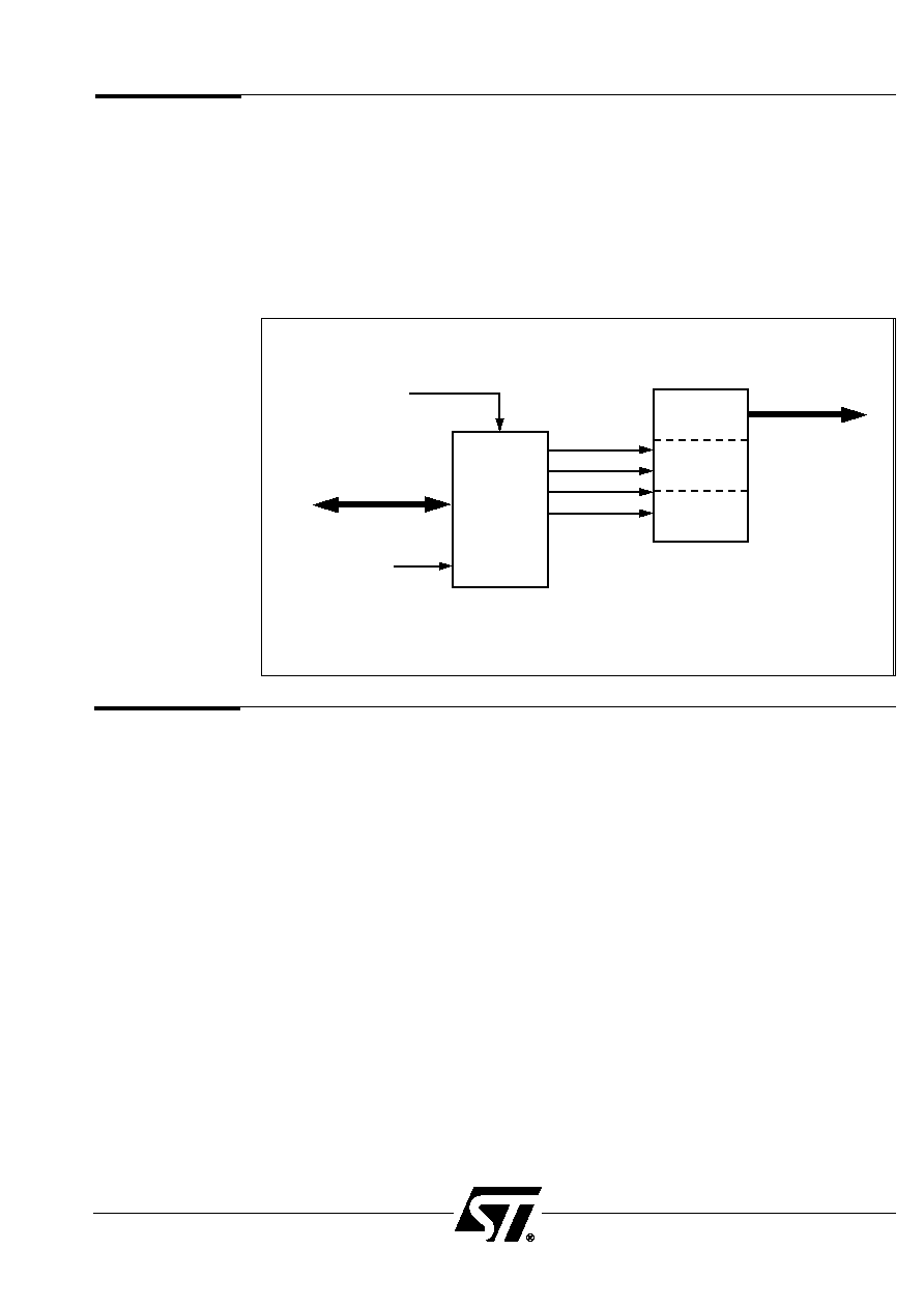
PSD5XX Family
103
The Page Register is 4 bits wide and consists of four D flip flops.The outputs of the Register
(PGR0 ≠ PGR3) are connected to the input bus of the ZPLD. By including the four outputs
as inputs to the DPLD, the addressing capability of the microcontroller is increased by a
factor of 16.
Figure 49 shows the Page Register block diagram. Inputs to the four flip flops are connected
to data bus D0-D3. The output of the Register can be read by the microcontroller. The
Register can operate as an independent register to the microcontroller if page mode is not
implemented.
Figure 49. Page Register
DPLD
RS0
GPLD
PPLD
ZPLD
ES0 ≠ 3
PGR0
PGR1
PGR2
PGR3
R/ W
D0
D0 ≠ D3
D1
D2
D3
Q0
Q1
Q2
Q3
PAGE
REGISTER
RESET
The PSD5XX has a programmable security bit which offers protection from unauthorized
duplication. When the security bit is set, the contents of the EPROM, the PSD5XX
non-volatile configuration bits and ZPLD data are prevented from being read by EPROM
programmers.
The security bit is set through the PSDsoft Software and is embedded in the compiled
output file. The security bit is UV erasable and a secured part can be erased and then
re-programmed.
10.0
Page
Register
11.0
Security
Protection
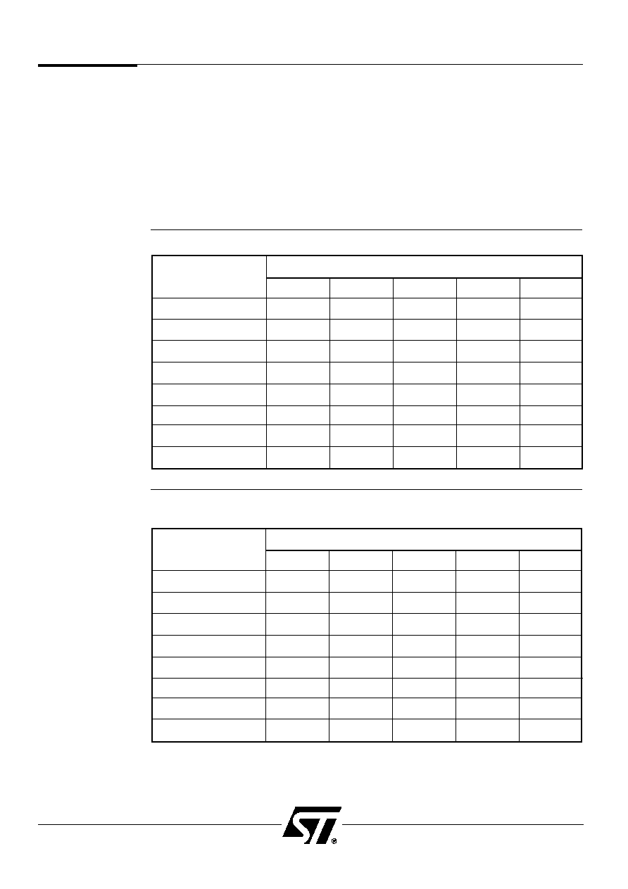
PSD5XX Family
104
12.0
System
Configuration
The CSIOP signal, which is generated by the DPLD, selects the internal I/O devices or
registers. The CSIOP signal takes up 256 bytes of address space and is defined by the user
in the PSDSoft Software. The following is an address offset map for the various devices
relative to the CSIOP base address.
Some Motorola 16-bit microcontrollers have a different data bus/data byte orientation. This
requires a different address offset for the internal PSD5XX I/O devices or registers. Tables
30a and 31a in this section are for this group of microcontrollers which include the
M68HC16, M68302 and M683XX.
The following table is the address map offset of the I/O port registers.
Address Offset
Register Name
Port A
Port B
Port C
Port D
Port E
Data In
00
01
10
11
20
Control
02
03
12
13
22
Data Out
04
05
14
15
24
Direction
06
07
16
17
26
Open Drain
18
19
Special Function
08
09
28
PLD ≠ I/O
0A
0B
2A
Macrocell Out
0C
0D
2C
Table 30. I/O Register Address Offset
Address Offset
Register Name
Port A
Port B
Port C
Port D
Port E
Data In
01
00
11
10
21
Control
03
02
13
12
23
Data Out
05
04
15
14
25
Direction
07
06
17
16
27
Open Drain
19
18
Special Function
09
08
29
PLD ≠ I/O
0B
0A
2B
Macrocell Out
0D
0C
2D
Table 30a. I/O Register Address Offset
(For 16-Bit Motorola MCUs in 16-Bit Mode. If 8-Bit Mode is selected, use Table 30.)

PSD5XX Family
105
System
Configuration
(Cont.)
Register Name
Address
Register Name
Address
Offset
Offset
PAGE REGISTER
E0
INTR. READ CLEAR
D4
INTR. MASK
D3
INTR. EDGE/LEVEL
D2
INTR. REQUEST
D1
INTR. PRIORITY
D0
LATCH
STATUS
VM
C0
PMMR1
B1
PMMR0
B0
STATUS FLAGS
A9
GLOBAL COMMAND
A8
DLCY
A6
SOFTWARE
LOAD/STORE
A5
FREEZE COMMAND
A4
CMD3
A3
CMD2
A2
CMD1
A1
CMD0
A0
CNTR3
9F
CNTR3
9E
CNTR2
9D
CNTR2
9C
CNTR1
9B
CNTR1
9A
CNTR0
99
CNTR0
98
IMG3
97
IMG3
96
IMG2
95
IMG2
94
IMG1
93
IMG1
92
IMG0
91
IMG0
90
Table 31. Other Register Address Offset
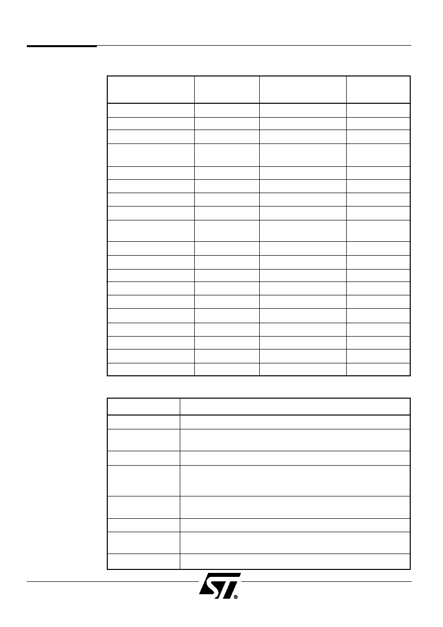
PSD5XX Family
106
System
Configuration
(Cont.)
Register Name
Address
Register Name
Address
Offset
Offset
PAGE REGISTER
E1
INTR. READ CLEAR
D5
INTR. MASK
D2
INTR. EDGE/LEVEL
D3
INTR. REQUEST
D0
INTR. PRIORITY
D1
LATCH
STATUS
VM
C1
PMMR1
B0
PMMR0
B1
STATUS FLAGS
A8
GLOBAL COMMAND
A9
DLCY
A7
SOFTWARE
LOAD/STORE
A4
FREEZE COMMAND
A5
CMD3
A2
CMD2
A3
CMD1
A0
CMD0
A1
CNTR3
9E
CNTR3
9F
CNTR2
9C
CNTR2
9D
CNTR1
9A
CNTR1
9B
CNTR0
98
CNTR0
99
IMG3
96
IMG3
97
IMG2
94
IMG2
95
IMG1
92
IMG1
93
IMG0
90
IMG0
91
Table 31a. Other Register Address Offset
(For 16-Bit Motorola MCUs in 16-Bit Mode. If 8-Bit Mode is selected, use Table 31.)
Register Name
Register Function
Data In
This Register is used to read the input on the port pins.
Control
A
"
0
"
sets the corresponding port pin in Address Out Mode.
A
"
1
"
sets the pin in MCU I/O Mode.
Data Out
Holds the output data in the MCU I/O Mode.
Direction
This register is used to control the data flow in the I/O ports.
A
"
0
"
sets the corresponding pin as an input pin.
A
"
1
"
sets the pin as an output pin.
Open Drain
A
"
0
"
sets the corresponding pin driver as a CMOS driver.
A
"
1
"
sets the pin driver as an Open Drain Driver.
Special Function
A
"
1
"
sets the corresponding port pin as Timer or Interrupt Output.
PLD ≠ I/O
A read only status register; a
"
1
"
indicates the corresponding pin
is configured as a PLD pin.
Macrocell Out
This register holds the outputs of the GPLD macrocells.
Table 32. I/O Register Function
PSD5XX Family
107
System
Configuration
(Cont.)
Register Name
Register Function
PAGE REGISTER
A 4-bit register that supports paging.
INTR. READ
Reading this register clears all the pending edge sensitive
CLEAR
interrupts.
INTR.
Define interrupt input as level or edge sensitive.
EDGE/LEVEL
INTR. MASK
Mask selected interrupt input.
INTR.
A
"
1
"
in the register indicates the corresponding interrupt is
REQUEST LATCH
pending.
INTR.
The register indicates which pending interrupt has the highest
PRIORITY STATUS
priority.
1. Configures the PSD SRAM to be accessed by
"
PSEN
"
as
VM
program space (8031 design).
2. Enable the Peripheral I/O Mode of Port A.
PMMR0
Power management registers; enable the PSD Power Down Mode
PMMR1
and other power saving configurations.
STATUS FLAGS
Counter/Timer Freeze Acknowledge bits.
GLOBAL
Specifies the Counter/Timer operation mode; and to start or stop
COMMAND
the Counter/Timers.
DLCY
Specifies the delay cycles to the Counter/Timers.
SOFTWARE
This register enables a load (to the Counter/Timer) or store
LOAD/STORE
(in the Image Register) operation.
FREEZE
This register disables the timer state-machine before access to the
COMMAND
Image Register is allowed.
CMD3 ≠ 0
Command Registers for the configuration of the Counter/Timers.
CNTR3 ≠ 0
The four 16-bit Counter/Timers.
IMG3 ≠ 0
The Image Registers for CNTR3 ≠ 0.
Table 33. Other Register Function
PSD5XX Family
108
12.1 Reset Input
The reset input to the PSD5XX (RESET) is an active low signal which resets some of
the internal devices and configuration registers. The Timing Diagram in the AC/DC
characterization section shows the reset signal timing requirement. The active low range has
a minimum T1 duration. After the rising edge of RESET, the PSD5XX remains in
reset during T2 range. (See Figure 59). The PSD5XX must be reset at power up before it
can be used.
12.2 ZPLD and Memory During Reset
While the Reset Input is active, the ZPLD generates outputs as defined in the PSDabel
equations. The EPROM and SRAM blocks respond to the microcontroller bus cycle during
reset, but the data is not guaranteed.
12.3 Register Values During and After Reset
Table 34 summarizes the status of the volatile register values during and after reset. The
default values of the volatile registers are "0" after reset.
12.4 ZPLD Macrocell Initialization
The D flip flops in the macrocells in the GPLD can be cleared by:
t
A product term (.RE) defined by the user, in PSDabel or
t
The MACRO-RST (Reset) input, enabled and defined in PSDabel.
The Timer and Interrupt Controller macrocells in the PPLD are always cleared by the
Reset input.
Register Name
Device
Reset State
Control
Port A, B, C, D, E
Set to "0" (Address Out Mode)
Data Out (data or address)
Port A, B, C, D, E
Set to "0"
Direction
Port A, B, C, D, E
Set to "0" ≠ Input Mode
Open Drain
Port C, D
Set to "0" ≠ CMOS Outputs
Page Register
Page Logic
Set to "0"
PMMR0, PMMR1
Power Management Unit
Set to "0"
VM
Volatile Memory
Set to "0"
DLCY
Timer
Set to "0"
CMD0 ≠ CMD3
Timer
Set to "0", Clear
Status Flags
Timer
Set to "0", Clear
Global Command
Timer
Set to "0", Clear
IMG0 ≠ IMG3,
CNTR0 ≠ CNTR3
Timer
Undefined
Interrupt
Interrupt Controller
Set to "0", Disabled
System
Configuration
(Cont.)
Table 34. Registers Reset Values
Port Configuration
Reset
Standby Mode
Port I/O
Input
Unchanged
ZPLD Output
Active
Depend on Inputs to the ZPLD
Address Out
Tri-stated
Not Defined
Data Port
Tri-stated
Tri-stated
Special Function Out
Tri-stated
Depending on Status of
Clock Input to the Counter/Timer
Peripheral I/O
Tri-stated
Tri-state
Table 35. I/O Pin Status During Reset and Standby Mode
PSD5XX Family
109
Symbol
Parameter
Condition
Min
Max
Unit
T
STG
Storage Temperature
CLDCC
≠ 65
+ 150
∞C
PLDCC
≠ 65
+ 125
∞C
Commercial
0
+ 70
∞C
Operating Temperature
Industrial
≠ 40
+ 85
∞C
Military
≠ 55
+ 125
∞C
Voltage on any Pin
With Respect to GND
≠ 0.6
+ 7
V
V
PP
Programming
Supply Voltage
With Respect to GND
≠ 0.6
+ 14
V
V
CC
Supply Voltage
With Respect to GND
≠ 0.6
+ 7
V
ESD Protection
>
2000
V
13.1 Absolute Maximum Ratings
NOTE: Stresses above those listed under Absolute Maximum Ratings may cause permanent
damage to the device. This is a stress rating only and functional operation of the device at
these or any other conditions above those indicated in the operational sections of this
specification is not implied. Exposure to Absolute Maximum Rating conditions for
extended periods of time may affect device reliability.
Type
Temperature
V
CC
V
CC
Tolerance
Speed Grades Available
-70 -90 -15 -20 -25
Commercial
0∞ C to +70∞C
+ 5 V
± 10%
X
X
+ 3 V
± 10%
X
X
Industrial
≠40∞ C to +85∞C
+ 5 V
± 10%
X
+ 3 V
± 10%
X
13.2 Operating Range
Symbol
Parameter
Condition
Min
Typ
Max
Unit
V
CC
Supply Voltage
All Speeds
4.5
5.0
5.5
V
V
CC
Supply Voltage
ZPSD5XXV Versions
2.7
3.0
5.5
V
Only, All Speeds
13.3 Recommended Operating Conditions
13.0
Specifications

PSD5XX Family
110
0
20
60
80
100
120
40
0
10
15
5
20 25
PT100%
PT25%
COMPOSITE FREQUENCY AT PLD INPUTS (MHz)
I
CC
≠ (mA)
TURBO ON
TURBO ON
TURBO OFF
TURBO OFF
Figure 50. ZPLD Typical I
C C
/ Frequency Consumption
(5 V)
Specifications
(cont.)
13.4 AC/DC Parameters
The following tables describe the AC/DC parameters of the PSD5XX family:
t
DC Electrical Specification
t
AC Timing Specification
∑
ZPLD Timing
≠ Combinatorial Delays
≠ Synchronous Clock Mode
≠ Asynchronous Clock Mode
∑
Microcontroller Timing
≠ Read Timing
≠ Write Timing
≠ Peripheral Mode Timing
≠ Power Down and Reset Timing
∑
PSD5XX Specific Timings
≠ Counter/Timer Timing
≠ Interrupt Controller Timing
Following are some issues concerning the parameters presented:
t
In the DC specification, the Supply Current is given for different modes of operation.
Before calculating the total power consumption, determine the percentage of time that
the PSD5XX is in each mode. Also the current is considerably different if the
ZPLD_TURBO bit is "OFF" and EPROM_CMISER is "ON".
t
The AC power component provides the ZPLD, EPROM, SRAM and TIMER mA/MHz
specification. Figure 50 shows the ZPLD mA/MHz as a function of the number
of Product Terms (PT) used.
t
In the ZPLD timing parameters add the required delay when ZPLD_TURBO is "OFF".
t
In the MCU timing specification, add the required time delay when EPROM_CMISER
is "ON".

PSD5XX Family
111
Conditions
Composite PLD input frequency (Freq PLD)
= 8 MHz
MCU ALE frequency (Freq ALE)
= 4 MHz
% EPROM Access
= 80%
% SRAM access
= 15%
% I/O access
= 5% (no additional power above base)
Operational Modes
% Normal
= 10%
% Sleep
= 90%
Number of product terms used
(from fitter report)
= 45 PT
% of total product terms
= 29/118 = 24.6%
Turbo = off
CMiser = on
8-bit bus mode
Calculation (typical numbers used)
I
CC
total = Isleep x %sleep + %normal x
(
I
CC
(ac) + I
CC
(dc)
)
= Isleep x %sleep + % normal x
(
%EPROM x 0.8 mA/MHz x Freq ALE
+ %SRAM x 1.4 mA/MHz x Freq ALE
+ %PLD x (from graph using Freq PLD)
)
= 10 µA x 0.90 + 0.1 x (0.8 x 0.8 mA/MHz x 4 MHz
+ 0.15 x 1.4 mA/MHz x 4 MHz + 0.95 x 23
= 0.9 µA + 0.1 x (2.56 + 0.84 + 21.85)
= 0.9 µA + 0.1 x 25.3
= 0.9 µA + 2.53 mA
= 2.53 mA
Standby current consumption is handled similarly to sleep mode shown above.
Calculation based on I
OUT
= 0 mA.
13.5 Example of PSD5XX Typical Power Calculation at V
CC
= 5.0 V
Specifications
(cont.)
0
10
20
30
40
50
0
10
15
5
20 25
PT100%
PT25%
COMPOSITE FREQUENCY AT PLD INPUTS (MHz)
I
CC
≠ (mA)
TURBO ON
TURBO ON
TURBO OFFTURBO OFF
Figure 51. ZPLD Typical I
C C
/ Frequency Consumption (ZPSD5XXV Devices)
(3 V)
PSD5XX Family
112
Symbol
Parameter
Conditions
Min
Typ
Max
Unit
V
CC
Supply Voltage
All Speeds
4.5
5
5.5
V
V
IH
High Level Input Voltage
4.5 V < V
CC
< 5.5 V
2
V
CC
+ 0.5
V
V
IL
Low Level Input Voltage
4.5 V < V
CC
< 5.5 V
≠0.5
0.8
V
V
IH1
Reset High Level Input Voltage
(Note 1)
0.8 V
CC
V
CC
+ 0.5
V
V
IL1
Reset Low Level Input Voltage
(Note 1)
≠0.5
0.2 V
CC
≠0.1
V
V
HYS
Reset Pin Hysteresis
0.3
V
V
OL
Output Low Voltage
I
OL
= 20 µA, V
CC
= 4.5 V
0.01
0.1
V
I
OL
= 8 mA, V
CC
= 4.5 V
0.15
0.45
V
V
OH
Output High Voltage
I
OH
= ≠20 µA, V
CC
= 4.5 V
4.4
4.49
V
I
OH
= ≠2 mA, V
CC
= 4.5 V
2.4
3.9
V
V
SBY
SRAM Standby Voltage
2.7
V
CC
V
I
SBY
SRAM Standby Current
V
CC
= 0 V
0.5
1
µA
I
IDLE
Idle Current (V
STDBY
Pin)
V
CC
> V
SBY
≠0.1
0.1
µA
V
DF
SRAM Data Retention Voltage
Only on V
STBY
2
V
I
SB1
Standby Supply
Power Down Mode
CSI >V
CC
≠0.3 V (Note 2)
50
100
µA
(PSD5XX)
Current
Sleep Mode
CSI >V
CC
≠0.3 V (Note 3)
20
40
µA
I
SB2
Standby Supply
Power Down Mode
CSI >V
CC
≠0.3 V (Note 2)
25
50
µA
(ZPSD5XX)
Current
Sleep Mode
CSI >V
CC
≠0.3 V (Note 3)
10
20
µA
I
LI
Input Leakage Current
V
SS
< V
IN
< V
CC
≠1
±0.1
1
µA
I
LO
Output Leakage Current
0.45 < V
IN
< V
CC
≠10
± 5
10
µA
ZPLD_TURBO = OFF,
See I
SB1
µA
f = 0 MHz (Note 4)
and I
SB2
I
CC
(DC)
Operating
ZPLD Adder
ZPLD_TURBO = ON,
(Note 4a)
Supply Current
f = 0 MHz
400
700
µA/PT
EPROM Adder
f = 0 MHz
0
mA
SRAM Adder
f = 0 MHz
0
mA
ZPLD AC Adder
Note 4
See
Fig. 50
4.0
mA/MHz
CMiser = ON and
EPROM AC Adder
(8-bit bus mode)
0.8
2
mA/MHz
All other cases
1.8
4
mA/MHz
I
CC
(AC)
CMiser = ON and
(Note 4a)
(8-bit bus mode)
1.4
2.7
mA/MHz
SRAM AC Adder
CMiser = ON and
2
4
mA/MHz
(16-bit bus mode)
CMiser = OFF
3.8
7.5
mA/MHz
13.6 DC Characteristics
(5 V ± 10% Versions)
NOTES: 1. Reset input has hysteresis. V
IL1
is valid at or below 0.2V
CC
≠0.1. V
IH1
is valid at or above 0.8V
CC
.
2. CSI is high or internal Power Down mode is active.
3. Sleep mode bit is set and internal Power Down is active.
4. See ZPLD I
CC
/Frequency Power Consumption graph for details.
4a. I
OUT
= 0 mA.
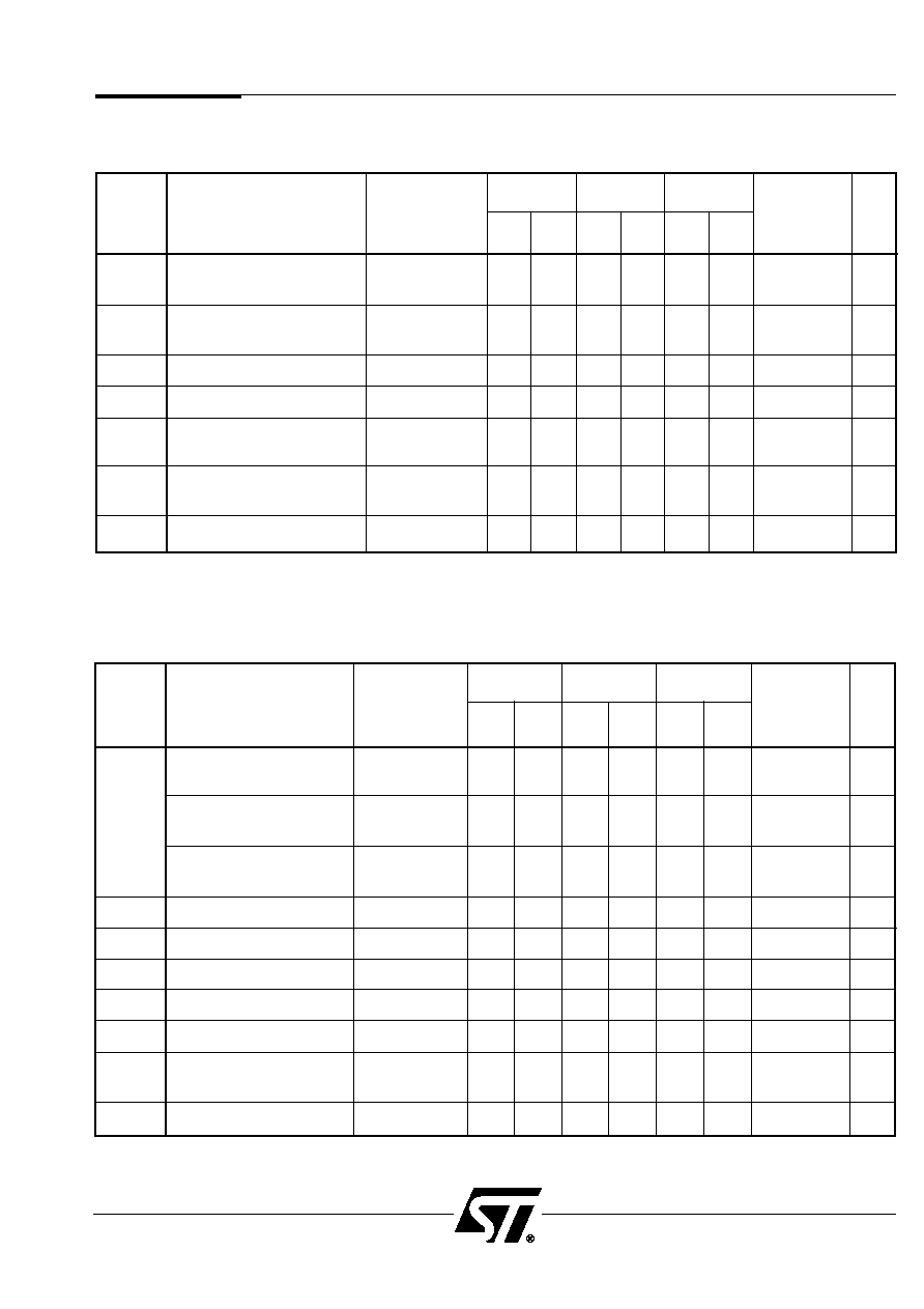
PSD5XX Family
113
-70
-90**
-15
ZPLD_TURBO
Symbol
Parameter
Conditions
Min Max Min Max Min Max
OFF
*
Unit
I/O Input or Feedback to
t
PD
Combinatorial Output
Port B, E
25
30
34
Add 10
ns
t
RPD
Registered Input to
(Note 1)
27
32
36
Add 10
ns
Combinatorial Output
t
EA
Input to Output Enable
Any Input
25
28
32
Add 10
ns
t
ER
Input to Output Disable
Any Input
25
28
32
Add 10
ns
t
ARP
Register Clear or Preset
Any Input
27
30
34
Add 10
ns
Delay
t
ARPW
Register Clear or Preset
Any Input
20
25
29
ns
Pulse Width
t
ARD
Array Delay
16
18
22
ns
Combinatorial Delays
(5 V ± 10% Versions)
NOTE: 1. Ports A, C, D and latched address from ADIO (A0, A1, A8-A15).
*
*
If ZPLD_TURBO is off and the ZPLD is operating above 15 MHz, there is no need to add 10 ns to the timing parameters.
**
The -90 speed is available only on Industrial Temperature Range product.
13.7 AC/DC Parameters ≠ ZPLD Timing Parameters
(5 V ± 10% Versions)
-70
-90**
-15
ZPLD_TURBO
Symbol
Parameter
Conditions
Min
Max
Min
Max
Min
Max
OFF
*
Unit
Maximum Frequency
External Feedback
1/(t
S
+ t
CO
)
30.30
27.03
25.00
MHz
Maximum Frequency
f
MAX
Internal Feedback (f
CNT
)
1/(t
S
+ t
CO
≠10)
43.48
37.04
31.25
MHz
Maximum Frequency
Pipelined Data
1/(t
CH
+ t
CL
)
50.00
41.67
35.71
MHz
t
S
Input Setup Time
Any Input
15
17
20
Add 10
ns
t
H
Input Hold Time
Any Input
0
0
0
0
ns
t
CH
Clock High Time
Clock Input
10
12
15
0
ns
t
CL
Clock Low Time
Clock Input
10
12
15
0
ns
t
CO
Clock to Output Delay
Clock Input
18
20
22
0
ns
t
ARD
Array Delay for Product
Term Expansion
Any Macrocell
16
18
22
0
ns
t
MIN
Minimum Clock Period
t
CH
+ t
CL
20
24
29
0
ns
Synchronous Clock Mode
(5 V ± 10%)
*
*
If ZPLD_TURBO is off and the ZPLD is operating above 15 MHz, there is no need to add 10 ns to the timing parameters.
**
The -90 speed is available only on Industrial Temperature Range product.
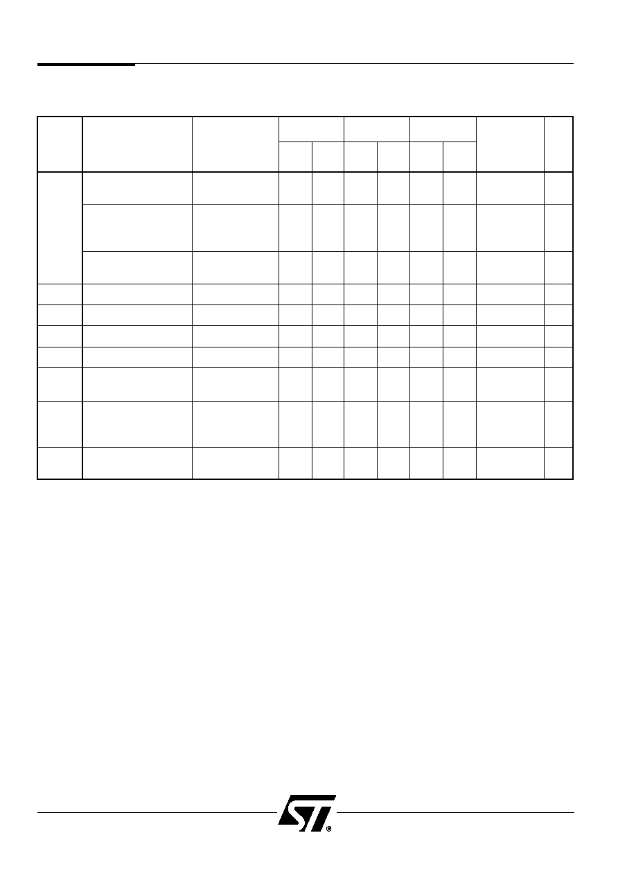
PSD5XX Family
114
-70
-90**
-15
ZPLD_TURBO
Symbol
Parameter
Conditions
Min
Max
Min
Max
Min
Max
OFF
*
Unit
Maximum Frequency
External Feedback
1/(t
SA
+ t
COA
)
26.32
25.00
21.74
MHz
Maximum Frequency
f
MAXA
Internal Feedback
1/(t
S A
+ t
CO A
≠10)
35.71
33.33
27.78
MHz
(f
CNTA
)
(Note 1)
Maximum Frequency
Pipelined Data
1/(t
CH
+ t
CL
)
41.67
41.67
35.71
MHz
t
SA
Input Setup Time
Any Input
8
8
12
Add 10
ns
t
HA
Input Hold Time
Any Input
8
8
12
0
ns
t
CHA
Clock High Time
Any Input
12
12
15
0
ns
t
CLA
Clock Low Time
Any Input
12
12
15
0
ns
t
COA
Clock to Output
Any Input
30
32
37
Add 10
ns
Delay
to Port B
t
ARD
Array Delay for
Product Term
Any Macrocell
16
18
22
0
ns
Expansion
t
MINA
Minimum Clock
Period
1/f
CNT
28
30
43
0
ns
Asynchronous Clock Mode
(5 V ± 10% , Note 1)
AC/DC Parameters ≠ ZPLD Timing Parameters
(5 V ± 10% Versions)
NOTE: 1. Only Port B has asynchronous outputs. Clock into Macrocell Flip Flop is generated by a product term.
*
*
If ZPLD_TURBO is off and the ZPLD is operating above 15 MHz, there is no need to add 10 ns to the timing parameters.
**
The -90 speed is available only on Industrial Temperature Range product.

PSD5XX Family
115
Explanation of AC Symbols for Non ZPLD Timing.
Example:
t
AVLX
Time from Address Valid to ALE Invalid.
A ≠ Address
L ≠ Logic Level Low or ALE
T ≠ R/W
C ≠ Power Down
N ≠ Reset
t ≠ Time
D≠ Input Data
P ≠ Port Signal
V ≠ Valid
E ≠ E
Q ≠ Output Data
X ≠ No Longer a Valid Logic Level
H ≠ Logic Level High
R ≠ WR, UDS, LDS, DS, IORD, PSEN
Z ≠ Float
I ≠ Interrupt
S ≠ Chip Select
-70
-90*
-15
EPROM_CMiser
Symbol
Parameter
Conditions
Min Max Min Max Min Max
ON
Unit
t
LVLX
ALE or AS Pulse Width
18
20
28
0
ns
t
AVLX
Address Setup Time
(Note 4)
5
6
10
0
ns
t
LXAX
Address Hold Time
(Note 4)
7
8
11
0
ns
t
AVQV
Address Valid to Data
Valid
(Note 4)
70
90
150
Add 10
ns
t
SLQV
CS Valid to Data Valid
80
100
150
Add 10
ns
RD to Data Valid
8/16-Bit Bus
(Note 1)
20
32
40
0
ns
t
RLQV
RD to Data Valid 8-Bit
Bus, 8031 Separate
(Note 2)
32
38
45
0
ns
Mode
RD to Data Valid from
(Note 3)
32
38
45
0
ns
Interrupt Controller
t
RHQX
RD Data Hold Time
(Note 1)
0
0
0
0
ns
t
RLRH
RD Pulse Width
(Note 1)
30
32
38
0
ns
t
RHQZ
RD to Data High-Z
(Note 1)
22
25
33
0
ns
t
EHEL
E Pulse Width
30
32
38
0
ns
t
THEH
R/W Setup Time
to Enable
8
10
18
0
ns
t
ELTL
R/W Hold Time After
Enable
0
0
0
0
ns
In 16-Bit Data Bus
20
30
38
0
ns
t
AVPV
Address Input Valid to
Mode (Note 5)
Address Output Delay
In 8-Bit Data Bus
22
32
48
0
ns
Mode (Note 5)
Read Timing
(5 V ± 10% Versions)
NOTES: 1. RD timing has the same timing as PSEN, DS, LDS, UDS signals.
2. RD and PSEN have the same timing for 8031 mode.
3. Read to Data Valid of the Interrupt Request Latch and Interrupt Priority Status. RD timing has the same timing as PSEN, DS,
LDS, UDS signals.
4. Any input used to select an internal PSD5XX function.
5. In multiplexed mode latched address generated from ADIO delay to address output on any Port.
*
The -90 speed is available only on Industrial Temperature Range product.
13.8 Microcontroller Interface ≠ AC/DC Parameters
(5 V ± 10% Versions)
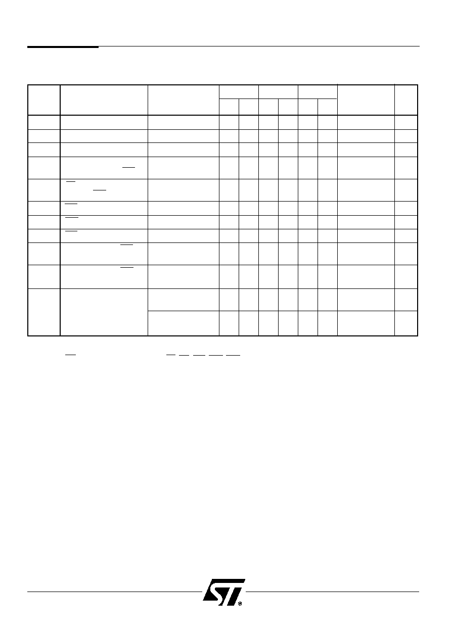
PSD5XX Family
116
-70
-90*
-15
EPROM_CMiser
Symbol
Parameter
Conditions
Min Max Min Max Min Max
ON
Unit
t
LVLX
ALE or AS Pulse Width
18
20
28
ns
t
AVLX
Address Setup Time
(Note 1)
5
6
10
ns
t
LXAX
Address Hold Time
(Note 1)
7
8
11
ns
t
AVWL
Address Valid to
Leading Edge of WR
(Notes 1 and 3)
18
20
30
ns
t
SLWL
CS Valid to Leading
Edge of WR
(Note 3)
22
25
35
ns
t
DVWH
WR Data Setup Time
(Note 3)
12
15
22
ns
t
WHDX
WR Data Hold Time
(Note 3)
5
5
5
ns
t
WLWH
WR Pulse Width
(Note 3)
18
20
28
ns
t
WHAX
Trailing Edge of WR to
Address Invalid
(Note 3)
0
0
0
ns
t
WHPV
Trailing Edge of WR to
Port Output Valid
(Note 3)
25
30
38
ns
In 16-Bit Data Bus
20
30
38
ns
Address Input Valid to
Mode (Note 2)
t
AVPV
Address Output Delay
In 8-Bit Data Bus
22
32
48
ns
Mode (Note 2)
Write Timing
(5 V ± 10%)
Microcontroller Interface ≠ AC/DC Parameters
(5 V ± 10% Versions)
NOTES: 1. Any input used to select an internal PSD5XX function.
2. In multiplexed mode latched address generated from ADIO delay to address output on any Port.
3. WR timing has the same timing as E, DS, LDS, UDS, WRL, WRH signals.
*
The -90 speed is available only on Industrial Temperature Range product.
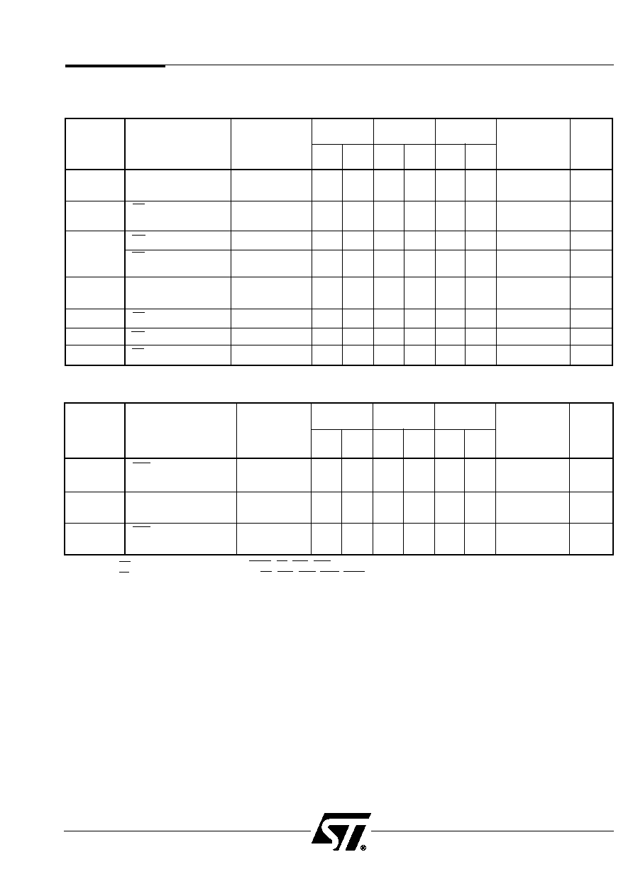
PSD5XX Family
117
-70
-90**
-15
ZPLD_TURBO
Symbol
Parameter
Conditions
Min
Max
Min Max Min Max
OFF
*
Unit
t
AVQV (PA)
Address Valid to
Data Valid
(Note 3)
45
55
62
Add 10
ns
t
SLQV (PA)
CS Valid to Data
Valid
55
55
62
Add 10
ns
RD to Data Valid
(Notes 1 and 4)
22
26
45
0
ns
t
RLQV (PA)
RD to Data Valid
8031 Mode
32
38
45
0
ns
t
DVQV (PA)
Data In to Data Out
Valid
22
22
26
0
ns
t
QXRH (PA)
RD Data Hold Time
(Note 1)
0
0
0
0
ns
t
RLRH (PA)
RD Pulse Width
(Note 1)
25
30
38
0
ns
t
RHQZ (PA)
RD to Data High-Z
(Note 1)
20
25
33
0
ns
Port A Peripheral Data Mode Read Timing
(5 V ± 10%)
-70
-90**
-15
ZPLD_TURBO
Symbol
Parameter
Conditions
Min
Max
Min Max Min
Max
OFF
*
Unit
t
WLQV (PA)
WR to Data
Propagation Delay
(Note 2)
25
27
35
0
ns
t
DVQV (PA)
Data to Port A Data
Propagation Delay
(Note 5)
22
22
26
0
ns
t
WHQZ (PA)
WR Invalid to
Port A Tri-state
(Note 2)
20
25
33
ns
Port A Peripheral Data Mode Write Timing
(5 V ± 10%)
Microcontroller Interface ≠ AC/DC Parameters
(5 V ± 10% Versions)
NOTES: 1. RD timing has the same timing as PSEN, DS, LDS, UDS signals.
2. WR timing has the same timing as E, DS, LDS, UDS, WRL, WRH signals.
3. Any input used to select Port A Data Peripheral Mode.
4. Data is already stable on Port A.
5. Data stable on ADIO pins to data on Port A.
*
*
If ZPLD_TURBO is off and the ZPLD is operating above 15 MHz, there is no need to add 10 ns to the timing parameters.
**
The -90 speed is available only on Industrial Temperature Range product.
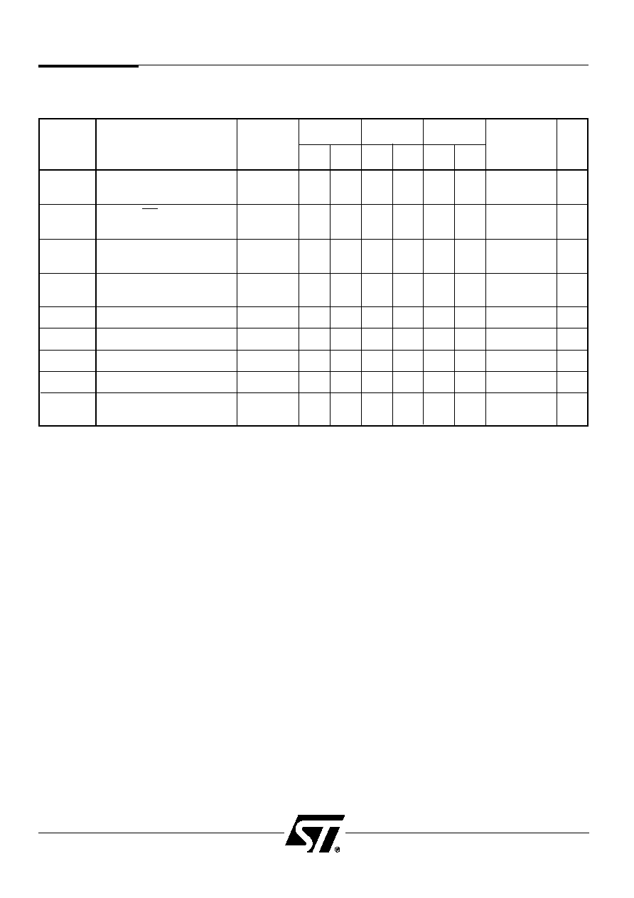
PSD5XX Family
118
Microcontroller Interface ≠ AC/DC Parameters
(5 V ± 10% Versions)
-70
-90**
-15
ZPLD_TURBO
Symbol
Parameter
Conditions
Min Max
Min Max
Min Max
OFF
*
Unit
t
LVDV
ALE Access Time from
Power Down
100
120
150
Add 10
ns
t
LVDV1
ALE or CSI Access Time
from Sleep
120
150
200
0
ns
t
LVDV2
ZPLD Propagation Delay
in Sleep Mode
600
600
600
0
ns
t
LVDV3
ZPLD Recovery Time
after Sleep Mode
250
250
250
0
ns
t
CHCL
APD Clock High Time
Using PE7
10
12
15
0
ns
t
CLCH
APD Clock Low Time
Using PE7
10
12
15
0
ns
f
MAX
APD Maximum Frequency
Using PE7
35.00
30.00
22.00
0
MHz
t
1
RESET Active Low Time
150
200
300
0
ns
t
2
RESET High to
Operational Device
150
200
300
0
ns
Power Down and Reset Timing
(5 V ± 10%)
*
*
If ZPLD_TURBO is off and the ZPLD is operating above 15 MHz, there is no need to add 10 ns to the timing parameters.
**
The -90 speed is available only on Industrial Temperature Range product.

PSD5XX Family
119
-70
-90**
-15
ZPLD_TURBO
Symbol
Parameter
Conditions
Min
Max
Min
Max
Min
Max
OFF
*
Unit
f
MAX
Maximum Frequency
36.00
30.00
22.00
0
MHz
t
CHCL
Clock High Time
10
12
15
0
ns
t
CLCH
Clock Low Time
10
12
15
0
ns
t
CHPV
Clock to Output Delay
28
30
33
0
ns
t
CHPV1
Clock to Watchdog
Output Dealy
50
50
58
Add 10
ns
t
LVCH
Input Setup Time
Relative to Rising
Pin Input
15
17
20
Add 10
Clock Edge
(Note 2)
ns
t
LVCH1
Input Setup Time
PLD
Relative to Rising
Combinatorial
25
27
31
(Note 2)
ns
Clock Edge
Input
t
MIN
Minimum Clock
Period
1/f
MAX
28
33
45
0
ns
Counter/Timer Timing
(5 V ± 10%)
AC/DC Parameters ≠ ZPLD Timing Parameters
(5 V ± 10% Versions)
-70
-90**
-15
ZPLD_TURBO
Symbol
Parameter
Conditions
Min
Max
Min
Max
Min
Max
OFF
*
Unit
t
IVIV
Interrupt Request
Input to Interrupt
Output
(Note 3)
40
50
65
0
ns
t
RXIX
Read Vector to
Interrupt Request
Clear
30
40
55
0
ns
t
ILIL
Interrupt Request
Minimum Pulse
Width
18
20
35
0
ns
t
RLQV
RD to Data Valid
Interrupt Controller
(Note 1)
32
38
45
0
ns
Interrupt Timing
(5 V ± 10%)
NOTES: 1. Read to Data Valid of the Interrupt Request Latch and Interrupt Priority Status. RD timing has the same timing as PSEN, DS,
LDS, UDS signals.
2. For inputs which use PPLD only.
3. This timing is only valid when read to the interrupt request latch and priority status latch are not valid.
*
*
If ZPLD_TURBO is off and the ZPLD is operating above 15 MHz, there is no need to add 10 ns to the timing parameters.
**
The -90 speed is available only on Industrial Temperature Range product.
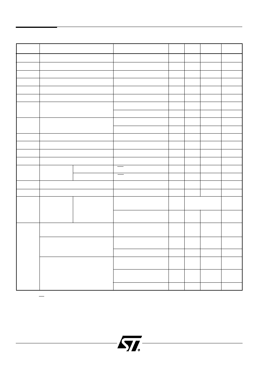
PSD5XX Family
120
Symbol
Parameter
Conditions
Min
Typ
Max
Unit
V
CC
Supply Voltage
All Speeds
2.7
3
5.5
V
V
IH
High Level Input Voltage
2.7 V < V
CC
< 5.5 V
.7 V
CC
V
CC
+.5
V
V
IL
Low Level Input Voltage
2.7 V < V
CC
< 5.5 V
≠0.5
.3 V
CC
V
V
IH1
Reset High Level Input Voltage
(Note 1)
.8 V
CC
V
CC
+.5
V
V
IL1
Reset Low Level Input Voltage
(Note 1)
≠.5
.2 V
CC
≠.1
V
V
HYS
Reset Pin Hysteresis
0.3
V
V
OL
Output Low Voltage
I
OL
= 20 µA, V
CC
= 2.7 V
0.01
0.1
V
I
OL
= 4 mA, V
CC
= 2.7 V
0.15
0.45
V
V
OH
Output High Voltage
I
OH
= ≠20 µA, V
CC
= 2.7 V
2.9
2.99
V
I
OH
= ≠1 mA, V
CC
= 2.7 V
2.4
2.6
V
V
SBY
SRAM Standby Voltage
2.7
V
CC
V
I
SBY
SRAM Standby Current
V
CC
= 0 V
0.5
1
µA
I
IDLE
Idle Current (V
STBY
Pin)
V
CC
> V
SBY
≠0.1
0.1
µA
V
DF
SRAM Data Retention Voltage
Only on V
STBY
2
V
I
SB
Standby Supply
Power Down Mode
CSI >V
CC
≠.3 V (Note 2)
5
15
µA
Current
Sleep Mode
CSI >V
CC
≠.3 V (Note 3)
1
5
µA
I
LI
Input Leakage Current
V
SS
< V
IN
< V
CC
≠1
±.1
1
µA
I
LO
Output Leakage Current
0.45 < V
IN
< V
CC
≠10
± 5
10
µA
ZPLD_TURBO = OFF,
See I
SB
µA
I
CC
(DC)
Operating
f = 0 MHz (Note 4)
(Note 5)
Supply Current
ZPLD Only
ZPLD_TURBO = ON,
f = 0 MHz
200
400
µA/PT
ZPLD AC Base
(Note 4)
See
2.0
mA/MHz
Fig. 51
CMiser = ON
EPROM AC Adder
(8-Bit Bus Mode)
0.4
1.0
mA/MHz
I
CC
(AC)
All Other Cases
0.9
1.7
mA/MHz
(Note 5)
CMiser = ON and
0.7
1.3
mA/MHz
8-Bit Bus Mode
SRAM AC Adder
CMiser = ON and
1
2
mA/MHz
16-Bit Bus MoDe
CMiser = OFF
1.9
3.8
mA/MHz
13.9 DC Characteristics (ZPSD5XXV Versions)
(3.0 V ± 10%)
NOTES:
1. Reset input has hysteresis. V
IL1
is valid at or below .2V
CC
≠.1. V
IH1
is valid at or above .8V
CC
.
2. CSI deselected or internal PD is active.
3. Sleep mode bit is set and internal PD is active.
4. See ZPLD ICC/Frequency Power Consumption graph for details.
5. I
OUT
= 0 mA.

PSD5XX Family
121
-20
-25
ZPLD_TURBO
Symbol
Parameter
Conditions
Min Max Min Max
OFF
*
Unit
I/O Input or Feedback to
t
PD
Combinatorial Output
Port B, E
55
80
Add 20
ns
t
RPD
Registered Input to
(Note 1)
55
85
Add 20
ns
Combinatorial Output
t
EA
Input to Output Enable
Any Input
50
80
Add 20
ns
t
ER
Input to Output Disable
Any Input
50
80
Add 20
ns
t
ARP
Register Clear or Preset Delay
Any Input
55
80
Add 20
ns
t
ARPW
Register Clear or Preset
Any Input
30
60
ns
Pulse Width
t
ARD
Array Delay
33
35
ns
13.10 AC/DC Parameters ≠ ZPLD Timing Parameters
(ZPSD5XXV Versions)
Combinatorial Delays
(3.0 V ± 10%)
NOTE: 1.
Port A and latched address from ADIO (A0, A1, A8 ≠ A15).
*
NOTE: If ZPLD_TURBO is off and the ZPLD is operating above 15 MHz, there is no need to add 20 ns to the timing parameters.
-20
-25
ZPLD_TURBO
Symbol
Parameter
Conditions
Min
Max
Min
Max
OFF
*
Unit
Maximum Frequency
External Feedback
1/(t
S
+ t
CO
)
28.57
11.11
MHz
Maximum Frequency
f
MAX
Internal Feedback (f
CNT
)
1/(t
S
+ t
CO
≠10)
17.24
12.50
MHz
Maximum Frequency
Pipelined Data
1/(t
CH
+ t
CL
)
31.25
18.52
MHz
t
S
Input Setup Time
Any Input
45
60
Add 20
ns
t
H
Input Hold Time
Any Input
0
0
0
ns
t
CH
Clock High Time
Clock Input
16
27
0
ns
t
CL
Clock Low Time
Clock Input
16
27
0
ns
t
CO
Clock to Output Delay
Clock Input
30
33
0
ns
t
ARD
Array Delay for Product
Term Expansion
Any Macrocell
24
35
0
ns
t
MIN
Minimum Clock Period
t
CH
+ t
CL
30
30
0
ns
Synchronous Clock Mode
(3.0 V ± 10%)
*
NOTE: If ZPLD_TURBO is off and the ZPLD is operating above 15 MHz, there is no need to add 20 ns to the timing parameters.

PSD5XX Family
122
-20
-25
ZPLD_TURBO
Symbol
Parameter
Conditions
Min
Max
Min
Max
OFF
*
Unit
Maximum Frequency
External Feedback
1/(t
SA
+ t
COA
)
14.49
11.11
MHz
Maximum Frequency
1/(t
S A
+ t
CO A
≠10)
16.95
12.50
MHz
f
MAXA
Internal Feedback (f
CNTA
)
(Note 1)
Maximum Frequency
Pipelined Data
1/(t
CH
+ t
CL
)
31.25
18.52
MHz
t
SA
Input Setup Time
Any Input
13
30
Add 20
ns
t
HA
Input Hold Time
Any Input
13
30
0
ns
t
CHA
Clock High Time
Any Input
25
27
0
ns
t
CLA
Clock Low Time
Any Input
16
27
0
ns
t
COA
Clock to Output Delay
Any Input to Port B
56
60
Add 20
ns
t
ARD
Array Delay for Product
Term Expansion
Any Macrocell
33
35
0
ns
t
MINA
Minimum Clock Period
1/f
CNT
59
80
0
ns
Asynchronous Clock Mode
(3.0 V ± 10%, Note 1)
AC/DC Parameters ≠ ZPLD Timing Parameters
(ZPSD5XXV Versions)
NOTE: 1. Only Port B has asynchronous outputs. Clock into macrocell Flip Flop is generated by a product term.
*
NOTE: If ZPLD_TURBO is off and the ZPLD is operating above 15 MHz, there is no need to add 20 ns to the timing parameters.
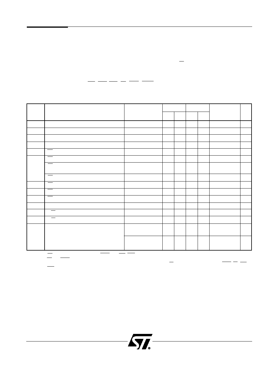
PSD5XX Family
123
-20
-25
EPROM_CMiser
Symbol
Parameter
Conditions
Min Max Min Max
ON
Unit
t
LVLX
ALE or AS Pulse Width
30
30
0
ns
t
AVLX
Address Setup Time
(Note 4)
12
15
0
ns
t
LXAX
Address Hold Time
(Note 4)
12
17
0
ns
t
AVQV
Address Valid to Data Valid
(Note 4)
200
250
Add 20
ns
t
SLQV
CS Valid to Data Valid
200
275
Add 20
ns
RD to Data Valid 8/16-Bit Bus
(Note 1)
50
80
0
ns
RD to Data Valid 8-Bit Bus,
t
RLQV
8031 Separate Mode
(Note 2)
57
90
0
ns
RD to Data Valid from Interrupt Controller (Note 3)
50
90
0
ns
t
RHQX
RD Data Hold Time
(Note 1)
0
0
0
ns
t
RLRH
RD Pulse Width
(Note 1)
40
70
0
ns
t
RHQZ
RD to Data High-Z
(Note 1)
45
45
0
ns
t
EHEL
E Pulse Width
40
70
0
ns
t
THEH
R/W Setup Time to Enable
20
22
0
ns
t
ELTL
R/W Hold Time After Enable
0
0
0
ns
In 16-Bit Data Bus
t
AVPV
Address Input Valid to
Mode (Note 5)
40
60
0
ns
Address Output Delay
In 8-Bit Data Bus
Mode (Note 5)
50
60
0
ns
Read Timing
(3.0 V ± 10%)
Explanation of AC Symbols for Non ZPLD Timing.
Example:
t
AVLX
Time from Address Valid to ALE Invalid.
A ≠ Address
L ≠ Logic Level Low or ALE
T ≠ R/W
C ≠ Power Down
N ≠ Reset
t ≠ Time
D≠ Input Data
P ≠ Port Signal
V ≠ Valid
E ≠ E
Q ≠ Output Data
X ≠ No Longer a Valid Logic Level
H ≠ Logic Level High
R ≠ WR, UDS, LDS, DS, IORD, PSEN
Z ≠ Float
I ≠ Interrupt
S ≠ Chip Select
13.11 Microcontroller Interface ≠AC/DC Parameters
(ZPSD5XXV Versions)
NOTES: 1. RD timing has the same timing as PSEN, DS, LDS, UDS signals (in 8031 combined mode).
2. RD and PSEN have the same timing for 8031 separate mode.
3. Read to Data Valid of the Interrupt Request Latch and Interrupt Priority Status. RD timing has the same timing as PSEN, DS, LDS,
UDS signals.
4. Any input used to select an internal ZPSD5XX function.
5. In multiplexed mode latched address generated from ADIO delay to address output on any Port.
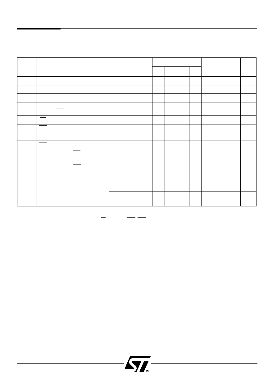
NOTES: 1. Any input used to select an internal ZPSD5XX function.
2. In multiplexed mode latched address generated from ADIO delay to address output on any Port.
3. WR timing has the same timing as E, DS, LDS, UDS, WRL, WRH signals.
PSD5XX Family
124
-20
-25
EPROM_CMiser
Symbol
Parameter
Conditions
Min Max Min Max
ON
Unit
t
LVLX
ALE or AS Pulse Width
30
30
ns
t
AVLX
Address Setup Time
(Note 1)
12
15
ns
t
LXAX
Address Hold Time
(Note 1)
12
17
ns
t
AVWL
Address Valid to Leading
Edge of WR
(Notes 1 and 3)
35
50
ns
t
SLWL
CS Valid to Leading Edge of WR
(Note 3)
40
60
ns
t
DVWH
WR Data Setup Time
(Note 3)
25
35
ns
t
WHDX
WR Data Hold Time
(Note 3)
5
10
ns
t
WLWH
WR Pulse Width
(Note 3)
30
30
ns
t
WHAX
Trailing Edge of WR to Address
Invalid
(Note 3)
0
0
ns
t
WHPV
Trailing Edge of WR to Port
Output Valid
(Note 3)
50
60
ns
In 16-Bit Data Bus
40
60
ns
Address Input Valid to
Mode (Note 2)
t
AVPV
Address Output Delay
In 8-Bit Data Bus
50
60
ns
Mode (Note 2)
Write Timing
(3.0 V ± 10%)
Microcontroller Interface ≠ AC/DC Parameters
(ZPSD5XXV Versions)
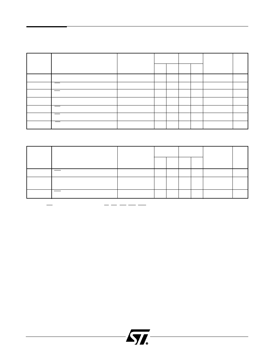
PSD5XX Family
125
-20
-25
ZPLD_TURBO
Symbol
Parameter
Conditions
Min Max Min Max
OFF
*
Unit
t
WLQV (PA)
WR to Data Propagation Delay
(Note 2)
60
60
0
ns
t
DVQV (PA)
Data to Port A Data
Propagation Delay
(Note 5)
40
50
0
ns
t
WHQZ (PA)
WR Invalid to Port A Tri-state
(Note 2)
35
60
0
ns
Port A Peripheral Data Mode Write Timing
(3.0 V ± 10%)
Microcontroller Interface ≠ AC/DC Parameters
(ZPSD5XXV Versions)
-20
-25
ZPLD_TURBO
Symbol
Parameter
Conditions
Min Max Min Max
OFF
*
Unit
t
AVQV (PA)
Address Valid to Data Valid
(Note 3)
95
120
Add 20
ns
t
SLQV (PA)
CS Valid to Data Valid
100
120
Add 20
ns
t
RLQV (PA)
RD to Data Valid
(Notes 1 and 4)
50
90
0
ns
t
DVQV (PA)
Data In to Data Out Valid
35
50
0
ns
t
QXRH (PA)
RD Data Hold Time
(Note 1)
0
0
0
ns
t
RLRH (PA)
RD Pulse Width
(Note 1)
40
70
0
ns
t
RHQZ (PA)
RD to Data High-Z
(Note 1)
35
60
0
ns
Port A Peripheral Data Mode Read Timing
(3.0 V ± 10%)
NOTES: 1. Any input used to select an internal ZPSD5XX function.
2. WR timing has the same timing as E, DS, LDS, UDS, WRL, WRH signals.
3. Any input used to select Port A Data Peripheral Mode.
4. Data is already stable on Port A.
5. Data stable on ADIO pins to data on Port A.
*
NOTE: If ZPLD_TURBO is off and the ZPLD is operating above 15 MHz, there is no need to add 20 ns to the timing parameters.
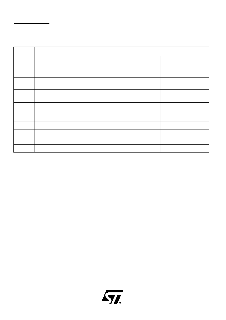
PSD5XX Family
126
-20
-25
ZPLD_TURBO
Symbol
Parameter
Conditions
Min
Max
Min
Max
OFF
*
Unit
t
LVDV
ALE Access Time from
Power Down
170
250
Add 20
ns
t
LVDV1
ALE or CSI Access Time
from Sleep
200
250
0
ns
t
LVDV2
ZPLD Propagation Delay
in Sleep Mode
600
900
0
ns
t
LVDV3
ZPLD Recovery Time after
Sleep Mode
250
400
0
ns
t
CHCL
APD Clock High Time
Using PE7
16
27
0
ns
t
CLCH
APD Clock Low Time
Using PE7
16
27
0
ns
f
MAX
APD Maximum Frequency
Using PE7
20.00
18.52
0
MHz
t
1
RESET Active Low Time
300
400
0
ns
t
2
RESET High to Operational Device
300
400
0
ns
Power Down and Reset Timing
(3.0 V ± 10%)
Microcontroller Interface ≠ AC/DC Parameters
(ZPSD5XXV Versions)
*
NOTE: If ZPLD_TURBO is off and the ZPLD is operating above 15 MHz, there is no need to add 20 ns to the timing parameters.
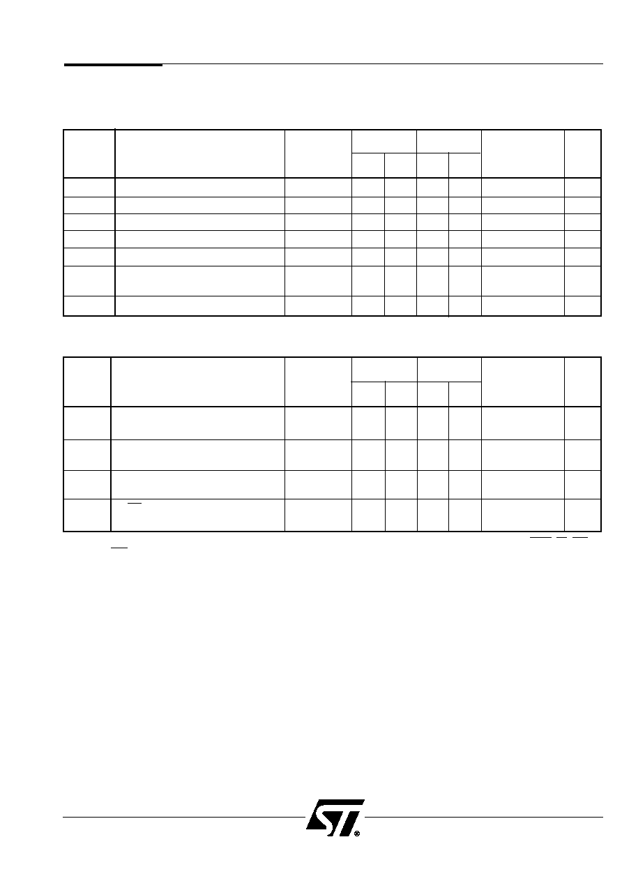
PSD5XX Family
127
-20
-25
ZPLD_TURBO
Symbol
Parameter
Conditions
Min
Max
Min
Max
OFF
*
Unit
t
IVIV
Interrupt Request Input to
Interrupt Output
(Note 3)
70
120
0
ns
t
RXIX
Read Vector to Interrupt
Request Clear
60
100
0
ns
t
ILIL
Interrupt Request Minimum
Pulse Width
40
45
0
ns
t
RLQV
RD to Data Valid Interrupt
Controller
(Note 1)
50
90
0
ns
-20
-25
ZPLD_TURBO
Symbol
Parameter
Conditions
Min
Max
Min
Max
OFF
*
Unit
f
MAX
Maximum Frequency
20.00
12.50
0
MHz
t
CHCL
Clock High Time
16
22
0
ns
t
CLCH
Clock Low Time
16
22
0
ns
t
CHPV
Clock to Output Delay
50
55
0
ns
t
CHPV1
Clock to Watchdog Output Delay
90
100
Add 20
ns
t
LVCH
Input Setup Time Relative
Add 20
to Rising Level Clock
Any Input
45
60
(Note 2)
ns
t
MIN
Minimum Clock Period
1/f
MAX
50
80
0
ns
NOTES: 1. Read to Data Valid of the Interrupt Request Latch and Interrupt Priority Status. RD timing has the same timing as PSEN, DS, LDS,
UDS signals.
2. For inputs which use PPLD only.
3. This timing is only valid when read to the interrupt request latch and priority status latch are not valid.
*
If ZPLD_TURBO is off and the ZPLD is operating above 15 MHz, there is no need to add 20 ns to the timing parameters.
Counter/Timer Timing
(3.0 V ± 10%)
Interrupt Timing
(3.0 V ± 10%)
AC/DC Parameters ≠ ZPLD Timing Parameters
(ZPSD5XXV Versions)
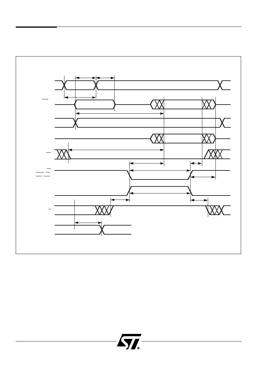
PSD5XX Family
128
Figure 52. Read Timing
tAVLX
tLXAX
tLVLX
tAVQV
tSLQV
tRLQV
tRHQX
tRHQZ
tELTL
tEHEL
tRLRH
tTHEH
tAVPV
ADDRESS
VALID
ADDRESS
VALID
DATA
VALID
DATA
VALID
ADDRESS OUT
ALE /AS
A /D (BHE)
MULTIPLEXED
BUS
ADDRESS
(BHE/SIZ0)
NON-MULTIPLEXED
BUS
DATA
NON-MULTIPLEXED
BUS
CSI
RD
(PSEN, DS)
(LDS, UDS)
E
R / W
14.0 Timing Diagrams
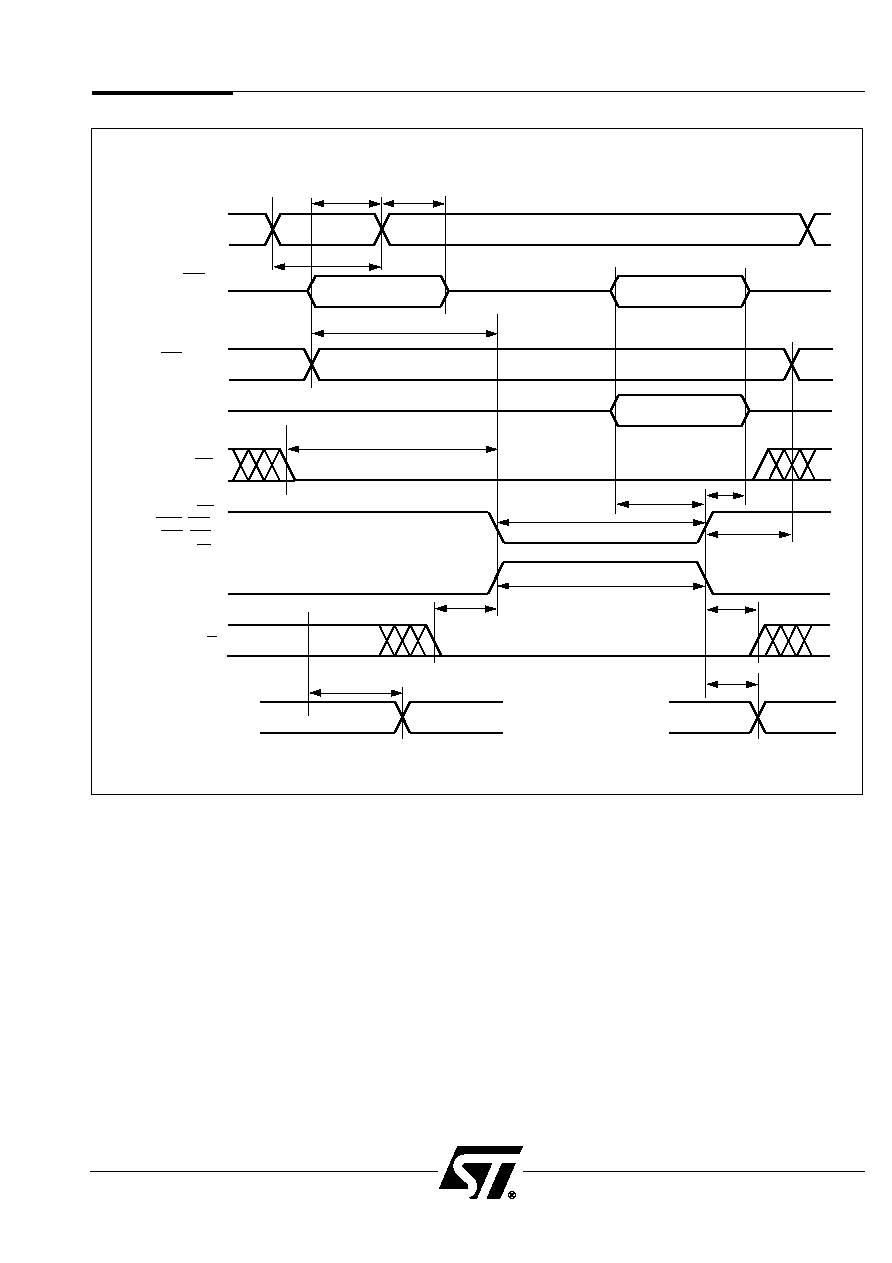
PSD5XX Family
129
Figure 53. Write Timing
tAVLX
tLXAX
tLVLX
tAVWL
tSLWL
tWHDX
tWHAX
tELTL
tEHEL
tWLWH
tDVWH
tTHEH
tAVPV
ADDRESS
VALID
ADDRESS
VALID
DATA
VALID
DATA
VALID
ADDRESS OUT
tWHPV
STANDARD
MCU I/O OUT
ALE / AS
A /D (BHE)
MULTIPLEXED
BUS
ADDRESS
(BHE, SIZ0)
NON-MULTIPLEXED
BUS
DATA
NON-MULTIPLEXED
BUS
CSI
WR
(WRH, WRL)
(LDS, UDS)
(DS)
E
R / W

PSD5XX Family
130
Figure 54. Peripheral I/O Read Timing
tQXRH (PA)
tRLQV (PA)
tRLRH (PA)
tDVQV (PA)
tRHQZ (PA)
tSLQV (PA)
tAVQV (PA)
ADDRESS
DATA VALID
ALE /AS
A /D BUS
RD
DATA ON PORT A
CSI
Figure 55. Peripheral I/O Write Timing
tDVQV (PA)
tWLQL (PA)
tWHQZ (PA)
ADDRESS
DATA OUT
A / D BUS
WR
PORT A
DATA OUT
ALE /AS
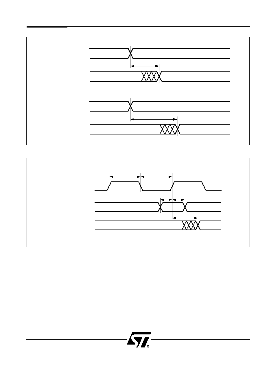
PSD5XX Family
121
Figure 56. Combinatorial Timing ≠ ZPLD
tPD
tRPD
INPUT
(FROM PORT A)
ANY OUTPUT
ANY
OUTPUT
INPUT
(FROM PORT B, C, D, E)
Figure 57. Synchronous Clock Mode Timing ≠ ZPLD
tCH
tCL
tCO
tH
tS
CLKIN
INPUT
REGISTERED
OUTPUT
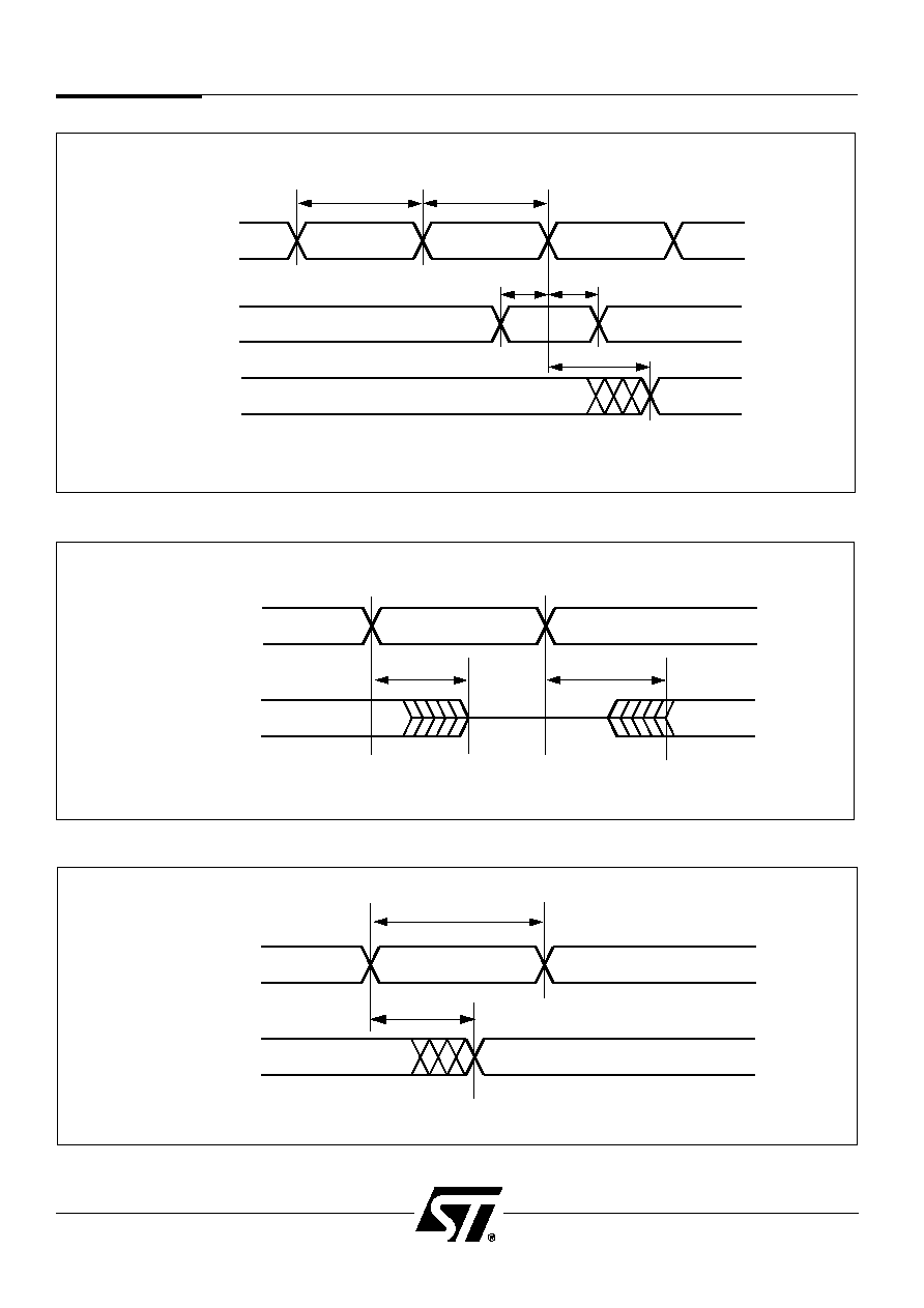
PSD5XX Family
132
Figure 58. Asynchronous Clock Mode Timing (Product-Term Clock, PB Macrocell Only)
Figure 59. Input to Output Disable/Enable
Figure 60. Asynchronous Reset/Preset
tER
tEA
INPUT
INPUT TO
OUTPUT
ENABLE/DISABLE
tARP
REGISTER
OUTPUT
tARPW
RESET/PRESET
INPUT
tCHA
tCLA
tCOA
tHA
tSA
CLOCK
INPUT
REGISTERED
OUTPUT
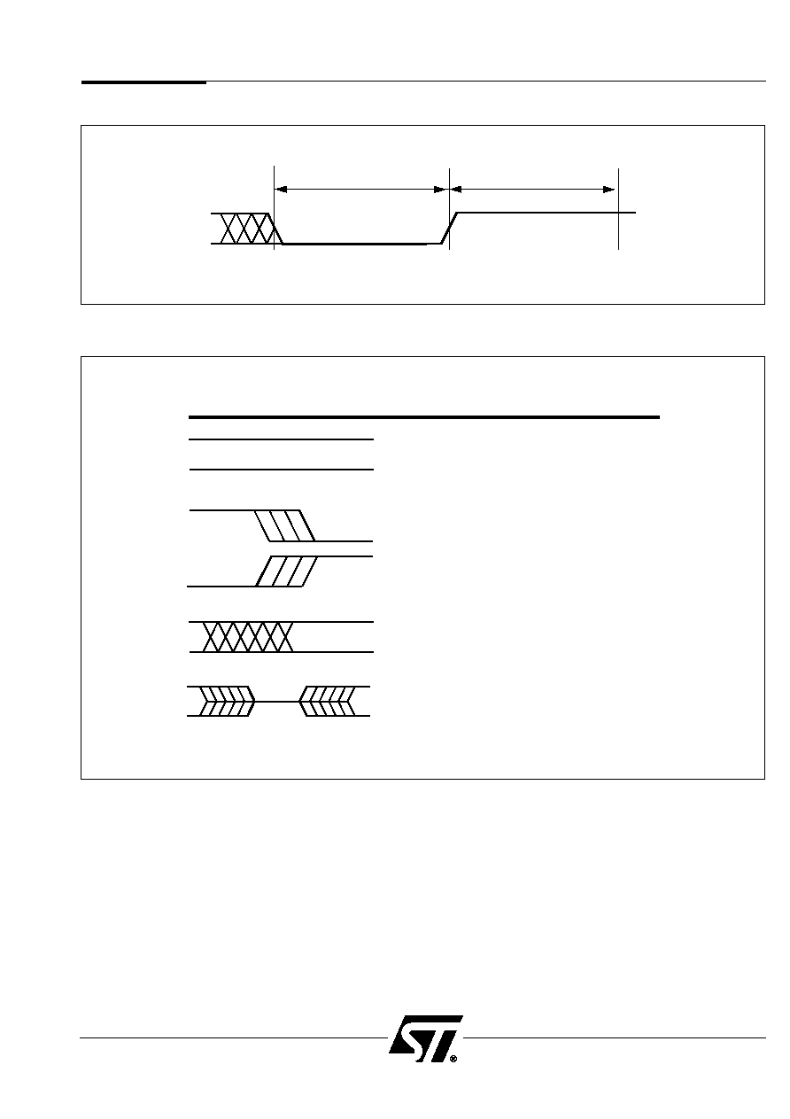
PSD5XX Family
133
Figure 61. Reset Timing
T1
T2
Figure 62. Key to Switching Waveforms
WAVEFORMS
INPUTS
OUTPUTS
STEADY INPUT
MAY CHANGE FROM
HI TO LO
MAY CHANGE FROM
LO TO HI
DON'T CARE
OUTPUTS ONLY
STEADY OUTPUT
WILL BE CHANGING
FROM HI TO LO
WILL BE CHANGING
LO TO HI
CHANGING, STATE
UNKNOWN
CENTER LINE IS
TRI-STATE
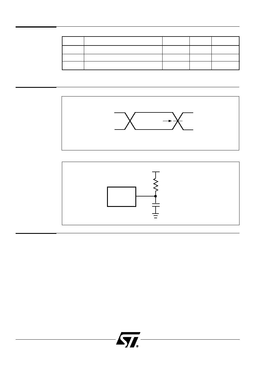
PSD5XX Family
134
Symbol
Parameter
1
Conditions Typical
2
Max Unit
C
IN
Capacitance (for input pins only)
V
IN
= 0 V
4
6
pF
C
OUT
Capacitance (for input/output pins)
V
OUT
= 0 V
8
12
pF
C
VPP
Capacitance (for WR/V
PP
or R/W/V
PP
)
V
PP
= 0 V
18
25
pF
NOTES: 1. These parameters are only sampled and are not 100% tested.
2. Typical values are for T
A
= 25∞C and nominal supply voltages.
T
A
= 25 ∞C, f = 1 MHz
15.0
Pin
Capacitance
Figure 63. AC Testing Input/Output Waveform
Figure 64. AC Testing Load Circuit
17.0
Erasure and
Programming
3.0V
0V
TEST POINT
1.5V
DEVICE
UNDER TEST
2.01 V
195
C
L
= 30 pF
(INCLUDING
SCOPE AND JIG
CAPACITANCE)
To clear all locations of their programmed contents, expose the window packaged device
to an ultra-violet light source. A dosage of 30 W second/cm
2
is required (40 W second/cm
2
for ZPSD5XXV versions). This dosage can be obtained with exposure to a wavelength of
2537 ≈ and intensity of 12000 µW/cm
2
for 40 to 45 minutes (55 to 60 minutes for
ZPSD5XXV versions). The device should be about 1 inch from the source, and all filters
should be removed from the UV light source prior to erasure.
The PSD5XX and similar devices will erase with light sources having wavelengths shorter
than 4000 ≈. Although the erasure times will be much longer than with UV sources at 2537
≈, exposure to fluorescent light and sunlight eventually erases the device. For maximum
system reliability, these sources should be avoided. If used in such an environment, the
package windows should be covered by an opaque substance.
Upon delivery from WSI, or after each erasure, the PSD5XX device has all bits in the PAD
and EPROM in the "1" or high state. The configuration bits are in the "0" or low state. The
code, configuration, and PAD MAP data are loaded through the procedure of programming
Information for programming the device is available directly from WSI. Please contact your
local sales representative.
16.0
AC Testing

PSD5XX Family
135
68-Pin
68-Pin
Pin No.
PLDCC/CLDCC
Pin No.
PLDCC/CLDCC
Package
Package
1
GND
35
GND
2
ADIO_7
36
PE2
3
ADIO_6
37
PE1
4
ADIO_5
38
PE0
5
ADIO_4
39
CSI
6
ADIO_3
40
RESET
7
ADIO_2 41
RD
8
ADIO_1
42
CLKIN
9
ADIO_0 43
PB7
10
PC7
44
PB6
11
PC6
45
PB5
12
PC5
46
PB4
13
PC4
47
PB3
14
PC3
48
PB2
15
PC2
49
PB1
16
PC1
50
PB0
17
PC0
51
GND
18
VCC
52
VCC
19
GND
53
PD7
20
PA7
54
PD6
21
PA6
55
PD5
22
PA5
56
PD4
23
PA4
57
PD3
24
PA3
58
PD2
25
PA2
59
PD1
26
PA1
60
PD0
27
PA0
61
ADIO_15
28
Vstby
62
ADIO_14
29
WR
63
ADIO_13
30
PE7
64
ADIO_12
31
PE6
65
ADIO_11
32
PE5
66
ADIO_10
33
PE4
67
ADIO_9
34
PE3
68
ADIO_8
18.0
PSD5XX
Pin
Assignments
PSD5XX Family
136
80-Pin
80-Pin
Pin No.
TQFP
Pin No.
TQFP
Package
Package
1
PC7
41
PB7
2
PC6
42
PB6
3
PC5
43
PB5
4
PC4
44
PB4
5
PC3
45
PB3
6
PC2
46
PB2
7
PC1
47
PB1
8
PC0
48
PB0
9
V
CC
49
GND
10
V
CC
59
GND
11
GND
51
V
CC
12
GND
52
V
CC
13
PA7
53
PD7
14
PA6
54
PD6
15
PA5
55
PD5
16
PA4
56
PD4
17
PA3
57
PD3
18
PA2
58
PD2
19
PA1
59
PD1
20
PA0
60
PD0
21
NC
61
NC
22
NC
62
ADIO_15
23
Vstdby
63
ADIO_14
24
WR
64
ADIO_13
25
PE7
65
ADIO_12
26
PE6
66
ADIO_11
27
PE5
67
ADIO_10
28
PE4
68
ADIO_9
29
PE3
69
ADIO_8
30
GND
70
GND
31
GND
71
GND
32
PE2
72
ADIO_7
33
PE1
73
ADIO_6
34
PE0
74
ADIO_5
35
CSI
75
ADIO_4
36
RESET
76
ADIO_3
37
RD
77
ADIO_2
38
CLKIN
78
ADIO_1
39
NC
79
ADIO_0
40
NC
80
NC
PSD5XX
Pin
Assignments
PSD5XX Family
137
19.0
Package
Information
Figure 65.
Drawing J5 ≠
68-Pin
Plastic Leaded
Chip Carrier
(PLDCC)
(Package
Type J)
60
59
58
57
56
55
54
53
52
51
50
49
48
47
46
45
44
PD0
PD1
PD2
PD3
PD4
PD5
PD6
PD7
V
CC
GND
PB0
PB1
PB2
PB3
PB4
PB5
PB6
PC7
PC6
PC5
PC4
PC3
PC2
PC1
PC0
V
CC
GND
PA7
PA6
PA5
PA4
PA3
PA2
PA1
11
10
12
13
14
15
16
17
18
19
20
21
22
23
24
25
26
27 28 29 30 31 32 33 34 35 36 37 38 39 40 41 42 43
9
8
7
6
5
4
3
2
1
68 67 66 65 64 63 62 61
ADIO
-
0
ADIO
-1
ADIO
-
2
ADIO
-
3
ADIO
-
4
ADIO
-
5
ADIO
-
6
ADIO
-
7
GND
ADIO
-
8
ADIO
-
9
ADIO
-10
ADIO
-11
ADIO
-12
ADIO
-13
ADIO
-14
ADIO
-15
PA0
VSTDBY
WR
PE7
PE6
PE5
PE4
PE3
GND
PE2
PE1
PE0
CSI
RESET
RD
CLKIN
PB7
Figure 66.
Drawing L5 ≠
68-Pin
Ceramic Leaded
Chip Carrier
(CLDCC)
with Window
(Package
Type L)

PSD5XX Family
138
Figure 67.
Drawing U2 ≠
80-Pin
Plastic Thin
Quad Flatpack
(TQFP)
(Package
Type U)
60 PD0
59 PD1
58 PD2
57 PD3
56 PD4
55 PD5
54 PD6
53 PD7
52 V
CC
51 V
CC
50 GND
49 GND
48 PB0
47 PB1
46 PB2
45 PB3
44 PB4
43 PB5
42 PB6
41 PB7
PC7
PC6
PC5
PC4
PC3
PC2
PC1
PC0
V
CC
V
CC
GND
GND
PA7
PA6
PA5
PA4
PA3
PA2
PA1
PA0
1
2
3
4
5
6
7
8
9
10
11
12
13
14
15
16
17
18
19
20
80
79
78
77
76
75
74
73
72
71
70
69
68
67
66
65
54
63
62
61
N/C
ADIO≠0
ADIO≠1
ADIO≠2
ADIO≠3
ADIO≠4
ADIO≠5
ADIO≠6
ADIO≠7
GND
GND
ADIO≠8
ADIO≠9
ADIO≠10
ADIO≠11
ADIO≠12
ADIO≠13
ADIO≠14
ADIO≠15
N/C
21
22
23
24
25
26
27
28
29
30
31
32
33
34
35
36
37
38
39
40
N/C
N/C
VSTDBY
WR
PE7
PE6
PE5
PE4
PE3
GND
GND
PE2
PE1
PE0
CSI
RESET
RD
CLKIN
N/C
N/C
(TOP VIEW)
PSD5XX Family
139
Family: Plastic Leaded Chip Carrier
Millimeters
Inches
Symbol
Min
Max
Notes
Min
Max
Notes
A
4.19
4.57
0.165
0.180
A1
2.41
3.00
0.095
0.118
A2
3.71
3.91
0.146
0.154
B
0.33
0.53
0.013
0.021
B1
0.66
0.81
0.026
0.032
C
0.196
0.262
0.0077
0.0083
D
25.02
25.27
0.985
0.995
D1
24.13
24.23
0.950
0.954
D2
22.61
23.62
0.890
0.930
D3
20.32
Reference
0.800
Reference
E
25.02
25.27
0.985
0.995
E1
24.13
24.23
0.950
0.954
E2
22.61
23.62
0.890
0.930
E3
20.32
Reference
0.800
Reference
e1
1.27
Reference
0.050
Reference
N
68
68
030195R6
Drawing J5 ≠ 68-Pin Plastic Leaded Chip Carrier (PLDCC) (Package Type J)
B1
A1 A2
E1
E
A
D
D1
68
1
2
3
E3
E2
e1
B
D3
D2
C
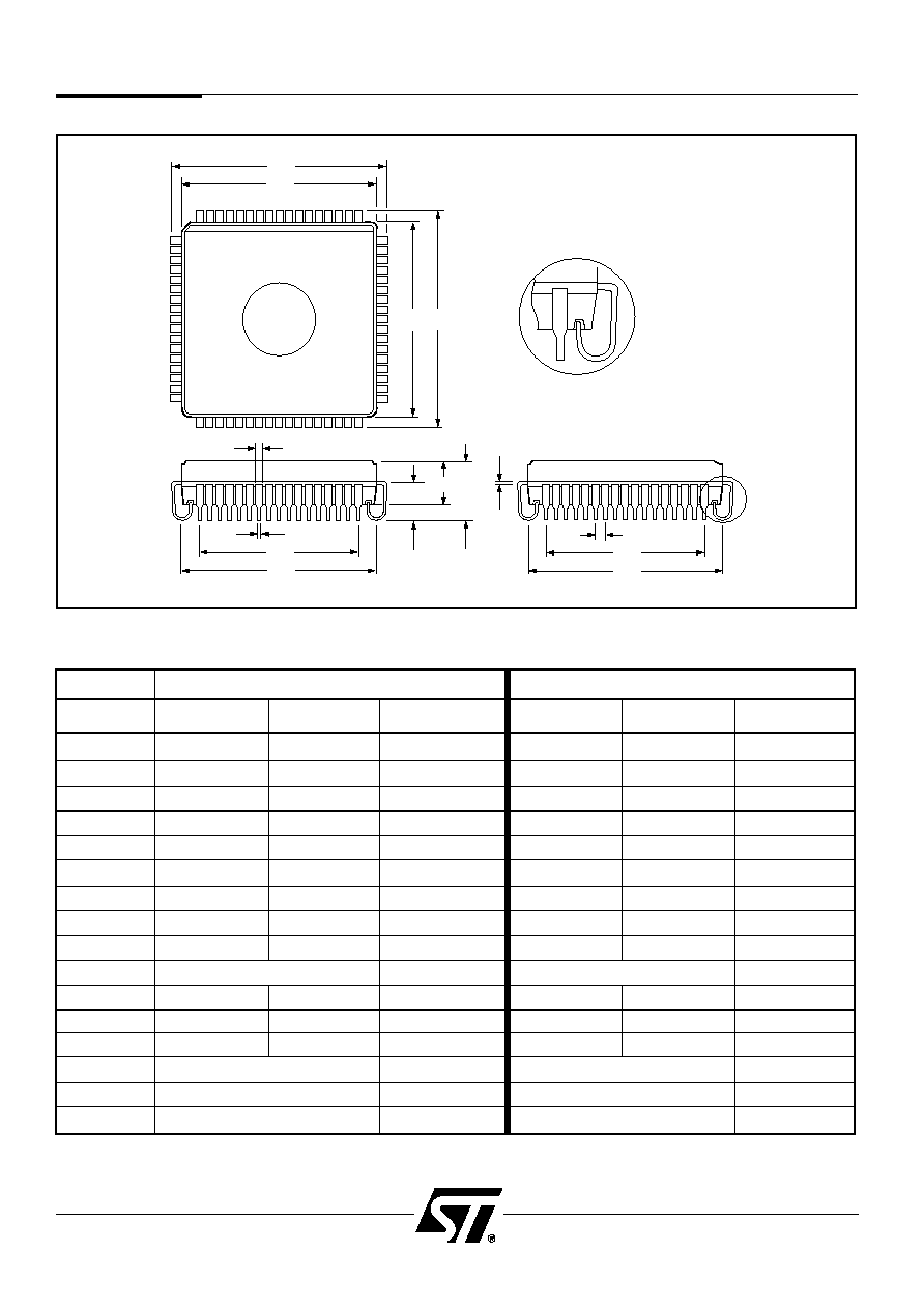
PSD5XX Family
140
Family: Ceramic Leaded Chip Carrier ≠ CERQUAD
Millimeters
Inches
Symbol
Min
Max
Notes
Min
Max
Notes
A
3.94
4.57
0.155
0.180
A1
2.29
2.92
0.090
0.115
A2
3.05
3.68
0.120
0.145
B
0.43
0.53
0.017
0.021
B1
0.66
0.81
0.026
0.032
C
0.15
0.25
0.006
0.010
D
25.02
25.27
0.985
0.995
D1
23.93
24.28
0.942
0.956
D2
22.35
23.88
0.880
0.940
D3
20.32
Reference
0.800
Reference
E
25.02
25.27
0.985
0.995
E1
23.93
24.28
0.942
0.956
E2
22.35
23.88
0.880
0.940
E3
20.32
Reference
0.800
Reference
e1
1.27
Reference
0.050
Reference
N
68
68
030195R6
Drawing L5 ≠ 68-Pin Pocketed Ceramic Leaded Chip Carrier (CLDCC) ≠ CERQUAD (Package Type L)
D3
B1
B
A1
A
E1
E
68
D2
A2
C
1
2
3
D1
D
E3
e1
To reduce lead damage,
lead tips reside in
pockets on the bottom
of the package.
View A
View A
E2
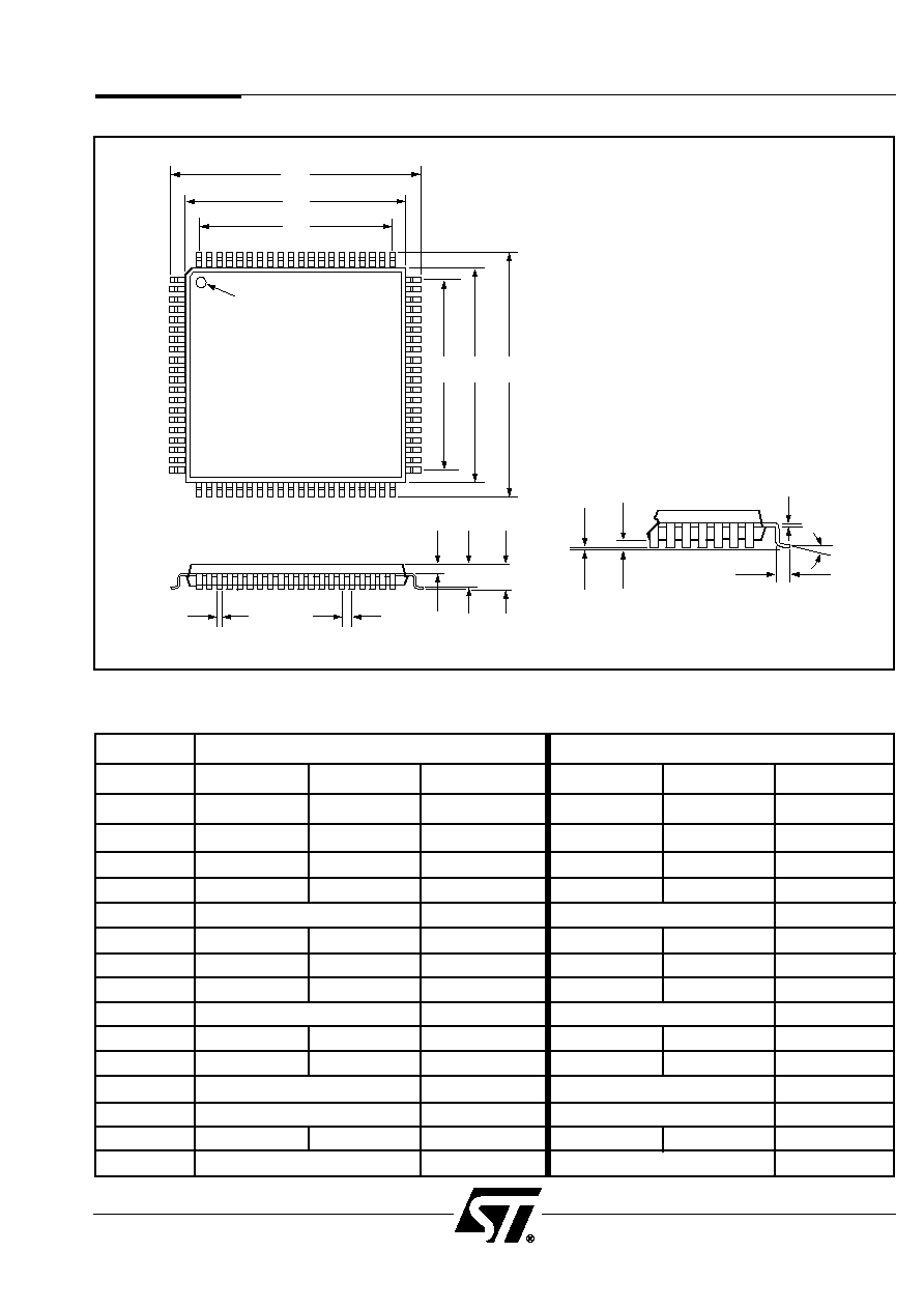
PSD5XX Family
141
Drawing U2 ≠ 80-Pin Plastic Thin Quad Flatpack (TQFP) (Package Type U)
D
D1
D3
E3
E1
E
Index
Mark
Standoff:
0.05 mm Min.
Load Coplanarity:
0.102 mm Max.
L
C
B
e1
A2
A
A1
80
1
2
3
Family: Plastic Thin Quad Flatpack (TQFP)
Millimeters
Inches
Symbol
Min
Max
Notes
Min
Max
Notes
0∞
8∞
0∞
8∞
A
≠
1.60
≠
0.063
A1
0.54
0.74
0.021
0.029
A2
1.15
1.55
0.045
0.061
B
0.30
Reference
0.012
Reference
C
0.09
0.20
0.004
0.008
D
15.75
16.25
0.620
0.640
D1
13.90
14.10
0.547
0.555
D3
12.35
Reference
0.486
Reference
E
15.75
16.25
0.620
0.640
E1
13.90
14.10
0.547
0.555
E3
12.35
Reference
0.486
Reference
e1
0.65
Reference
0.026
Reference
L
0.35
0.75
0.014
0.030
N
80
80
030195R1
PSD5XX Family
142
20.0
PSD5XX
Ordering
Information
Part #
MCU
PLDs/Decoders
I/O
Memory
Other
PSD
ZPSD
ZPSDV
Data Path
Inputs
Ports
EPROM
SRAM
Four 16-Bit Timer/Counters
Interface
Product Terms
(w/BB)
WatchDog (16-Bit)
Input Micro
Cells
Inter. Contr.
Output Micro
Cells
Periph. Mode
Outputs
Security
Page
APD
Reg.
PSD511B1 ZPSD511B1 ZPSD511B1V
8
PLUS2
61
140
24
24
X
40
256Kb
16Kb
X
X
X
X
X
X
PSD501B1 ZPSD501B1 ZPSD501B1V 16/8
PLUS2
61
140
24
24
X
40
256Kb
16Kb
X
X
X
X
X
X
ZPSD512B0
8
PSD512B1 ZPSD512B1 ZPSD512B1V
8
PLUS2
61
140
24
24
X
40
512Kb
16Kb
X
X
X
X
X
X
PSD502B1 ZPSD502B1 ZPSD502B1V 16/8
PLUS2
61
140
24
24
X
40
512Kb
16Kb
X
X
X
X
X
X
PSD513B1 ZPSD513B1 ZPSD513B1V
8
PLUS2
61
140
24
24
X
40
1024Kb
16Kb
X
X
X
X
X
X
PSD503B1 ZPSD503B1 ZPSD503B1V 16/8
PLUS2
61
140
24
24
X
40
1024Kb
16Kb
X
X
X
X
X
X
20.1 PSD5XX Family ≠ Selector Guide
PSD5XX Family
143
PSD5XX
Ordering
Information
Temperature (Blank = Commercial,
I = Industrial, M = Military)
Package Type
Speed (-70 = 70ns, -90 = 90ns, -15 = 150ns
-20 = 200ns, -25 = 250ns)
Revision (Blank = No Revision)
Supply Voltage (Blank = 5V, V = 3 Volt)
Base Part Number - see Selector Guide
PSD (WSI Programmable System Device) Fam.
Power Down Feature (Blank = Standard,
Z = Zero Power Feature)
Z
PSD
-A -20 J
I
413A2 V
Operating
Speed
Temperature
Part Number
(ns)
Package Type
Range
PSD501B1-C-70J
70
68 Pin PLDCC
Comm'l
PSD501B1-C-70L
70
68 Pin CLDCC
Comm'l
PSD501B1-C-70U
70
68 Pin TQFP
Comm'l
PSD501B1-C-90JI
90
68 Pin PLDCC
Industrial
PSD501B1-C-90UI
90
68 Pin TQFP
Industrial
PSD501B1-C-15J
150
68 Pin PLDCC
Comm'l
PSD501B1-C-15L
150
68 Pin CLDCC
Comm'l
PSD501B1-C-15U
150
68 Pin TQFP
Comm'l
PSD502B1-C-70J
70
68 Pin PLDCC
Comm'l
PSD502B1-C-70L
70
68 Pin CLDCC
Comm'l
PSD502B1-C-70U
70
68 Pin TQFP
Comm'l
PSD502B1-C-90JI
90
68 Pin PLDCC
Industrial
PSD502B1-C-90UI
90
68 Pin TQFP
Industrial
PSD502B1-C-15J
150
68 Pin PLDCC
Comm'l
PSD502B1-C-15L
150
68 Pin CLDCC
Comm'l
PSD502B1-C-15U
150
68 Pin TQFP
Comm'l
20.3 Ordering Information
20.2 Part Number Construction
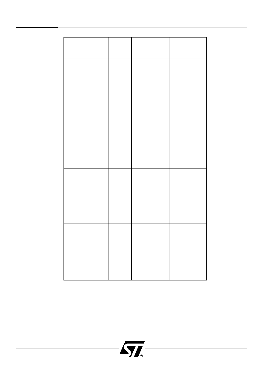
PSD5XX Family
144
Operating
Speed
Temperature
Part Number
(ns)
Package Type
Range
PSD503B1-C-70J
70
68 Pin PLDCC
Comm'l
PSD503B1-C-70L
70
68 Pin CLDCC
Comm'l
PSD503B1-C-70U
70
68 Pin TQFP
Comm'l
PSD503B1-C-90JI
90
68 Pin PLDCC
Industrial
PSD503B1-C-90UI
90
68 Pin TQFP
Industrial
PSD503B1-C-15J
150
68 Pin PLDCC
Comm'l
PSD503B1-C-15L
150
68 Pin CLDCC
Comm'l
PSD503B1-C-15U
150
68 Pin TQFP
Comm'l
PSD511B1-C-70J
70
68 Pin PLDCC
Comm'l
PSD511B1-C-70L
70
68 Pin CLDCC
Comm'l
PSD511B1-C-70U
70
68 Pin TQFP
Comm'l
PSD511B1-C-90JI
90
68 Pin PLDCC
Industrial
PSD511B1-C-90UI
90
68 Pin TQFP
Industrial
PSD511B1-C-15J
150
68 Pin PLDCC
Comm'l
PSD511B1-C-15L
150
68 Pin CLDCC
Comm'l
PSD511B1-C-15U
150
68 Pin TQFP
Comm'l
PSD512B1-C-70J
70
68 Pin PLDCC
Comm'l
PSD512B1-C-70L
70
68 Pin CLDCC
Comm'l
PSD512B1-C-70U
70
68 Pin TQFP
Comm'l
PSD512B1-C-90JI
90
68 Pin PLDCC
Industrial
PSD512B1-C-90UI
90
68 Pin TQFP
Industrial
PSD512B1-C-15J
150
68 Pin PLDCC
Comm'l
PSD512B1-C-15L
150
68 Pin CLDCC
Comm'l
PSD512B1-C-15U
150
68 Pin TQFP
Comm'l
PSD513B1-C-70J
70
68 Pin PLDCC
Comm'l
PSD513B1-C-70L
70
68 Pin CLDCC
Comm'l
PSD513B1-C-70U
70
68 Pin TQFP
Comm'l
PSD513B1-C-90JI
90
68 Pin PLDCC
Industrial
PSD513B1-C-90UI
90
68 Pin TQFP
Industrial
PSD513B1-C-15J
150
68 Pin PLDCC
Comm'l
PSD513B1-C-15L
150
68 Pin CLDCC
Comm'l
PSD513B1-C-15U
150
68 Pin TQFP
Comm'l
Ordering Information
PSD5XX
Ordering
Information
(cont.)
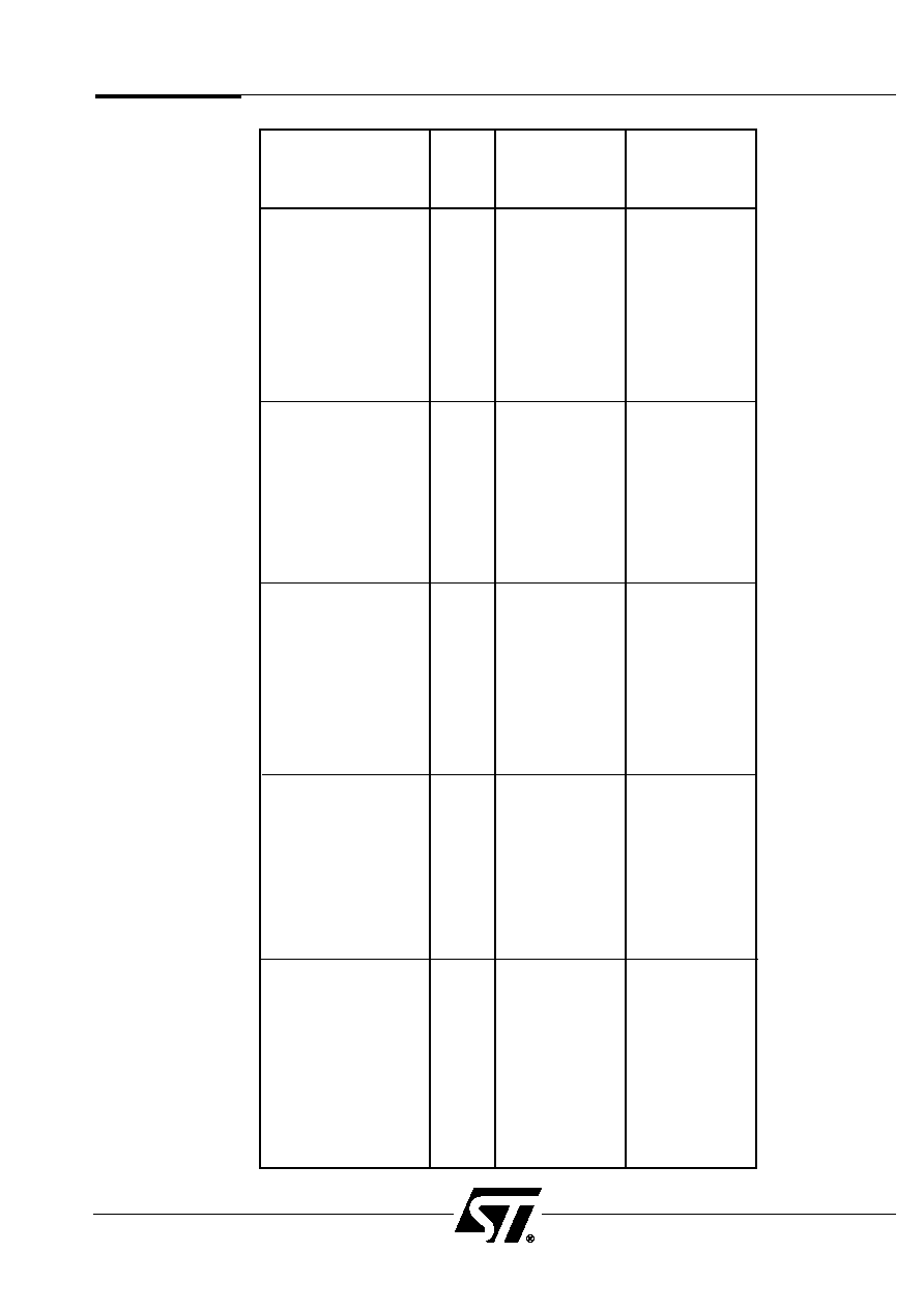
Operating
Speed
Temperature
Part Number
(ns)
Package Type
Range
ZPSD501B1-C-70J
70
68 Pin PLDCC
Comm'l
ZPSD501B1-C-70L
70
68 Pin CLDCC
Comm'l
ZPSD501B1-C-70U
70
80 Pin TQFP
Comm'l
ZPSD501B1-C-90JI
90
68 Pin PLDCC
Industrial
ZPSD501B1-C-90UI
90
80 Pin TQFP
Industrial
ZPSD501B1-C-15J
150
68 Pin PLDCC
Comm'l
ZPSD501B1-C-15L
150
68 Pin CLDCC
Comm'l
ZPSD501B1-C-15U
150
80 Pin TQFP
Comm'l
ZPSD501B1V-C-20J
200
68 Pin PLDCC
Comm'l
ZPSD501B1V-C-20JI
200
68 Pin PLDCC
Industrial
ZPSD501B1V-C-20L
200
68 Pin CLDCC
Comm'l
ZPSD501B1V-C-20U
200
80 Pin TQFP
Comm'l
ZPSD501B1V-C-20UI
200
80 Pin TQFP
Industrial
ZPSD501B1V-C-25J
250
68 Pin PLDCC
Comm'l
ZPSD501B1V-C-25L
250
68 Pin CLDCC
Comm'l
ZPSD501B1V-C-25U
250
80 Pin TQFP
Comm'l
ZPSD502B1-C-70J
70
68 Pin PLDCC
Comm'l
ZPSD502B1-C-70L
70
68 Pin CLDCC
Comm'l
ZPSD502B1-C-70U
70
80 Pin TQFP
Comm'l
ZPSD502B1-C-90JI
90
68 Pin PLDCC
Industrial
ZPSD502B1-C-90UI
90
80 Pin TQFP
Industrial
ZPSD502B1-C-15J
150
68 Pin PLDCC
Comm'l
ZPSD502B1-C-15L
150
68 Pin CLDCC
Comm'l
ZPSD502B1-C-15U
150
80 Pin TQFP
Comm'l
ZPSD502B1V-C-20J
200
68 Pin PLDCC
Comm'l
ZPSD502B1V-C-20JI
200
68 Pin PLDCC
Industrial
ZPSD502B1V-C-20L
200
68 Pin CLDCC
Comm'l
ZPSD502B1V-C-20U
200
80 Pin TQFP
Comm'l
ZPSD502B1V-C-20UI
200
80 Pin TQFP
Industrial
ZPSD502B1V-C-25J
250
68 Pin PLDCC
Comm'l
ZPSD502B1V-C-25L
250
68 Pin CLDCC
Comm'l
ZPSD502B1V-C-25U
250
80 Pin TQFP
Comm'l
ZPSD503B1-C-70J
70
68 Pin PLDCC
Comm'l
ZPSD503B1-C-70L
70
68 Pin CLDCC
Comm'l
ZPSD503B1-C-70U
70
80 Pin TQFP
Comm'l
ZPSD503B1-C-90JI
90
68 Pin PLDCC
Industrial
ZPSD503B1-C-90LI
90
68 Pin CLDCC
Industrial
ZPSD503B1-C-90UI
90
80 Pin TQFP
Industrial
ZPSD503B1-C-15J
150
68 Pin PLDCC
Comm'l
ZPSD503B1-C-15L
150
68 Pin CLDCC
Comm'l
ZPSD503B1-C-15U
150
80 Pin TQFP
Comm'l
PSD5XX Family
145
Ordering Information
PSD5XX
Product
Ordering
Information
(cont.)

PSD5XX Family
146
Operating
Speed
Temperature
Part Number
(ns)
Package Type
Range
ZPSD503B1V-C-20J
200
68 Pin PLDCC
Comm'l
ZPSD503B1V-C-20JI
200
68 Pin PLDCC
Industrial
ZPSD503B1V-C-20L
200
68 Pin CLDCC
Comm'l
ZPSD503B1V-C-20U
200
80 Pin TQFP
Comm'l
ZPSD503B1V-C-20UI
200
80 Pin TQFP
Industrial
ZPSD503B1V-C-25J
250
68 Pin PLDCC
Comm'l
ZPSD503B1V-C-25L
250
68 Pin CLDCC
Comm'l
ZPSD503B1V-C-25U
250
80 Pin TQFP
Comm'l
ZPSD511B1-C-70J
70
68 Pin PLDCC
Comm'l
ZPSD511B1-C-70L
70
68 Pin CLDCC
Comm'l
ZPSD511B1-C-70U
70
80 Pin TQFP
Comm'l
ZPSD511B1-C-90JI
90
68 Pin PLDCC
Industrial
ZPSD511B1-C-90UI
90
80 Pin TQFP
Industrial
ZPSD511B1-C-15J
150
68 Pin PLDCC
Comm'l
ZPSD511B1-C-15L
150
68 Pin CLDCC
Comm'l
ZPSD511B1-C-15U
150
80 Pin TQFP
Comm'l
ZPSD511B1V-C-20J
200
68 Pin PLDCC
Comm'l
ZPSD511B1V-C-20JI
200
68 Pin PLDCC
Industrial
ZPSD511B1V-C-20L
200
68 Pin CLDCC
Comm'l
ZPSD511B1V-C-20U
200
80 Pin TQFP
Comm'l
ZPSD511B1V-C-20UI
200
80 Pin TQFP
Industrial
ZPSD511B1V-C-25J
250
68 Pin PLDCC
Comm'l
ZPSD511B1V-C-25L
250
68 Pin CLDCC
Comm'l
ZPSD511B1V-C-25U
250
80 Pin TQFP
Comm'l
ZPSD512B0-C-70J
70
68 Pin PLDCC
Comm'l
ZPSD512B0-C-70L
70
68 Pin CLDCC
Comm'l
ZPSD512B0-C-70U
70
80 Pin TQFP
Comm'l
ZPSD512B0-C-90JI
90
68 Pin PLDCC
Industrial
ZPSD512B0-C-90UI
90
80 Pin TQFP
Industrial
ZPSD512B0-C-15J
150
68 Pin PLDCC
Comm'l
ZPSD512B0-C-15L
150
68 Pin CLDCC
Comm'l
ZPSD512B0-C-15U
150
80 Pin TQFP
Comm'l
ZPSD512B1-C-70J
70
68 Pin PLDCC
Comm'l
ZPSD512B1-C-70L
70
68 Pin CLDCC
Comm'l
ZPSD512B1-C-70U
70
80 Pin TQFP
Comm'l
ZPSD512B1-C-90JI
90
68 Pin PLDCC
Industrial
ZPSD512B1-C-90UI
90
80 Pin TQFP
Industrial
ZPSD512B1-C-15J
150
68 Pin PLDCC
Comm'l
ZPSD512B1-C-15L
150
68 Pin CLDCC
Comm'l
ZPSD512B1-C-15U
150
80 Pin TQFP
Comm'l
Ordering Information
PSD5XX
Product
Ordering
Information
(cont.)
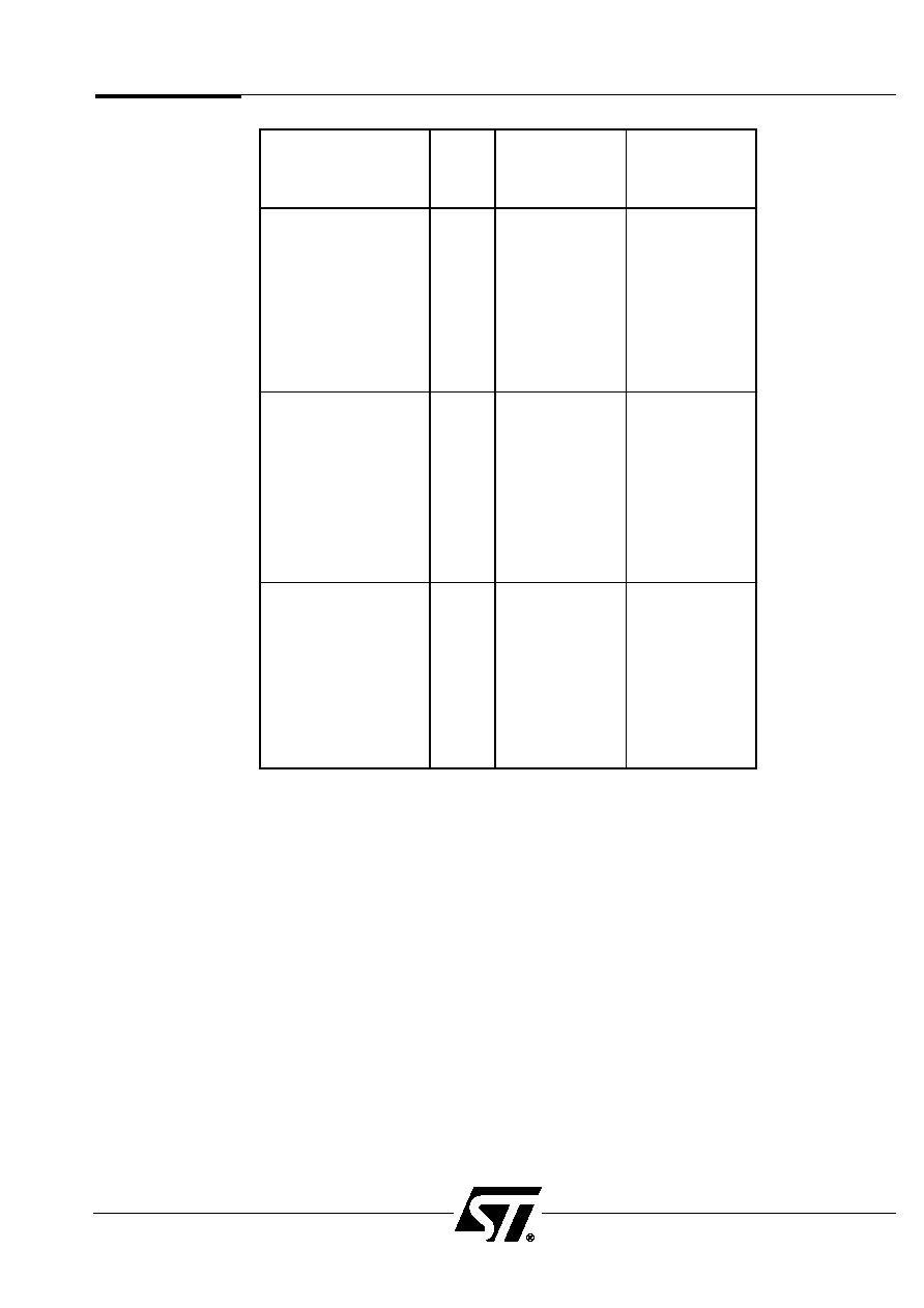
PSD5XX Family
147
Operating
Speed
Temperature
Part Number
(ns)
Package Type
Range
ZPSD512B1V-C-20J
200
68 Pin PLDCC
Comm'l
ZPSD512B1V-C-20JI
200
68 Pin PLDCC
Industrial
ZPSD512B1V-C-20L
200
68 Pin CLDCC
Comm'l
ZPSD512B1V-C-20U
200
80 Pin TQFP
Comm'l
ZPSD512B1V-C-20UI
200
80 Pin TQFP
Industrial
ZPSD512B1V-C-25J
250
68 Pin PLDCC
Comm'l
ZPSD512B1V-C-25L
250
68 Pin CLDCC
Comm'l
ZPSD512B1V-C-25U
250
80 Pin TQFP
Comm'l
ZPSD513B1-C-70J
70
68 Pin PLDCC
Comm'l
ZPSD513B1-C-70L
70
68 Pin CLDCC
Comm'l
ZPSD513B1-C-70U
70
80 Pin TQFP
Comm'l
ZPSD513B1-C-90JI
90
68 Pin PLDCC
Industrial
ZPSD513B1-C-90UI
90
80 Pin TQFP
Industrial
ZPSD513B1-C-15J
150
68 Pin PLDCC
Comm'l
ZPSD513B1-C-15L
150
68 Pin CLDCC
Comm'l
ZPSD513B1-C-15U
150
80 Pin TQFP
Comm'l
ZPSD513B1V-C-20J
200
68 Pin PLDCC
Comm'l
ZPSD513B1V-C-20JI
200
68 Pin PLDCC
Industrial
ZPSD513B1V-C-20L
200
68 Pin CLDCC
Comm'l
ZPSD513B1V-C-20U
200
80 Pin TQFP
Comm'l
ZPSD513B1V-C-20UI
200
80 Pin TQFP
Industrial
ZPSD513B1V-C-25J
250
68 Pin PLDCC
Comm'l
ZPSD513B1V-C-25L
250
68 Pin CLDCC
Comm'l
ZPSD513B1V-C-25U
250
80 Pin TQFP
Comm'l
Ordering Information
PSD5XX
Product
Ordering
Information
(cont.)

PSD5XX Family
148
21.0
Process
Change Notice,
October 1, 1998
PSD5XX Functional Change:
A change has been implemented in the most recent silicon that improves the way that the
Image Register is updated. This change only applies to Event Count Mode for counter units
CTU0, CTU1, and CTU3.
Previous PSD5XX Silicon:
The Image Register was not updated with the actual event count upon exiting Freeze
mode. As a result, in certain circumstances, the Image Register may not have reflected the
actual event count. Although an incorrect count may have been read from the Image
Register at a given time, no event counts were ever lost because the microcontroller would
eventually read the correct value in the Image Register on subsequent freeze and read
cycles.
Current PSD5XX Silicon:
The Image register is now automatically updated with the actual count upon exiting the
Freeze mode. This ensures that on the very next freeze and read cycle, the microcontroller
will read the actual count from the Image register. There are two restrictions however:
1. If an event occurs within one timer clock period plus two CLKIN periods after the image
register is unfrozen, then the Image Register will not reflect that event on the very next
freeze and read cycle (timer clock period is defined on page 6-79 of the 1996 PSD data
book). Instead, the event will appear in the Image Register on the subsequent freeze
and read cycle.
2. The time between an unfreeze and the beginning of the next freeze has the same time
constraint as number one. There must be at least one timer clock period plus two CLKIN
periods between the end of one freeze cycle and the beginning of the next. This timing
can be controlled by software design.
To reduce the chance of getting a delayed count in the Image Register due to restriction
number 1, execute a software Load/Store command just prior to freezing and reading the
Image Register to force an update to the Image count.
Backwards Compatibility:
This improvement should have no impact on current designs unless these designs
were compensating for lost events. In such cases, compatibility is dependent on the
compensation method that was used. Please contact WSI at apphelp@wsiusa.com if you
think you have an issue or have any questions.
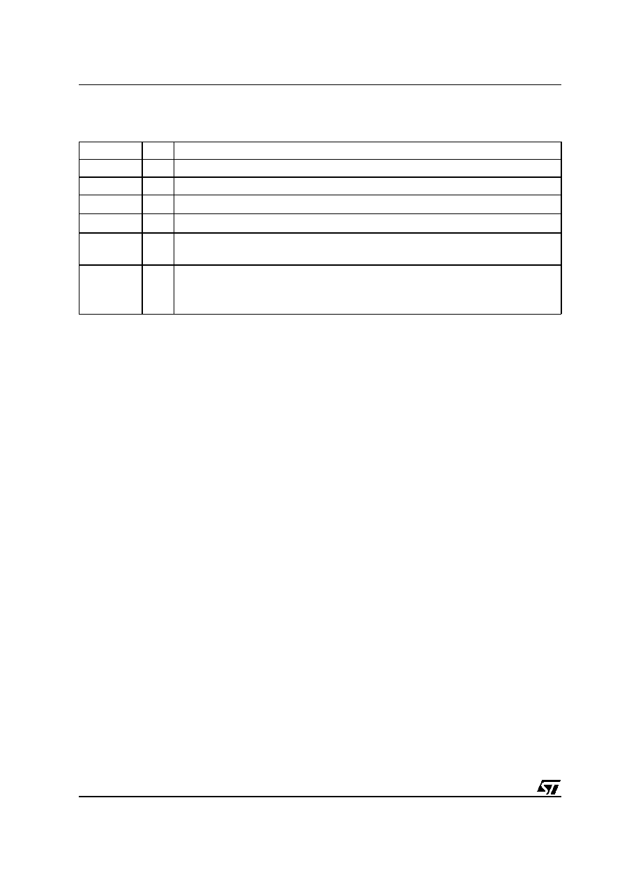
PSD5XX, ZPSD5XX
2/3
REVISION HISTORY
Table 1. Document Revision History
Date
Rev.
Description of Revision
Apr-1994
1.0
PSD5XX: Document written in the WSI format. Initial release
Jun-1995
1.1
ZPSD5XX: Updated Specifications
Mar-1997
1.2
ZPSD5XX Updated specifications
May-1998
1.3
PSD5XX, ZPSD5XX Updated specifications, various speed grades removed
Feb-1999
1.4
PSD5XX, ZPSD5XX Combined Data Sheets, eliminated military parts, eliminated various
speed grades, updated specifications.
31-Jan-2002
1.5
PSD5XX, ZPSD5XX: Low Cost Field Programmable Microcontroller Peripherals
Front page, and back two pages, in ST format, added to the PDF file
Any references to Waferscale, WSI, EasyFLASH and PSDsoft 2000
updated to ST, ST, Flash+PSD and PSDsoft Express

3/3
PSD5XX, ZPSD5XX
Information furnished is believed to be accurate and reliable. However, STMicroelectronics assumes no responsibility for the consequences
of use of such information nor for any infringement of patents or other rights of third parties which may result from its use. No license is granted
by implication or otherwise under any patent or patent rights of STMicroelectronics. Specifications mentioned in this publication are subject
to change without notice. This publication supersedes and replaces all information previously supplied. STMicroelectronics products are not
authorized for use as critical components in life support devices or systems without express written approval of STMicroelectronics.
The ST logo is registered trademark of STMicroelectronics
All other names are the property of their respective owners
© 2002 STMicroelectronics - All Rights Reserved
STMicroelectronics group of companies Australia - Brazil - Canada - China - Finland - France - Germany - Hong Kong -
India - Israel - Italy - Japan - Malaysia - Malta - Morocco - Singapore - Spain - Sweden - Switzerland - United Kingdom - United States.
www.st.com