 | –≠–Ľ–Ķ–ļ—ā—Ä–ĺ–Ĺ–Ĺ—č–Ļ –ļ–ĺ–ľ–Ņ–ĺ–Ĺ–Ķ–Ĺ—ā: S9418P | –°–ļ–į—á–į—ā—Ć:  PDF PDF  ZIP ZIP |
SUMMIT MICROELECTRONICS, Inc. ∑ 300 Orchard City Drive, Suite 131 ∑ Campbell, CA 95008 ∑ Telephone 408-378-6461 ∑ Fax 408-378-6586 ∑ www.summitmicro.com
1
© SUMMIT MICROELECTRONICS, Inc. 2000
2023 2.2 8/2/00
Characteristics subject to change without notice
SUMMIT
MICROELECTRONICS, Inc.
FEATURES
∑
Four 8-Bit DACs
-- Differential Non-linearity: Ī0.5LSB max
-- Integral Non-Linearity Error: Ī1LSB max
∑
Each DAC has Independent Reference Inputs
-- Output Buffer Amplifiers Swing Rail-to-Rail
-- Ground to V
DD
Reference Input Range
∑ Each DAC's Digital Inputs Maintained in
EEPROM
∑ Power-On Reset Reloads Registers with Non-
volatile Data
∑ Simple Serial Interface for Reading and Writing
DAC values, SPITM and QSPITM compatible.
∑
Fully operational from 2.7V to 5.5V
∑
Low Power, 4mW max at +5V
Quad 8-Bit Nonvolatile DACPOTTM Electronic Potentiometer
With a Mute Control Input
S9418
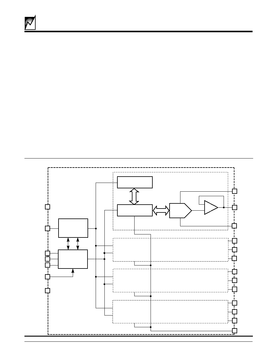
OVERVIEW
The S9418 DACPOTTM is a serial input, voltage output,
quad 8-bit digital to analog converter (DAC). The S9418
operates from a single 2.7V to 5.5V supply. Internal
precision buffers swing rail-to-rail and the reference input
range includes both ground and the positive supply.
The S9418 integrates four 8-bit DACs and their associ-
ated circuits which include; an enhanced unity gain opera-
tional amplifier output, an 8-bit data latch, an 8-bit non-
volatile register and an industry standard serial interface
for reading and writing data to the DACs' data latches and
registers. The DACs are independently programmable
and each has its own electrically isolated Vreference
inputs.
BLOCK DIAGRAM
VREFH0
VOUT0
18
2
8-Bit E2PROM
8-Bit Data Register
Serial
Data In
Serial Data Out
8-Bit DAC
AMP
VDD
3
RDY/BSY#
4
VREFL0
9
11
CS#
DI
7
6
MUTE
CLK
5
VREFH1
VOUT1
17
1
VREFL1
12
VREFH2
VOUT2
16
20
VREFL2
13
VREFH3
VOUT3
15
19
VREFL3
14
DAC SECTION 0
DAC SECTION 1
DAC SECTION 2
DAC SECTION 3
DO
8
Memory Control
Programming
Memory
Controller
Control
Logic
GND
10
2
S9418
2023 2.2 8/2/00
The analog outputs of the S9418 can be programmed to
any one of 256 individual voltage steps. Each step value
is 1/256
th
of the voltage differential between V
REFH
and
V
REFL
of the respective DAC. Once programmed these
settings can be retained in nonvolatile memory during all
power conditions and will be automatically recalled upon
a power-up sequence. Each DAC can be independently
read without affecting the output voltage during the read
cycle. In addition each output can be adjusted an unlim-
ited number of times without altering the value stored in
the nonvolatile memory.
DEVICE OPERATION
Analog Section
The S9418 is an 8-bit, voltage output digital-to-analog
converter (DAC). The DAC consists of a resistor network
that converts 8-bit digital inputs into equivalent analog
output voltages in proportion to the applied reference
voltage.
Reference inputs
The voltage differential between the V
REFL
and V
REFH
inputs sets the full-scale output voltage for its respective
DAC. V
REFL
must be equal to or greater than ground
(positive voltage). V
REFH
must be greater (more positive)
than V
REFL
or equal to V
DD
.
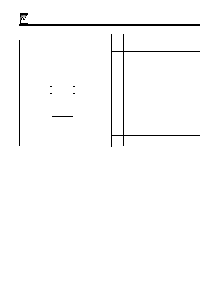
PINOUT and SIGNAL DEFINITION
Pin
Name
Function
1, 2
V
REFH
Vreference High:
19, 20
V
REFH
- V
DD
> V
REFL
3
V
DD
Power Supply Voltage
4
RDY/
Ready/Busy#: open drain output
BSY#
indicating status of nonvolatile
write operations
5
CLK
Clock Input Pin: used for serial
data communication
6
CS#
Chip Select: When high deselects
the device and places it in a low
power mode
7
DI
Data Input: serial data input pin
8
DO
Data Output: serial data output pin
9
MUTE
When active forces V
OUT
to V
REFL
10
GND
Power Supply Ground
11, 12
V
REFL
Vreference Low
13, 14
15, 16
V
OUT
DAC Output: buffered D to A
17, 18
converter output
Output Buffer Amplifiers
The voltage outputs are from precision unity-gain follow-
ers that can slew up to 1V/Ķs. The outputs can swing from
V
REFL
to V
REFH
. With a 0V to 5V output transition the
amplifier outputs typically settle to 1LSB in 40Ķs.
DIGITAL INTERFACE
The S9418 employs a common 4-wire serial interface. It
is comprised of a Clock (CLK), Chip Select (CS#), Data
input (DI) and Data output (DO). Data is clocked into the
device on the clock's rising edge and out of the device on
the clock's falling edge. Data is shifted in and out MSB first.
DO only becomes active after the device has been se-
lected and after a valid read command and address has
been received.
All data transfers are initiated after CS# goes low and a
logic `1' is clocked into the device. This first data transfer
is the start bit and must precede all operations. Following
the start bit are two command bits used to specify which
of four commands to execute. The next two bits are the
address bits used to select one of the four DACs. The
action of the next eight clock cycles will be dependent
upon the command issued.
VREFH1
VREFH0
VDD
RDY/BSY#
CLK
CS#
DI
DO
MUTE
GND
VREFH2
VREFH3
VOUT0
VOUT1
VOUT2
VOUT3
VREFL3
VREFL2
VREFL1
VREFL0
1
2
3
4
5
6
7
8
9
10
20
19
18
17
16
15
14
13
12
11
2023 T PCon 2.0
20-Pin PDIP
or 20-Pin SOIC
S9418
3
2023 2.2 8/2/00
Internally there are four DACs and associated with each
are two registers. There is one data register that is used
by the DAC to hold the digital value it converts. There is
also one nonvolatile register that holds the default value
that can be recalled into the data register during power-
up or by executing the Recall command.
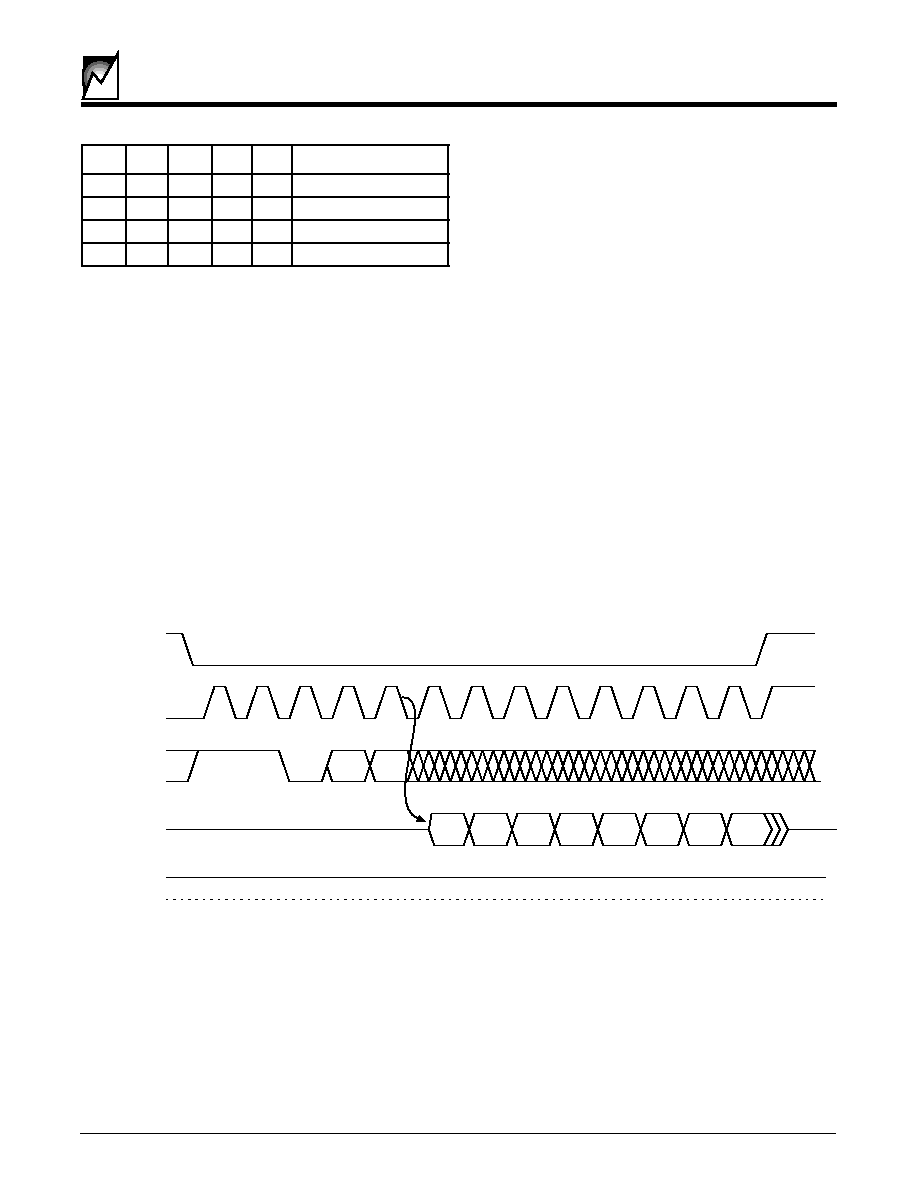
READ
Read operations are initiated by taking CS# low and
clocking in a start bit followed by the read command and
the address of the data register to be read. The next eight
clocks will output on the DO pin the contents of the
selected data register. This read will not affect the contents
of the register or the output of the DAC. Refer to Figure 1
for an illustration of the sequence of bus conditions for a
read operation.
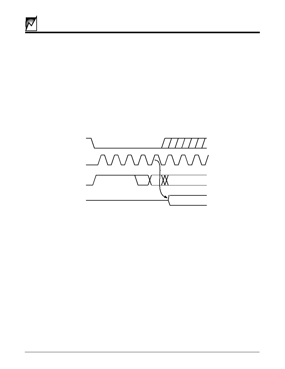
WRITE
Write operations are initiated by taking CS# low and
clocking in a start bit followed by the write command and
the address of the data register to be written. This action
is followed by the host clocking eight bits of data into the
register, MSB first. The output of the selected DAC will
change as the last bit is clocked into the device. At this
point the clock counter will reset the command register,
requiring a full sequence to be initiated in order to write to
the DAC again.
Refer to Figure 2 for an illustration of the
sequence of bus conditions for a write operation.
NOTE: This write operation does not affect the contents of
the nonvolatile register. Therefore, the nonvolatile register
can contain the power-on default settings (e.g. volume),
and the write DAC command can be used to make
situational adjustments.
FIGURE 1. READ SEQUENCE
TABLE 1.
t
r
a
t
S
C
1
C
0
A
1
A
0
d
n
a
m
m
o
C
1
0
0
A
A
e
l
b
a
n
E
e
t
i
r
W
V
N
1
0
1
A
A
n
I
a
t
a
D
--
e
t
i
r
W
1
1
0
A
A
t
u
O
a
t
a
D
--
d
a
e
R
1
1
1
A
A
ll
a
c
e
R
S
T
A
R
T
C
A
C
A
1
1
0
0
CLK
DI
DO
Hi Z
D
D
1
0
3
4
5
6
7
2
D
D
D
D
D
D
Hi Z
2023 T fig01 2.0
RDY/BSY#
CS#
(Pulled up to V
DD
)

4
S9418
2023 2.2 8/2/00
FIGURE 2. WRITE SEQUENCE
NONVOLATILE WRITE
A nonvolatile write is a two step operation: it is initiated by
taking CS# low and clocking in a start bit followed by the
NV Write Enable command. At this point the host can take
CS# back high or continue clocking in data. This data is
don't care and will be ignored by the S9418.
Next, the host takes CS# low again and issues a write
command and address and then clocks in the eight data
bits to be programmed. The host will then bring CS# high
and the data will be latched into the data register and a
nonvolatile write operation will commence.
FIGURE 3. NONVOLATILE WRITE SEQUENCE
The status of the nonvolatile write can be monitored on the
RDY/BSY# pin. A logic low indicates the write is still in
progress and the S9418 will not be accessible to the host;
a logic high indicates the write has completed and the
S9418 is ready for the next command. Refer to Figure 3
for an illustration of the sequence of bus conditions for a
nonvolatile write operation.
e
S
T
A
R
T
C
D
A
C
D
A
1
0
3
4
5
6
7
1
1
2
0
0
D
D
D
D
D
D
CLK
DI
DO
Hi Z
VOUT
2023 T fig02 2.0
CS#
RDY/BSY#
(Pulled up to V
DD
)
A
0
1
D
CLK
DI
Rising Edge Sets
NV Write Enable Latch
C
C
1
0
C
C
1
0
D
A
D
A
1
0
3
4
5
6
7
1
2
0
D
D
D
D
D
D
Address and Data
are Don't Care
Rising Edge Starts
NV Write
NV Write Enable
Latch is Reset
2023 T fig03 2.0
CS#
RDY/BSY#
S9418
5
2023 2.2 8/2/00
FIGURE 4. RECALL COMMAND SEQUENCE
RECALL COMMAND
The recall command will retrieve data from the selected
nonvolatile register and write it into the data register of the
associated DAC. This operation is initiated by taking CS#
low and clocking in a start bit followed by the recall
command and the address of the nonvolatile register to be
recalled. The eight bits of data are don't care, so CS# can
be taken high any time after the address bits are clocked
in. Refer to Figure 4 for an illustration of the sequence of
bus conditions for a Recall operation.
Power-On Recall
Whenever the S9418 is powered on, the V
OUT
values will
be returned to the analog equivalent of the data byte stored
in the nonvolatile register.
MUTE Operation
The MUTE input is active high. Whenever the input is low
the V
OUT
will reflect the value in the data register. If MUTE
is driven high the V
OUT
outputs will be switched to V
REFL
.
Releasing the MUTE input returns the V
OUT
outputs to the
analog equivalent of the data register contents.
S
T
A
R
T
C
A
C
A
1
1
0
0
CLK
DI
V
OUT
2023 T fig04 2.0
CS#
6
S9418
2023 2.2 8/2/00
ABSOLUTE MAXIMUM RATINGS
VDD to GND .................................................................... -0.5V to +7V
Digital Inputs to Gnd ............................................. -0.5V to VDD+0.5V
Analog Inputs to ground ....................................... -0.5V to VDD+0.5V
Digital Outputs to Gnd .......................................... -0.5V to VDD+0.5V
Analog Outputs to Gnd ......................................... -0.5V to VDD+0.5V
Temperature Under Bias ........................................... -55įC to +125įC
Storage Temperature ................................................ -65įC to +150įC
Lead Soldering (10 Sec Max) .................................................... 300įC
Stresses listed under Absolute Maximum Ratings may cause perma-
nent damage to the device. These are stress ratings only, and functional
operation of the device at these or any other conditions outside those
listed in the operational sections of this specification is not implied.
Exposure to any absolute maximum rating for extended periods may
affect device performance and reliability.
DC ELECTRICAL CHARACTERISTICS (over recommended operating conditions unless otherwise specified)
Condition
Min
Max
Temperature
-40įC
+85įC
V
DD
+2.7V
+5.5V
RECOMMENDED OPERATING CONDITIONS
2023 PGM T2 1.1
RELIABILITY CHARACTERISTICS (over recommended operating conditions unless otherwise specified)
l
o
b
m
y
S
r
e
t
e
m
a
r
a
P
n
i
M
x
a
M
t
i
n
U
V
P
A
Z
y
t
il
i
b
i
t
p
e
c
s
u
S
D
S
E
0
0
0
2
V
I
H
T
L
p
u
-
h
c
t
a
L
0
0
1
A
m
T
R
D
n
o
i
t
n
e
t
e
R
a
t
a
D
0
0
1
s
r
a
e
Y
N
D
N
E
e
c
n
a
r
u
d
n
E
0
0
0
,
0
0
0
,
1
s
e
l
c
y
C
e
g
a
r
o
t
S
l
o
b
m
y
S
r
e
t
e
m
a
r
a
P
s
n
o
i
t
i
d
n
o
C
n
i
M
p
y
T
x
a
M
t
i
n
U
I
D
D
e
r
o
t
s
g
n
i
r
u
d
t
n
e
r
r
u
c
y
l
p
p
u
S
)
1
e
t
o
n
(
V
=
S
C
L
I
8
.
1
5
.
2
A
m
I
B
S
t
n
e
r
r
u
c
y
l
p
p
u
s
y
b
d
n
a
t
S
V
=
S
C
H
I
0
6
2
0
0
5
A
Ķ
I
H
I
t
n
e
r
r
u
c
e
g
a
k
a
e
l
t
u
p
n
I
V
N
I
V
=
D
D
1
<
0
1
A
Ķ
I
L
I
t
n
e
r
r
u
c
e
g
a
k
a
e
l
t
u
p
n
I
V
N
I
V
0
=
1
<
0
1
≠
A
Ķ
V
H
I
e
g
a
t
l
o
v
t
u
p
n
i
l
e
v
e
l
h
g
i
H
V
5
.
4
C
C
V
V
5
.
5
2
V
D
D
V
C
C
V
V
5
.
4
9
.
0
◊
V
C
C
V
D
D
V
V
L
I
e
g
a
t
l
o
v
t
u
p
n
i
l
e
v
e
l
w
o
L
V
5
.
4
C
C
V
V
5
.
5
0
8
.
0
V
C
C
V
V
5
.
4
0
1
.
0
◊
V
C
C
V
V
H
O
e
g
a
t
l
o
v
t
u
p
t
u
o
l
e
v
e
l
h
g
i
H
A
Ķ
0
0
4
≠
=
H
O
I
V
D
D
3
.
0
≠
V
V
L
O
e
g
a
t
l
o
v
t
u
p
t
u
o
l
e
v
e
l
w
o
L
,
A
m
1
=
L
O
I
V
D
D
;
V
5
=
,
A
m
4
.
0
=
L
O
I
V
D
D
V
7
.
2
=
4
.
0
V
Note 1: I
DD
is the supply current drawn while the EEPROM is being updated.
Typical T
A
= 25ļC and V
CC
= 5.0V.
3.0
S9418
7
2023 2.2 8/2/00
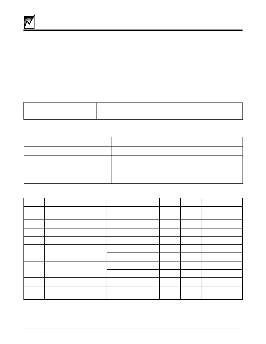
FIGURE 5. AC TIMING DIAGRAM
Symbol
Parameter
Conditions
Min.
Typ.
Max.
Units
fC
Clock Frequency
DC
1
MHz
tWH
Minimum CLK High Time
500
ns
tWL
Minimum CLK Low Time
300
ns
tCS
Minimum CS High Time
150
ns
tCSS
CS Setup Time
100
ns
tCSH
CS Hold Time
0
ns
tSU
Data In Setup Time
CL = 100pF
50
ns
tH
Data In Hold Time
See Note 1
50
ns
tV
Output Valid Time
150
ns
tHO
Data Out Hold Time
0
ns
tDIS
Output Disable Time
400
ns
tBUSY
Write Cycle Time
3.3
5
ms
Notes: 1. All timing measurements are defined at the point of signal crossing V
DD
/2.
AC ELECTRICAL CHARACTERISTICS
V
DD
= +4.5V to +5.5V, V
REFH
= V
DD
, V
REFL
= 0V, T
A
= -40įC to +85įC, unless otherwise specified
2023 PGM T5 1.1
t
HO
t
DIS
t
CS
t
WH
Hi Z
Hi Z
t
SU
t
H
t
CSS
t
WL
t
V
CLK
DI
DO
t
CSH
2023 T fig05 2.0
RDY/BSY#
CS#

8
S9418
2023 2.2 8/2/00
DAC ELECTRICAL CHARACTERISTICS
V
DD
= 2.7V to 5.5V, V
REFH
= VDD, V
REFL
= 0V, T
A
= ≠40ļC to 85ļC, unless otherwise specified
y
t
r
e
p
o
r
P
l
o
b
m
y
S
r
e
t
e
m
a
r
a
P
s
n
o
i
t
i
d
n
o
C
n
i
M
p
y
T
x
a
M
t
i
n
U
y
c
a
r
u
c
c
A
L
N
I
y
t
i
r
a
e
n
il
-
n
o
n
l
a
r
g
e
t
n
I
I
D
A
O
L
A
Ķ
0
0
1
=
5
.
0
1
Ī
B
S
L
L
N
D
y
t
i
r
a
e
n
il
-
n
o
n
l
a
i
t
n
e
r
e
f
f
i
D
I
D
A
O
L
)
1
e
t
o
n
(
A
Ķ
0
0
1
=
1
.
0
5
.
0
Ī
B
S
L
s
e
c
n
e
r
e
f
e
R
V
H
F
E
R
e
g
a
t
l
o
v
t
u
p
n
I
V
L
F
E
R
V
V
L
F
E
R
e
g
a
t
l
o
v
t
u
p
n
I
D
N
G
V
R
N
I
V
H
F
E
R
V
o
t
L
F
E
R
e
c
n
a
t
s
i
s
e
r
k
0
4
R
C
T
N
I
R
f
o
t
n
e
i
c
i
f
f
e
o
c
.
p
m
e
T
N
I
0
0
3
0
0
6
C
ļ
/
m
p
p
R
N
I
h
c
t
a
m
e
c
n
a
t
s
i
s
e
r
t
u
p
n
I
5
.
0
Ī
1
Ī
%
g
o
l
a
n
A
t
u
p
t
u
O
G
S
F
E
r
o
r
r
e
n
i
a
g
e
l
a
c
s
-
ll
u
F
F
F
=
D
X
E
H
1
Ī
B
S
L
V
T
U
O
S
Z
e
g
a
t
l
o
v
t
e
s
f
f
o
t
u
p
t
u
O
0
0
=
D
X
E
H
0
5
.
2
5
V
m
V
C
T
T
U
O
V
T
U
O
t
n
e
i
c
e
i
f
f
e
o
c
.
p
m
e
t
V
D
D
I
,
V
5
=
D
A
O
L
A
Ķ
0
5
=
)
1
e
t
o
n
(
0
5
C
ļ
/
V
Ķ
I
L
t
n
e
r
r
u
c
d
a
o
l
t
u
p
t
u
o
p
m
A
0
0
2
≠
0
0
0
1
A
Ķ
R
T
U
O
e
c
n
a
t
s
i
s
e
r
t
u
p
t
u
o
p
m
A
V
D
D
V
=
H
F
E
R
V
5
V
3
0
1
0
2
R
R
S
P
n
o
i
t
c
e
j
e
r
y
l
p
p
u
s
r
e
w
o
P
I
D
A
O
L
A
Ķ
0
1
=
1
V
/
B
S
L
t
S
B
S
L
1
o
t
e
m
i
t
g
n
il
t
t
e
s
C
A
D
F
p
0
1
V
5
V
3
F
p
0
1
6
3
7
2
0
4
5
3
s
Ķ
s
Ķ
e
N
e
s
i
o
n
t
u
p
t
u
o
p
m
A
V
,
z
H
k
1
=
f
D
D
V
5
=
0
9
V
n
z
H
D
H
T
n
o
i
t
r
o
t
s
i
d
c
i
n
o
m
r
a
h
l
a
t
o
T
V
H
F
E
R
V
,
V
5
.
2
=
D
D
,
V
5
=
V
,
z
H
k
1
=
f
N
I
V
1
=
S
M
R
8
0
.
0
%
W
B
B
d
3
≠
h
t
d
i
w
d
n
a
B
V
H
F
E
R
V
,
V
5
.
2
=
D
D
,
V
5
=
V
N
I
V
m
0
0
1
=
S
M
R
0
0
3
z
H
k
Note 1: Guaranteed but not tested.
Typical T
A
= 25ļC and V
CC
= 5.0V.
S9418
9
2023 2.2 8/2/00
20 Pin SOIC (.300) Package
0.014 - 0.019
(0.356 - 0.482)
0.004 - 0.012
(0.102 - 0.305)
0.037 - 0.045
(0.940 - 1.143
0.496 - 0.512
(12.598 - 13.005)
0.394 - 0.419
(10.007 - 10.643)
0.093 - 0.104
(2.362 - 2.642)
0.016 - 0.050
(0.406 - 1.270)
0.050
(1.270)
0.009 - 0.013
(0.229 - 0.330)
0.010 - 0.029
(0.254 - 0.737)
0.291 - 0.299
(7.391 - 7.595)
20pn SOIC ILL.1
0
į
to 8
į
typ
x45
į
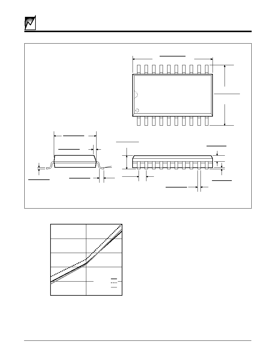
FIGURE 6. V
L
TO V
H
END-TO-END RESISTANCE OVER
TEMPERATURE
41.5
41.0
40.5
40.0
39.5
39.0
RESIST
ANCE (k
)
TEMPERATURE (ļC)
≠40
90
25
VL = GND
VH = 5.5V
VH = 4.5V
VH = 2.7V
2023 T fig06 2.0

10
S9418
2023 2.2 8/2/00
NOTICE
SUMMIT Microelectronics, Inc. reserves the right to make changes to the products contained in this publication in order
to improve design, performance or reliability. SUMMIT Microelectronics, Inc. assumes no responsibility for the use of
any circuits described herein, conveys no license under any patent or other right, and makes no representation that
the circuits are free of patent infringement. Charts and schedules contained herein reflect representative operating
parameters, and may vary depending upon a user's specific application. While the information in this publication has
been carefully checked, SUMMIT Microelectronics, Inc. shall not be liable for any damages arising as a result of any
error or omission.
SUMMIT Microelectronics, Inc. does not recommend the use of any of its products in life support or aviation applications
where the failure or malfunction of the product can reasonably be expected to cause any failure of either system or to
significantly affect their safety or effectiveness. Products are not authorized for use in such applications unless
SUMMIT Microelectronics, Inc. receives written assurances, to its satisfaction, that: (a) the risk of injury or damage has
been minimized; (b) the user assumes all such risks; and (c) potential liability of SUMMIT Microelectronics, Inc. is
adequately protected under the circumstances.
© Copyright 2000 SUMMIT Microelectronics, Inc.
ORDERING INFORMATION
Package
P = 20 Pin PDIP
S = 20 Pin SOIC
S9418
P
Base Part Number
2023 Tree 2.0