 | –≠–ª–µ–∫—Ç—Ä–æ–Ω–Ω—ã–π –∫–æ–º–ø–æ–Ω–µ–Ω—Ç: SMD1113S | –°–∫–∞—á–∞—Ç—å:  PDF PDF  ZIP ZIP |
1
Characteristics subject to change without notice
2033 7.5 4/9/01
SMD1102 / 1103 / 1113
SUMMIT
MICROELECTRONICS, Inc.
©SUMMIT MICROELECTRONICS, Inc., 2001 ∑ 300 Orchard City Dr., Suite 131 ∑ Campbell, CA 95008 ∑ Phone 408-379-3970 ∑ FAX 408-378-6586 ∑ www.summitmicro.com
Preliminary
l
Complete Data Acquisition System
w
10-Bit A/D Converter Resolution
w
75µs Acquisition plus Conversion Time
w
Alarm Limits for Each Input Channel
w
Auto-Increment of Input Channels
w
Two Wire I
2
C Serial Data Interface
w
System Management Bus (SMBus) Compat-
ible
w
Auto-Monitor with SMB
ALERT
Output
w
Low Quiescent Current of 50µA
w
Wide Supply Voltage Range: 2.7V to 5.5V
10-Bit Data Acquisition System for
Autonomous Environmental Monitoring
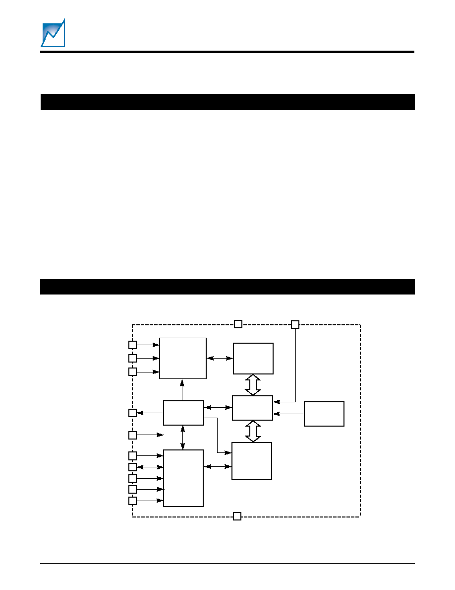
FUNCTIONAL BLOCK DIAGRAM
FEATURES
l
SMD1102
w
2-Channel Analog Input
w
External Voltage Reference Input Provided for
Absolute Measurements
l
SMD1103
w
3-Channel Analog Input
w
Reference Voltage Input for the A/D Converter
is Connected to V
DD
for Ratiometric Measure-
ments
l
SMD1113
w
Extended I
2
C Operation
GND
VDD
CONVERTER
CLOCK
SCL
SDA
2033 BD 7.0
CONTROL
LOGIC
2-WIRE
SERIAL
INTERFACE
ANALOG
MULTIPLEXER
10-BIT A/D
CONVERTER
E2PROM
ALARM LIMIT
REGISTERS
SAMPLE
AND
HOLD
SMBALERT#
AIN2 X
AIN1
AIN0
(1103,
1113)
REFIN
(1102,
1113)
X
CE#
A2
A1
A0
(1113)
(1113)
(1113)
(1113)
2
SMD1102 / 1103 / 1113
2033 7.5 4/9/01
SUMMIT MICROELECTRONICS, Inc.
PIN CONFIGURATION
The SMD1102, SMD1103 and SMD1113 each contain a
10-Bit data acquisition system (DAS) with dedicated EE-
PROM alarm limit storage. The three devices communi-
cate with the host µP via a standard two-wire I
2
C serial
interface. After initialization the SMD1102/1103/1113 can
INTRODUCTION
PIN NAMES
automatically monitor one or more analog input channels.
If any input signal moves beyond its user-programmed
limits the host is notified by the SMB
ALERT
#
output, enabling
fault prediction in telecom line card applications, as an
example.
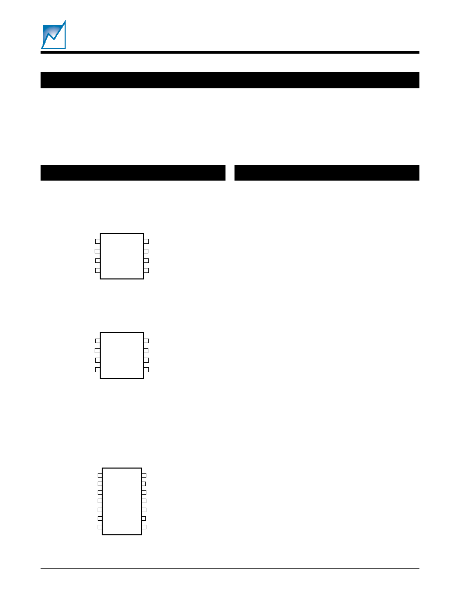
1102 & 1103
A
IN
0, A
IN
1, A
IN
2
Analog channel inputs
GND
Power supply return
REF
IN
Reference input
SCL
Serial Clock
SDA
Serial Data
SMB
ALERT
#
Interrrupt output
V
DD
Power Supply
1113
CE#
Chip Enable
A2, A1, A0
I
2
C Address select inputs
A
IN
0, A
IN
1, A
IN
2
Analog channel inputs
GND
Power supply return
REF
IN
Reference input
SCL
Serial Clock
SDA
Serial Data
SMB
ALERT
#
Interrrupt output
V
DD
Power Supply
A
IN
2
A
IN
1
A
IN
0
GND
V
DD
SMB
ALERT
#
SCL
SDA
1
2
3
4
8
7
6
5
8-Pin PDIP
or 8-Pin SOIC
SMD1103
2033 8 PCon
REF
IN
A
IN
1
A
IN
0
GND
V
DD
SMB
ALERT
#
SCL
SDA
1
2
3
4
8
7
6
5
8-Pin PDIP
or 8-Pin SOIC
SMD1102
A0
A1
A2
A
IN
2
A
IN
1
A
IN
0
GND
V
DD
CE#
REF
IN
NC
SMB
ALERT
#
SCL
SDA
1
2
3
4
5
6
7
14
13
12
11
10
9
8
2033 14 PCon
14-Pin SOIC
SMD1113
3
2033 7.5 4/9/01
SMD1102 / 1103 / 1113
SUMMIT MICROELECTRONICS, Inc.
*COMMENT
Stresses listed under Absolute Maximum Ratings may cause perma-
nent damage to the device. These are stress ratings only, and
functional operation of the device at these or any other conditions
outside those listed in the operational sections of this specification is not
implied. Exposure to any absolute maximum rating for extended
periods may affect device performance and reliability.
Temperature Under Bias ...................... ≠55∞C to 125∞C
Storage Temperature ........................... ≠65∞C to 150∞C
Lead Solder Temperature (10 seconds) ............. 300 ∞C
Terminal Voltage with Respect to GND:
All ......................................... ≠2V to 7V
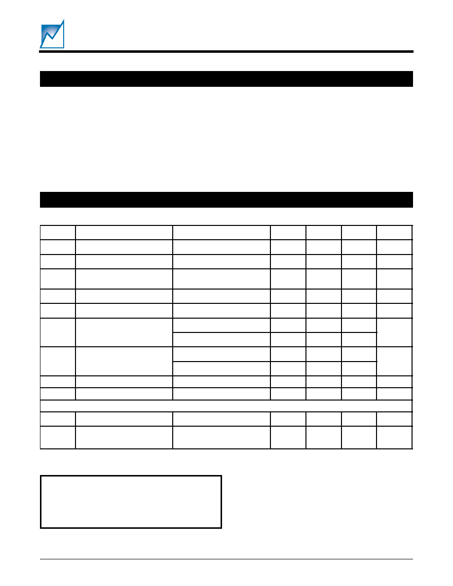
DC OPERATING CHARACTERISTICS
ABSOLUTE MAXIMUM RATINGS*
(Over Recommended Operating Conditions; Voltages are relative to GND)
2033 Elect Table
l
o
b
m
y
S
r
e
t
e
m
a
r
a
P
s
n
o
i
t
i
d
n
o
C
)
1
e
t
o
N
(
.
n
i
M
.
p
y
T
.
x
a
M
s
t
i
n
U
V
C
C
e
g
a
t
l
o
V
y
l
p
p
u
S
7
.
2
5
.
5
V
I
C
C
t
n
e
r
r
u
C
y
l
p
p
u
S
n
e
p
o
s
t
u
p
t
u
o
ll
A
3
A
m
I
B
S
t
n
e
r
r
u
C
y
b
d
n
a
t
S
,
e
l
d
i
C
D
A
,
n
e
p
o
s
t
u
p
t
u
o
ll
A
s
s
e
c
o
r
p
n
i
y
r
o
m
e
m
o
n
0
5
A
µ
I
I
L
t
n
e
r
r
u
c
e
g
a
k
a
e
l
t
u
p
n
I
V
N
I
V
o
t
V
0
=
C
C
2
A
µ
I
O
L
t
u
O
t
n
e
r
r
u
c
e
g
a
k
a
e
l
t
u
p
V
T
U
O
V
o
t
V
0
=
C
C
0
1
A
µ
V
L
O
e
g
a
t
l
o
v
w
o
l
t
u
p
t
u
O
V
C
C
I
,
V
5
=
L
O
A
m
1
.
2
=
4
.
0
V
V
C
C
I
,
V
5
.
4
<
L
O
A
m
1
=
2
.
0
V
H
O
e
g
a
t
l
o
v
h
g
i
h
t
u
p
t
u
O
V
C
C
I
,
V
5
=
L
O
A
µ
0
0
4
≠
=
4
.
2
V
V
C
C
I
,
V
5
.
4
<
L
O
A
µ
0
0
1
≠
=
V
C
C
2
.
0
≠
V
L
I
e
g
a
t
l
o
v
w
o
l
t
u
p
n
I
1
.
0
≠
3
.
0
◊
V
C
C
V
V
H
I
e
g
a
t
l
o
v
h
g
i
h
t
u
p
n
I
7
.
0
◊
V
C
C
V
C
C
7
.
0
+
V
s
t
u
p
n
I
g
o
l
a
n
A
V
N
I
F
E
R
V
F
E
R
e
g
a
t
l
o
v
t
u
p
n
i
1
V
C
C
V
V
N
I
A
n
o
e
g
a
t
l
o
v
t
u
p
n
I
N
I
0
A
h
g
u
o
r
h
t
N
I
2
0
5
.
5
V
RECOMMENDED OPERATING CONDITIONS
Temperature
≠40
∫
C to 85
∫
C.
Voltage
2.7V to 5.5V

4
SMD1102 / 1103 / 1113
2033 7.5 4/9/01
SUMMIT MICROELECTRONICS, Inc.
PIN DESCRIPTIONS
Serial Clock (SCL)
The SCL input is used to clock data into and out of the
device. In the WRITE mode data must remain stable while
SCL is HIGH. In the READ mode data is clocked out on
the falling edge of SCL.
Serial Data (SDA)
The SDA pin is a bidirectional pin used to transfer data into
and out of the device. Data may change only when SCL
is LOW, except during START and STOP conditions. It is
an open-drain output and may be wire-ORed with any
number of open-drain or open-collector outputs.
SMB
ALERT
This interrupt output pin signals the host when an out-of-
limit condition is detected by one of the EEPROM limit
registers. The SMB
ALERT
open-drain output is active low.
REF
IN
Voltage reference input for 10-Bit A/D converter. This
signal is only on the SMD1102 and SMD1113.
A
IN
0, A
IN
1, A
IN
2
Multiplexer input pins for channels 0, 1, and 2, respec-
tively. A
IN
2 is only available on the SMD1103 and
SMD1113.
A0, A1, A2
The address inputs are only used in the SMD1113. They
allow multiple SMD1113s on a single bus. A2 has a 50k
pull-up resistor, and A1 and A0 have 50k
pull-down
resistors. Do not set to all zeroes to avoid conflict with the
SMB Alert Response.
CE#
Chip Enable/disable input. A GND level enables.
SMD1113 only. It has a 50k
pull-down resistor.
V
DD
Power supply input.
GND
Power supply return.
5
2033 7.5 4/9/01
SMD1102 / 1103 / 1113
SUMMIT MICROELECTRONICS, Inc.
DEVICE OPERATION
The SMD1102, SMD1103 and SMD1113 Data Acquisition
Systems (DAS) are each comprised of: an analog input
multiplexer, sample-and-hold circuit, 10-Bit successive
approximation Analog-to-Digital (A/D) Converter, and
nonvolatile EEPROM memory to store upper and lower
alarm-limits for each input channel. The user programs
the alarm limits via the industry-standard I
2
C interface. An
SMB
ALERT
#
interrupt output signals if any of the analog
inputs move outside these limits.
DAS Modes of Operation
The SMD1102/1103/1113 have four user-selectable
modes of operation. These modes are: a single conver-
sion of one channel, successive conversions on the same
channel, sequential conversions on all three channels, or
autonomous conversions of the same or all channels.
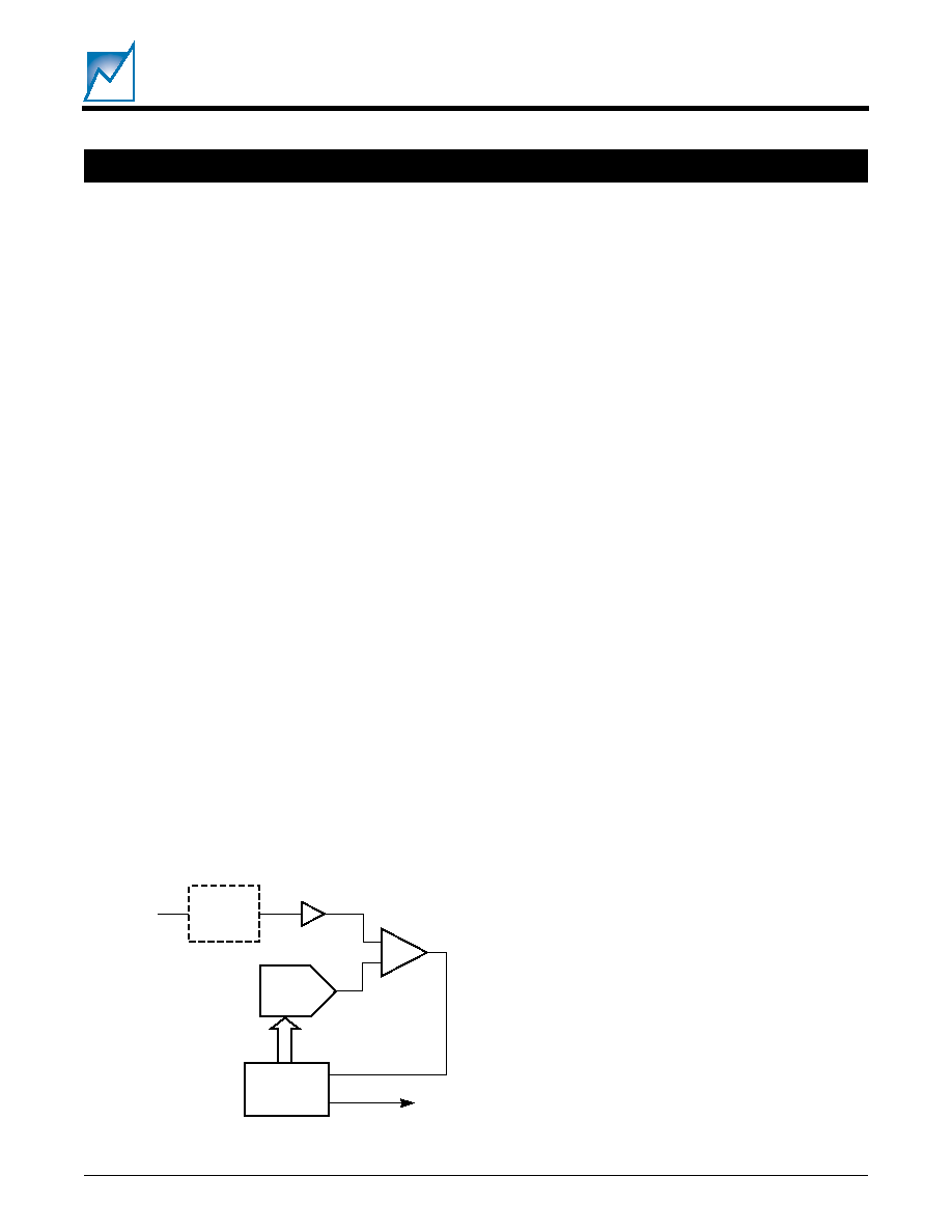
Sample-and-Hold Operation
The channel switching and sampling architecture of the A/
D's comparator is illustrated in the equivalent input circuit
diagram in Figure 1. During acquisition the selected
channel charges a capacitor in the sample-and-hold cir-
cuit. The acquisition interval spans the Acknowledge
period following the command byte and ends on the rising
edge of the 1st clock. At the end of the acquisition phase
the analog input is disconnected, retaining charge on the
hold capacitor as a sample of the signal.
Addressing and Command Sequence
All operations of the DAS are preceded first by the start
condition and then by the addressing command se-
quence. For the SMD1102 & SMD1103 this is 1001
BIN;
for
the SMD1113 it is the binary values of "A2, A1, A0, 1" --
a four bit number. The next bit in the addressing sequence
is the EEPROM/Conversion bit; when set to zero the
Figure 1. Sample/Hold and SAR
+
≠
2033 Fig01 2.0
Analog In
Buffer
DAC
SAR
Sample
& Hold
SDA
device is instructed to perform an A/D conversion, and
when set to logic one the EEPROM limit register will be
addressed. The next two bits are the channel select bits.
If the channel select bits are set to 11
BIN
, and the conver-
sion bit is set to 0, then auto-increment is enabled. In the
auto-increment mode conversions are performed on suc-
cessive channels, starting with channel 0. After channel
2 is converted (channel 1 on the SMD1102) the address
will wrap around to channel 0. The last bit is the Read/
Monitor bit. When mode select is set to logic 1, data can
be read from a conversion or from one of the EEPROM
limit registers, depending on the state of the conversion
bit. When the mode select bit is logic zero either the auto-
monitor mode is entered or the EEPROM limit register is
programmed, again depending on the state of the conver-
sion bit. See Table 1.
Single Channel Conversions
The command sequence is the Device Type Identifier,
followed by the conversion bit set to zero and the channel
select bits set to the desired value and R/M set to logic one.
After the R/M bit is clocked in the host releases the SDA
line and monitors the SDA line for an acknowledge bit
(ACK) from the SMD1102/1103/1113. The device will
drive the SDA line low indicating it received the command
and that it has initiated the acquisition and conversion on
the selected channel. The clock source for the acquisition
and conversion is an internal clock. After the ACK the
SMD1102/1103/1113 will output four dummy zeros on
SDA followed by an echo of the channel's 2 address bits.
The remaining bits in this first byte are the two MSBs of the
conversion. Refer to Figure 2 for a detailed illustration of
this sequence, and for that of retrieving the remaining
conversion byte. The host can issue a stop condition after
retrieving the conversion data and place the SMD1102/
1103/1113 in a low power standby mode.
Successive Single Channel Conversions
If the host does not issue a stop command after receiving
the last bit of the previous conversion, but instead issues
an ACK and continues clocking, then the SMD1102/1103/
1113 will begin another acquisition and conversion pro-
cess on the same channel.
Auto-Increment
In the auto-increment mode, the DAS starts a conversion
and then automatically advances to the next channel. The
auto-increment mode always starts at channel 0 and
switches the channel input in the sequence 0, 1, 2, 0, 1, 2,
etc. (SMD1103) after each successive conversion. The