SUMMIT MICROELECTRONICS, Inc. ∑ 300 Orchard City Drive, Suite 131 ∑ Campbell, CA 95008 ∑ Telephone 408-378-6461 ∑ Fax 408-378-6586 ∑ www.summitmicro.com
1
Characteristics subject to change without notice
© SUMMIT MICROELECTRONICS, Inc. 1999
2037 8.4 10/26/00
SUMMIT
MICROELECTRONICS, Inc.
SMH4042
VGATE3
VGATE5
ISLEW
BD_SEL1#
SGNL_VLD#
HEALTHY#
VCC5
HST_3V_MON
VSEL
PCI_RST#
CARD_3V_MON
CARD_5V_MON
+
-
LOCAL_PCI_RST#
LOCAL_PCI_RST
DRVREN#
+
-
+
-
EEPROM
Memory
Array
A2
SCL
SDA
A1
A0
BD_SEL2#
+
-
+
-
+
-
PWR_EN
FAULT#
1Vref
1.25V
Slew Rate
Control
Charge
Pump
Ref
Voltage
Control
Circuitry
50mV
_+
_+
50mV
CBI_3
CBI_5
2037 ILL2.2
FEATURES
∑
Full Voltage Control for Hot Swap Applications
CompactPCI High Availability Compatible
-
On-board 15V High Side Driver Generation
Allows use of Low On-resistance N-Channel FETS
-
Undervoltage Lockout
-
Electronic Circuit Breakers
-
Card Insertion Detection
-
Host VCC Detection
-
Card Voltage Sequencing
∑
Flexible Reset Control
-
Low Voltage Resets
-
Host Reset Filtering
-
Soft Reset
∑
Adjustable Power-on Slew Rate
∑
Supports Mixed Voltage Cards
∑
Integrated 4K Bit 2-Wire E
2
PROM Memory
-
Data DownloadTM Mode [Simplifies
Downloading of Configuration Memory into
Interface ASIC or MCU]
APPLICATIONS
∑
CompactPCI Hot Swap Control
∑
VME Live Insertion Control
Hot SwapTM Controller
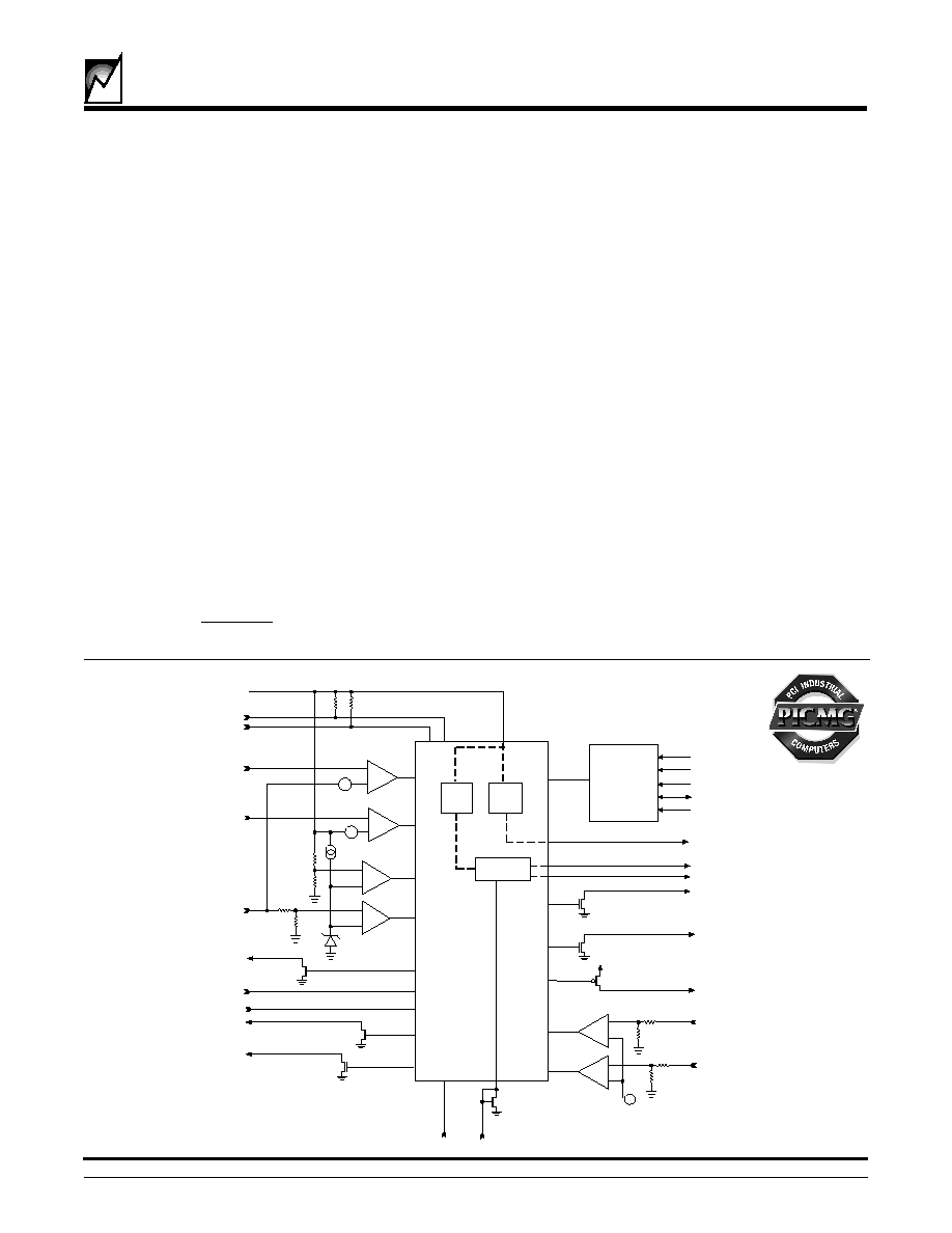
DESCRIPTION
The SMH4042 is a fully integrated hot swap controller that
provides complete power control for add-in cards ranging
in use for basic hot swap systems to high availability
systems. It detects proper insertion of the card and
senses valid supply voltage levels at the backplane.
Utilizing external low on-resistance N-channel
MOSFETs, card power is ramped by two high-side driver
outputs that are slew-rate limited at 250V/s.
The SMH4042 continuously monitors the host supplies,
the add-in card supplies and the add-in card current. If the
SMH4042 detects the current is higher than the pro-
grammed value it will shut down the MOSFETs and issue
a fault status back to the host.
The on board E
2
PROM can be used as configuration
memory for the individual card or as general purpose
memory. The proprietary DataDownload mode provides
a more direct interface to the E
2
PROM, simplifying access
by the add-in card's controller or ASIC.
FUNCTIONAL BLOCK DIAGRAM
ASSOCIATE
M E M B E R
2
SMH4042
2037 8.4 10/26/00
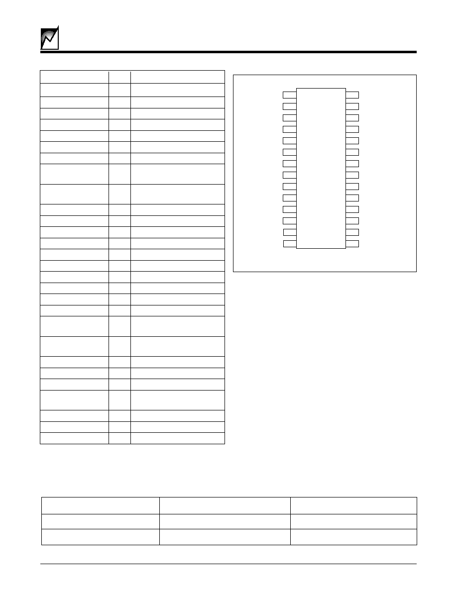
PIN CONFIGURATIONS SOIC and SSOP
RECOMMENDED OPERATING CONDITIONS
Condition
Min
Max
Temperature
-40∞C
+85∞C
V
CC
2.7V
5.5V
2037 PGM T2.0
Symbol
Pin
Description
CBI_5
1
Circuit Breaker Input (5V)
DRVREN
#
2
High Side Driver Enable
ISLEW
3
Slew Rate Control
FAULT
#
4
Fault Output Active Low
1Vref
5
1Volt Reference Output
VSEL
6
Voltage Select Input
PWR_EN
7
Power On Enable Input
A0
8
Memory Address 0
(NC or Gnd)
LOCAL_PCI_RST#
9
Back End Reset Output
(Active Low)
A1
10
Memory Address 1
A2
11
Memory Address 2
BD_SEL2#
12
Board Select 2
BD_SEL1#
13
Board Select 1
GND
14
Ground
HEALTHY
#
15
Backend Power On
SGNL_VLD#
16
Signals Valid Output
PCI_RST#
17
Host reset input
SDA
18
Serial Data I/O
SCL
19
Serial Clock Input
LOCAL_PCI_RST
20
Back End Reset
Output
(Active High)
CARD_3V_MON
21
Card-side 3 Volt
Monitor Input
VGATE3
22
High Side Drive Output
HST_3V_MON
23
Host 3V Monitor Input
CBI_3
24
Circuit Breaker Input (3V)
CARD_5V_MON
25
Card-side 5 Volt
Monitor Input
NC
26
No Connect
VGATE5
27
High Side Drive Output
V
CC
28
Supply Voltage
2037 PGM T1.2
1
2
3
4
5
6
7
8
9
10
11
12
24
23
22
21
20
19
18
17
16
15
27
28
VCC
VGATE5
CARD_5V_MON
HST_3V_MON
VGATE3
CARD_3V_MON
SDA
SGNL_VLD#
HEALTHY#
GND
BD_SEL2#
CBI_5
DRVREN#
ISLEW
VSEL
PWR_EN
A0
LOCAL_PCI_RST#
A1
A2
PCI_RST#
1Vref
13
14
25
26
CBI_3
BD_SEL1#
LOCAL_PCI_RST
FAULT#
SCL
NC
2037 ILL1.2
3
2037 8.4 10/26/00
SMH4042
*COMMENT
Stresses listed under Absolute Maximum Ratings
may cause permanent damage to the device. These
are stress ratings only, and functional operation of
the device at these or any other conditions outside
those listed in the operational sections of this speci-
fication is not implied. Exposure to any absolute
maximum rating for extended periods may affect
device performance and reliability.
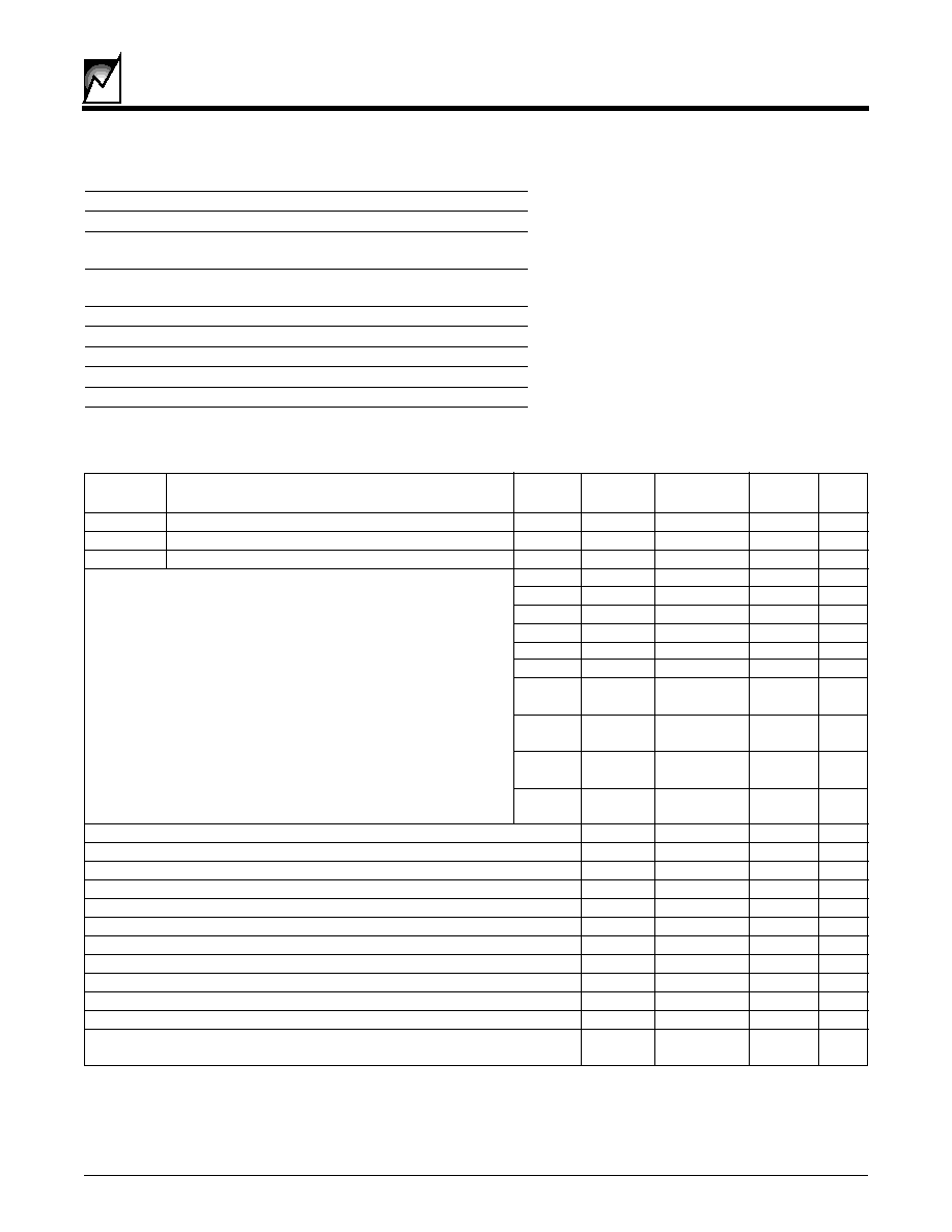
ABSOLUTE MAXIMUM RATINGS*
Temperature Under Bias
-55∞C to +125∞C
Storage Temperature
-65∞C to +150∞C
Voltage on :
HST_3V_MON, CARD_3V_MON
7V
V
CC
, CARD_5V_MON
SGNL_VLD#, HEALTHY
#
&
7V
LOCAL_PCI_RESET#
VGATE3, VGATE5, DRVREN
#
16V
RESET
V
CC
+.7V
All Others
V
CC
+.7V
Output Short Circuit Current
100mA
Lead Solder Temperature (10 secs)
300∞C
Symbol
Parameter
Part no.
Min.
Typ.
Max.
Units
Suffix
V
CC
Operating Voltage
See Note 1
1
V
I
CC1
Power Supply Current
Operating
500
µA
I
CC2
Power Supply Current
Writing
3
mA
V
TRIP
V
TRIP
Threshold Levels
V
CC
5
A
4.250
4.375
4.50
V
V
CC
5
B
4.50
4.625
4.75
V
HST_3V_MON
G
2.57
2.65
2.72
V
HST_3V_MON
H
2.72
2.8
2.87
V
HST_3V_MON
K
2.87
2.95
3.0
V
HST_3V_MON
L
3.0
3.1
3.17
V
CARD_5V_MON
M
V
CC
5 V
TRIP
V
+50mV
CARD_5V_MON
N
V
CC
5 V
TRIP
V
-50mV
CARD_3V_MON
M
HST_3V_MON
V
+50mV
CARD_3V_MON
N
HST_3V_MON
V
-50mV
V
TRHST
Trip Point Hysteresis
7
mV
I
LI
Input Leakage Current
2
µA
I
LO
Output Leakage Current
10
µA
V
IL
Input Low Voltage
-0.1
0.8
V
V
IH
Input High Voltage
2
V
CC
+1V
V
V
OL
Output Low Voltage, V
CC
= 5.0V, I
OL
= 2.1mA
0.4
V
V
OH
Output High Voltage, V
CC
= 5.0V, I
OH
= -400µA
2.4
V
V
OLRS
LOCAL_PCI_RESET# Output Low Voltage, I
OL
= 3.2mA
0.4
V
V
OHRS
RESET Output High, I
OH
= -800µA
V
CC
-.75V
V
V
OHVG
VGATE3, VGATE5 Output Voltage, I
OH
= 20µA
13
14
15
V
V
REF
Reference Output Voltage, No Load
0.95
1
1.05
V
V
CB
Circuit Breaker Trip Voltage, V
CB
(V
CC
-CBI_5) or
40
50
60
mV
V
CB
=(HST_3V_MON-CBI_3)
DC ELECTRICAL CHARACTERISTICS T
A
= -40∞C to +85∞C
2037 PGM T3.4
Notes:
1. The SMH4042 will drive the reset outputs and voltage control signals to valid levels throughout the operating range of 1V to 5.5V.
The balance of the logic will not be guaranteed operational unless V
CC
is greater than 2.7V.
2. Refer to the ordering information table for all valid combinations of options.
4
SMH4042
2037 8.4 10/26/00
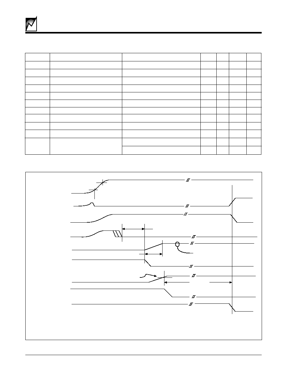
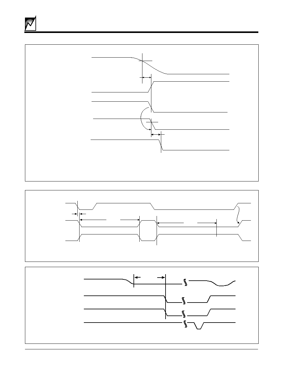
Card Insertion Timing Diagram
V
TRIP
V
RVALID
VCC
&
HST_3V_MON
LOCAL_PCI_RST#
RESET
BD_SEL1#
+
BD_SEL2#
VGATE5 & VGATE3
DRVREN#
CARD_5V_MON
&
CARD_3V_MON
HEALTHY#
SGNL_VLD#
V
TRIP
t
PURST
t
SLEW
t
HSE
V
OHVG
2037 ILL3.0
Symbol
Parameter
Notes
Min.
Typ.
Max.
Units
t
VTPD
V
TRIP
to Power Down Delay
Host Voltage Input
1
5
µs
t
VTR
V
TRIP
to RESET Output Delay
Card Voltage Input
1
5
µs
t
PRLPR
PCI_RST# to LOCAL_PCI_RST#
.1
1
µs
V
RVALID
RESET Output Valid
1
V
T
SLEW
Slew Rate
250
V/Sec
T
HSE
BD-SEL# to Power-on Delay
BD_SEL# Noise filter
100
150
200
ms
t
PURST
Reset Timeout
100
150
200
ms
t
GLTICH
Glitch Reject Pulse Width
40
ns
t
OCF
Over-current to FAULT
#
1
µs
t
OCVG
Over-current to VGATE Off
1
µs
t
CBTC
Circuit Breaker Time Constant
Powering-on
4
µs
Operating
16
µs
SEQUENCER AC OPERATING CHARACTERISTICS (Over Recommended Operating Conditions)
2037 PGM T4.1
5
2037 8.4 10/26/00
SMH4042
Loss of Voltage Timing Sequence
Circuit Breaker Timing Diagram
Host Initiated Reset Timing Diagram
VCC
or
HST_3V_MON
VGATE5
&
VGATE3
LOCAL_PCI_RST#
&
HEALTHY#
SGNL_VLD#
&
DRVREN#
t
VTPD
CARD_5V_MON
or
CARD_3V_MON
V
TRIP
V
TRIP
t
VTR
2037 ILL4.0
t
PRLPR
PCI_RST#
LOCAL_PCI_RST#
RESET
t
PURST
t
PURST
2037 ILL5.0
t
CBTC
CBI_5 or CBI_3
FAULT#
VGATE5 & VGATE3
PCI_RST#
2037 ILL6.0
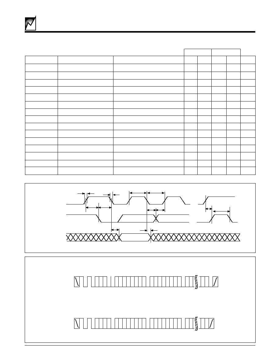
6
SMH4042
2037 8.4 10/26/00
2.7V to 4.5V
4.5V to 5.5V
Symbol
Parameter
Conditions
Min
Max
Min
Max
Units
fSCL
SCL Clock Frequency
0
100
0
400
KHz
tLOW
Clock Low Period
4.7
1.3
µs
tHIGH
Clock High Period
4.0
0.6
µs
tBUF
Bus Free Time
Before New Transmission
4.7
1.3
µs
tSU:STA
Start Condition Setup Time
4.7
0.6
µs
tHD:STA
Start Condition Hold Time
4.0
0.6
µs
tSU:STO
Stop Condition Setup Time
4.7
0.6
µs
tAA
Clock Edge to Valid Output
SCL low to Valid SDA (cycle n)
0.3
3.5
0.2
0.9
mµs
tDH
Data Out Hold Time
SCL low (cycle n+1) to SDA change
0.3
0.2
µs
tR
SCL and SDA Rise Time
1000
300
ns
tF
SCL and SDA Fall Time
300
300
ns
tSU:DAT
Data In Setup Time
250
100
ns
tHD:DAT
Data In Hold Time
0
0
ns
TI
Noise Filter SCL & SDA
Noise Suppression
100
100
ns
tWR
Write Cycle Time
5
5
ms
MEMORY AC OPERATING CHARACTERISTICS
T
A
= -40∞C to +85∞C
2037 PGM T5.1
tSU:STO
tBUF
tSU:DAT
tHD:DAT
tDH
tHIGH
tLOW
tR
tF
tSU:SDA
tHD:SDA
SDA Out
SDA In
SCL
tAA
2037 ILL11.0
A
C
K
A
2
A
1
B
0
R
/
W
A
C
K
D
7
D
6
D
5
D
4
D
3
D
2
D
1
D
0
A
C
K
D
7
D
6
D
1
D
0
S
T
O
P
S
T
A
R
T
D
7
D
6
D
5
D
4
D
3
D
2
D
1
D
0
S
T
A
R
T
A
C
K
A
2
A
1
B
0
R
/
W
A
7
A
6
A
5
A
4
A
3
A
2
A
1
A
0
A
C
K
D
7
D
6
D
5
D
4
D
3
D
2
D
1
D
0
A
C
K
D
7
D
6
D
1
D
0
A
C
K
S
T
O
P
Typical Write Operation
Typical Read Operation
Master
SDA
Slave
Master
SDA
Slave
2037 ILL12.0
7
2037 8.4 10/26/00
SMH4042
PIN DESCRIPTIONS
CBI_5: CBI_5 is the circuit breaker input for the supply
voltage. With a series resistor placed in the supply path
between the 5V early power and CBI_5, the circuit
breaker will trip whenever the voltage across the resistor
exceeds 50mV.
DRVREN
#
: DRVREN
#
is an open-drain, active-low out-
put that indicates the status of the 3 volt and 5 volt high
side driver outputs (VGATE5 and VGATE3). This signal
may also be used as a switching signal for the 12 volt
supply.
FAULT#: FAULT# is an open-drain, active-low output. It
will be driven low whenever an over-current condition is
detected. It will be reset at the same time that the VGATE
outputs are turned back on after a reset from the host on
the PWR_EN pin.
1Vref: The 1Vref output provides a 1 volt reference for
pre-charging the bus signal pins. Implementing a simple
unity-gain amplifier circuit will allow pre-charging a large
number of pins.
ISLEW: ISLEW is a Diode-connected NFET input. It may
be used to adjust the 250V/s default slew rate of the high-
side driver outputs
VSEL: VSEL is a TTL level input used to determine which
of the host power supply inputs will be monitored for valid
voltage and reset generation. This is a static input and the
pin should be tied to V
CC
or ground through a resistor.
A0: Address 0 is not used by the memory array. It can be
connected to ground or left floating. It must not be
connected V
CC
.
A1, A2: Address inputs 1 and 2 are used to set the two-
bit device address of the memory array. The state of these
inputs will determine the device address for the memory
if it is on a two-wire bus with multiple memories with the
same device type identifier. (For complete addressing
information refer to the detailed memory operation sec-
tion that follows.)
SCL: The SCL input is used to clock data into and out of
the memory array. In the write mode, data must remain
stable while SCL is HIGH. In the read mode, data is
clocked out on the falling edge of SCL.
SDA: The SDA pin is a bidirectional pin used to transfer
data into and out of the memory array. Data changing from
one state to the other may occur only when SCL is LOW,
except when generating START or STOP conditions.
SDA is an open-drain output and may be wire-ORed with
any number of open-drain outputs.
BD_SEL1# BD_SEL2#: These are active low TTL level
inputs with internal pull-ups to V
CC
. When pulled low they
indicate full board insertion. When used in a "non-High
Availability" application these inputs will be the last con-
nector pins to make contact with the host backplane. On
the host side, the signals should be directly tied to ground.
In a "High Availability" application these inputs can be the
last pins to mate with the backplane. Alternatively, they
can be actively driven by the host or be connected to
switches interfaced to the board ejectors or any combina-
tion. Regardless, BOTH inputs MUST be low before the
SMH4042 will begin to turn on the backend voltage.
GND: Ground should be applied at the same time as
early-power.
HEALTHY
#
: HEALTHY
#
is an open-drain, active-low
output indicating card side power inputs are above their
reset trip levels.
SGNL_VLD#: SGNL_VLD# is an open-drain, active-low
output that indicates card side power is valid and the
internal card side PCI_RST# timer has timed out.
PWR_EN: PWR_EN is a TTL level input that allows the
host to enable or disable the power to the individual card.
During initial power up, this signal would start in a low state
and then be driven high during software initialization. If
this signal is driven low, the power supply control outputs
will be driven into the inactive state, and the reset signals
asserted. In a "non-High Availability" system this input can
be tied high.
The PWR_EN input is also used to reset the SMH4042
circuit breakers. After an over-current condition is de-
tected the VGATE outputs can be turned back on by first
taking PWR_EN low then returning it high.
PCI_RST#: PCI_RST# is a TTL level input used as a reset
input signal from the host interface. A high to low transition
(held low longer than 40ns) will initiate a reset sequence.
The LOCAL_PCI_RST# output and the RESET output
will be driven active for a minimum period of tPURST. If
the PCI_RST# input is held low longer than tPURST the
reset outputs will continue to be driven until PCI_RST# is
released.
VSEL-Voltage
Host Voltage
Select
Monitored
Low
5 Volt or Mixed-Mode
High
3.3 Volt Only

8
SMH4042
2037 8.4 10/26/00
LOCAL_PCI_RST#: LOCAL_PCI_RST# is an open-
drain active-low output. It is used to reset the backend
circuitry on the add-in card. It is active whenever the card-
side monitor inputs are below their respective V
TRIP
levels. It may also be driven low by a low input on the
PCI_RST# pin.
LOCAL PCI_RST: LOCAL PCI_RST is an open-drain
(PFET) active-high output. It operates in parallel with
LOCAL_PCI_RST# providing an active high reset signal
which is required by many 8051 style MCUs. It is active
whenever the card-side monitor inputs are below their
respective V
TRIP
levels. It may also be driven active by a
low input on the PCI_RST# pin.
CARD_3V_MON: The CARD_3V_MON input monitors
the card-side 3.3V supply. If the input falls below V
TRIP
,
the HEALTHY
#
and SIGNL_VLD# outputs are de-as-
serted and the reset outputs are driven active.
VGATE3: VGATE3 is a slew rate limited high side driver
output for the 3.3V external power FET gate. The
VGATE3 output-voltage is generated by an on-board
charge pump.
HST_3V_MON: The HST_3V_MON input monitors the
host 3.3 volt supply and it is used as a reference for the
circuit breaker comparator. If VCC3 falls below V
TRIP
,
SGNL_VLD# is de-asserted, the high side drivers are
disabled and LOCAL_PCI_RST# is asserted.
CBI_3: CBI_3 is the circuit breaker input for the low
supply. With a series resistor placed in the supply path
between VCC3 and CBI_3, the circuit breaker will trip
whenever the voltage across the resistor exceeds 50mV.
CARD_5V_MON: The CARD_5V_MON input monitors
the card-side 5V supply. If the input falls below V
TRIP
, the
HEALTHY
#
and SIGNL_VLD# outputs are de-asserted
and the reset outputs are driven active.
VGATE5: VGATE5 is a slew rate limited high side driver
output for the 5V external power FET gate. The output
voltage is generated by an on-board charge pump.
V
CC
: V
CC
is the power supply pin for the SMH4042 This
input is monitored for power integrity. If it falls below the
5V sense threshold (VTRIP) and the VSEL input is low,
the SGNL_VLD# HEALTHY
#
signals are de-asserted,
the high side drivers disabled and reset outputs are
asserted. On a
CompactPCI board, this must be con-
nected to early power.
DEVICE OPERATION
Power-Up Sequence
The SMH4042 is an integrated power controller for any
hot swappable add-in card. The SMH4042 provides all
the signals and control functions to be compatible with
CompactPCI Hot Swap requirements for basic hot swap
systems, full hot swap boards and high availability sys-
tems.
Insertion Process
As the add-in board is inserted into the backplane physical
connections should be made with the chassis in order to
properly discharge any voltage potentials to ground. The
board will first contact the long pins on the backplane that
provide early power (+5V, +3.3V and ground). Depending
upon the board configuration early power should be
routed to the VCC pin of the SMH4042. As soon as power
is applied, the SMH4042 will assert the reset outputs to
the backend circuits, turn off the VGATE3/5 outputs
(disabling the external power FETS) and begin outputting
the 1-volt Vref. The 1-volt reference can be used to pre-
charge the I/O pins before they begin to mate with the bus
signals. The open collector HEALTHY
#
output will be de-
asserted, It should be actively pulled high by an external
pull-up resistor (minimum 10K ohm).
The next pins to mate are the I/Os and the balance of the
power pins, if they are not already mated. The I/Os will
have been pre-charged by the Vref output of the
SMH4042.
The BD_SEL# pins are the last inputs to be driven to their
true state. In most systems these will most likely be driven
to ground when the short pins are mated. This would
indicate the card is fully inserted and the power-up se-
quence can begin. If, however, the design is based on
high availability requirements the two pins can be actively
driven by the host or combined with a switch input indicat-
ing the ejector handles are fully engaged.
Sequencing
Once the proper card insertion has been assured, the
SMH4042 will check the status of the Power Enable signal
from the host. This input can be used to power down
individual cards on the bus via software control; it must by
held high in order for the SMH4042 to enable power
sequencing to the card.
Once these conditions are met, the SMH4042 will drive
the VGATE3 and VGATE5 outputs to turn on the external
3 volt and 5 volt power FETs. The slew rate of these
outputs is controlled using on board circuitry and results
in a slew rate of 250V/s. Different slew rates can be
9
2037 8.4 10/26/00
SMH4042
accommodated by either adding an additional capacitor
between the MOSFET gate and ground or by injecting
current into the ISLEW input. All circuitry on the card is
held in a reset condition until the 5 volts (or 3.3 volt) supply
is stable and the reset interval timer has timed out the
150ms reset time. At this point, the reset signals are de-
asserted, and proper operation of the card commences.
The SMH4042 will monitor the card's backend voltages.
Once they are at or above the CARD VTRIP levels, the
SMH4042 will drive the HEALTHY
#
output.
Card Removal Process
The card removal process operates in the opposite se-
quence. For non-high-availability cards, the action of card
removal disconnects the BD_SEL# (short pins) from
ground and the SMH4042 will instantly shutdown the
VGATE outputs, change the HEALTHY# status and as-
sert the LOCAL_PCI_RST# output.
Because connectors to the host backplane employ the
staggered pins, power will still be applied to the SMH4042
and the I/O interface circuits. The LOCAL_PCI_RST#
signal will place the interface circuits into a high imped-
ance condition. The pre-charge voltage will be applied to
the I/Os enabling a graceful disengagement from the
active bus. Once the I/O pins are free of the backplane
power can then be removed from the SMH4042 and other
early power devices by releasing the long pins.
The removal process is slightly different for a high-avail-
ability system. As the ejector handle is rotated the ejector
switch will open, causing a change of state that will
activate the ENUM# signal to the host. In response to this
notification the host will de-assert a hardware controlled
BD_SEL# signal. This action will turn on an indicator LED
on the card, notifying the operator it is now safe to proceed
with the removal of the card. The sequence will then follow
that outlined for the non-high-availability removal pro-
cess.
Power Configurations
The SMH4042 can be used in 5V-only, 3.3V-only and
mixed voltage systems. For mixed voltage systems, sim-
ply connect the appropriate bus and card power inputs as
indicated. The V
SEL
pin should be grounded.
For systems with a single power supply, connect V
CC
and
HST_3V_MON together to the bus power line. Also con-
nect CARD_3V_MON and CARD_5V_MON together to
the card side power. Now the state of VSEL determines
the reset level that will be used to signal valid power. For
3.3V systems, tie VSEL to VCC, for 5V systems, tie VSEL
to ground.
MONITORING POWER SUPPLY HEALTH
Monitor Inputs
The SMH4042 has a total of six comparators that are used
to monitor the health of the host platform supplies and the
card-side (backend) voltages. In hot swap applications
each supply going to the backend logic needs to be
monitored at three points.
The first point is at the source on the host connector, V
CC
and HST_3V_MON. If this voltage is not within specifica-
tion, then the down stream sequencing of powering-on
the backend logic will not proceed.
The next stage (the CBI inputs) is one step closer to the
backend logic to monitor the current flowing into the
backend logic. This can not exceed the specification;
however, If it does, then the SMH4042 must turn off the
source to the backend logic.
The CARD_5V_MON and CARD_3V_MON inputs are
used to sense the actual voltage level in the backend
logic. If either comparator detects a low voltage condition
the backend logic will be placed in a reset condition
(LOCAL_PCI_RST# asserted), but the VGATE outputs
will remain active so long as the host voltage and current
sense are valid.
V
CC
vs. HST_3V_MON
The V
CC
input is the supply input and in a CompactPCI
application this pin must connect to an early power pin on
the host connector. The HST_3V_MON input is strictly a
voltage monitoring input, it is not a supply input. The
operating supply voltage range on the V
CC
pin is 2.7V to
5.5V, but it will only monitor a 5V supply. This is not an

10
SMH4042
2037 8.4 10/26/00
issue with a dual supply application. But in a single supply
application these two pins must be shorted and VSEL
conditioned as explained above.
Programmable Vtrip Thresholds
The host voltage monitors and the backend voltage
monitors are programmable (by the factory) and provide
a number of options to the end user. The V
CC
monitor
V
TRIP
level can be selected for either a 5% or 10% supply
with default values of 4.25V or 4.625V. The
HST_3V_MON V
TRIP
level can be programmed to 2.65V,
2.8V, 2.95V and 3.1V.
The CARD_V_MON thresholds are set in relation to their
corresponding host voltage monitor thresholds. The off-
set can either be +50mV or -50mV. This allows the
designer to select (+50mV) if they want a collapse in the
backend voltage to trigger a local reset condition prior to
the host supply collapsing and powering down the board
without warning. Alternatively they can choose (-50mV) to
trigger a board shutdown based on the host power supply
falling out of spec.
Over-current Circuit Breaker
The SMH4042 provides a circuit breaker function to
protect against short circuit conditions or exceeding the
supply limits. By placing a series resistor between the host
supply and the CBI pins, the breakers will trip whenever
the voltage drop across the series resistor is greater than
50mV for more than 16µs.
The over-current detection circuit was designed to maxi-
mize protection while minimizing false alarms. The most
critical period of time is during the power-on sequence
when the backend circuits are first being energized. If the
card has a faulty component or shorted traces the time to
shut off should be minimal. However, if the board has
been operational for a long period of time the likelihood of
a catastrophic failure occurring is quite low. Therefore, the
SMH4042 employs two different sampling schemes.
During power-up the device will sample the current every
500ns. If eight consecutive overcurrent conditions are
detected the VGATE outputs will immediately be shut
down. This provides an effective response time of 4µs.
During normal operation, after the FETs have been turned
on, the sampling rate will be adjusted to 2µs, thus provid-
ing an effective response time of 16µs.
Reset Control
While in the power sequencing mode, the reset outputs
are the last to be released. When they are released all
conditions of a successful power-up sequence must have
been met.
V
CC
and HST_3V_MON are at or above their
respective VTRIP levels
+
BD-SEL# inputs are true
+
CARD_3V_MON and CARD_5V_MON inputs are at
or above their respective trip levels
+
PWR_EN input is pulled high
+
PCI_RST# is high
The PCI-RST# input must be high for the reset outputs to
be released. Assuming all of the conditions listed above
have been met and PCI_RST# is high and t
PURST
has
expired, a low input of greater than 40ns duration on the
PCI_RST# input will initiate a reset cycle. The duration of
the reset cycle will be determined by the PCI_RST# input.
11
2037 8.4 10/26/00
SMH4042
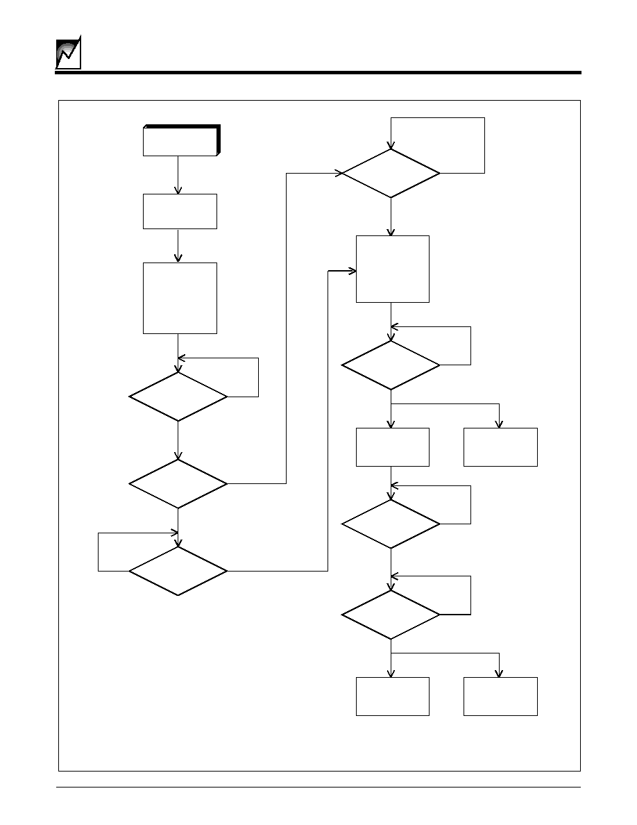
Figure 1. Sequence Flow Diagram
VCC
1V
SHUT OFF
VGATE5
VGATE3
DRVREN#
HEALTHY#
SGNL-VLD#
NO
YES
NO
YES
YES
NO
TURN ON
HEALTHY#
PCI_RST#
RELEASED?
RELEASE
RESETS
TURN ON
NO
YES
VSEL
HI ?
ASSERT
RESET
OUTPUTS
YES
HOST
3VOLT
OK?
NO
YES
HOST
5V & 3V
OK?
TURN-ON
VGATE5
VGATE3
DRVREN
START
tPURST
TIMER
NO
SGNL_VLD
BD_SEL1#
&
BD_SEL2#
CARD_5V_MON
CARD_3V_MON
tPURST
TIMEOUT?
YES
NO
2037 ILL14.2
12
SMH4042
2037 8.4 10/26/00
MEMORY OPERATION
The SMH4042 memory is configured as a 512 x 8 array.
Data are read and written via an industry standard two-
wire interface. The bus was designed for two-way, two-
line serial communication between different integrated
circuits. The two lines are a serial data line (SDA), and a
serial clock line (SCL). The SDA line must be connected
to a positive supply by a pull-up resistor, located some-
where on the bus
Input Data Protocol
The protocol defines any device that sends data onto the
bus as a "transmitter" and any device that receives data as
a "receiver." The device controlling data transmission is
called the "master" and the controlled device is called the
"slave." In all cases, the SMH4042 will be a "slave" device,
since it never initiates any data transfers.
One data bit is transferred during each clock pulse. The
data on the SDA line must remain stable during clock
HIGH time, because changes on the data line while SCL
is HIGH will be interpreted as start or stop condition.
START and STOP Conditions
When both the data and clock lines are HIGH, the bus is
said to be not busy. A HIGH-to-LOW transition on the data
line, while the clock is HIGH, is defined as the "START"
condition. A LOW-to-HIGH transition on the data line,
while the clock is HIGH, is defined as the "STOP"
condition.
Acknowledge (ACK)
Acknowledge is a software convention used to indicate
successful data transfers. The transmitting device, either
the master or the slave, will release the bus after transmit-
ting eight bits. During the ninth clock cycle, the receiver will
pull the SDA line LOW to ACKnowledge that it received
the eight bits of data.
The SMH4042 will respond with an ACKnowledge after
recognition of a START condition and its slave address
byte. If both the device and a write operation are selected,
the SMH4042 will respond with an ACKnowledge after the
receipt of each subsequent 8-bit word. In the READ mode,
the SMH4042 transmits eight bits of data, then releases
the SDA line, and monitors the line for an ACKnowledge
signal. If an ACKnowledge is detected, and no STOP
condition is generated by the master, the SMH4042 will
continue to transmit data. If an ACKnowledge is not
detected, the SMH4042 will terminate further data trans-
missions and awaits a STOP condition before returning to
the standby power mode.
Slave Address Byte
1 0 1 0
A2 A1 B0 R/W
DEVICE
IDENTIFIER
BUS
ADDRESS
2037 ILL15.0
WRITE OPERATIONS
The SMH4042 allows two types of write operations: byte
write and page write. A byte write operation writes a single
byte during the nonvolatile write period (tWR). The page
write operation allows up to 16 bytes in the same page to
be written during tWR.
Byte Write
After the slave address is sent (to identify the slave
device, and a read or write operation), a second byte is
transmitted which contains the 8 bit address of any one of
the 512 words in the array. Upon receipt of the word
address, the SMH4042 responds with an ACKnowledge.
After receiving the next byte of data, it again responds with
an ACKnowledge. The master then terminates the trans-
fer by generating a STOP condition, at which time the
SMH4042 begins the internal write cycle. While the inter-
nal write cycle is in progress, the SMH4042 inputs are
disabled, and the device will not respond to any requests
from the master.
Page Write
The SMH4042 is capable of a 16-byte page write opera-
tion. It is initiated in the same manner as the byte-write
operation, but instead of terminating the write cycle after
the first data word, the master can transmit up to 15 more
bytes of data. After the receipt of each byte, the SMH4042
will respond with an ACKnowledge.
Device Addressing
Following a start condition the master must output the
address of the slave it is accessing. The most significant
four bits of the slave address are the device type identifier
(see below). For the SMH4042 this is fixed as 1010[B].
The next two bits select one of four possible devices on
the bus. The state of the hardwired inputs (A2 and A1)
correspond to the serial bit stream A2 and A1 in the slave
address. The next bit is the block select bit, effectively the
MSB of the byte address.
Read/Write Bit
The last bit of the data stream defines the operation to be
performed. When set to "1," a read operation is selected;
when set to "0," a write operation is selected.
13
2037 8.4 10/26/00
SMH4042
The SMH4042 automatically increments the address for
subsequent data words. After the receipt of each word,
the low order address bits are internally incremented by
one. The high order bits of the address byte remain
constant. Should the master transmit more than 16 bytes,
prior to generating the STOP condition, the address
counter will "roll over," and the previously written data will
be overwritten. As with the byte-write operation, all inputs
are disabled during the internal write cycle. Refer to
Figure 5 for the address, ACKnowledge and data transfer
sequence.
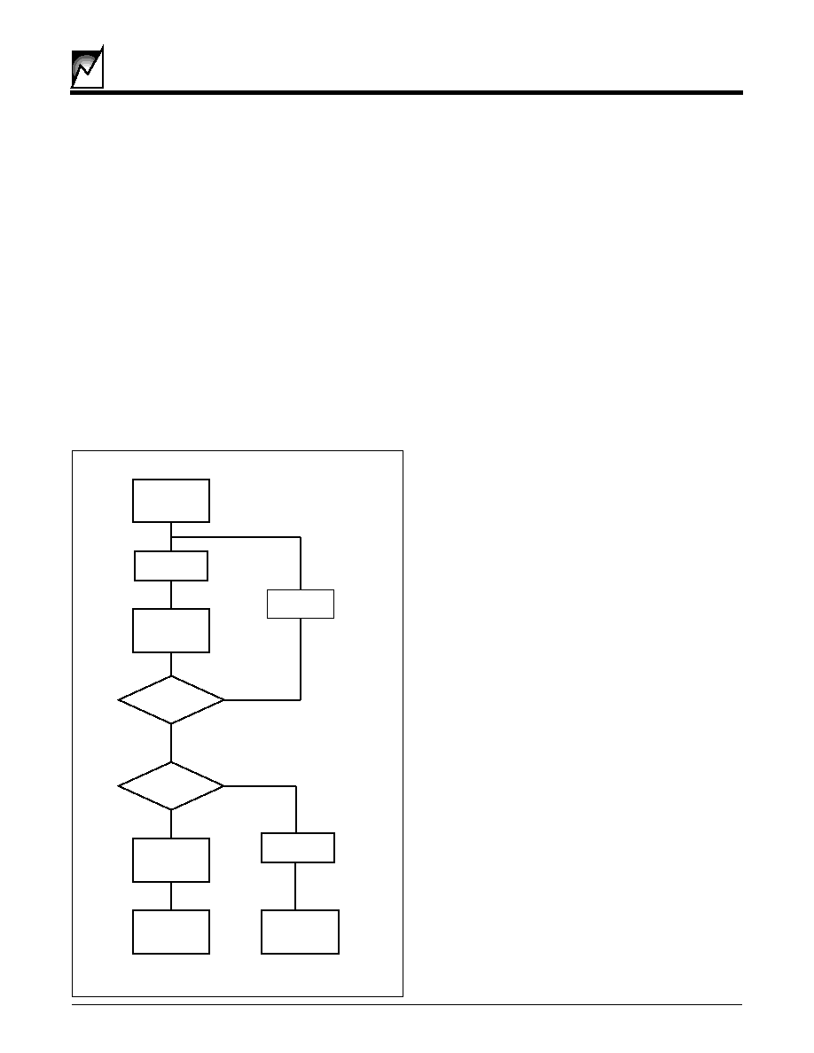
Acknowledge Polling
When the SMH4042 is performing an internal WRITE
operation, it will ignore any new START conditions. Since
the device will only return an acknowledge after it accepts
the START, the part can be continuously queried until an
acknowledge is issued, indicating that the internal WRITE
cycle is complete. See the flow diagram below for the
proper sequence of operations for polling.
Next
Operation
a Write?
ACK
Returned?
Issue
Address
Proceed
With
Write
Await
Next
Command
Issue Stop
Issue Slave
Address and
R/W = 0
Issue Stop
Issue Start
Write Cycle
In Progress
2037 ILL16.0
READ OPERATIONS
Read operations are initiated with the R/W bit of the
identification field set to "1." There are two different read
options:
1. Current Address Byte Read
2. Random Address Byte Read
Current Address Read
The SMH4042 contains an internal address counter
which maintains the address of the last word accessed,
incremented by one. If the last address accessed (either
a read or write) was to address location n, the next read
operation would access data from address location n+1
and increment the current address pointer. When the
SMH4042 receives the slave address field with the R/W
bit set to "1," it issues an acknowledge and transmits the
8-bit word stored at address location n+1. The current
address byte read operation only accesses a single byte
of data. The master does not acknowledge the transfer,
but does generate a stop condition. At this point, the
SMH4042 discontinues data transmission.
Random Address Read
Random address read operations allow the master to
access any memory location in a random fashion. This
operation involves a two-step process. First, the master
issues a write command which includes the start condition
and the slave address field (with the R/W bit set to WRITE)
followed by the address of the word it is to read. This
procedure sets the internal address counter of the
SMH4042 to the desired address. After the word address
acknowledge is received by the master, the master imme-
diately reissues a start condition followed by another
slave address field with the R/W bit set to READ. The
SMH4042 will respond with an ac-knowledge and then
transmit the 8-data bits stored at the addressed location.
At this point, the master does not acknowledge the
transmission but does generate the stop condition. The
SMH4042 discontinues data transmission and reverts to
its standby power mode.

14
SMH4042
2037 8.4 10/26/00
Sequential READ
Sequential reads can be initiated as either a current
address READ or random access READ. The first word is
transmitted as with the other byte read modes (current
address byte READ or random address byte READ);
however, the master now responds with an
ACKnowledge, indicating that it requires additional data
from the SMH4042. The SMH4042 continues to output
data for each ACKnowledge received. The master termi-
nates the sequential READ operation by not responding
with an ACKnowledge, and issues a STOP conditions.
During a sequential read operation, the internal address
counter is automatically incremented with each acknowl-
edge signal. For read operations, all address bits are
incremented, allowing the entire array to be read using a
single read command. After a count of the last memory
address, the address counter will `roll-over' and the
memory will continue to output data.
Data Download
The SMH4042 supports a proprietary mode of operation
specifically for the Hot Swap environment. After a power
on reset the internal address pointer is reset to 00. The
host or ASIC then only needs to issue a read command
and then sequentially clock out data starting at
address 00.
15
2037-07 9/23/99
SMH4042
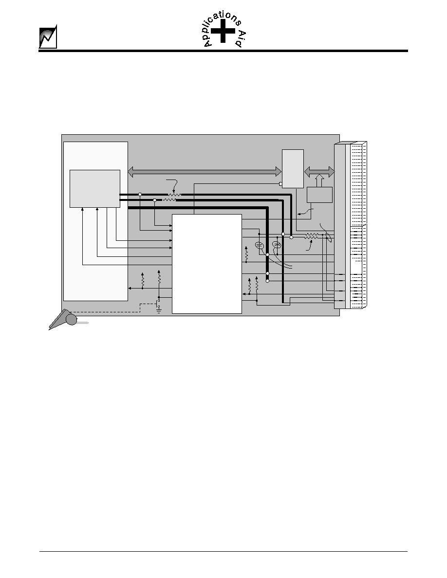
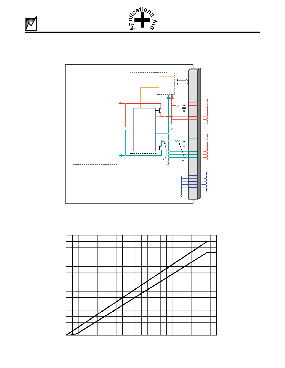
Design Considerations for a CompactPCI Board
Figure 2 is a generic representation of a CompactPCI board and it illustrates how the SMH4042 is the key component
in the board insertion/removal process. The illustrations that follow show in more detail how the various blocks interface
to the SMH4042.
Power Busses
It is important in the design of the board to insure the backend logic is isolated from the power control circuits and other
early power circuits such as FPGAs and the I/O interface circuits. In the illustration shown below, the early power
busses for +5V, +3V have series current limiting resistors. These values should be calculated so as to limit the in-rush
current that will initially charge the capacitive load of the early power circuits. As the card is inserted further, the medium
length pins engage and short out the current limiting resistors. Note the placement of the sense (shunt) resistors. They
are in series with the power-FETs and no voltage drop will be detected across the resistor until VGATE is applied to
the power-FETs. The sense resistor values are determined by dividing 50mV by the current spec for that supply.
It should be noted that there is an inherent delay from VGATE turning on to VGATE3 turning on. The typical delay is
illustrated in Figure 4.
Figure 2. Block diagram of typical
CompactPCI board.
CompactPCI Applications Aid
Backend Power Plane
and Logic
Bus
Interface
Backend Power
SwitchingCircuits
SMH4042
RESET
V(I/O)
5V
3.3V
GND
BD_SEL#
GND
GND
GND
GND
3.3V
GND, PCI_RST#
HEALTHY#
5V
+12V, -12V
P1
P2
ENUM#
CARD_3V_MON
CARD_5V_MON
VGATE3
VGATE5
PCI_RST#
GND
HST_3V_MON
VCC5
BD_SEL2#
5V
Precharge
Circuit
V(I/O)
LOCAL_PCI_RST#
Current
limiting
resistors
V(I/O)
V(I/O)
V(I/O)
eP
SGNL_VLD
eP
HEALTHY#
Capacitance
8.8
µ
f each
CBI_3
CBI_5
BD_SEL1#
1Vref
Current
sense
resistors
2037 ILL23.1
16
SMH4042
2037-07 9/23/99
CompactPCI Applications Aid
Early
Power
Early
Power
Current
Limit
Resistor
Sense
Resistor
VGATE5
VCC5
CBI_5
VGATE3
HST_3V_MON
CBI_3
CARD_3V_MON
CARD_5V_MON
Early
Power
Circuits
Backend
Power Plane
I/Os
Vref
Pre-Charge
SMH4042
Long Power Pin
Medium Power Pin
Long Power Pin
Medium Power Pin
Long Ground Pins
Medium Ground Pin
2037 ILL24.0
0V
5V
10V
15V
t0
10ms
20ms
30ms
40ms
50ms
60ms
VGATE3
VGATE5
2037 ILL25.0
Figure 3. Power Control and Power Plane Isolation
Figure 4. Typical delay between VGATE5 and VGATE3
17
2037-07 9/23/99
SMH4042
CompactPCI Applications Aid
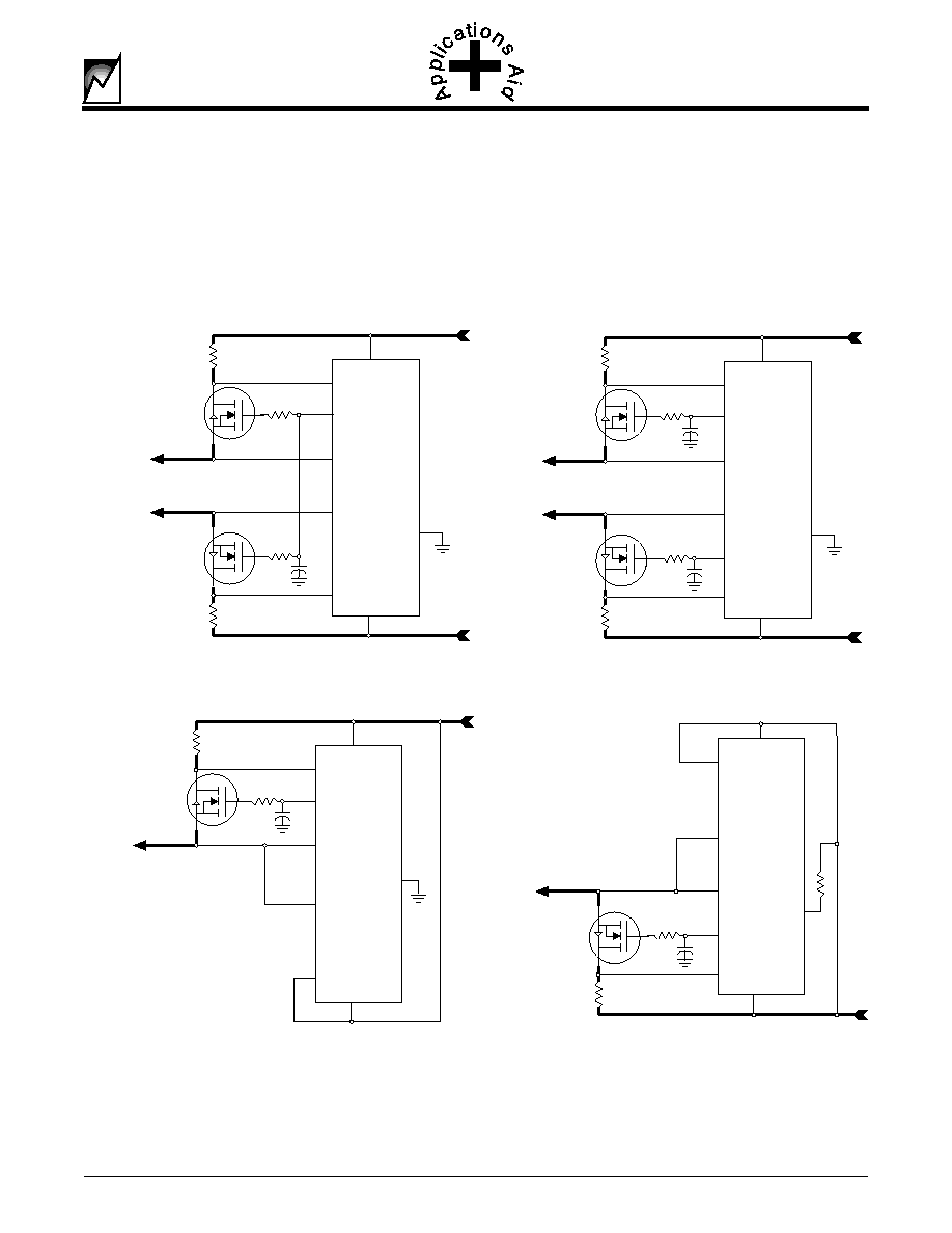
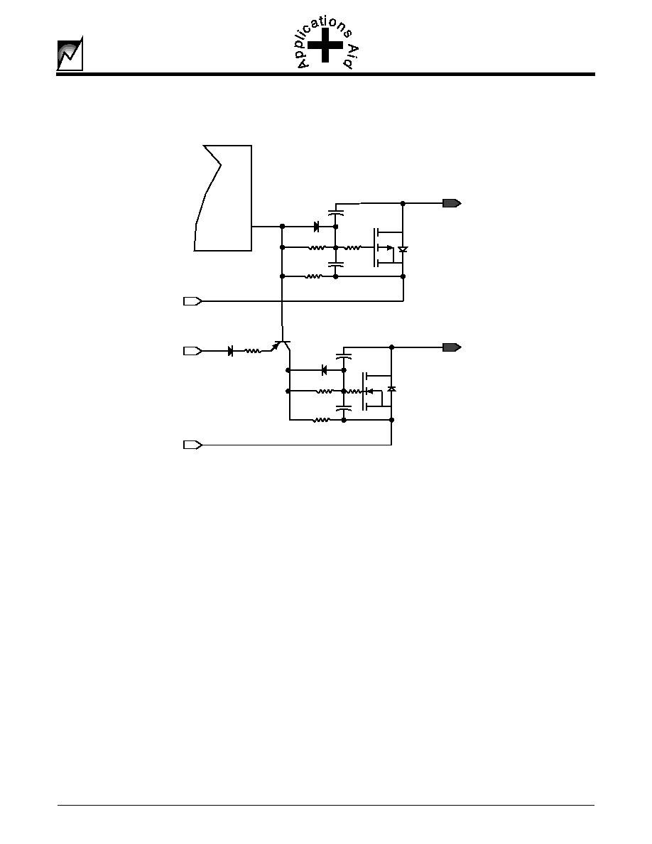
Figure 5. Four power switching implementations
Power Switching Options
The figures below illustrate four possible methods for wiring the SMH4042. In the first example both power-FETs are
connected to a single VGATE output. This should be used when the design requires the backend voltages to be
powered-up simultaneously. In the second example both VGATE outputs are being used so that the 3.3V slew lags
the 5V slew. The two bottom circuits illustrate the wiring for single power supply boards. Note how the VSEL pin is
biased differently for the two applications.
D
S
G
47nF
CARD_3V_MON
CBI_5
CARD_5V_MON
VGATE3
CBI_3
HST_3V_MON
VCC
VGATE5
+5V
±
5%
5A max
.01
VSEL
D
S
G
47nF
CARD_3V_MON
CBI_5
CARD_5V_MON
VGATE3
CBI_3
HST_3V_MON
VCC
VGATE5
+3.3V
±.3V
7.6A max
.0065
VSEL
D
S
G
D
S
G
47nF
CARD_3V_MON
CBI_5
CARD_5V_MON
VGATE3
CBI_3
HST_3V_MON
VCC
VGATE5
+5V
±
5%
5A max
+3.3V
±.3V
7.6A max
.01
.0065
VSEL
D
S
G
D
S
G
47nF
47nF
CARD_3V_MON
CBI_5
CARD_5V_MON
VGATE3
CBI_3
HST_3V_MON
VCC
VGATE5
+5V
±
5%
5A max
+3.3V ±.3V
7.6A max
.01
.0065
VSEL
Dual Voltage, Single Slew Rate Implementation
Dual Voltage, Dual Slew Rate Implementation
Single 5Volt Implementation
Single 3.3Volt Implementation
10
10
10
10
10
10
2037 Fig05 8.3
18
SMH4042
2037-07 9/23/99
CompactPCI Applications Aid
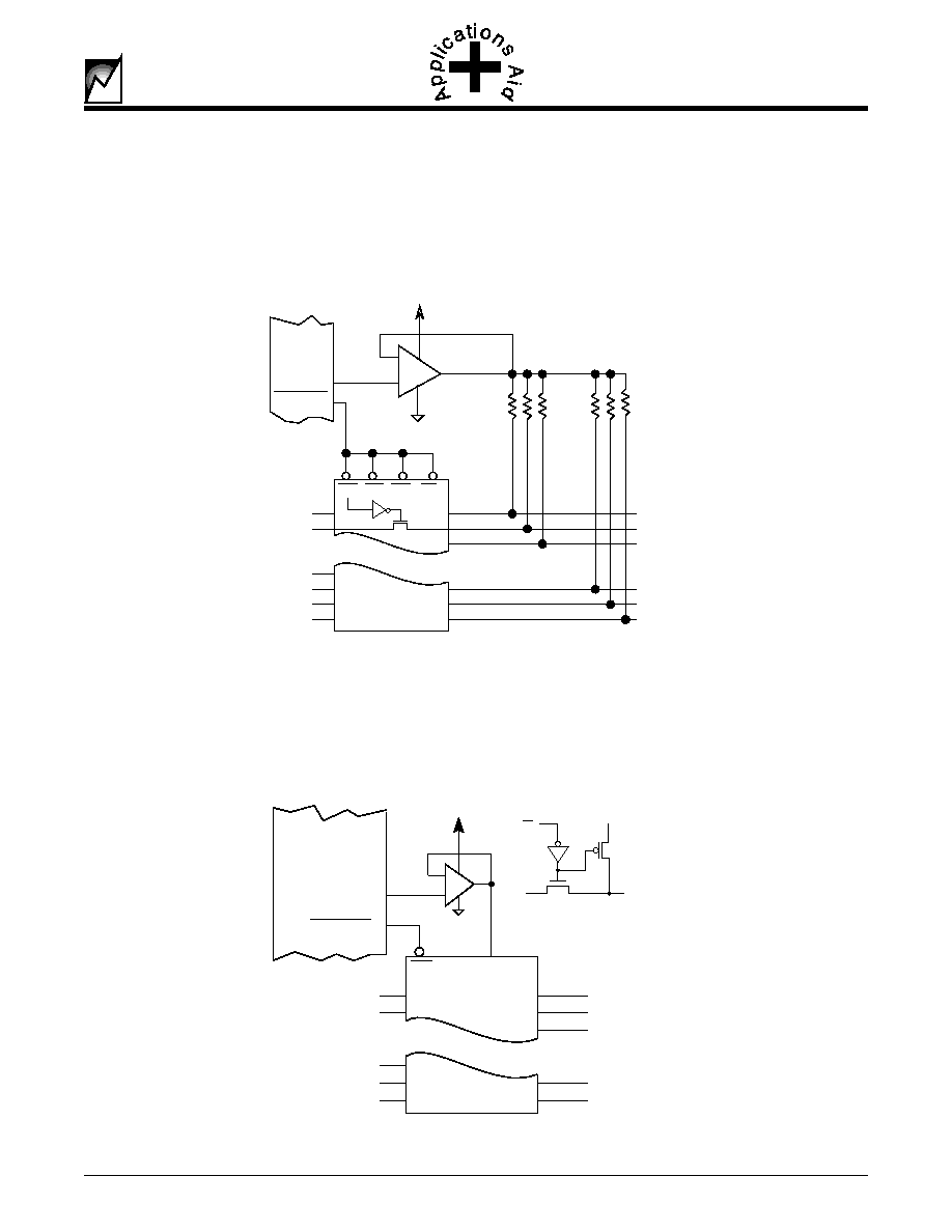
I/O Buffers
Depending upon the application requirements there are a number of silicon solutions that employ low on-resistance
CMOS switches. Figure 6 shows one implementation using a QuickSwitch
Æ
from Quality Semiconductor. This
particular device exhibits very Flat R
ON
characteristics from 0 to 5V. The only drawback is the extra space required
for the external pull-up resistors.
Figure 7 shows another implementation, but the pull-up resistor structure is incorporated in the switch. The circuit also
automatically switches the bias voltage out of the circuit as the CMOS switches are enabled. A potential advantage
is the ability to place the interface closer to the edge of the card. The board designer should evaluate their requirements
and design goals and determine their best solution. The bus switches are available from both Texas Instruments and
Pericom Semiconductor.
OE1 OE2 OE3 OE4
SGNL_VLD
A0
A1
A31
A30
A29
A28
B0
B1
B2
B30
B31
B29
QS34XVH245
HOST PCI Bus
Local PCI Bus
SMH4042
1Vref
+
-
LMV321
early power
2037 ILL27.0
ON
SGNL_VLD
A0
A1
A10
A9
A8
B0
B1
B2
B10
B9
SN74CBT6800
or PI5C6800
Host PCI Bus
Local PCI Bus
BIASV
1Vref
+
-
LMV321
Equivalent Internal
Circuit
A1
B1
ON
BIASV
2037 ILL28.0
Figure 6. Bus buffers with external pull-ups
Figure 7. Bus buffers with integrated pull-ups

19
2037-07 9/23/99
SMH4042
CompactPCI Applications Aid
I/O Pre-charge
The CompactPCI specs require the add-in board to pre-charge the board's I/Os before making contact with bus pins
and the pre-charge voltage is 1V ±0.1V. The SMH4042 provides an accurate 1volt reference output that is accurate
and stable prior to the medium length pins making contact. The 1Vref output should be the reference input to a unity
gain op amp circuit. Figure 8 is a typical implementation utilizing a common op amp.
Figure 8. I/O pre-charge circuit
Resistor Array
To/From
Backplane
To/From
Buffers or ASIC
LMV321
+
-
early power
SMH4042
1Vref
Vcc5
2037 ILL29.0
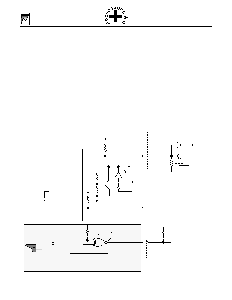
Special Considerations
The example application shown in Figure 2 shows both of the BD_SEL inputs being used independently. These two
inputs are effectively AND'ed internally and they must both be low before any sequencing will proceed. In most design
cases the BD_SEL1# connection to an injector switch is redundant and realistically can be grounded.
The CompactPCI Hot Swap spec does provide a mechanism for implementing high availability systems using "Full
Hot Swap" boards. This capability entails integrating the injector/ejector handle, the blue LED and a board status
signal. Section 2.3.2 of the
CompactPCI Hot Swap spec states the following.
∑ "A signal (ENUM#) is provided to notify the system host that either a board has been freshly inserted or is about
to be extracted."
∑ "A switch, actuated with the lower ejector handle of the board, is used to signal the insertion or impending
extraction of a board."
∑ "A blue LED, located on the from to the board is illuminated when it is permissible to extract a board."
Figure 8 illustrates a possible implementation of the circuits needed. It should be noted this will require the
implementation of a status register that works in conjunction with the switch logic to generate the ENUM# signal. Notice
the blue LED circuit and the active high reset output used to activate a current boost circuit for the LED. The sequence
of operations is as follows:
20
SMH4042
2037-07 9/23/99
CompactPCI Applications Aid
∑ The long pins engage.
∑ Power is supplied to the SMH4042, the LED and the BD_SEL" pull-up resistor.
∑ V(I/O) is either the early 5V or the early 3V, dependent upon the interface operating levels.
∑ The LED is illuminated by LOCAL_PCI_RST# going low.
∑ The medium length pins contact.
∑ The ENUM# signal should not be active at this point.
∑ The board is fully inserted and the injector switch is closed.
∑ ENUM# is driven low.
∑ BD_SEL# makes contact (optional: the pull-up on the board indicates to the host the presence of a board.)
∑ The host responds to the ENUM# signal and drives BD_SEL# low.
∑ This provides the last gating item to the SMH4042 before it will begin the power-on sequence.
V(I/O)
BD_SEL2#
V(I/O)
PRESENT
BD_SEL1#
SMH4042
Power ON
Board
Platform
RESET
LOCAL_PCI_RESET#
BD_SEL#
3.9K
10K
R
LIM
eP
PCI_RST#
PCI_RST#
eP
EIM=0
Board Status
eP
INS
EXT
Open Collector
ENUM#
LOCAL_PCI_RESET#
2037 ILL30.0
Figure 9.Full HotSwap board/host interface
Switching + and -12Volts
In some applications there may be a need to switch + or -12Volts to the backend circuits. Using the SMH4042
DRVREN# output these voltages can be controlled as shown in the Figure 9 below:
21
2037-07 9/23/99
SMH4042
CompactPCI Applications Aid
Figure 10. Using DRVREN# to switch + and -12V to the backend logic
1N4148
0.1
µ
F
0.1
µ
F
4.7K
330K
0.33
µ
F
4.7K
330K
0.33
µ
F
1N4148
+5V
eP
-12V to Backend Logic
+12V to Backend Logic
+12V
-12V
SMH4042
DRVREN#
2037 ILL31.0
10
10
22
SMH4042
2037 8.4 10/26/00
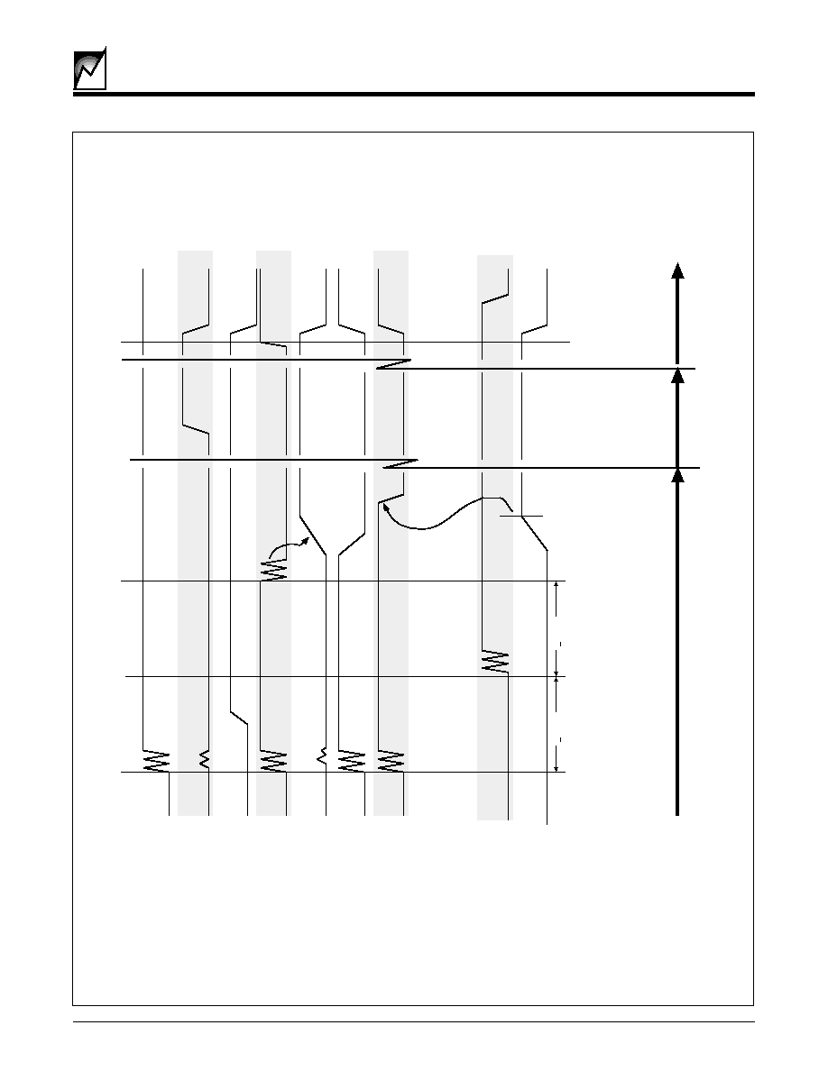
Figure 11. Typical
CompactPCI Power-on Sequence: Non-high Availability System
Ear
ly P
o
w
e
r
LOCAL_PCI_RST#
1VREF
BD_SEL#
V
G
A
TE3 &
V
G
A
TE5
DR
VREN#
HEAL
THY#
B
US _PO
WER
[mid-length pins]
BA
CKEND PO
WER
Long Pin
Mid Length Pin
Short Pin
>4ms
>4ms
Inser
tion Process
Oper
ational
Remo
v
al
(initiated b
y
BD-SEL# Disconnect)
Platf
orm
Signal
Sour
ce
SMH4042
SMH4042
Platf
orm
SMH4042
SMH4042
SMH4042
Platf
orm
HotSwap Boar
d
2037 ILL6.1
23
2037 8.4 10/26/00
SMH4042
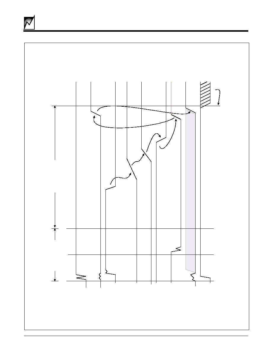
Figure 12. Power-on Sequence for a Full Hot Swap Board Using the S39421
Medium Pins
Engaged
eP
LOCAL_PCI_RST#
BD_SEL#
EJECT
OR
SWITCH
VG
A
T
E
Bac
k
end V
oltage
HEAL
THY#
PCI_RESET#
LOCAL_PCI_RESET#
LED-ON#
ENUM# OK
Platf
orm
SMH4042
System Host
SMH4042
Hot Swap
Boar
d
SMH4042
System Host
SMH4042
Hot Swap
Boar
d
Begin Softw
are
Connection Process
Long Pins
Engaged
Shor
t Pin
Engaged
Ph
ysical Connection
Hardw
are Connection
2037 ILL10.1
24
SMH4042
2037 8.4 10/26/00
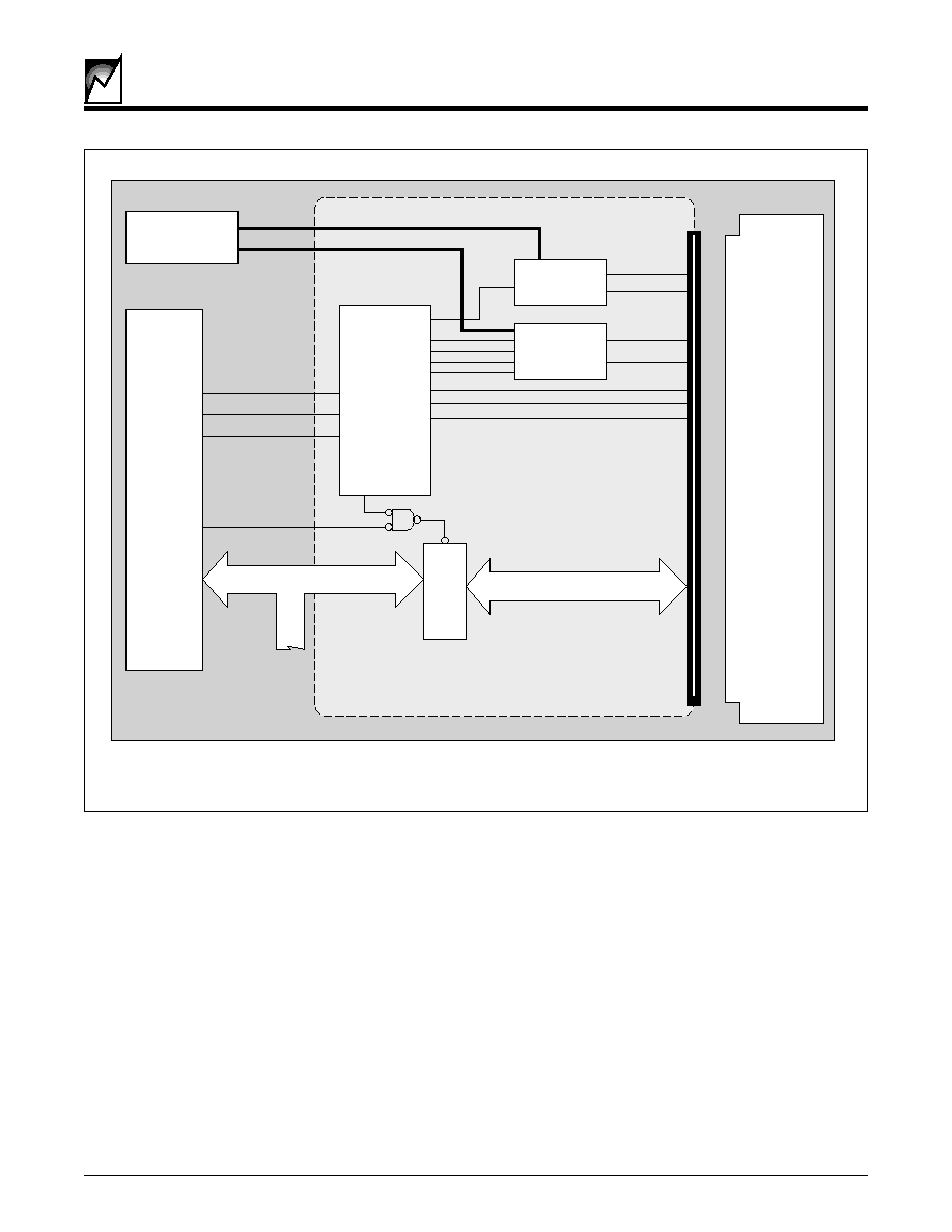
Figure 13. High Level Block Diagram Implementation for a PCI Hot Plug Slot
Although the primary application for the SMH4042 is as a
voltage controller for
CompactPCI or VME boards, it is
versatile enough to be used as a Hot Plug controller on a
host PCI card. The functional blocks are similar to those
of the
CompactPCI implementation but they are now
resident on the motherboard. The same circuits shown for
switching the voltages on the card can also be used for
controlling the slot voltages.
+12V and -12V
MOSFETs
+5V and +3V
MOSFETs
SMH4042
BUFFER
BUFFERED PCI BUS
PCI ADD-IN CARD
Power Supply
HOST LOGIC
SLOT CONTROL
FAULT#
HEALTHY#
[SGNL_VLD]
PWR_EN
PCI_RST#
VGATE3
VGATE5
CBI_3
CBI_5
CARD_3V_MON
CARD_5V_MON
LOCAL_PCI_RST#
DRVREN#
+12V
-12V
+5V
+3.3V
PCI Bus
2037 ILL22.1

25
2037 8.4 10/26/00
SMH4042
SSOP Package Drawing and Dimensions
D
0
∞
to 8
∞
typ
H
A
e
B
A
1
A
2
E
C
L
hx45
∞
1
S
JEDEC
MO-137
SSOP ILL.0
This Table in Inches
Common dimensions
Pin Count
Dimension "D"
Dimension "S"
Min
Nom
Max
Min
Nom
Max
Min
Nom
Max
A
.061
.064
.068
16
.189
.194
.196
.0020
.0045
.0070
A1
.004
.006
.0098
20
.337
.342
.344
.0500
.0525
.0550
A2
.055
.058
.061
24
.337
.342
.344
.0250
.0275
.0300
B
.008
.010
.012
28
.386
.391
.393
.0250
.0280
.0300
C
.0075
.008
.0098
D
See Variations
E
.150
.155
.157
e
.025BSC
H
.230
.236
.244
h
.010
.013
.016
L
.016
.025
.035
N
Pin Count
S
See Variations
This Table in Millimeters
Common dimensions
Pin Count
Dimension "D"
Dimension "S"
Min
Nom
Max
Min
Nom
Max
Min
Nom
Max
A
1.55
1.63
1.73
16
4.80
4.93
4.98
0.05
0.11
0.18
A1
0.12
0.15
0.25
20
8.56
8.69
8.74
1.27
1.33
1.40
A2
1.40
1.47
1.55
24
8.56
8.69
8.74
0.64
0.70
0.76
B
0.20
0.25
0.31
28
9.80
9.93
9.98
0.64
0.71
0.76
C
0.19
0.20
0.25
D
See Variations
E
3.81
3.94
3.99
e
0.635 BSC
H
5.84
5.99
6.20
h
0.25
0.33
0.41
L
0.41
0.64
0.89
N
Pin Count
S
See Variations
26
SMH4042
2037 8.4 10/26/00
28-Lead Small Outline Package (SOIC)
0.014 - 0.019
(0.356 - 0.482)
0.004 - 0.012
(0.102 - 0.305)
0.037 - 0.045
(0.940 - 1.143
0.701 - 0.711*
(17.01 - 18.06)
0.394 - 0.419
(10.00 - 10.65)
0.093 - 0.104
(2.362 - 2.642)
0.016 - 0.050
(0.406 - 1.270)
0.050
(1.270)
0.009 - 0.013
(0.229 - 0.330)
0.010 - 0.029
(0.254 - 0.737)
0.291 - 0.299
(7.391 - 7.595)
x45
∞
0
∞
to 8
∞
typ
28pn SOIC ILL.1
27
2037 8.4 10/26/00
SMH4042
ORDERING INFORMATION
A
SMH4042
Base Part Number
Offset
M = 50mV over
N = 50mV under
VTRIP2
G
H
K
L
VTRIP1
A
B
Package Style
G = 28 Lead SSOP
S = 28 Lead SOIC
G
G M
2037 ILL17.3
Package
Vtrip1
Vtrip2
Offset
S
A
G
M
S
A
G
N
S
A
H
M
S
A
H
N
S
A
K
M
S
A
K
N
S
B
G
M
S
B
G
N
S
B
H
M
S
B
H
N
S
B
K
M
S
B
K
N
S
B
L
M
S
B
L
N
Package
Vtrip1
Vtrip2
Offset
G
A
G
M
G
A
G
N
G
A
H
M
G
A
H
N
G
A
K
M
G
A
K
N
G
B
G
M
G
B
G
N
G
B
H
M
G
B
H
N
G
B
K
M
G
B
K
N
G
B
L
M
G
B
L
N
Note: Contact the factory for information regarding "AL" Vtrip availability.
VALID ORDERING COMBINATIONS
28
SMH4042
2037 8.4 10/26/00
NOTICE
SUMMIT Microelectronics, Inc. reserves the right to make changes to the products contained in this publication
in order to improve design, performance or reliability. SUMMIT Microelectronics, Inc. assumes no responsibility
for the use of any circuits described herein, conveys no license under any patent or other right, and makes no
representation that the circuits are free of patent infringement. Charts and schedules contained herein reflect
representative operating parameters, and may vary depending upon a user's specific application. While the
information in this publication has been carefully checked, SUMMIT Microelectronics, Inc. shall not be liable for any
damages arising as a result of any error or omission.
SUMMIT Microelectronics, Inc. does not recommend the use of any of its products in life support or aviation
applications where the failure or malfunction of the product can reasonably be expected to cause any failure of
either system or to significantly affect their safety or effectiveness. Products are not authorized for use in such
applications unless SUMMIT Microelectronics, Inc. receives written assurances, to its satisfaction, that: (a) the risk
of injury or damage has been minimized; (b) the user assumes all such risks; and (c) potential liability of SUMMIT
Microelectronics, Inc. is adequately protected under the circumstances.
HotSwapTM is a trademark of Summit Microelectronics, Inc.
PICMGTM & CompactPCITM are trademarks of PCI Industrial Computer Manufacturers' Group.
I
2
CTM is a trademark of Philips Corporation.