 | –≠–ª–µ–∫—Ç—Ä–æ–Ω–Ω—ã–π –∫–æ–º–ø–æ–Ω–µ–Ω—Ç: SMH4802G | –°–∫–∞—á–∞—Ç—å:  PDF PDF  ZIP ZIP |
Characteristics subject to change without notice
2062 2.3 6/19/03
SMH4802
SUMMIT
MICROELECTRONICS, Inc.
©SUMMIT MICROELECTRONICS, Inc., 2003
∑
1717 Fox Drive
∑
San Jose, CA 95131
∑
Phone 408-436-9890
∑
FAX 408-436-9897
∑
www.summitmicro.com
Preliminary Information
See Last Page
Programmable -48V Hot-Swap Controller with Forced Shut Down
FEATURES & APPLICATIONS
SIMPLIFIED APPLICATION DRAWING
l Soft Start Power Supply
l Live Insertion into a -48V backplane
l Programmable Control of a DC/DC Converter
w I
2
C Power On/Off Control
l Highly Programmable Circuit Breaker
w Active In-rush Current Limiting
w Over-current Filter Circuit Breaker Immunity
to Voltage Steps and Current Spikes
l Programmable Forced Shutdown Timer
l Internal Shunt Regulator Allows a Wide Supply
Range
l 14-pin SOIC and 16-pin SSOP packages
APPLICATIONS
l -48V Power Distribution
w Telecom Line Cards
w Central Office Switching
w High Availability Servers
w Hot Board Insertion
The SMH4802 is designed to control in-rush current
during hot swapping of plug-in cards operating in a
distributed power environment. The device drives an
external power MOSFET switch that connects the supply
to the load and protects against over-current conditions
that might disrupt the host supply. It also provides under-
voltage and over-voltage monitoring of the host power
supply. When the source and drain voltages of the
external MOSFETs are within specification it will provide
a Power Good logic output that can be used to enable a
DC/DC converter. Additional features of the device
include: temperature sense or master enable input, a 5V
reference output for expanding monitor functions, and
duty-cycle or latched over-current protection modes. An
internal Shunt regulator allows a wide supply range. The
SMH4802 -48V Hot-Swap Controller also features a
simple software I
2
C Power On/Off Interface for remote
power control applications.
Programming of configuration, control and calibration val-
ues by the user can be simplified with the SMX3200
interface adapter and a windows based GUI supplied by
Summit.
INTRODUCTION
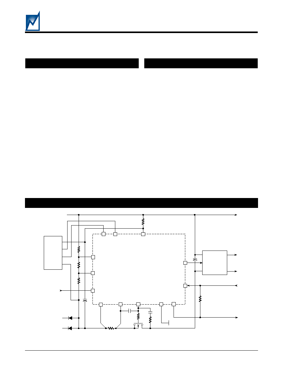
Figure 1. The drawing illustrates the SMH4802 in a typical line-card application. It should be noted this is just an
example, and the specific component values are purposely not shown. Pin numbers reflect SOIC package.
V
DD
UV
OV
PG#
5VREF
2062 SAD
≠48V Ret
≠48V B
SDA
SCL
DC/DC
SMH4802
FS#
DRAIN
SENSE
14
5
4
10
12
9
8
11
1
≠48V A
I
2
C
Header
R
D
EN/TS
3
V+
V≠
Out≠
Out+
On/
Off
VSS
CBSENSE
VGATE
6
7
2
R
S
V
SS
2
SMH4802
2062 2.3 6/19/03
SUMMIT MICROELECTRONICS, Inc.
Preliminary Information
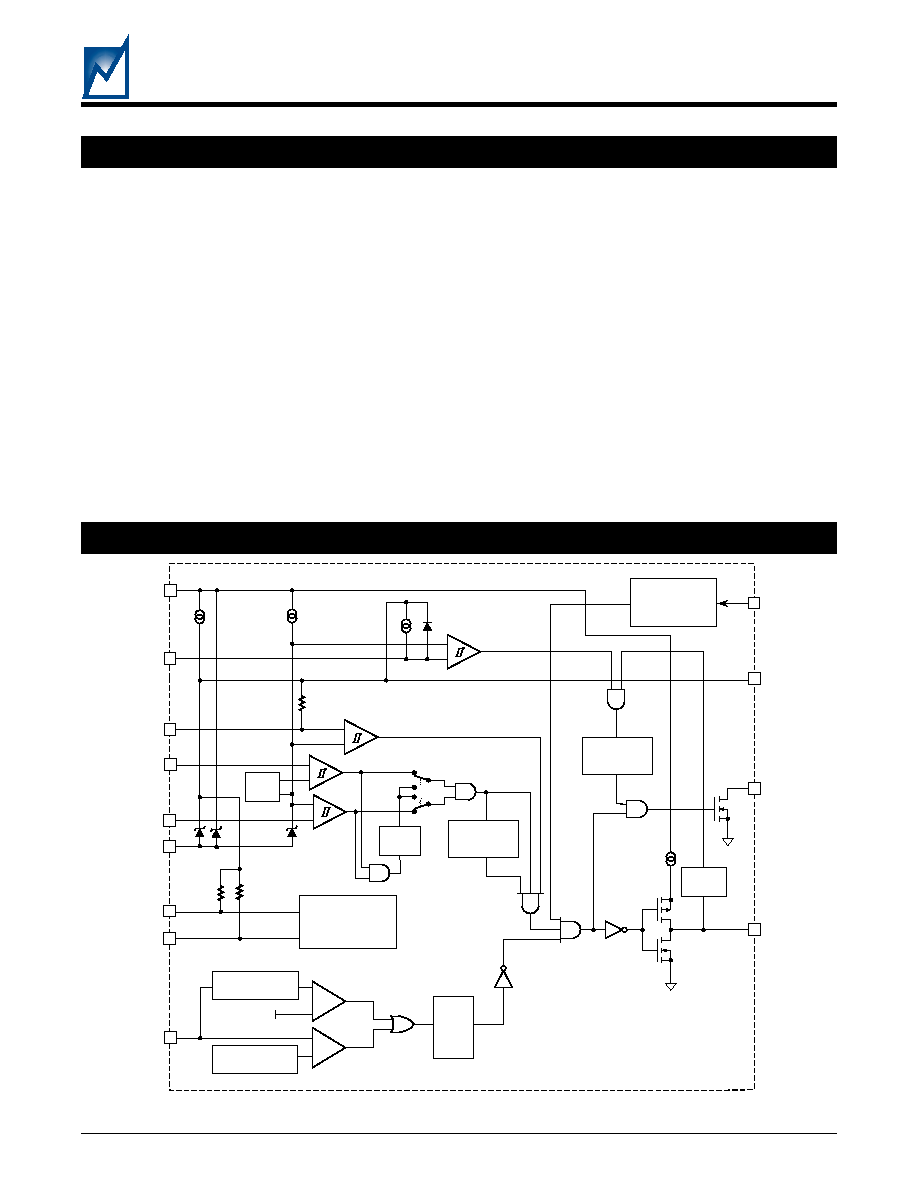
FUNCTIONAL BLOCK DIAGRAM
The SMH4802 is an integrated power controller for hot
swappable add-in cards. The device operates from a wide
supply range and generates the signals necessary to
drive an isolated output DC/DC converter. As a typical
add-in board is inserted into the powered backplane,
physical connections must first be made with the chassis
to discharge any electrostatic voltage potentials. The
board then contacts the long pins on the backplane that
provide power and ground. As soon as power is applied,
the device starts up, but does not immediately apply
power to the output load. Under-voltage and over-voltage
circuits inside the controller verify the input voltage is
within the user-specified range.
Once these requirements are met, the hot-swap controller
enables VGATE to turn on the external power MOSFET.
The VGATE output is current limited to I
VGATE,
allowing the
slew rate to be easily modified using external passive
GENERAL DESCRIPTION
components. During the controlled turn-on period the V
DS
of the MOSFET is monitored by the DRAIN SENSE input.
When DRAIN SENSE drops below 2.5V, and VGATE is
greater than V
DD
≠ V
GT
, the PG# output can begin turning
on the DC/DC converter.
Steady state operation is maintained as long as all
conditions are normal. Any of the following events may
cause the device to disable the DC/DC controller by
shutting down the power MOSFET: an under-voltage or
over-voltage condition on the host power supply; an over-
current event detected on the CBSENSE input; a failure
of the power MOSFET sensed via the DRAIN SENSE pin;
the master enable (EN/TS) falling below 2.5V; or the FS#
input being driven low by events on the secondary side of
the DC/DC controller. If one of these events occurs the
SMH4802 can be configured so VGATE shuts off and
either latches into an off state or recycles power after a
cooling down period, t
CYC
.
Figure 2. Functional Block diagram.
Pin numbers reflect SOIC package.
PROGRAMMED
DELAY
PROGRAMM-
ABLE
DELAY
+
≠
+
≠
+
≠
PROGRAMMED
Quick-Trip
50mV
DUTY
CYCLE
TIMER
+
≠
+
≠
5V
2.5V
12V
VGATE
SENSE
+
≠
VDD
VSS
CBSENSE
EN/TS
SCL
SDA
UV
OV
PG#
DRAIN
SENSE
VGATE
5.0VREF
12VREF
2062 BD
PROGRAMMABLE
SHUTDOWN
TIMER
FS#
14
3
1
5
9
7
4
8
6
2
11
12
10
200k
I2C INTERFACE
LOGIC
50k
50k
PROGRAMM-
ABLE
DELAY
OV/UV
FILTER
Prog.
Ref.
3
2062 2.3 6/19/03
SMH4802
SUMMIT MICROELECTRONICS, Inc.
Preliminary Information
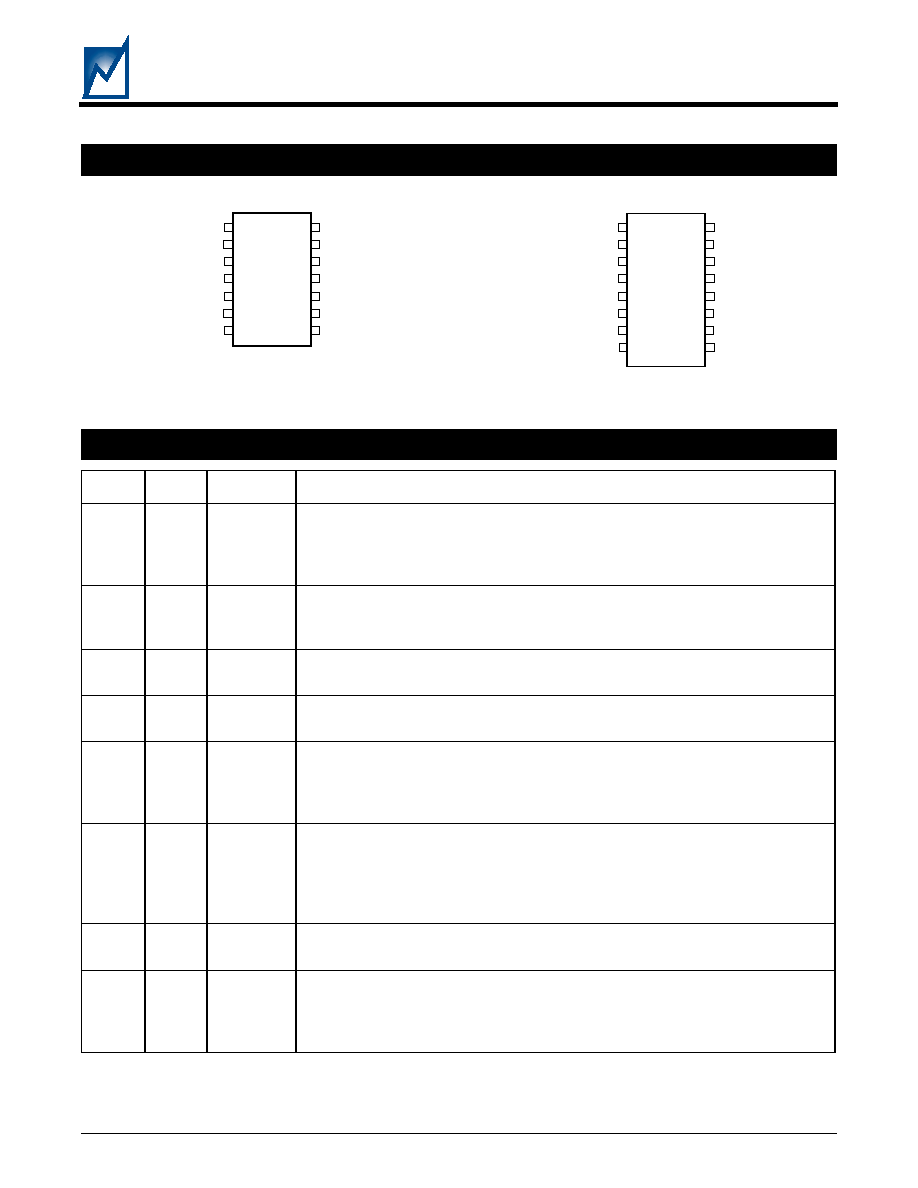
PIN CONFIGURATION
PIN DESCRIPTIONS
2062 Pin Table A
DRAIN SENSE
VGATE
EN/TS
SDA
SCL
CBSENSE
V
SS
V
DD
nc
PG#
5VREF
FS#
OV
UV
1
2
3
4
5
6
7
14
13
12
11
10
9
8
2062 14 PCon
14-Pin SOIC
Note: Pin numbers reflect the 14 Pin SOIC package.
DRAIN SENSE
VGATE
EN/TS
nc
SDA
SCL
CBSENSE
V
SS
V
DD
nc
PG#
nc
5VREF
FS#
OV
UV
1
2
3
4
5
6
7
8
16
15
14
13
12
11
10
9
2062 16 PCon
16-Pin SSOP
.
o
N
n
i
P
e
p
y
T
e
m
a
N
n
i
P
n
o
i
t
p
i
r
c
s
e
D
n
i
P
1
I
N
I
A
R
D
E
S
N
E
S
e
h
t
(
T
E
F
S
O
M
e
h
t
f
o
n
i
a
r
d
e
h
t
t
a
e
g
a
t
l
o
v
e
h
t
s
r
o
t
i
n
o
m
t
u
p
n
i
E
S
N
E
S
N
I
A
R
D
e
h
T
V
o
t
t
c
e
p
s
e
r
h
t
i
w
s
i
e
r
u
s
a
e
m
S
S
0
1
l
a
n
r
e
t
n
i
n
A
.
)
µ
N
I
A
R
D
e
h
t
s
l
l
u
p
e
c
r
u
o
s
A
w
o
l
e
b
d
l
e
h
e
b
t
s
u
m
E
S
N
E
S
N
I
A
R
D
.
l
e
v
e
l
F
E
R
V
5
e
h
t
s
d
r
a
w
o
t
l
a
n
g
i
s
E
S
N
E
S
.
t
u
p
t
u
o
#
G
P
e
h
t
e
l
b
a
n
e
o
t
V
5
.
2
2
O
E
T
A
G
V
V
o
t
l
a
u
q
e
y
l
r
a
e
n
,
t
u
p
t
u
o
e
v
i
r
d
e
d
i
s
h
g
i
h
a
s
i
t
u
p
t
u
o
E
T
A
G
V
e
h
T
D
D
n
r
u
t
o
t
d
e
s
u
,
t
u
p
t
u
o
t
n
e
r
r
u
c
t
n
a
t
s
n
o
c
a
s
e
i
l
p
p
u
s
l
a
n
g
i
s
s
i
h
T
.
T
E
F
S
O
M
r
e
w
o
p
l
a
n
r
e
t
x
e
n
a
n
o
0
0
1
(
µ
.
e
t
a
r
w
e
l
s
n
o
-
n
r
u
t
T
E
F
S
O
M
e
h
t
f
o
t
n
e
m
t
s
u
j
d
a
y
s
a
e
s
w
o
l
l
a
h
c
i
h
w
)
l
a
c
i
p
y
t
A
3
I
S
T
/
N
E
e
b
l
l
i
w
E
T
A
G
V
.
t
u
p
n
i
e
l
b
a
n
e
r
e
t
s
a
m
e
h
t
s
i
t
u
p
n
i
e
s
n
e
S
e
r
u
t
a
r
e
p
m
e
T
/
e
l
b
a
N
E
e
h
T
k
0
0
2
l
a
n
r
e
t
n
i
n
a
s
a
h
n
i
p
s
i
h
T
.
V
5
.
2
n
a
h
t
s
s
e
l
s
i
S
T
/
N
E
f
i
d
e
l
b
a
s
i
d
.
V
5
o
t
p
u
l
l
u
p
4
O
/
I
A
D
S
.
t
u
p
t
u
o
n
i
a
r
d
n
e
p
o
n
a
s
a
d
e
r
u
g
i
f
n
o
c
s
i
t
I
.
n
i
p
a
t
a
d
l
a
i
r
e
s
l
a
n
o
i
t
c
e
r
i
d
i
b
e
h
t
s
i
A
D
S
k
0
5
l
a
n
r
e
t
n
i
n
a
s
i
e
r
e
h
T
.
F
E
R
V
5
o
t
d
e
t
c
e
n
n
o
c
r
o
t
s
i
s
e
r
5
I
L
C
S
n
I
.
s
r
e
t
s
i
g
e
r
n
o
i
t
a
r
u
g
i
f
n
o
c
e
h
t
f
o
t
u
o
d
n
a
o
t
n
i
a
t
a
d
k
c
o
l
c
o
t
d
e
s
u
s
i
t
u
p
n
i
L
C
S
e
h
T
d
a
e
r
e
h
t
n
I
.
H
G
I
H
s
i
L
C
S
e
l
i
h
w
A
D
S
n
o
e
l
b
a
t
s
n
i
a
m
e
r
t
s
u
m
a
t
a
d
e
d
o
m
e
t
i
r
w
e
h
t
k
0
5
l
a
n
r
e
t
n
i
n
a
s
i
e
r
e
h
T
.
L
C
S
f
o
e
g
d
e
g
n
i
l
l
a
f
e
h
t
n
o
t
u
o
d
e
k
c
o
l
c
s
i
a
t
a
d
e
d
o
m
.
F
E
R
V
5
o
t
d
e
t
c
e
n
n
o
c
r
o
t
s
i
s
e
r
6
I
E
S
N
E
S
B
C
s
s
o
r
c
a
s
n
o
i
t
i
d
n
o
c
t
n
e
r
r
u
c
-
r
e
v
o
t
c
e
t
e
d
o
t
d
e
s
u
s
i
t
u
p
n
i
E
S
N
E
S
r
e
k
a
e
r
B
t
i
u
c
r
i
C
e
h
T
R
(
r
o
t
s
i
s
e
r
e
s
n
e
s
e
u
l
a
v
w
o
l
,
l
a
n
r
e
t
x
e
n
a
S
.
T
E
F
S
O
M
r
e
w
o
p
e
h
t
h
t
i
w
s
e
i
r
e
s
n
i
d
e
i
t
)
t
n
a
h
t
r
e
g
n
o
l
r
o
f
r
o
t
s
i
s
e
r
e
h
t
s
s
o
r
c
a
V
m
0
5
n
a
h
t
r
e
t
a
e
r
g
f
o
p
o
r
d
e
g
a
t
l
o
v
A
D
B
C
l
l
i
w
V
o
t
y
l
t
c
e
r
i
d
n
i
p
e
h
t
t
c
e
n
n
o
c
E
S
N
E
S
B
C
e
l
b
a
s
i
d
o
T
.
r
e
k
a
e
r
b
t
i
u
c
r
i
c
e
h
t
p
i
r
t
S
S
A
.
.
e
l
b
a
l
i
a
v
a
o
s
l
a
s
i
t
n
i
o
p
e
s
n
e
s
p
i
r
T
-
k
c
i
u
Q
e
l
b
a
m
m
a
r
g
o
r
p
7
R
W
P
V
S
S
V
S
S
F
E
R
V
5
e
h
t
d
n
a
s
t
u
p
n
i
l
l
A
.
y
l
p
p
u
s
e
h
t
f
o
e
d
i
s
e
v
i
t
a
g
e
n
,
e
h
t
o
t
d
e
t
c
e
n
n
o
c
s
i
V
o
t
d
e
c
n
e
r
e
f
e
r
e
r
a
t
u
p
t
u
o
S
S
.
8
I
V
U
n
o
i
t
c
n
u
j
n
o
c
n
i
y
l
l
a
c
i
p
y
t
,
r
o
t
i
n
o
m
y
l
p
p
u
s
e
g
a
t
l
o
v
-
r
e
d
n
u
n
a
s
a
d
e
s
u
s
i
n
i
p
V
U
e
h
T
.
V
5
.
2
n
a
h
t
s
s
e
l
s
i
V
U
f
i
d
e
l
b
a
s
i
d
e
b
l
l
i
w
E
T
A
G
V
.
r
e
d
d
a
l
r
o
t
s
i
s
e
r
l
a
n
r
e
t
x
e
n
a
h
t
i
w
n
i
e
l
b
a
t
s
u
j
d
a
,
t
u
p
n
i
V
U
e
h
t
n
o
e
l
b
a
l
i
a
v
a
s
i
s
i
s
e
r
e
t
s
y
h
l
a
n
r
e
t
n
i
e
l
b
a
m
m
a
r
g
o
r
p
A
.
t
u
p
n
i
V
U
e
h
t
n
o
e
l
b
a
l
i
a
v
a
o
s
l
a
s
i
y
a
l
e
d
r
e
t
l
i
f
A
.
V
m
5
.
2
6
f
o
s
t
n
e
m
e
r
c
n
i

4
SMH4802
2062 2.3 6/19/03
SUMMIT MICROELECTRONICS, Inc.
Preliminary Information
PIN DESCRIPTIONS (
Continued
)
2062 Pin Table B
Note: Pin numbers reflect the 14 Pin SOIC package.
.
o
N
n
i
P
e
p
y
T
e
m
a
N
n
i
P
n
o
i
t
p
i
r
c
s
e
D
n
i
P
9
I
V
O
n
o
i
t
c
n
u
j
n
o
c
n
i
y
l
l
a
c
i
p
y
t
,
r
o
t
i
n
o
m
y
l
p
p
u
s
e
g
a
t
l
o
v
-
r
e
d
n
u
n
a
s
a
d
e
s
u
s
i
n
i
p
V
O
e
h
T
n
a
h
t
r
e
t
a
e
r
g
s
i
V
O
f
i
d
e
l
b
a
s
i
d
e
b
l
l
i
w
E
T
A
G
V
.
r
e
d
d
a
l
r
o
t
s
i
s
e
r
l
a
n
r
e
t
x
e
n
a
h
t
i
w
.
t
u
p
n
i
V
O
e
h
t
n
o
e
l
b
a
l
i
a
v
a
o
s
l
a
s
i
y
a
l
e
d
r
e
t
l
i
f
A
.
V
5
.
2
0
1
I
#
S
F
#
G
P
e
h
t
d
n
a
E
T
A
G
V
s
e
s
u
a
c
t
a
h
t
t
u
p
n
i
w
o
l
e
v
i
t
c
a
n
a
s
i
n
i
p
n
w
o
d
t
u
h
S
d
e
c
r
o
F
e
h
T
.
d
e
r
i
p
x
e
s
a
h
r
e
m
i
t
f
f
o
-
d
l
o
h
l
a
n
r
e
t
n
i
n
a
r
e
t
f
a
e
m
i
t
y
n
a
t
a
n
w
o
d
t
u
h
s
e
b
o
t
t
u
p
t
u
o
e
r
a
h
c
i
h
w
(
e
d
i
s
y
r
a
d
n
o
c
e
s
e
h
t
n
o
s
t
i
u
c
r
i
c
y
r
o
s
i
v
r
e
p
u
s
s
w
o
l
l
a
r
e
m
i
t
f
f
o
-
d
l
o
h
e
h
T
-
o
t
p
o
n
a
a
i
v
2
0
8
4
H
M
S
e
h
t
f
o
n
w
o
d
t
u
h
s
l
o
r
t
n
o
c
o
t
)
y
l
l
a
i
t
i
n
i
p
u
d
e
r
e
w
o
p
t
o
n
.
r
o
t
s
i
s
e
r
p
u
l
l
u
p
o
n
s
a
h
t
u
p
n
i
s
i
h
T
.
r
o
t
a
l
o
s
i
1
1
O
F
E
R
V
5
t
u
p
n
i
c
i
g
o
l
e
h
t
d
n
a
p
x
e
o
t
d
e
s
u
e
b
y
a
m
t
a
h
t
e
g
a
t
l
o
v
e
c
n
e
r
e
f
e
r
t
u
p
t
u
o
V
5
a
s
i
s
i
h
T
V
o
t
t
c
e
p
s
e
r
h
t
i
w
s
i
t
u
p
t
u
o
e
c
n
e
r
e
f
e
r
e
h
T
.
2
0
8
4
H
M
S
e
h
t
n
o
s
n
o
i
t
c
n
u
f
S
S
.
2
1
O
#
G
P
e
b
n
a
c
t
I
.
r
o
t
s
i
s
e
r
p
u
l
l
u
p
l
a
n
r
e
t
n
i
o
n
h
t
i
w
t
u
p
t
u
o
w
o
l
-
e
v
i
t
c
a
,
n
i
a
r
d
-
n
e
p
o
n
a
s
i
#
G
P
3
r
e
t
f
a
d
e
l
b
a
n
e
s
i
#
G
P
.
r
e
t
r
e
v
n
o
c
C
D
/
C
D
a
e
l
b
a
n
e
r
o
d
a
o
I
a
h
c
t
i
w
s
o
t
d
e
s
u
V
s
e
h
c
a
e
r
E
T
A
G
V
:
s
t
n
e
v
e
D
D
V
-
T
G
,
V
5
.
2
n
a
h
t
s
s
e
l
s
i
e
g
a
t
l
o
v
e
s
n
e
S
n
i
a
r
D
e
h
t
,
d
e
e
c
x
e
t
o
n
n
a
c
n
i
p
s
i
h
t
n
o
e
g
a
t
l
o
V
.
d
e
r
i
p
x
e
s
a
h
e
m
i
t
y
a
l
e
d
d
e
m
m
a
r
g
o
r
p
e
h
t
d
n
a
V
o
t
d
e
c
n
e
r
e
f
e
r
s
a
V
2
1
S
S
.
3
1
c
n
c
n
n
o
i
t
c
e
n
n
o
c
o
N
4
1
R
W
P
V
D
D
V
D
D
d
e
t
c
e
n
n
o
c
r
o
t
a
l
u
g
e
r
t
n
u
h
s
l
a
n
r
e
t
n
i
n
A
.
n
o
i
t
c
e
n
n
o
c
y
l
p
p
u
s
e
v
i
t
i
s
o
p
e
h
t
s
i
V
n
e
e
w
t
e
b
D
D
V
d
n
a
S
S
.
2
0
8
4
H
M
S
e
h
t
s
e
i
l
p
p
u
s
t
a
h
t
V
2
1
y
l
e
t
a
m
i
x
o
r
p
p
a
s
p
o
l
e
v
e
d
V
e
h
t
h
t
i
w
s
e
i
r
e
s
n
i
d
e
c
a
l
p
e
b
t
s
u
M
r
o
t
s
i
s
e
r
A
D
D
t
n
e
r
r
u
c
r
o
t
a
l
u
g
e
r
e
h
t
t
i
m
i
l
o
t
n
i
p
R
(
D
.
)
s
n
o
i
t
a
r
t
s
u
l
l
i
n
o
i
t
a
c
i
l
p
p
a
e
h
t
n
i
5
2062 2.3 6/19/03
SMH4802
SUMMIT MICROELECTRONICS, Inc.
Preliminary Information
Temperature Range ............ (Industrial) ≠40∞C to 85∞C
.......................................... (Commercial) ≠5∞C to 70∞C
T
J(Max)
................................................................ 150∞C
R
J-A
..................................... *
Q 88∞C/W; R 115∞C/W
R
J-C
....................................... *
Q 37∞C/W; R 40∞C/W
Note -- The device is not guaranteed to function outside its operating
rating. Stresses listed under Absolute Maximum Ratings may cause
permanent damage to the device. These are stress ratings only, and
functional operation of the device at these or any other conditions outside
those listed in the operational sections of this specification is not implied.
Exposure to any absolute maximum rating for extended periods may
affect device performance and reliability.
*
Q 14 pin SOIC; R 16 pin SSOP.
Temperature Under Bias ..................... ≠55∞C to 125∞C
Storage Temperature .......................... ≠65∞C to 150∞C
Lead Solder Temperature (10 secs) .................. 300∞C
Terminal Voltage with Respect to V
SS
:
V
DD
............................................. ≠0.5V to V
DD
OV, UV, DRAIN SENSE, SCL, SDA, FS#,
CBSENSE ........................ ≠0.5V to V
DD
+0.5V
EN/TS ....................................................... 10V
PG# .................................. ≠0.5V to V
DD
+0.5V
VGATE ........................................... V
DD
+0.5V
ABSOLUTE MAXIMUM RATINGS*
RECOMMENDED OPERATING CONDITIONS
DC OPERATING CHARACTERISTICS
(Over Recommended Operating Conditions; Voltages are relative to V
SS
, except V
GT
)
2062 Elect Table
l
o
b
m
y
S
r
e
t
e
m
a
r
a
P
s
n
o
i
t
i
d
n
o
C
.
n
i
M
.
p
y
T
.
x
a
M
s
t
i
n
U
V
D
D
e
g
a
t
l
o
v
y
l
p
p
u
S
I
D
D
A
m
3
=
1
1
2
1
3
1
V
V
5
F
E
R
t
u
p
t
u
o
e
c
n
e
r
e
f
e
r
V
5
I
D
D
A
m
3
=
5
7
.
4
0
0
.
5
5
2
.
5
V
I
5
D
A
O
L
t
n
e
r
r
u
c
t
u
p
t
u
o
e
c
n
e
r
e
f
e
r
V
5
I
D
D
A
m
3
=
1
≠
1
A
m
I
D
D
t
n
e
r
r
u
c
y
l
p
p
u
s
r
e
w
o
P
2
0
1
A
m
V
V
U
d
l
o
h
s
e
r
h
t
e
g
a
t
l
o
V
-
r
e
d
n
U
I
D
D
A
m
3
=
5
7
4
.
2
0
0
5
.
2
5
2
5
.
2
V
V
T
S
Y
H
V
U
s
i
s
e
r
e
t
s
y
h
e
g
a
t
l
o
V
-
r
e
d
n
U
I
D
D
A
m
3
=
3
6
V
m
V
V
O
d
l
o
h
s
e
r
h
t
e
g
a
t
l
o
V
-
r
e
v
O
I
D
D
A
m
3
=
5
7
4
.
2
0
0
5
.
2
5
2
5
.
2
V
V
T
S
Y
H
V
O
s
i
s
e
r
e
t
s
y
h
e
g
a
t
l
o
V
-
r
e
v
O
I
D
D
A
m
3
=
0
1
V
m
V
E
T
A
G
V
E
T
A
G
e
g
a
t
l
o
v
t
u
p
t
u
o
V
D
D
V
I
E
T
A
G
V
E
T
A
G
t
u
p
t
u
o
t
n
e
r
r
u
c
0
0
1
A
µ
V
E
S
N
E
S
d
l
o
h
s
e
r
h
t
E
S
N
E
S
N
I
A
R
D
I
D
D
A
m
3
=
5
7
4
.
2
0
0
5
.
2
5
2
5
.
2
V
I
E
S
N
E
S
t
u
p
t
u
o
t
n
e
r
r
u
c
E
S
N
E
S
N
I
A
R
D
V
E
S
N
E
S
V
=
S
S
9
≠
0
1
≠
1
1
≠
A
µ
V
B
C
d
l
o
h
s
e
r
h
t
r
e
k
a
e
r
b
t
i
u
c
r
i
C
I
D
D
A
m
3
=
0
4
0
5
0
6
V
m
V
B
C
Q
t
i
u
c
r
i
c
p
i
r
T
k
c
i
u
Q
e
l
b
a
m
m
a
r
g
o
r
P
d
l
o
h
s
e
r
h
t
r
e
k
a
e
r
b
0
0
2
V
m
0
0
1
V
m
0
6
V
m
f
f
O
--
V
S
T
/
N
E
d
l
o
h
s
e
r
h
t
S
T
/
N
E
I
D
D
A
m
3
=
5
7
4
.
2
0
0
5
.
2
5
2
5
.
2
V
V
T
S
Y
H
S
T
/
N
E
s
i
s
e
r
e
t
s
y
h
S
T
/
N
E
I
D
D
A
m
3
=
0
1
V
m
V
L
O
#
G
P
e
g
a
t
l
o
v
w
o
l
t
u
p
t
u
O
I
L
O
A
m
3
=
0
4
.
0
V
I
L
I
S
T
/
N
E
t
n
e
r
r
u
c
t
u
p
n
I
V
L
I
V
=
S
S
0
0
1
A
µ
V
T
G
V
(
d
l
o
h
s
e
r
h
t
e
t
a
G
T
G
V
=
D
D
V
≠
E
T
A
G
)
7
.
0
8
.
1
0
.
3
V