 | –≠–ª–µ–∫—Ç—Ä–æ–Ω–Ω—ã–π –∫–æ–º–ø–æ–Ω–µ–Ω—Ç: SMH4804F | –°–∫–∞—á–∞—Ç—å:  PDF PDF  ZIP ZIP |

-48V Programmable Hot Swap Sequencing Power Controller
© SUMMIT Microelectronics, Inc. 2002 ∑ 300 Orchard City Drive #131 ∑ Campbell CA 95006 ∑ Phone 408 378-6461 ∑ Fax 408 378-6596 ∑ www.summitmicro.com
2050 3.7 10/30/02
1
SMH4804
≠
FEATURES AND APPLICATIONS
Features:
∑ Soft Starts Main Power Supply on Card Insertion or
System Power Up
∑ In-Rush Current Limiting
∑ Master Enable to Allow System Control of Power Up or
Down
∑ Programmable Independent Control of up to 4 DC/DC
Converters via 4 Power Good Signals, PG[4:1]#
∑ Highly Programmable Circuit Breaker Level and Mode
≠ Programmable Quick-TripTM Value, Current
Limiting, Duty Cycle Times, and Over-Current Filter
∑ Programmable Host Voltage Fault Monitoring
≠ Programmable UV/OV Filter and UV Hysteresis
∑ Programmable Fault Mode: Latched or Duty Cycle
∑ Internal Shunt Regulator Allows for a Wide Supply
Range (typically -32 to -72 Volts)
∑ I
2
C 2-Wire Serial Bus Interface for Programming,
Power On/Off and Operational Status
Applications:
∑ Telecom Hot-Swap Card
∑ Distributed Power Architectures
∑ Power-on LAN, IEEE 802.3
≠
INTRODUCTION
The SMH4804 is a user-programmable -48V power supply
controller designed to control the hot-swapping of plug-in
cards and to sequence supplies in a distributed power
environment. The SMH4804 drives an external power
MOSFET switch that connects the bus side supply to the
card side load and controls in-rush current while providing
both current regulation and over-current protection. When
the source and drain voltages of the external MOSFET are
within specification, the SMH4804 asserts four PG[4:1]#
power-good logic outputs either simultaneously or
sequenced at programmable intervals to enable DC-DC
converters to distribute card side power.
Additional features of the device include: UV and OV
monitor, master enable or temperature sense input (EN/
TS), 2.5V and 5V reference outputs for expanding monitor
functions, two Pin-Detect enable inputs (PD1# and PD2#)
for card insertion verification, and duty-cycle or latched
over-current protection modes. All features are
programmed in nonvolatile registers through the I
2
C
interface which is simplified with the SMX3200 interface
adapter and Windows GUI software available from Summit
Microelectronics. Engineers can program the device
directly in-circuit with units of voltage, current and time,
allowing fast design cycles.
≠
SIMPLIFIED APPLICATION DRAWING
Figure 1. SMH4804 Simplified Application Diagram
9 571 9�
5'
. :
' 'XDO
00%'
6KRUW 3LQV�
5
.
5
.
9
5
.
3'
3'
89
29
'
'
9
9
&
Q)
5
&
Q)
5
5
.
&
Q)
5
.
&
Q)
4
,5)1
'
00%'
1RWH
3*
3*
3*
3*
60+
9''
95()
95()
)6
$
$
$
6'$
6&
/
966
&%
6H
QV
H
9*DWH
'UDLQ6HQVH
,
&
9
9
9
9
9LQ
2Q2II
9LQ
9RXW
9RXW
9LQ
2Q2II
9LQ
9RXW
9RXW
9LQ
2Q2II
9LQ
9RXW
9RXW
9LQ
2Q2II
9LQ
9RXW
9RXW
1RWH 6DIHW\ LVRODWLRQ LQWHUIDFH PD\ EH UHTXLUHG 6HH $SSV 6HFWLRQ
9
9
5
5
'
'
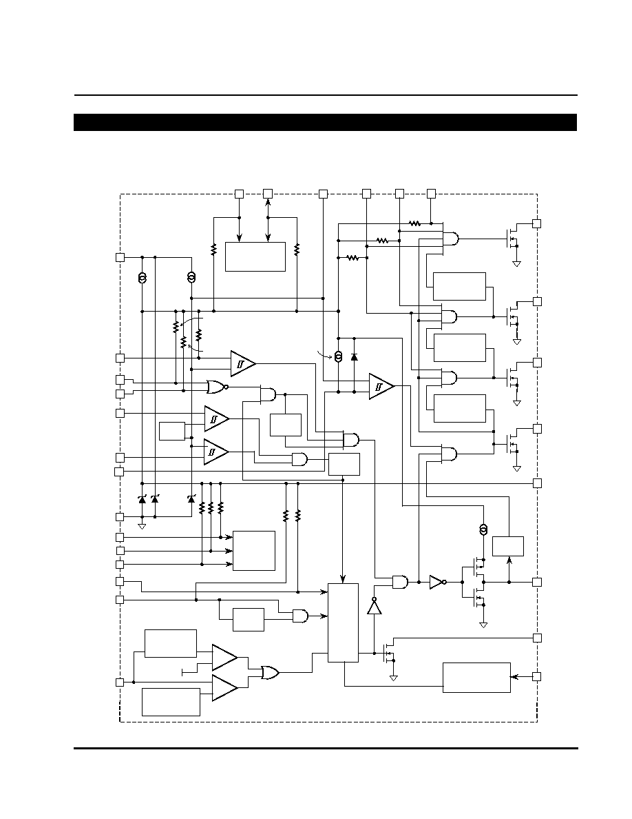
Functional Block Diagram
SMH4804
2
2050 3.7 10/30/02
Summit Microelectronics
≠
FUNCTIONAL BLOCK DIAGRAM
Figure 2. SMH4804 Block Diagram
PROGRAMM-
ABLE
DELAY
PROGRAMM-
ABLE
DELAY
PROGRAMM-
ABLE
DELAY
PROGRAMM-
ABLE
DELAY
+
≠
+
≠
+
≠
Programmable
Quick Response
Ref. Voltage
50mV
FAULT
LATCH
AND
DUTY
CYCLE
TIMER
P. D.
FILTER
+
≠
+
≠
5V
2.5V
12V
VGATE
SENSE
+
≠
VDD
VSS
MODE
RESET#
CBSENSE
EN/TS
PD1#
PD2#
UV
OV
PG3#
ENPGA ENPGB
2.5VREF
PG2#
PG1#
DRAIN
SENSE
VGATE
FAULT#
5.0VREF
12VREF
50k
200k
50k
PROG
REF
SDA
SCL
PROGRAMMING
STEERING
LOGIC
ENPGC
DEVICE
ADDRESS
DECODE
A2
A1
A0
PG4#
10µA
2050 BD
50k
50k
50k
50k
50k
Programmable
Shutdown
Timer
FS#
Three
@ 50k
50k
50k
OV/UV
FILTER
P. D.
FILTER
27
24
26
25
19
18
7
3
28
4
5
6
1
15
17
14
13
16
8
9
2
12
10
11
20
23
22
21

SMH4804
Functional Description
Summit Microelectronics
2050 3.7 10/30/02
3
≠\
FUNCTIONAL DESCRIPTION
The SMH4804 integrated hot swap power controller
operates within a wide supply range, typically -32 to -72
volts, and generates the signals necessary to drive isolated-
output DC/DC converters. The general start-up procedure is
as follows:
∑ A physical connection must first be made with the
chassis to discharge any electrostatic voltage potentials
when a typical add-in board is inserted into the powered
backplane.
∑ The board then contacts the long pins on the backplane
that provide power and ground.
∑ As soon as power is applied the device starts up, but
does not immediately apply power to the output load.
∑ Under-voltage and over-voltage circuits inside the
controller verify that the input voltage is within a user-
specified range.
∑ The SMH4804 senses the PD1# and PD2# pin
detection signals to indicate the card is seated properly.
These requirements must be met for a Pin Detect Delay
period of t
PDD
. Once this time has elapsed, the hot-swap
controller enables VGATE to turn on the external power
MOSFET switch. The VGATE output is current limited to
I
VGATE
, allowing the slew rate to be easily modified using
external passive components. During the controlled turn-on
period the V
DS
of the MOSFET is monitored by the drain
sense input. When DRAIN SENSE drops below 2.5V, and
VGATE rises above V
DD
≠ V
GT
, the SMH4804 asserts the
PG1# through PG4# power good outputs to enable the DC/
DC controllers. The ENPGA, ENPGB, and ENPGC Power
Good Enable inputs may be used to activate or deactivate
specific output loads.
Steady-state operation is maintained as long as all
conditions are normal. Any of the following events may
cause the device to disable the DC/DC controllers by
shutting down the power MOSFET:
∑ an under-voltage or over-voltage condition on the host
power supply.
∑ an over-current event detected on the CBSENSE input
∑ a failure of the power MOSFET sensed via the DRAIN
SENSE pin.
∑ the PD1#/PD2# pin detect signals becoming invalid.
∑ the master enable (EN/TS) falls below 2.5V.
∑ the FS# input is driven low by events on the secondary
side of the DC/DC controllers.
The SMH4804 may be configured so that after any of these
events occurs, the VGATE output shuts off and either
latches into an off state, or recycles power after a cooling
down period, t
CYC
.
Powering V
DD
The SMH4804 contains an internal shunt regulator on the
V
DD
pin that prevents the voltage from exceeding 12V. It is
necessary to use a dropper resistor (R
D
) between the host
power supply and the V
DD
pin in order to limit current into the
device and prevent possible damage. The dropper resistor
allows the device to operate across a wide range of system
supply voltages, typically -32 V to -72V, and also helps
protect the device against common-mode power surges.
Refer to the Applications Section for help on calculating the
R
D
resistance value.
Hot-Swap Verification
There are several enabling inputs that allow the host to
control the SMH4804. The Pin Detect signals (PD1# and
PD2#) are two active low enables that are generally used to
indicate that the add-in circuit card is properly seated.
These inputs must be held low for a pin-detect delay period
of t
PDD
before a power-up sequence may be initiated. This is
typically done by clamping the inputs to V
SS
through the
implementation of an ejector switch, or alternatively through
the use of staggered pins at the card-cage interface. The pin
detect delay (t
PDD
) timing parameter is controlled by bits 1:0
of register 9. Refer to Register 9 - Address 1001 on page 38
for more information.
Two shorter pins, arranged at opposite ends of the
connector, force the card to be fully seated before both pin
detects are enabled. Care must be taken not to exceed the
maximum voltage rating of these pins during the insertion
process. Refer to details in the Applications Section for
proper circuit implementation. Note that the PD1# and PD2#
inputs are enabled or disabled using bit 0 of Register 3.
Refer to Register 3 - Address 0011 on page 32 for more
information.
The EN/TS input provides an active high comparator input
that may be used as a master enable or temperature sense
input. This input signal must exceed 2.5V (nominal) for
proper operation. Refer to the Pin Descriptions on page 10
for more information.
Under-/Over-Voltage Sensing
The Under-Voltage (UV) and Over-Voltage (OV) inputs
provide a set of comparators that act in conjunction with an
external resistive divider ladder to sense whether or not the
host supply voltage is within the user-defined limits. The
power-up sequence is initiated when the input to the UV pin
rises above 2.5V and the input to the OV pin falls below
Functional Description
SMH4804
4
2050 3.7 10/30/02
Summit Microelectronics
2.5V for a period of at least t
PDD
(Pin Detect Delay time)
.
The t
PDD
filter helps prevent spurious start-up sequences
while the card is being inserted. If UV falls below 2.5V or OV
rises above 2.5V, the PG[4:1]# and VGATE outputs are
disabled immediately.
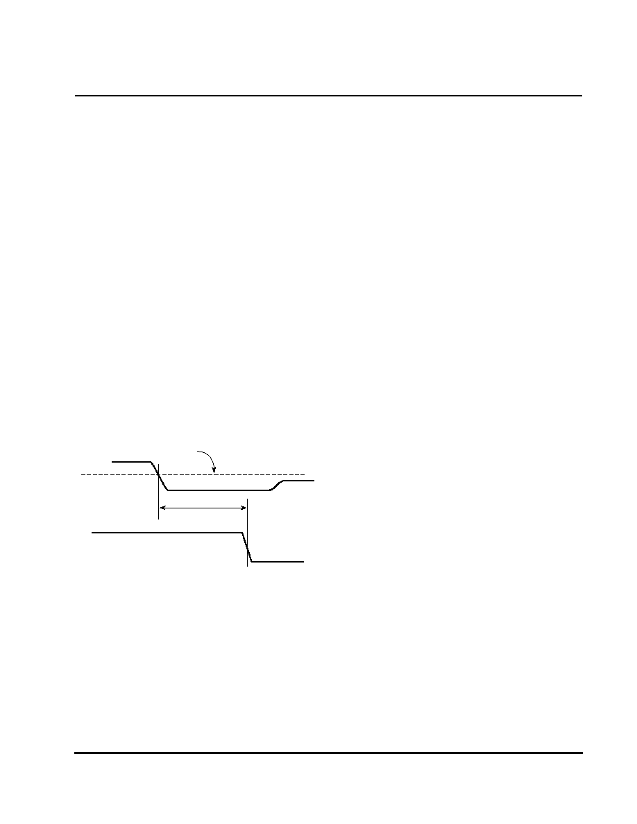
Under-/Over-Voltage Filtering
The SMH4804 can be configured so that an out-of-
tolerance condition on UV/OV does not shut off the output
immediately. Instead, a filter delay may be inserted so that
only sustained under-voltage or over-voltage conditions can
shut off the output. An out-of-tolerance condition on UV/OV
for longer than the filter delay time (t
UOFLTR
in Figure 3)
causes the VGATE and PG[4:1]# outputs to shut off when
the UV/OV filter option is enabled using bits 2:1 of Register
4. The under-/over-voltage filtering feature is disabled (bits
2:1 = 00) in the default configuration. Refer to Register 4 -
Address 0100 on page 33 for more information on the filter
delay options. The UV and OV filters are enabled and
disabled by programming bits 3 and 2 of Register 6
respectively. Refer to Register 6 - Address 0110 on page 36
for more information. Note that the delay values in Register
4 are only valid if the corresponding over or under voltage
filtering is enabled using bits 3:2 of Register 6.
Figure 3 shows the timing for the under-/over-voltage filter.
Figure 3. Under-/Over-Voltage Filter Timing
Under-/Over-Voltage Latching
An additional option for an out-of-tolerance condition on UV/
OV is to latch the VGATE and PG[4:1]# outputs off such that
a return to normal UV/OV operation does not turn them back
on. In this case the FAULT# output is asserted.
Under-Voltage Hysteresis
The Under-Voltage comparator input may be configured
with a programmable level of hysteresis using Register 7.
The falling voltage compare level may be set in steps of
62.5mV below 2.5V. The rising voltage compare level is
fixed at 2.5V. The default under-voltage hysteresis level is
set to 62.5mV. In default conditions the SMH4804 is not in
an under-voltage state once the UV voltage rises above
2.5V; and after that an under-voltage occurrence is not
recognized until the UV voltage falls below 2.4375V (2.5V ≠
62.5mV).
Soft Start Slew Rate Control
Once all of the preconditions for powering up the DC/DC
controllers have been met as explained in the previous
sections, the SMH4804 provides a means to soft start the
external power MOSFET. It is important to limit in-rush
current to prevent damage to the add-in card or disruptions
to the host power supply. For example, charging the filter
capacitance too quickly (normally required at the input of the
DC/DC controllers) may generate very high current. The
VGATE output of the SMH4804 is current limited to I
VGATE
,
allowing the slew rate to be easily modified using external
passive components. The slew rate may be found by
dividing I
VGATE
by the gate-to-drain capacitance placed on
the external FET.
Load Control -- Sequencing the Secondary
Supplies
The PG1# through PG4# output pins are used to enable the
external DC/DC controllers. Once the card is inserted, the
SMH4804 samples the PD1# and PD2# pin detect input
pins to determine if the card as been inserted properly. It
then monitors the state of the UV and OV input pins to
assure there is no under-voltage or over-voltage condition
present. Once these conditions are met, and the EN/TS pin
is greater than 2.5V, the SMH4804 asserts the VGATE
output to turn on the external MOSFET.
During the time it takes to turn the MOSFET on, the
SMH4804 monitors the system for an over-current condition
via the CBSENSE input pin. In addition, the device internally
monitors the voltage level on the VGATE output pin. This is
shown by the `VGATE Sense' block in Figure 2.
Once power has been ramped to the DC/DC controllers, two
conditions must be met before the PG[4:1]# outputs can be
enabled:
∑ the DRAIN SENSE input voltage must be below 2.5V.
∑ the VGATE voltage must be greater than V
DD
≠ V
GT
,
where V
GT
is the gate threshold.
The DRAIN SENSE input helps ensure that the power
MOSFET is not absorbing too much steady state power
from operating at a high V
DS
. This sensor remains active at
all times (except when current regulation is enabled). The
2050 Fig07
OV / UV
FAULT#
t
UOFLTR
2.5V
SMH4804
Functional Description
Summit Microelectronics
2050 3.7 10/30/02
5
VGATE sensor makes sure that the power MOSFET is
operating well into its saturation region before allowing the
loads to be switched on. Once VGATE reaches V
DD
≠ V
GT
this sensor is latched.
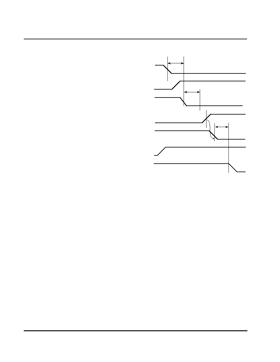
When the external MOSFET is properly switched on the
PG[4:1]# outputs may be enabled. Output PG1# is activated
first, followed by PG2# after a delay of t
PGD,
PG3# after
another t
PGD
delay, and PG4# after a final t
PGD
delay. The
delays built into the SMH4804 allow timed sequencing of
power to the loads. The delay times are programmable from
50µs to 160ms using bits 3:2 of Register 3 and bit 3 of
Register 9. Refer to Register 3 - Address 0011 on page 32
and Register 9 - Address 1001 on page 38 for more
information.
The ENPGA, ENPGB, and ENPGC input pins in Figure 5
are used to enabled the PG[4:1]# outputs. The ENPGA pin
controls the PG[4:2]# outputs. If ENPGA is deasserted by
external logic, the SMH4804 disables the PG[4:2]# outputs
and they enter the high-impedance state. The ENPGA input
must be asserted in order for PG[4:2]# to be driven by the
SMH4804.
The ENPGB pin controls the PG[4:3]# outputs. If ENPGB is
deasserted by external logic, the SMH4804 disables the
PG[4:3]# outputs and they enter the high-impedance state.
The ENPGB input must be asserted in order for PG[4:3]# to
be driven by the SMH4804.
The ENPGC pin controls the PG[4]# output. If ENPGC is
deasserted by external logic, the SMH4804 disables the
PG[4]# outputs and the output enters the high-impedance
state. The ENPGC input must be asserted in order for
PG[4]# to be driven by the SMH4804.
This cascaded control mechanism is useful for enabling
supplies that have dependencies based on the other
voltages in the system.
The PG[4:1] outputs have a 12V withstand capability, so
high voltages must not be connected to these pins. Bipolar
transistors or opto-isolators can be used to boost the
withstand voltage to that of the host supply. Refer to
Figure 18 for connectivity information.
Figure 5 shows the relationship between the PG[4:1]# and
the ENPG[C:A] signals.
Figure 4. PG Output and ENPG Input Relationship
Forced Shutdown -- Secondary Feedback
The Forced Shutdown signal (FS#) is an active low input
that provides a method of receiving feedback from the
secondary side of the DC/DC controllers. A built-in
shutdown timer allows the SMH4804 to ignore the state of
the FS# input until the timer period expires. The timer period
is defined in bits 2:0 of Register 5. The FS# input must be
driven high by the end of this timer period. A low level on this
input causes a Fault condition, driving the FAULT# pin low
and shutting off the VGATE and PG[4:1]# outputs.
The purpose of the shutdown timer is to allow enough time
for devices on the secondary side of the DC/DC controllers
to power up and stabilize. This feature allows supervisory
circuits such as an SMS44 to control the shutdown of the
primary side soft start circuit, even though the secondary
side initially has no power.
Alternatively, the FS# input can be programmed to act as a
fourth ENPG input controlling the PG1# output. This is
combined with an option to independently enable PG1#
with no affect on the other PG[4:2]# outputs, or it can be
programmed so PG1# is the enabling output for the other
outputs.
2050 Fig02 2.1
PG1#
PG2#
PG3#
PG4#
ENPGA
ENPGC
ENPGB
t
PGD
t
PGD
t
PGD