 | –≠–ª–µ–∫—Ç—Ä–æ–Ω–Ω—ã–π –∫–æ–º–ø–æ–Ω–µ–Ω—Ç: SMH4812S | –°–∫–∞—á–∞—Ç—å:  PDF PDF  ZIP ZIP |

1
Characteristics subject to change without notice
2055 4.0 12/22/00
SMH4812
SUMMIT
MICROELECTRONICS, Inc.
©SUMMIT MICROELECTRONICS, Inc., 2000 ∑ 300 Orchard City Dr., Suite 131 ∑ Campbell, CA 95008 ∑ Phone 408-378-3970 ∑ FAX 408-378-6586 ∑ www.summitmicro.com
Preliminary
Distributed Power Hot-Swap Controller
FEATURES
SIMPLIFIED APPLICATION DRAWING
!
!
!
!
!
Soft Starts Main Power Supply on Card Insertion
or System Power Up
!
!
!
!
!
Senses Card Insertion via Short Pins or Ejector
Switches
!
!
!
!
!
Master Enable to Allow System Control of Power
Up or Down
"
""
"
"
Can be used as a Temperature Sense Input
!
!
!
!
!
Programmable Independent Controls of a DC/DC
Converter
"
""
"
"
Not Enabled until Host Supply Fully Soft
Started
"
""
"
"
Programmable Time Delay
"
""
"
"
Available Input to hold off Dependant Enables
until Conditions are Satisfied
!
!
!
!
!
Highly Programmable Circuit Breaker
"
""
"
"
Programmable Quick-Trip
TM
Values
"
""
"
"
Programmable Current Limiting
"
""
"
"
Programmable Duty Cycle Times
"
""
"
"
Programmable Over-current Filter
!
!
!
!
!
Programmable Host Voltage Fault Monitoring
"
""
"
"
Programmable Under-Voltage Hysteresis
"
""
"
"
Programmable UV/OV Voltage Filter
"
""
"
"
Programmable Fault Mode: Latched or Duty
Cycle
!
!
!
!
!
Programmable Forced Shutdown Timer
!
!
!
!
!
2.5V and 5.0V Reference Outputs
"
""
"
"
Eliminates the Need for Other Primary Volt-
ages
"
""
"
"
Easy Expansion of External Monitor Func-
tions
!
!
!
!
!
Supply Range +20VDC to >+500VDC
VDD
VSS
CBSENSE
PD1#
PD2#
UV
OV
2.5VREF
PG2#
5.0VREF
2055 SAD 1.1
0V
≠48V
VGATE
Pin Detect
Pin Detect
DC/DC
SMH4812
FAULT#
ENPG
Disable/Enable
FS#
2
SMH4812
2055 4.0 12/22/00
SUMMIT MICROELECTRONICS, Inc.
Preliminary
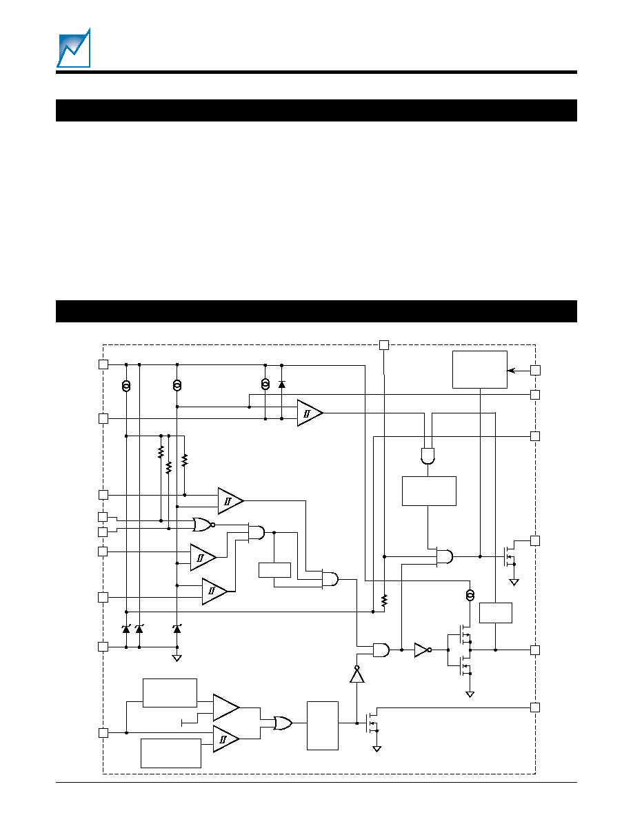
FUNCTIONAL BLOCK DIAGRAM
PROGRAMM-
ABLE
DELAY
PROGRAMM-
ABLE
DELAY
+
≠
+
≠
+
≠
Programmable
Quick Response
Ref. Voltage
50mV
DUTY
CYCLE
TIMER
FILTER
+
≠
+
≠
5V
2.5V
12V
VGATE
SENSE
+
≠
VDD
VSS
CBSENSE
EN/TS
PD1#
PD2#
UV
OV
ENPG
2.5VREF
PG#
DRAIN
SENSE
VGATE
FAULT#
5.0VREF
12VREF
2055 BD 3.0
PROGRAMM-
ABLE
SHUTDOWN
TIMER
FS#
16
3
1
4
10
8
5
9
7
2
6
11
15
13
12
14
50k
50k
50k
50k
The SMH4812 is designed to control hot swapping of plug-
in cards operating from a single supply, which can have an
output range from 20V to 500V. The SMH4812 hot-swap
controller provides under-voltage and over-voltage moni-
toring of the host power supply, it drives an external power
MOSFET switch that connects the supply to the load, and
it protects against over-current conditions that might dis-
rupt the host supply. When the input and output voltages
to the SMH4812 controller are within specification it pro-
DESCRIPTION
vides a Power Good logic output that may be used to
enable a DC-DC converter. Additional features of the
device include: temperature sense or master enable
input, 2.5V and 5V reference outputs for expanding moni-
tor functions, two Pin-Detect enable inputs for fault protec-
tion, and duty-cycle or latched over-current protection
modes. All of these features can be programmed by the
factory according to the user's requirements.

3
2055 4.0 12/22/00
SMH4812
SUMMIT MICROELECTRONICS, Inc.
Preliminary
PIN CONFIGURATION
PIN DESCRIPTIONS
DRAIN SENSE (1)
The DRAIN SENSE input monitors the voltage at the drain
of the external power MOSFET switch with respect to V
SS
.
An internal 10µA source pulls the DRAIN SENSE signal
towards the 5V reference level. DRAIN SENSE must be
held below 2.5V to enable the PG outputs.
EN/TS (3)
The Enable/Temperature Sense input is the master en-
able input. If EN/TS is less than 2.5V, VGATE will be
disabled. This pin has an internal 200kW pull-up to 5V.
PD1#, PD2# (4, 5)
These are logic level active low inputs that can optionally
be employed to enable VGATE and the PG outputs when
they are at V
SS
. These pins each have an internal 50kW
pull-up to 5V.
CBSENSE (7)
The circuit breaker sense input is used to detect over-
current conditions across an external, low value sense
resistor (R
S
) tied in series with the Power MOSFET. A
voltage drop of greater than 50mV across the resistor for
longer than t
CBD
will trip the circuit breaker. A program-
mable Quick-Trip sense point is also available.
UV (9)
The UV pin is used as an under-voltage supply monitor,
typically in conjunction with an external resistor ladder.
VGATE will be disabled if UV is less than 2.5V. Program-
mable internal hysteresis is available on the UV input,
adjustable in increments of 62.5mV. Also available is a
filter delay on the UV input.
OV (10)
The OV pin is used as an over-voltage supply monitor,
typically in conjunction with an external resistor ladder.
VGATE will be disabled if OV is greater than 2.5V. A filter
delay is available on the OV input.
VGATE (2)
The VGATE output activates an external power MOSFET
switch. This signal supplies a constant current output
(100µA typical), which allows easy adjustment of the
MOSFET turn on slew rate.
FAULT# (6)
FAULT# is an open-drain, active-low output that indicates
the fault status of the device.
5VREF (11)
This is a precision 5V output reference voltage that may be
used to expand the logic input functions on the SMH4812.
The reference output is with respect to V
SS
.
2.5VREF (12)
This is a precision 2.5V output reference voltage that may
be used to expand the logic input functions on the
SMH4812. The reference output is with respect to V
SS
.
FS# (13)
The Forced Shutdown (FS#) pin is an active low input that
causes VGATE and PG outputs to be shut down at any
time after an internal hold-off timer has expired. The hold-
off timer allows supervisory circuits on the secondary side
(which are not powered up initially) to control shut down of
the SMH4812 via an opto-isolator. This input has no pull-
up resistor.
DRAIN SENSE
VGATE
EN/TS
PD1#
PD2#
FAULT#
CBSENSE
V
SS
V
DD
PG#
ENPG
FS#
2.5V
REF
5V
REF
OV
UV
1
2
3
4
5
6
7
8
16
15
14
13
12
11
10
9
2055 PCon 2.0

4
SMH4812
2055 4.0 12/22/00
SUMMIT MICROELECTRONICS, Inc.
Preliminary
ENPG (14)
The ENPG input controls the PG# output. When ENPG is
pulled low the PG# output is immediately placed in a high
impedance state. If ENPG is driven high then the PG#
output will immediately be driven low.
PG# (15)
PG# is an open-drain, active-low output with no internal
pull-up resistor. It can be used to switch a load or enable
a DC/DC converter. PG# is enabled immediately after
VGATE reaches V
DD
≠ V
GT
and the DRAIN SENSE
voltage is less than 2.5V. Voltage on these pins cannot
exceed 12V, as referenced to V
SS.
V
DD
(16)
V
DD
is the positive supply connection. An internal shunt
regulator connected between V
DD
and V
SS
develops ap-
proximately 12V that supplies the SMH4812. A resistor
must be placed in series with the V
DD
pin to limit the
regulator current (RD in the application illustrations).
V
SS
(8)
V
SS
is connected to the negative side of the supply.
5
2055 4.0 12/22/00
SMH4812
SUMMIT MICROELECTRONICS, Inc.
Preliminary
2055 Prog Table
*COMMENT
Stresses listed under Absolute Maximum Ratings may cause perma-
nent damage to the device. These are stress ratings only, and
functional operation of the device at these or any other conditions
outside those listed in the operational sections of this specification is not
implied. Exposure to any absolute maximum rating for extended
periods may affect device performance and reliability.
Temperature Under Bias ...................... ≠55∞C to 125∞C
Storage Temperature ........................... ≠65∞C to 150∞C
Lead Solder Temperature (10 secs) ................... 300 ∞C
Terminal Voltage with Respect to V
SS
:
V
DD
................................. ≠0.5V to V
DD
OV, UV, DRAIN SENSE,
FS#, CBSENSE ..... ≠0.5V to V
DD
+0.5V
PD1#, PD2#, ENPG, EN/TS ......... 10V
FAULT#, PG# ........ ≠0.5V to V
DD
+0.5V
VGATE ................................ V
DD
+0.5V
ABSOLUTE MAXIMUM RATINGS*
AC OPERATING CHARACTERISTICS
l
o
b
m
y
S
n
o
i
t
p
i
r
c
s
e
D
.
n
i
M
.
p
y
T
.
x
a
M
s
t
i
n
U
t
D
B
C
y
a
l
e
d
r
e
k
a
e
r
B
t
i
u
c
r
i
C
V
m
0
5
e
l
b
a
m
m
a
r
g
o
r
P
)
r
e
t
li
f
(
5
s
µ
0
5
*
s
µ
0
5
1
s
µ
0
0
4
s
µ
t
D
G
V
y
a
l
e
d
d
o
o
G
r
e
w
o
P
e
l
b
a
m
m
a
r
g
o
r
P
0
5
s
µ
0
5
2
s
µ
0
0
5
s
µ
0
0
5
1
s
µ
5
*
s
m
0
2
s
m
0
8
s
m
0
6
1
s
m
t
N
D
T
H
S
T
S
F
V
o
t
t
l
u
a
F
m
o
r
f
y
a
l
e
d
n
w
o
d
t
u
h
s
t
s
a
F
E
T
A
G
f
f
o
0
0
2
s
n
t
C
Y
C
e
m
i
t
e
l
c
y
c
r
e
k
a
e
r
b
t
i
u
c
r
i
C
5
.
2
s
t
T
S
R
B
C
B
C
T
E
S
E
R
h
t
d
i
w
e
s
l
u
p
0
0
2
s
n
t
F
V
U
P
r
e
t
li
f
e
g
a
t
l
o
V
-
r
e
d
n
U
e
l
b
a
m
m
a
r
g
o
r
P
F
F
O
*
--
5
s
m
0
8
s
m
0
6
1
s
m
t
D
D
P
t
c
e
t
e
D
n
i
P
e
l
b
a
m
m
a
r
g
o
r
P
5
.
0
s
m
5
s
m
0
8
*
s
m
0
6
1
s
m
*
= Default value