SMH4814
Preliminary Information
1
(See Last Page)
© SUMMIT Microelectronics, Inc.
2005 ∑ 1717 Fox Drive ∑ San Jose CA 95131 ∑ Phone 408 436-9890 ∑ FAX 408 436-9897
The Summit Web Site can be accessed by "right" or "left" mouse clicking on the link:
http://www.summitmicro.com/
2080 2.0 07/21/05
1
Dual Feed Active-ORing Programmable Hot Swap Controller
FEATURES AND APPLICATIONS
Eliminates Passive ORing Diodes for Reduced
Power Consumption
High Noise Immunity on All Logic Inputs
Soft Starts Main Power Supply on Card
Insertion or System Power Up with Slew Rate
Control
Programmable Differential Current Sense
∑ Programmable Inrush Current Limiting
∑ Master Enable to Allow System Control of
Power-Up or -Down
Programmable Independent Enabling of up to
4 DC/DC Converters
Programmable Circuit Breaker Level and Mode
Programmable Quick-TripTM Value, Current
Limiting, Duty Cycle Times, Over-Current Filter
Programmable Host Voltage Fault Monitoring
Programmable UV/OV Filter and Hysteresis
Programmable Fault Mode: Latched or Duty
Cycle
Internal Shunt Regulator Allows for a Wide
Supply Range
Applications
Telecom Hot-Swap Card - AdvancedTCA
TM
Network
Processors
Power-on Ethernet, IEEE 802.3af
INTRODUCTION
The SMH4814 is an integrated power controller
designed to control the hot-swapping of plug-in cards
in a distributed power environment. The SMH4814
drives external power MOSFET switches that connect
the supply to the load while reducing in-rush current
and providing over-current protection. When the
source and drain voltages of the external MOSFETs
are within specification the SMH4814 asserts the four
PUP logic outputs in a programmable cascade
sequence to enable the DC/DC converters.
The SMH4814 also monitors two independent ≠48V
feeds. The redundant power supplies allow for high
availability and reliability. The traditional method of
supplying power from these feeds is via ORing power
diodes, which consume a significant amount of power.
The SMH4814 allows low-RDS
ON
FETs to be used in
place of ORing diodes to reduce power consumption.
The SMH4814 determines when at least one of the
≠48V feeds is within an acceptable voltage range and
switches on the appropriate FET path while providing
slew rate control. The SMH4814 continuously monitors
the incoming feeds and switches to the most negative
feed as necessary. The SMH4814 is programmed and
controlled using the I
2
C bus as required in ATCA
TM
applications.
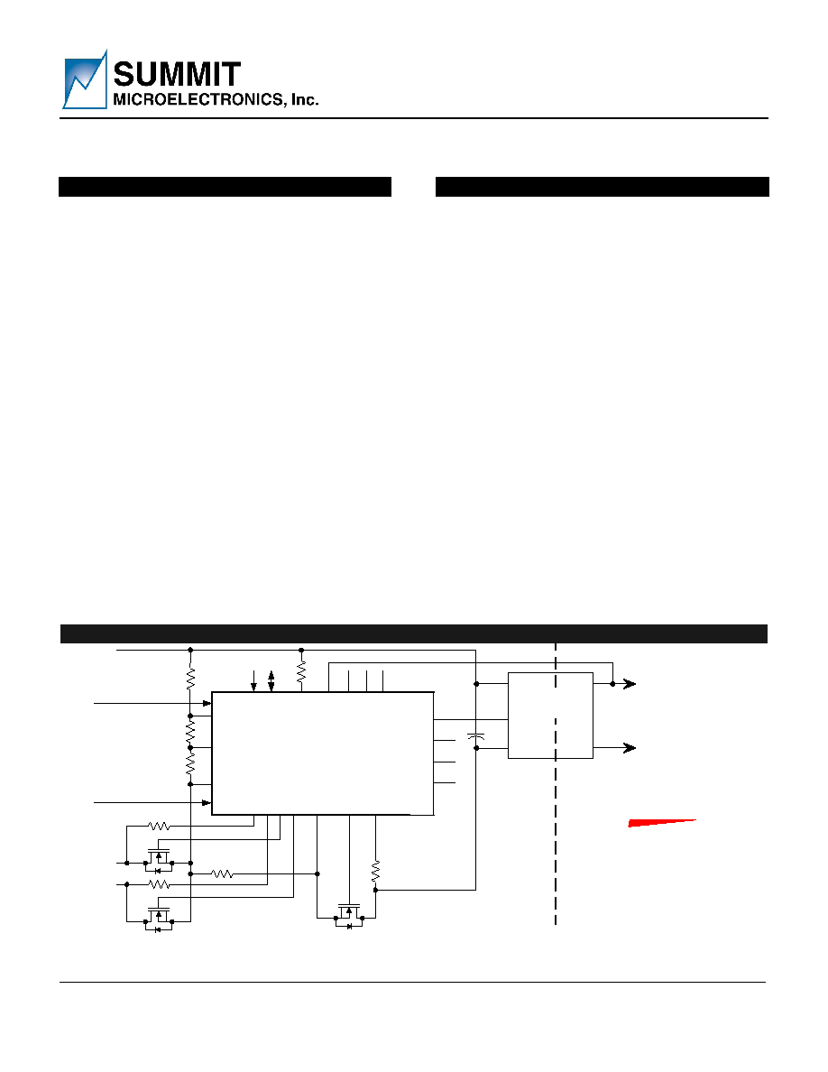
≠48V Ret.
R
D
UV
OV
VSS
V1
2
SMH4814
F
EED
A
F
EED
B
VGA
TE
A
VGA
TE
B
C
B
SEN
SE
≠48V A
≠48V B
PUP
A
PUP
B
PUP
C
PUP
D
VGA
TE
_HS
DRAI
N
SE
NS
E
V
IN
+
V
OUT
+
V
OUT
-
V
IN
-
ON/OFF
FB
A
FB
B
FB
C
FB
D
Primary
Secondary
R
S
PD0
PD1
Pin
Detect
Pin
Detect
SC
L
SD
A
I
2
C
DC-to-DC
Converter A
R
A
R
B
Figure 1. The SMH4814 Controller hot-swaps and cascade sequences up to 4 DC/DC Converters and actively
controls the A and B ≠48V feeds eliminating the need for ORing diodes and the associated voltage drop.
Note: This is an applications example only. Some pins, components and values are not shown.
SIMPLIFIED APPLICATIONS DRAWING
A
dvanced
T
CA
TM

SMH4814
Preliminary Information
Summit Microelectronics, Inc
2080 2.0 07/21/05
2
GENERAL DESCRIPTION
The SMH4814 integrated power controller operates
within a wide supply range, typically ≠32 to ≠72 volts,
and generates the signals necessary to drive isolated-
output DC/DC converters.
The device accepts two independent ≠48V feeds via
input pins FEED
A
and FEED
B
. The VGATE
A
pin
controls the flow of power from FEED
A
to the load.
The VGATE
B
pin controls the flow of power from
FEED
B
to the load.
The SMH4814 continuously monitors the voltage on
FEED
A
and FEED
B
. The supply arbitration block in
Figure 2 selects which pin drives power to the device
based on the voltage level on each pin and the
acceptable voltage range. Once the FEED
A
or FEED
B
pin is selected the SMH4814 asserts the
corresponding VGATE pin. The assertion of this pin
turns on the external low-RDS
ON
FETs to supply power
to the load.
Start-up Procedure
The general start-up procedure is as follows:
1. A physical connection must be made with the
chassis to discharge any electrostatic voltage
potentials when a typical add-in board is inserted
into the powered backplane.
2. The board then contacts the long pins on the
backplane that provide power and ground.
3. As soon as power is applied the device starts up,
but it does not immediately apply power to the
output load.
4. Under-voltage and over-voltage circuits inside the
controller verify that the input voltage is within a
user-specified range.
5. The SMH4814 senses the PD1 and PD0 pin
detection signals to indicate the card is seated
properly.
These requirements must be met for a Pin Detect
Delay period of t
PDD
. Once this time has elapsed the
hot-swap controller enables VGATE_HS to turn on the
external power MOSFET switch.
The VGATE_HS output is current limited to I
VGATE
,
allowing the slew rate to be easily modified using
external passive components. During the controlled
turn-on period the V
DS
of the MOSFET is monitored by
the DRAIN SENSE input. When DRAIN SENSE drops
below 2.5V, and VGATE_HS rises above V12 ≠ V
GT
,
the SMH4814 asserts the PUP
A
through PUP
D
power
good outputs to enable the DC/DC controllers.
Steady-state operation is maintained as long as all
conditions are normal. Any of the following events
may cause the device to disable the DC/DC controllers
by shutting down the power MOSFETs:
An under-voltage or over-voltage condition on the
host power supply.
A failure of the power MOSFET sensed via the
DRAIN SENSE pin.
The PD1/PD0 pin detect signals becoming invalid.
The master enable (EN/TS) falls below 2.5V.
Any of the FB inputs driven low by events on the
secondary side of the DC/DC controllers.
The occurrence of an overcurrent.
The SMH4814 may be configured so that after any of
these events occurs the VGATE output shuts off, and
either latches into an off state or recycles power after
a cooling down period, t
CYC
.
Powering V12
The SMH4814 contains an internal shunt regulator on
the V12 pin that prevents the voltage from exceeding
12V. It is necessary to use a dropping resistor (R
D
)
between the host power supply and the V12 pin in
order to limit current into the device and prevent
possible damage. The dropping resistor allows the
device to operate across a wide range of system
supply voltages, typically ≠32 V to ≠72V, and also
helps protect the device against common-mode power
surges. Refer to the Applications Section for help on
calculating the R
D
resistance value.
SMH4814
Preliminary Information
Summit Microelectronics, Inc
2080 2.0 07/21/05
3
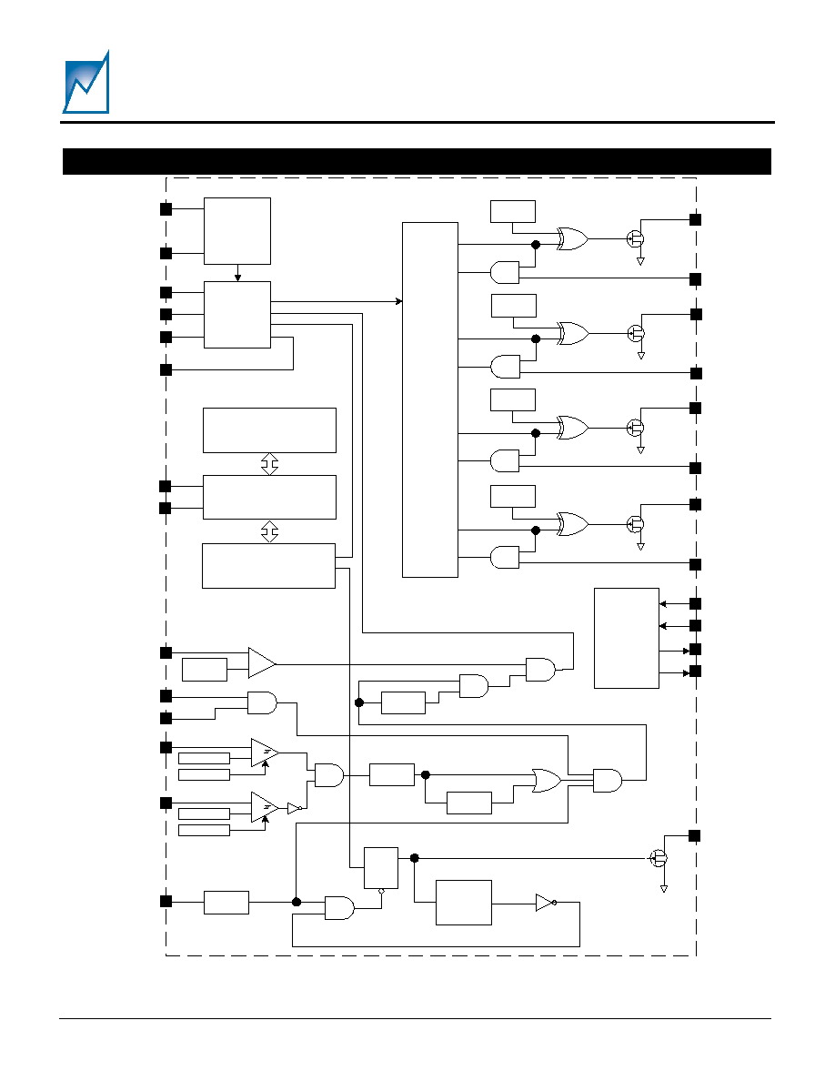
Voltage
Regulator
and
Reference
Generator
V12
5V_CAP
CB Sense
and Gate
Control
CBSENSE
SLEW
DRAIN_SENSE
VGATE_HS
E
2
Memory
Configuration, Status,
and Command Registers
I2C Interface
Virtual Address A2, A1
SCL
SDA
ENTS
+
-
2.5V Ref
PD0
PD1
+
-
Prog Ref
UV
Prog Hyst
+
-
Prog Ref
OV
Prog Hyst
Glitch
Filter
UV/OV
Filter
PO
Filter
Glitch
Filter
RESET#
Fault
Latch
Duty Cycle
Timer
FAULT#
PUP
A
Polarity
PUP
A
FB
A
PUP
B
Polarity
PUP
B
FB
B
PUP
C
Polarity
PUP
C
FB
C
PUP
D
Polarity
PUP
D
FB
D
Time
Slot and
PUP
Control
FEED
A
FEED
B
GATE
A
GATE
B
Supply
Arbitration
Programmable Fault
Conditions
Figure 2. Block Diagram
INTERNAL FUNCTIONAL BLOCK DIAGRAM

SMH4814
Preliminary Information
Summit Microelectronics, Inc
2080 2.0 07/21/05
4
PIN DESCRIPTION
Pin No.
QFN
Pin Type
Name
Description
1,2 I PD0,
PD1
The PD pins are active high, logic level inputs. Protection diodes allow
them to be overdriven when used in conjunction with a series limiting
resistor. The PD pins have an internal pull-down current sink of 10uA
typical.
3 I RESET#
The RESET# pin is used to clear latched fault conditions. When this pin is
asserted, the VGATE
X
and PUP
X
outputs are immediately disabled. Refer to
the section on Circuit Breaker Operation for more information. The RESET#
pin has an internal pull-up current source to 5V_CAP of 10uA typical.
4 I SCL
SCL is the serial clock input.
5 I/O SDA
SDA is the bidirectional serial data I/O port.
6,
7,
8,
9
O
PUP
A
, PUP
B
,
PUP
C
,
PUP
D
The PUP
X
outputs are programmable active high/low open drain converter
enable pins. They can be used in one of 4 programmable sequence
positions to switch a load or enable a DC/DC converter after a
programmable delay, t
PGDn
. The voltage on these pins cannot exceed 12V
relative to V
SS
.
10 O FAULT#
FAULT# is an open-drain, active-low output that indicates the fault status of
the device. The device's Status Register may be polled to determine more
detailed information about the fault condition.
11 PWR VSS This is connected to the negative side of the supply.
12 I
CBSENSE
The circuit breaker sense input is used to detect over-current conditions
across an external, low value sense resistor (R
S
)
tied in series with the
Power MOSFET. A voltage drop of greater than V
CB
(programmable level)
across the resistor for longer than t
CBD
trips the circuit breaker. A
programmable Quick-TripTM sense point is also available.
13 I UV
The UV pin is used as an under-voltage supply monitor, typically in
conjunction with an external resistor ladder. VGATE_HS is enabled when
the UV input > Vuv and disabled when UV < Vuv-Vuvhys. An optional
programmable filter delay is also available on the UV input.
14 I OV
The OV pin is used as an over-voltage supply monitor, typically in
conjunction with an external resistor ladder. VGATE_HS is disabled when
OV > Vov and enabled when OV < Vov-Vovhys. A filter delay is also
available on the OV input.
15 I EN/TS
The Enable/Temperature Sense input is the master enable input. If EN/TS
is less than 2.5V, all VGATE outputs are disabled.
16 I
SLEW_CNTL
A capacitor connected to this pin controls the VGATE_HS Slew Rate.
17 I FEED
B
Connect to the -48V 'B' feed using a series 100k resistor. The voltage on
this pin is compared with the voltage on the FEED
A
pin internally by the
supply arbitration logic to determine which voltage will be used.
SMH4814
Preliminary Information
Summit Microelectronics, Inc
2080 2.0 07/21/05
5
PIN DESCRIPTION (CONTINUED)
Pin No.
QFN
Pin Type
Name
Description
18 I FEED
A
Connect to the -48V 'A' feed using a series 100k resistor. The voltage on
this pin is compared with the voltage on the FEED
B
pin internally by the
supply arbitration logic to determine which voltage will be used.
19 I DRAIN
SENSE
The DRAIN SENSE input monitors the voltage at the drain of the external
power MOSFET switch with respect to VSS. An internal 10µA source pulls
the DRAIN SENSE signal towards the 5V_CAP level. DRAIN SENSE must
be held below 2.5V to enable the PUP
X
outputs.
20 O 5V_CAP
External capacitor input used to filter the device's internal operating supply.
Also a hold Capacitor to sequence down and to filter any power glitches.
21 O
VGATE_HS
The VGATE_HS output activates an external power MOSFET switch. This
signal controls inrush current by modulating the gate of the Hot Swap
MOSFET device. It supplies a programmable current output which allows
easy adjustment of the MOSFET turn-on slew rate.
22 O VGATE
B
This pin controls the gate of the active FET on FEED
B
.
23 O VGATE
A
This pin controls the gate of the active FET on FEED
A
24 PWR V12 This is the positive supply input. An internal shunt regulator limits the
voltage on this pin to approximately 12V with respect to V
SS
. A resistor
must be placed in series with the V12 pin to limit the regulator current (R
D
in
the application schematics).
25 I FB
D
Active-high, logic level input that can be used to indicate when the converter
controlled by PUP
D
is fully powered.
A hold-off timer allows the secondary
side (which is not powered up initially) to control shut down via an opto-
isolator. See Figures 5 and 6.
26 I FB
C
Active-high, logic level input that can be used to indicate when the converter
controlled by PUP
C
is fully powered.
A hold-off timer allows the secondary
side (which is not powered up initially) to control shut down via an opto-
isolator. See Figures 5 and 6.
27 I FB
B
Active-high, logic level input that can be used to indicate when the converter
controlled by PUP
B
is fully powered.
A hold-off timer allows the secondary
side (which is not powered up initially) to control shut down via an opto-
isolator. See Figures 5 and 6.
28 I FB
A
Active-high, logic level input that can be used to indicate when the converter
controlled by PUP
A
is fully powered.
A hold-off timer allows the secondary
side (which is not powered up initially) to control shut down via an opto-
isolator. See Figures 5 and 6.