SMM605
Preliminary Information
1
(See Last Page)
© SUMMIT Microelectronics, Inc. 2003
∑
1717 Fox Drive ∑ San Jose CA 95131 ∑ Phone 408 436-9890 ∑ FAX 408 436-9897
www.summitmicro.com
2064 1.1 9/16/03
1
FEATURES & APPLICATIONS
∑ Extremely accurate (±0.1% Typ.) Active
DC Output Control (ADOC
TM
)
∑ Six channel control of DC/DC converters
∑ ADOC Automatically adjusts supply output
voltage level under all DC load conditions
∑ Capable of margining supplies with trim inputs
using either positive or negative trim pin control
∑ Wide Margin/ADOC range from 0.35V to VDD
∑ Uses either an internal or external VREF
∑ Operates from any intermediate bus supply
from 8V to 15V and from 2.7V to 5.5V
∑ Programmable START and READY pins
∑ General Purpose 4k EEPROM with Write Protect
∑ I
2
C 2-wire serial bus for programming
configuration and monitoring status.
∑ 48 lead TQFP package
Applications
∑ Monitor/Control Distributed and POL Supplies
∑ Multi-voltage Processors, DSPs, ASICs used in
Telecom, CompactPCI or server systems
INTRODUCTION
The SMM605 actively controls the output voltage level
of up to six DC/DC converters that use a `Trim' or
`VADJ/FB' pin to adjust the output. An Active DC
Output Control (ADOC
TM
) feature is used during
normal operation to maintain extremely accurate
settings of supply voltages and, during system test, to
control margining of the supplies using the industry
standard I
2
C 2-wire data bus commands. Total
accuracy with a ±0.1% external reference is ±0.2%,
and ±0.5% using the internal reference. The device
can margin supplies with either positive or negative
trim pin control within a range of 0.35V to VDD. The
SMM605 supply can range from 2.7V to 5.5V or 6V to
14V to accommodate any intermediate bus supply.
The voltage settings (margin high/low and
nominal) are programmed into nonvolatile memory.
The I
2
C bus is used to enable margin high, margin low,
ADOC or normal operation. When margining, the
SMM605 will check the voltage output of the converter
and make adjustments to the trim pin via a feedback
loop to bring the voltage to the margin setting. A
margining status register is set to indicate that the
system is ready for test.
Six-Channel Supply Voltage Marginer and Active DC Output Controller (ADOC
TM
)
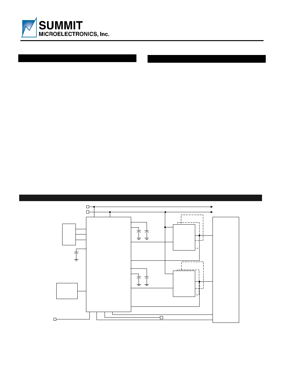
SIMPLIFIED APPLICATIONS DRAWING
TRIM
B
VM
B
TRIM_CAP
B
CAP
B
TRIM
A
VM
A
TRIM_CAP
A
CAP
A
SMM605
µP/
ASIC
VD
D
RS
T
RE
ADY
MR
3.3VIN (+2.7V to +5.5V Range)
RESET
READY
HEALTHY
12VIN
12VIN (+6V to +14V Range)
2.5VIN
1.2VIN
12V
SDA
SCL
I
2
C
BUS
3.3V
A2
VREF_CNTL
VIN
TRIM
Vout
DC/DC
Converter A
VIN
TRIM
Vout
DC/DC
Converter B
External or
Internal
REFERENCE
DC/DC
Converter C, E
DC/DC
Converter D, F
2 of 6 DC-DC
Converters shown
ST
A
R
T
POWER GOOD
VDD_CAP
Figure 1 ≠ Applications Schematic using the SMM605 Controller to actively control and margin the output
levels of up to six DC/DC Converters.
Note: This is an applications example only. Some pins, components and values are not shown.
SMM605
Preliminary Information
Summit Microelectronics, Inc
2064 1.1 09/16/03
2
GENERAL DESCRIPTION
The SMM605 is capable of controlling the DC output
of up to six DC/DC Modules, switching regulators or
LDOs that use a trim/adjust pin and automatically
change the level using a unique Active DC Output
Control (ADOC
TM
). The ADOC function is
programmable over a standard 2-wire I
2
C serial data
interface and can be used to set the nominal DC
output voltage as well as the margin high and low
settings. The part actively controls the programmed
set levels to maintain tight control over load variations
and voltage drops at the point of load. The margin
range will vary depending on the supply manufacturer
and model but the normal range is 10% adjustment
around the nominal output setting. However, the
SMM605 has the capability to margin from 0.35V to
VDD. The user can set the desired voltage settings
(nominal, margin high and margin low) into the EE
memory array for the device. Then, volatile registers
are used to select one of these settings. These
registers are accessed over the I
2
C bus.
In normal operation, Active DC Output Control is set to
adjust the nominal output voltage of the converter.
Typical converter accuracy ratings range from
±2% to
±5% of their output voltage. Using the Active DC
Output Control feature of the SMM605 can increase
the accuracy to
±0.1% (±0.2% Max.). This high
accuracy control of the converter output voltage is
extremely important in low voltage applications where
deviations in power supply voltage can result in lower
system performance. Active DC Output Control can
also be used for margining a supply during system test
or may be turned off by de-selecting the function in the
Control Register.
The margin high and margin low voltage settings can
range from 0.35V to VDD around the converters'
nominal output voltage setting depending on the
specified margin range of the DC-DC converter.
When the SMM605 receives the command to margin,
the Active DC Output Control will adjust the supply to
the selected margin voltage. Once the supply has
reached its margined set point, the Ready bit in the
status register will set and the READY pin will go
active. If Active DC Control is disabled, a margined
supply can return to its nominal voltage by writing to
the margin command register.
In order to obtain maximum accuracy, the SMM605
requires an external voltage reference. An external
reference with ±0.1% accuracy will enable an overall
±0.2% accuracy for the device. A configuration option
also exists so that an internal voltage reference can be
used, but with less accuracy. Total accuracy using the
internal reference is ±0.5%.
The SMM605 has additional filter pins to filter
unwanted switching regulator noise. They are
VDD_CAP and FILT_CAP.
The SMM605 can be powered from either the 12VIN
supply pin (6V to 14V range) via an internal regulator
or the VDD supply pin (+2.7 to 5.5V range), see Figure
3.
Programming of the SMM605 is performed over the
industry standard I
2
C 2-wire serial data interface. A
status register is available to read the state of the part
and a Write Protect bit is available to prevent writing to
the configuration registers and EE memory.
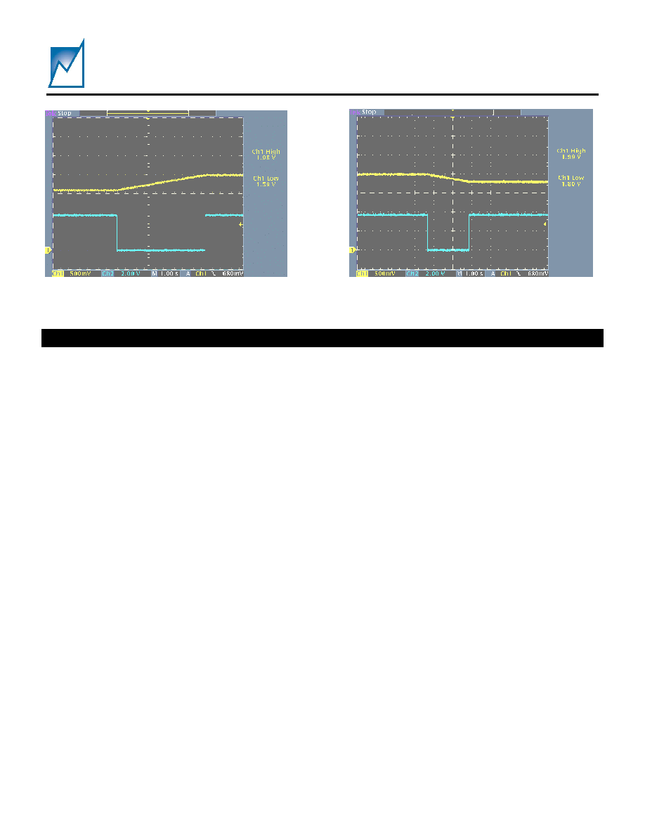
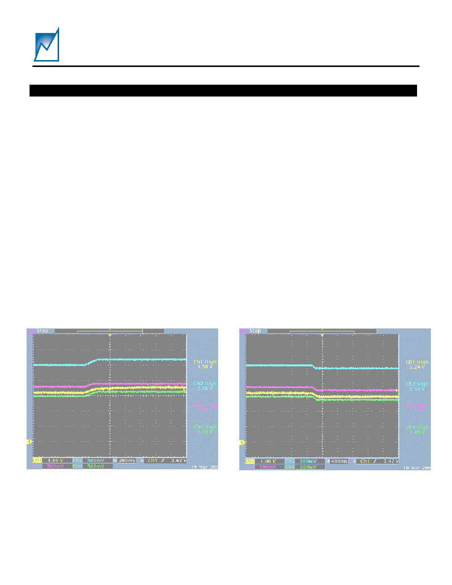
Figure 2 ≠ Example Power Supply Margining using the SMM605. The waveform on the left is margin low to
high from 1.6V to 2.0V and the waveform on the right is margin high to nominal from 2.0V to 1.8V. The ADOC
function guarantees the output level to be within ±0.2% maximum with a ±0.1% external reference. The
bottom waveform is the READY signal indicating margin is complete.
SMM605
Preliminary Information
Summit Microelectronics, Inc
2064 1.1 09/16/03
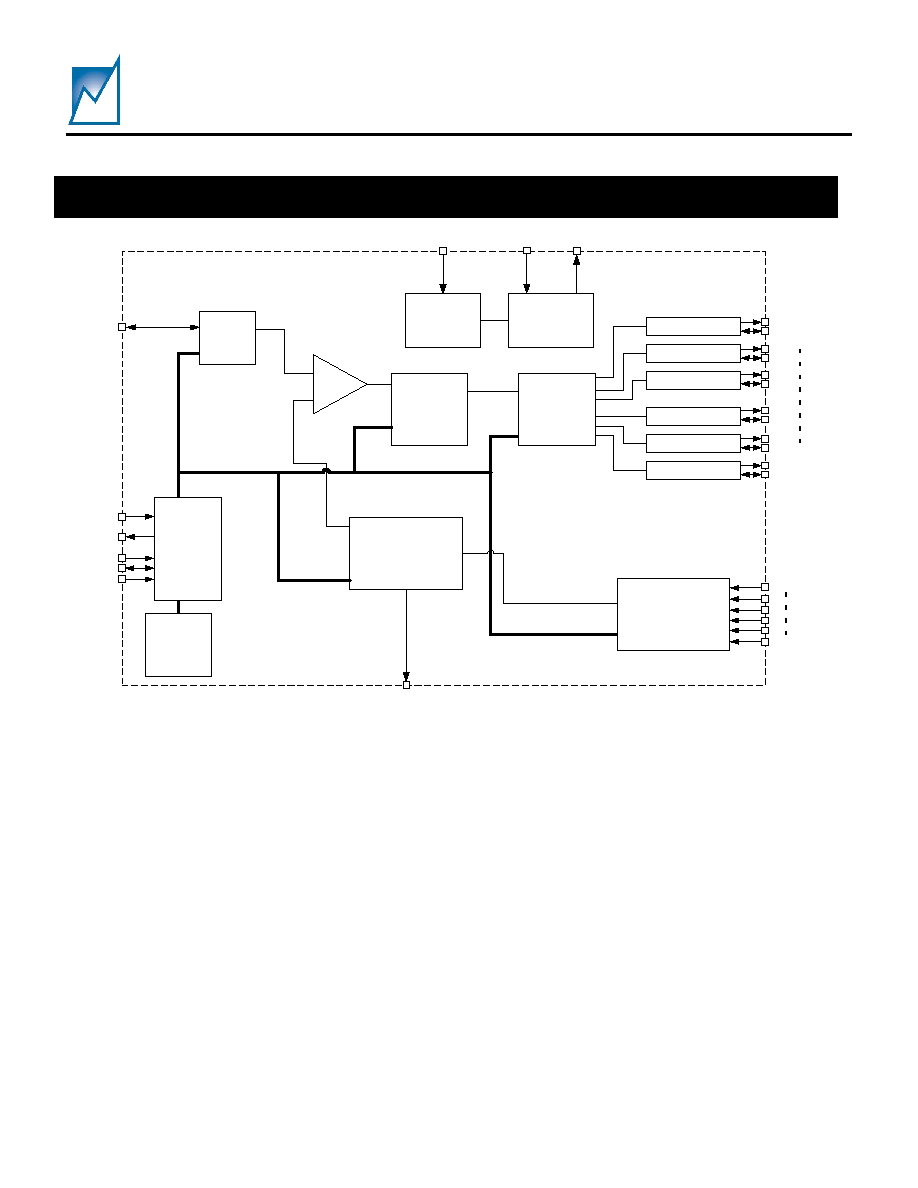
3
Output
Control
Trim Drive
Trim Drive
Trim Drive
Trim Drive
Trim Drive
Trim Drive
Input Voltage
Sensing and
Signal
Conditioning
A2
SDA
SCL
VREF_CNTL
Vout
TRIMA
TRIM_CAPA
TRIMF
TRIM_CAPF
FILT_CAP
V+
V-
VMA
VMF
READY
12VIN
VDD
3.6V or
5.5V
Regulator
Power
Supply
Arbitrator
VDD_CAP
CONTROL
LOGIC
START
1:6 MUX
6:1 MUX
Level
Shift
EE
Memory
Figure 3 ≠SMM605 Internal Functional Block Diagram.
INTERNAL FUNCTIONAL BLOCK DIAGRAM
SMM605
Preliminary Information
Summit Microelectronics, Inc
2064 1.1 09/16/03
4
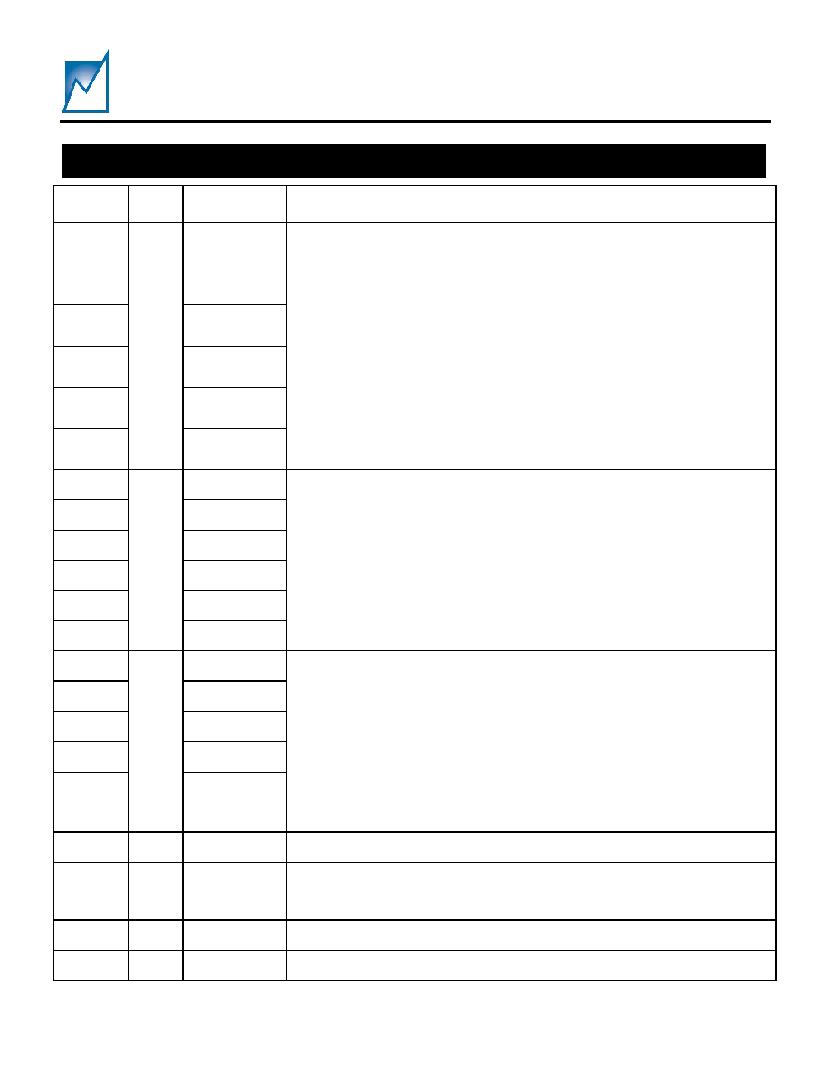
Pin
Number
1
Pin
Type
Pin Name
Pin Description
41
VM
A
36
VM
B
31
VM
C
26
VM
D
21
VM
E
16
IN
VM
F
Voltage monitor pin. Connect to the DC-DC converter + sense line or +Vout
pin.
44
TRIM
A
39
TRIM
B
34
TRIM
C
29
TRIM
D
24
TRIM
E
19
OUT
TRIM
F
Output voltage used to margin and/or trim converter voltages. Connect to the
converter Trim input or to the VADJ or FB pin of an adjustable output switching
regulator or LDO through a resistor.
45
TRIM_CAP
A
40
TRIM_CAP
B
35
TRIM_CAP
C
30
TRIM_CAP
D
25
TRIM_CAP
E
20
I/O
TRIM_CAP
F
External sample and hold capacitor input used to set the voltage on the TRIM
pins.
48
IN
VDD_CAP
External capacitor input used to filter the internal supply rail.
47
PWR
12VIN
12V power supply input internally regulated to 3.6 or 5.5V. Input range is 6V to
14V using the 3.6V internal regulator setting and 10V to 14V using the 5.5V
internal regulator setting.
46
PWR
VDD
2.7V to 5.5V Power supply of the part.
5,6,12,13 GND
GND
Ground of the part.
PIN DESCRIPTIONS
SMM605
Preliminary Information
Summit Microelectronics, Inc
2064 1.1 09/16/03
5
Pin
Number
Pin
Type
Pin Name
Pin Description
15
IN
FILT_CAP
External capacitor input used to filter VM
X
inputs. . This provides an RC filter
where R = 1k.
14
IN
VREF_CNTL
Voltage reference input used for DC output control and margining.
1
I/O
SDA
Bi-directional I
2
C data line.
2
IN
SCL
I
2
C clock line.
3
IN
A2
The address pin is biased either to VDD_CAP or GND. When
communicating with the SMM605 over the 2-wire bus A2 provides a
mechanism for assigning a unique bus address.
4
IN
START
Programmable active high/low input. The START input is used solely for
enabling Active Control and/or margining.
7
OUT
READY
Programmable active high/low open drain output signals indicating when all
programmed power supplies have reached their preprogrammed setpoints.
NC
No Connect
Leave the NC pins floating.
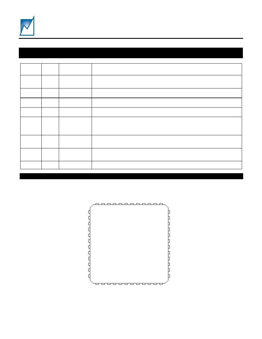
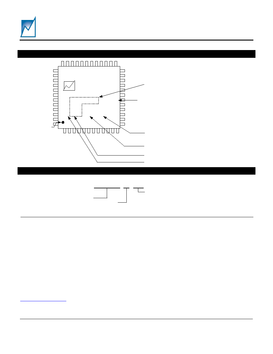
PACKAGE AND PIN CONFIGURATION
48 LEAD TQFP
1
2
3
4
5
6
7
8
9
10
11
12
13
14
15
16
17
18
19
20
21
22
23
24
36
35
34
33
32
31
30
29
28
27
26
25
48
47
46
45
44
43
42
41
40
39
38
37
SDA
SCL
A2
START
GND
GND
READY
NC
NC
NC
GND
NC
VMB
TRIMC
NC
NC
VMC
TRIMD
NC
NC
VMD
VD
D
_
C
A
P
12
V
I
N
VD
D
TRIM
_C
APA
TR
I
M
A
NC
NC
VM
A
TR
I
M
B
NC
NC
GN
D
VR
EF_
C
N
T
L
FI
LT_C
A
P
VM
F
NC
NC
TRIM
F
TR
I
M
_C
APF
VME
NC
TR
I
M
E
NC
TR
I
M
_
C
A
P
B
TRIM_CAPC
TRIM_CAPD
TRIM_CAPE
PIN DESCRIPTIONS (Cont.)
SMM605
Preliminary Information
Summit Microelectronics, Inc
2064 1.1 09/16/03
6
ABSOLUTE MAXIMUM RATINGS
Temperature Under Bias ...................... -55
∞
C to 125
∞
C
Storage Temperature............................ -65
∞
C to 150
∞
C
Terminal Voltage with Respect to GND:
VDD Supply Voltage ..........................-0.3V to 6.0V
12VIN Supply Voltage......................-0.3V to 15.0V
All Others ................................-0.3V to V
DD
+ 0.7V
Output Short Circuit Current ............................... 100mA
Lead Solder Temperature (10 secs)...................300
∞
C
Junction Temperature........................................150∞C
ESD Rating per JEDEC...............................2000V
Latch-Up testing per JEDEC........................
±
100mA
Note - The device is not guaranteed to function outside its operating
rating. Stresses listed under Absolute Maximum Ratings may cause
permanent damage to the device. These are stress ratings only and
functional operation of the device at these or any other conditions
outside those listed in the operational sections of the specification is
not implied. Exposure to any absolute maximum rating for extended
periods may affect device performance and reliability. Devices are
ESD sensitive. Handling precautions are recommended.
RECOMMENDED OPERATING CONDITIONS
Temperature Range (Industrial)...........≠40
∞
C to +85
∞
C
(Commercial) ............≠5
∞
C to +70
∞
C
VDD Supply Voltage .................................. 2.7V to 5.5V
12VIN Supply Voltage (1) ........................ 6.0V to 14.0V
VIN ............................................................ GND to VDD
VOUT ...................................................... GND to 15.0V
Package Thermal Resistance (
JA
)
48 Lead TQFP........................................80
o
C/W
Moisture Classification Level 1 (MSL 1) per J-STD- 020
Note 1 ≠ Range depends on internal regulator set to 3.6V or 5.5V,
see 12VIN specification below.
DC OPERATING CHARACTERISTICS
(Over recommended operating conditions, unless otherwise noted. All voltages are relative to GND.)
Symbol Parameter Notes
Min
Typ
Max
Unit
VDD
Supply Voltage
2.7
5.5
V
Internally regulated to 5.5V
10
14
V
12VIN Supply
Voltage
Internally regulated to 3.6V
6
14
V
I
DD
Power Supply Current from VDD
All TRIM pins floating,
12VIN floating
3
5
mA
I
12VIN
Power Supply Current from 12VIN
All TRIM pins floating,
VDD floating
3
5
mA
TRIM characteristics
TRIM Sourcing Maximum
Current
1.5
mA
I
TRIM
TRIM output current through 100
to
1.0V
TRIM Sinking Maximum
Current
1.5
mA
V
TRIM
Margin Control and ADOC Range
Depends on Trim range of
DC-DC Converter
VREF_CNTL/
4
VDD V
All other input and output characteristics
VDD = 2.7V
0.9xVDD
VDD
V
V
IH
Input High Voltage (FS,
PWR_ON/OFF, MR#, SDA, SCL)
VDD = 5.0V
0.7xVDD
VDD
V
VDD = 2.7V
-0.1
0.1xVDD
V
V
IL
Input Low Voltage (FS,
PWR_ON/OFF, MR#, SDA, SCL)
VDD = 5.0V
-0.1
0.3xVDD
V
V
OL
Programmable Open Drain Outputs
(RST, HEALTHY, FAULT, PUPx)
I
SINK
= 1mA
0
0.4
V
I
OL
Output Low Current
Note ≠ Total I
SINK
from all PUPx pins
should not exceed 3mA or ADOC
ACC
specification will be affected
0
1.0
mA
SMM605
Preliminary Information
Summit Microelectronics, Inc
2064 1.1 09/16/03
7
DC OPERATING CHARACTERISTICS
(Over recommended operating conditions, unless otherwise noted. All voltages are relative to GND.)
Symbol Parameter
Notes Min
Typ.
Max
Unit
V
SENSE
Positive Sense Voltage
VM pins
+0.35
VDD_CAP
V
V
Monitor
Monitor Threshold Step Size
VM pins
5
mV
V
REF
Internal 1.25V
REF
Output Voltage
1.24
1.25
1.26
V
≠40
∞
C to +85
∞
C
-0.25 +0.25
%
V
REF
TC
Internal V
REF
Temperature
Coefficient
≠5
∞
C to +70
∞
C
-0.15 +0.15
%
V
REF
ACC Internal V
REF
Accuracy
-0.4
+0.4
%
External
V
REF
External V
REF
Voltage Range
0.5
VDD_CAP
V
External V
REF
=1.25V, ±0.1%,
-0.2
±
0.1
+0.2 %
ADOC
ACC
ADOC/Margin
Accuracy
Internal V
REF
=1.25V
-0.5
±
0.3
+0.5 %
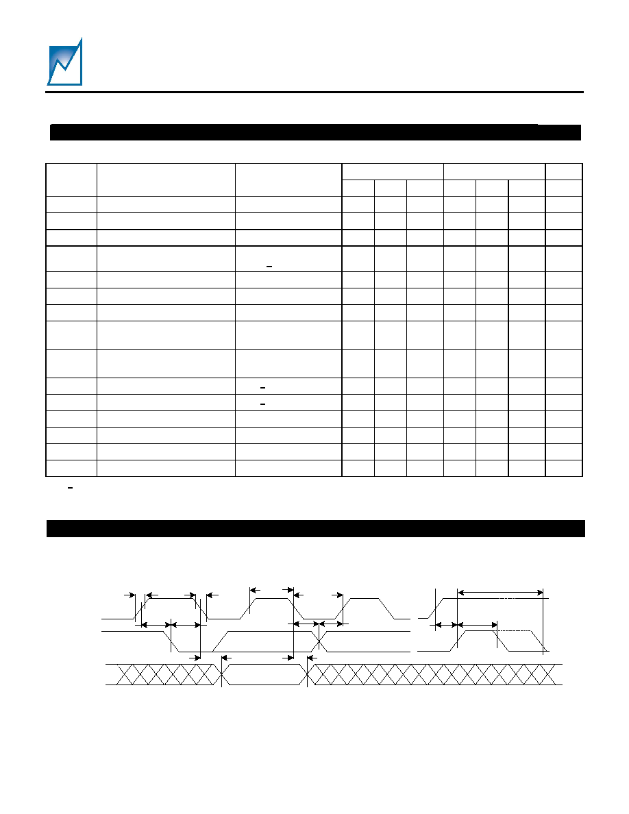
AC OPERATING CHARACTERISTICS
(Over recommended operating conditions, unless otherwise noted. All voltages are relative to GND.) See
Figure 3, 4 and 5 Timing diagrams.
Symbol Description
Conditions
Min
Typ
Max
Unit
t
DC_CONTROL
Active DC Control sampling period
Update period for Active
DC Control of channels
A ≠ F
1.7
ms
T
settling
Settling Time
+ 10% change in voltage
with 0.1% ripple
100
ms
Slow Margin,
TRIM_CAP=1
µF
100
ms
T
MARGIN
Margin Time from Nominal to
±
5%
Fast Margin,
TRIM_CAP=1
µF
1
ms
SMM605
Preliminary Information
Summit Microelectronics, Inc
2064 1.1 09/16/03
8
I
2
C 2-WIRE SERIAL INTERFACE AC OPERATING
CHARACTERISTICS ≠ 100/400kHz
Over recommended operating conditions, unless otherwise noted. All voltages are relative to GND. See Figure 4 Timing Diagram.
100kHz 400kHz
Symbol Description
Conditions
Min Typ Max Min Typ Max Units
f
SCL
SCL Clock Frequency
0 100
0 400
KHz
t
LOW
Clock Low Period
4.7 1.3 µs
t
HIGH
Clock
High
Period
4.0 0.6 µs
t
BUF
Bus Free Time
Before New Transmission
-
Note 1/
4.7 1.3 µs
t
SU:STA
Start Condition Setup Time
4.7
0.6
µs
t
HD:STA
Start Condition Hold Time
4.0
0.6
µs
t
SU:STO
Stop Condition Setup Time
4.7
0.6
µs
t
AA
Clock Edge to Data Valid
SCL low to valid
SDA (cycle n)
0.2 3.5 0.2 0.9 µs
t
DH
Data Output Hold Time
SCL low (cycle n+1)
to SDA change
0.2 0.2 µs
t
R
SCL and SDA Rise Time
Note 1/
1000
1000
ns
t
F
SCL and SDA Fall Time
Note 1/
300 300 ns
t
SU:DAT
Data In Setup Time
250
150
ns
t
HD:DAT
Data In Hold Time
0
0
ns
TI
Noise Filter SCL and SDA
Noise suppression
100
100
ns
t
WR
Write
Cycle
Time
5 5 ms
Note: 1/ - Guaranteed by Design.
t
R
t
F
t
HIGH
t
LOW
t
SU:SDA
t
HD:SDA
t
SU:DAT
t
HD:DAT
t
SU:STO
t
BUF
t
DH
t
AA
SCL
SDA
(IN)
SDA
(OUT)
t
W R (For W rite Operation Only)
Figure 4 - Basic I
2
C Serial Interface Timing
TIMING DIAGRAMS

SMM605
Preliminary Information
Summit Microelectronics, Inc
2064 1.1 09/16/03
9
APPLICATIONS INFORMATION
DEVICE OPERATION
POWER SUPPLY
The SMM605 can be powered by either an 6V to 14V
input through the 12VIN pin or by a 2.7V to 5.5V input
through the VDD pin (Figure 5). The 12VIN pin feeds
an internal programmable regulator that internally
generates either 5.5V or 3.6V. The internal regulator
must be set to 3.6V if using an 8V supply. A voltage
arbitration circuit allows the device to be powered by
the highest voltage from either the regulator output or
the VDD input. This voltage arbitration circuit
continuously checks for these voltages to determine
which will power the SMM605. The resultant internal
power supply rail is connected to the VDD_CAP pin
that allows both filtering and hold-up of the internal
power supply.
VOLTAGE REFERENCE
The SMM605 can operate using either an internal or
external voltage reference, VREF. The internal VREF
is set to 1.25V. Total accuracy with a ±0.1% external
reference is ±0.2% and ±0.5% using the internal
reference.
MODES OF OPERATION
The SMM605 has two basic modes of operation:
supply margining mode and Active DC Output Control
(ADOC
TM
). A detailed description of each mode and
feature follows.
ACTIVE DC OUTPUT CONTROL (ADOC)
The SMM605 can actively control the DC output
voltage of bricks or DC/DC converters that have a trim
pin during monitoring and margining mode. The
converter may be an off-the shelf compact device, or
may be a "roll your own" circuit on the application
board. In either case, the SMM605 dramatically
improves voltage accuracy (down to
±
0.2%) by
implementing closed-loop ADOC active control. This
utilizes the DC-DC's "trim" pin as shown in Figure 7, or
an equivalent output voltage feedback adjustment
"VADJ" or "FB" node in a user's custom circuit, Figure
8. Each of the TRIM
X
pins on the SMM605 is
connected to the trim input pins on the power supply
converters.
A sense line from the channel's point-of-load connects
to the corresponding VM
X
input. The ADOC function
cycles through all six channels (A-F) every 1.7ms
making slight adjustments to the voltage on the
associated TRIM
X
output pins based on the voltage
inputs on the VM
X
pins. These voltage adjustments
allow the SMM605 to control the output voltage of
power supply converters to within ±0.2% when using a
±0.1% external voltage reference.
The voltage on the TRIM_CAP
X
pins is buffered and
applied to the TRIM
X
pin. The voltage adjustments on
the TRIM
X
pins cause a slight ripple of less than 1mV
on the power supply voltage. The amplitude of this
ripple is a function of the TRIM_CAP
X
capacitor and
the trim gain of the converter. Calculation of the
TRIM_CAP
X
capacitor to achieve a desired minimum
ripple is detailed in Application Note 37.
The pulse of current can be increased to a 10X pulse
of current until the power supply voltages are at their
nominal settings by selecting the programmable Fast
Convergence option. As the name implies, this option
decreases the time required to bring a supply voltage
from the converter's nominal output voltage to the
Active DC Output Control nominal voltage setting.
The device can be programmed to either enable or
disable the Active DC Control function. When
disabled or not active, the TRIM
X
pins on the SMM605
are high impedance inputs. The voltage on the TRIM
X
pins are buffered and applied to the TRIM_CAP
X
pins
charging the capacitor. This allows a smooth
transition from the converter's nominal voltage to the
SMM605 controlling that voltage to the Active DC
Control nominal setting.
MONITORING
The SMM605 monitors the VM
X
pins. The READY pin
is programmable active high/low open drain output
indicates that all VM
X
pins are at their set point.
SMM605
Preliminary Information
Summit Microelectronics, Inc
2064 1.1 09/16/03
10
MARGINING
The SMM605 has two additional Active DC Output
Control voltage settings: margin high and margin low.
The margin high and margin low settings can be as
much as
±10% of the nominal setting depending on
the manufacturer. The SMM605 range can be as
large as 0.35V to VDD. These settings are stored in
the configuration registers and are loaded into the
Active DC Output Control voltage setting by margin
commands issued via the I
2
C bus. The device must
be enabled for Active DC Output Control in order to
enable margining.
The margin command registers contain two bits that
decode the commands to margin high, margin low, or
control to the nominal setting. Once the SMM605
receives the command to margin the supply voltage, it
begins adjusting the supply voltage to move toward
the desired setting. When this voltage setting is
reached, a bit is set in the margin status registers and
the READY signal becomes active. (Figure 2, 5 and 6)
Note: Configuration writes or reads of registers 00
HEX
to 03
HEX
should not be performed while the SMM605 is
margining.
WRITE PROTECTION
Write protection for the SMM605 is located in a volatile
register where the power-on state is defaulted to write
protect. There are separate write protect modes for the
configuration registers and memory. In order to
remove write protection, the code 55
HEX
is written to
the write protection register. Other codes will enable
write protection. For example, writing 59
HEX
will allow
writes to the configuration register but not to the
memory, while writing 35
HEX
will allow writes to the
memory but not to the configuration registers. In
addition, there is a configuration register lock bit
which, once programmed, does not allow the
configuration registers to be changed.
Figure 5 - Margin High Waveforms
Time/Horizontal division = 200mS
Ch 1 (1V/Div) = 3.3V DC-DC converter output (Yellow trace)
Ch 2 (500mV/Div) = 2.5VDC-DC converter output (Blue trace)
Ch 3 (500mV/Div) = 1.8V DC-DC converter output (Purple trace)
Ch 4 (500mV/Div) = 1.5V DC-DC converter output (Green trace)
Figure 6 - Margin Low Waveforms
Time/Horizontal division = 400mS
Ch 1 (1V/Div) = 3.3V DC-DC converter output (Yellow trace)
Ch 2 (500mV/Div) = 2.5V DC-DC converter output (Blue trace)
Ch 3 (500mV/Div) = 1.8V DC-DC converter output (Purple trace)
Ch 4 (500mV/Div) = 1.5V DC-DC converter output (Green trace)
APPLICATIONS INFORMATION (CONTINUED)
SMM605
Preliminary Information
Summit Microelectronics, Inc
2064 1.1 09/16/03
11
READY
START
J1
Ext VRef
C6 1uF
R4 10K
R1 10K
J1
1
2
3
4
5
6
7
8
9
10
Gnd
SCL
Gnd3
SDA
Rsrv5
MR
+10V
Rsrv8
+5V
Rsrv10
R2 10K
C6
0.1uF
C8
0.1uF
The SMM605 and the DC-DC Converter
Can Operate with either 12V or VDD
If 12V is used, VDD can be left floating
If VDD is used, 12V can be left floating
D1
DIODE
If the SMM605 internal VREF
is used, the VREF_CNTL pin
becomes an output
C4
0.1uF
DC-DC ENABLE
+12VIN (+6V to +14V)
SMX3200 I2C
Programming
Connector 10
pin Header
C1
0.1uF
C2
0.1uF
R3 10K
U4
LM4121
1
2
3
4
5
Ref
Gnd EN
VIn
VOut
C5
0.02uF
U1
SMM605
2
3
4
7
14
15
46
47
48
1
6
5
12
13
SCL
A2
START
READY
VREF_CNTL
FILT_CAP
VMX
TRIM_CAPX
TRIMX
VDD
12VI
N
VDD_CAP
SDA
GND
GND
GND
GND
Vdd
U2
DC-DC Converter
1
2
3
4
5
6
7
8
9
10
11
+Vout
+Vout
Sense
+Vout
Gnd Gnd
+Vin
+Vin
+Vin
Trim
Enable
C3
0.01uF
VDD (+2.7V to +5.5V)
VOUT
J2
Supply
C7
0.01uF
Figure 7 ≠ SMM605 Applications schematic. The accuracy of the external (U4) or internal reference sets the
accuracy of the ADOC function. Total accuracy with a ±0.1% external reference is ±0.2% and ±0.5% with the
internal reference. The 12V supply can go as low as 6V if the internal regulator is set to 3.6V.
APPLICATIONS INFORMATION (CONTINUED)
SMM605
Preliminary Information
Summit Microelectronics, Inc
2064 1.1 09/16/03
12
U2
LT3707 Switching Regulator
+Vout
Gnd
+Vin
VOSENSE
PGOOD
U1
SMM605
2
3
4
7
14
15
46
47
48
1
6
5
12 13
SCL
A2
START
READY
VREF
_CNT
L
FILT_CAP
VMX
TRIM_CAPX
TRIMX
VDD
12VI
N
VDD_CAP
SDA
GND
GND
GND GND
START
C1 should be as close
to the SMM105 as
possible
C2
0.02uF
R4 10K
C4
0.1uF
D1
DIODE
C6
0.01uF
The SMM605 START pin must be inactive during power-up so
that the TRIM pin is high impedence. Once power is nominal,
the START pin can be active to start margin and ADOC
functions
R5
20k
R2 10K
C1 1uF
J1
1
2
3
4
5
6
7
8
9
10
Gnd
SCL
Gnd3
SDA
Rsrv5
MR
+10V
Rsrv8
+5V
Rsrv10
C3
0.1uF
R5 10K
START
R4
RSET1
VOUT
VTRIMlow=0.3V, VOSENSE=0.8V
The current through R3 is
ITRIM=(0.8-0.3)/RTRIM
(ITRIM)(R4) > 15% of VOUT
RTRIMmax should be no greater
then the calculated value
READY
For Example, If Vout=3.3V, R4=63.4K
15% of Vout=0.5V
ITRIM=8uA
RTRIM=62.5K so Rtrim should be
next value down from 62.5K
C5
0.01uF
R3 RTRIM
+12VIN(+6V to 14V)
SMX3200 I2C Programming
Connector 10 pin Header
R1 and R2 need only be
placed once on the I2C bus
R1 10K
Figure 8 ≠ SMM605 Applications schematic for an adjustable switching regulator (Full regulator circuit not
shown).
APPLICATIONS INFORMATION (CONTINUED)
SMM605
Preliminary Information
Summit Microelectronics, Inc
2064 1.1 09/16/03
13
Figure 9 ≠ SMM605 Applications schematic.
APPLICATIONS INFORMATION (CONTINUED)
SMM605
Preliminary Information
Summit Microelectronics, Inc
2064 1.1 09/16/03
14
The end user can obtain the Summit SMX3200
programming system for device prototype
development. The SMX3200 system consists of a
programming Dongle, cable and Windows
TM
GUI
software. It can be ordered on the website or from a
local representative. The latest revisions of all
software and an application brief describing the
SMX3200 is available from the website
(
www.summitmicro.com
).
The SMX3200 programming Dongle/cable interfaces
directly between a PC's parallel port and the target
application. The device is then configured on-screen
via an intuitive graphical user interface employing
drop-down menus.
The Windows GUI software will generate the data and
send it in I
2
C serial bus format so that it can be directly
downloaded to the SMM605 via the programming
Dongle and cable. An example of the connection
interface is shown in Figure 10.
When design prototyping is complete, the software
can generate a HEX data file that should be
transmitted to Summit for approval. Summit will then
assign a unique customer ID to the HEX code and
program production devices before the final electrical
test operations. This will ensure proper device
operation in the end application.
Pin 9, 5V
Pin 7, 10V
Pin 5, Reserved
Pin 3, GND
Pin 1, GND
Pin 6, MR#
Pin 4, SDA
Pin 2, SCL
Pin 8, Reserved
Pin 10, Reserved
Top view of straight 0.1" x 0.1 closed-side
connector. SMX3200 interface cable connector.
9
7
5
3
1
10
8
6
4
2
SMM605
SDA
SCL
VDD_CAP
GND
0.1
F
Positive
Supply
Common
Ground
D1
1N4148
Figure 10≠ SMX3200 Programmer I
2
C serial bus connections to program the SMM605. The SMM605 has a
Write Protect pin (WP# input) which when, asserted, prevents writing to the configuration registers and EE
memory. In addition, there is a configuration register lock bit which, once programmed, does not allow the
configuration registers to be changed.
DEVELOPMENT HARDWARE & SOFTWARE

SMM605
Preliminary Information
Summit Microelectronics, Inc
2064 1.1 09/16/03
15
SERIAL INTERFACE
Access to the configuration registers, general-purpose
memory and command and status registers is carried
out over an industry standard 2-wire serial interface
(I
2
C). SDA is a bi-directional data line and SCL is a
clock input. Data is clocked in on the rising edge of
SCL and clocked out on the falling edge of SCL. All
data transfers begin with the MSB. During data
transfers SDA must remain stable while SCL is high.
Data is transferred in 8-bit packets with an intervening
clock period in which an Acknowledge is provided by
the device receiving data. The SCL high period (t
HIGH
)
is used for generating Start and Stop conditions that
precede and end most transactions on the serial bus.
A high-to-low transition of SDA while SCL is high is
considered a Start condition while a low-to-high
transition of SDA while SCL is high is considered a
Stop condition.
The interface protocol allows operation of multiple
devices and types of devices on a single bus through
unique device addressing. The address byte is
comprised of a 4-bit device type identifier (slave
address) and a 3-bit bus address. The remaining bit
indicates either a read or a write operation. Refer to
Table 1 for a description of the address bytes used by
the SMM605.
The device type identifier for the memory array is
generally set to 1010
BIN
following the industry standard
for a typical nonvolatile memory. There is an option to
change the identifier to 1011
BIN
allowing it to be used
on a bus that may be occupied by other memory
devices. The configuration registers are grouped with
the memory array and thus use 1010
BIN
or 1011
BIN
as
the device type identifier. The command and status
registers are accessible with the separate device type
identifier of 1001
BIN
.
The bus address bits A[1:0] are programmed into the
configuration registers. Bus address bit A[2] can be
programmed as either 0 or biased by the A2 pin. The
bus address accessed in the address byte of the serial
data stream must match the setting in the SMM605
and on the A2 pin.
Any access to the SMM605 on the I
2
C bus will
temporarily halt the monitoring function. The SMM605
halts the monitor function from when it acknowledges
the address byte until a valid stop is received.
WRITE
Writing to the memory or a configuration register is
illustrated in Figures 11, 12, 13, 17 and 18. A Start
condition followed by the address byte is provided by
the host; the SMM605 responds with an Acknowledge;
the host then responds by sending the memory
address pointer or configuration register address
pointer; the SMM605 responds with an acknowledge;
the host then clocks in on byte of data. For memory
and configuration register writes, up to 15 additional
bytes of data can be clocked in by the host to write to
consecutive addresses within the same page. After
the last byte is clocked in and the host receives an
Acknowledge, a Stop condition must be issued to
initiate the nonvolatile write operation.
READ
The address pointer for the configuration registers,
memory, command and status registers must be set
before data can be read from the SMM605. This is
accomplished by issuing a dummy write command,
which is simply a write command that is not followed
by a Stop condition. The dummy write command sets
the address from which data is read. After the dummy
write command is issued, a Start command followed
by the address byte is sent from the host. The host
then waits for an Acknowledge and then begins
clocking data out of the slave device. The first byte
read is data from the address pointer set during the
dummy write command. Additional bytes can be
clocked out of consecutive addresses with the host
providing an Acknowledge after each byte. After the
data is read from the desired registers, the read
operation is terminated by the host holding SDA high
during the Acknowledge clock cycle and then issuing a
Stop condition. Refer to Figures 14, 16, 19 and 21 for
an illustration of the read sequence.
I
2
C PROGRAMMING INFORMATION
SMM605
Preliminary Information
Summit Microelectronics, Inc
2064 1.1 09/16/03
16
WRITE PROTECTION
The SMM605 powers up into a write protected mode.
Writing a code to the volatile write protection register
can disable the write protection. The write protection
register is located at address 87
HEX
of slave address
1001
BIN
.
Writing 0101
BIN
to bits [7:4] of the write protection
register allow writes to the general-purpose memory
while writing 0101
BIN
to bits [3:0] allow writes to the
configuration registers. The write protection can re-
enable by writing other codes (not 0101
BIN
) to the write
protection register. Writing to the write protection
register is shown in Figure 11.
CONFIGURATION REGISTERS
The majority of the configuration registers are grouped
with the general-purpose memory located at either
slave address 1010
BIN
or 1011
BIN
. The bus address
bits, A[1:0], used to differentiate the general-purpose
memory from the configuration registers are set to
11
BIN
. Bus address bit A[2] can be programmed as
either 0 or biased by the A2 pin.
Two additional configuration registers are located at
addresses 83
HEX
and 84
HEX
of slave address 1001
BIN
.
Writing and reading the configuration registers is
shown in Figures 14 and 16.
Note: Configuration writes or reads of registers 00
HEX
to 0F
HEX
should not be performed while the SMM605 is
margining.
GENERAL-PURPOSE MEMORY
The 4k-bit general-purpose memory is located at
either slave address 1010
BIN
or 1011
BIN
. The bus
address bits, A[1:0], used to differentiate the general-
purpose memory from the configuration registers are
set to 00
BIN
for the first 2k-bits and 01
BIN
for the second
2k-bits. Bus address bit A[2] can be programmed as
either 0 or biased by the A2 pin.
The word address must be set each time the memory
is accessed. Memory writes and reads are shown in
Figures 17, 18 and 19.
COMMAND AND STATUS REGISTERS
The command and status registers are located at
slave address 1001
BIN
. Writes and reads of the
command and status registers are shown in Figures
20 and 21.
GRAPHICAL USER INTERFACE (GUI)
Device configuration utilizing the Windows based
SMM605 graphical user interface (GUI) is highly
recommended. The software is available from the
Summit website (
www.summitmicro.com
). Using the
GUI in conjunction with this datasheet and application
note 40 simplifies the process of device prototyping
and the interaction of the various functional blocks. A
programming Dongle (SMX3200) is available from
Summit to communicate with the SMM605. The
Dongle connects directly to the parallel port of a PC
and programs the device through a cable using the I
2
C
bus protocol.
Slave Address Bus Address Register Type
1001
BIN
A2 A1 A0
Write Protection Register,
Command and Status Registers,
Two Configuration Registers
A2 0 0
1
st
2-k Bits of General-Purpose Memory
A2 0 1
2
nd
2-k Bits of General-Purpose Memory
1010
BIN
or
1011
BIN
A2 1 1
Configuration Registers
Table 1 - Address bytes used by the SMM605.
I
2
C PROGRAMMING INFORMATION (CONTINUED)
SMM605
Preliminary Information
Summit Microelectronics, Inc
2064 1.1 09/16/03
17
S
T
A
R
T
W
A
C
K
M aster
Slave
A
C
K
Configuration
Register Address = 87
HEX
1
0
0
0
0
1
1
1
0
1
0
1
0
1
0
1
S
T
O
P
Data = 55
HEX
A
C
K
1
0
0
1
A
2
Bus Address
A
1
A
0
5
HEX
Unlocks
General Purpose
EE
5
HEX
Unlocks
Configuration
Registers
W rite Protection
Register Address
8
HEX
7
HEX
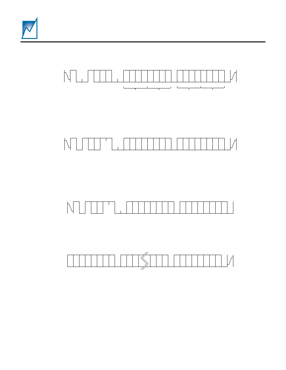
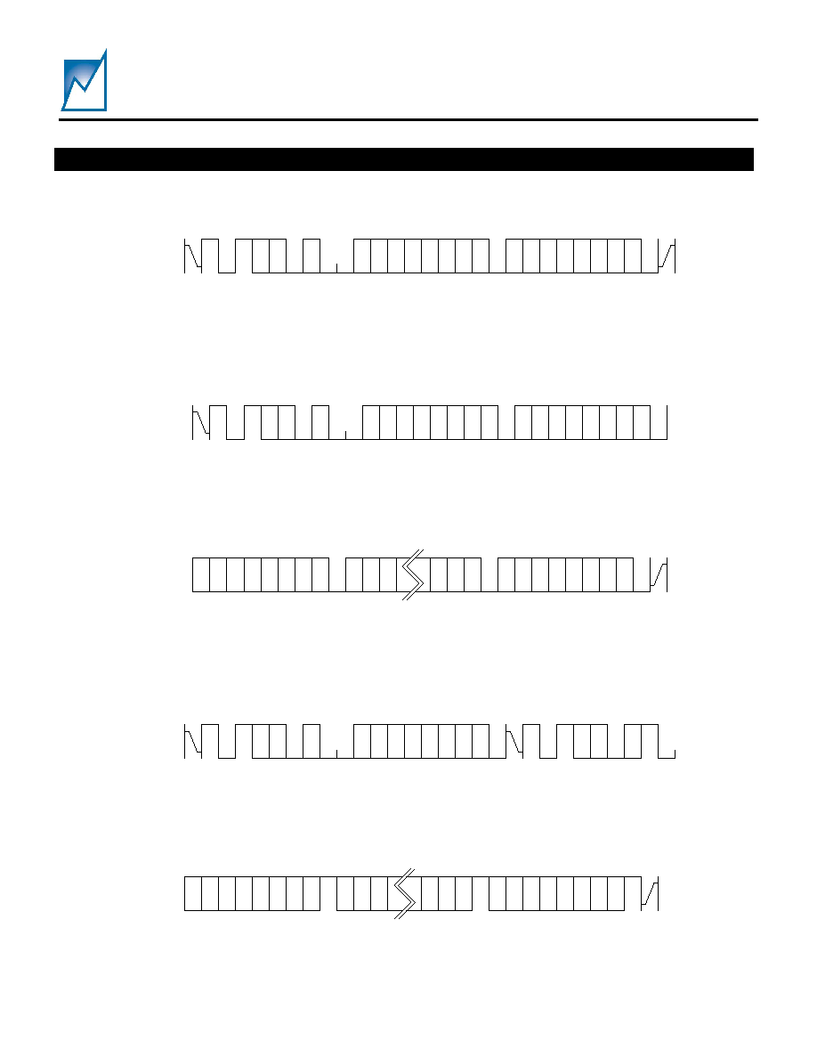
Figure 11 ≠ Write Protection Register Write
S
T
A
R
T
1
A
2
Bus Address
W
A
C
K
Master
Slave
A
C
K
1
1
0
1
S
A
0
Configuration
Register Address
C
7
C
6
C
5
C
4
C
3
C
2
C
1
C
0
D
7
D
6
D
5
D
4
D
3
D
2
D
1
D
0
S
T
O
P
Data
A
C
K
Figure 12 ≠ Configuration Register Byte Write
S
T
A
R
T
1
A
2
Bus Address
W
A
C
K
D
7
D
6
D
5
D
4
D
3
D
2
D
1
D
0
S
T
O
P
Master
Master
Slave
Slave
A
C
K
Data (16)
1
1
0
1
S
A
0
Configuration
Register Address
C
7
C
6
C
5
C
4
C
3
C
2
C
1
C
0
A
C
K
D
7
D
6
D
5
D
4
D
3
D
2
D
1
D
0
Data (1)
A
C
K
D
7
D
6
D
5
D
4
D
3
D
2
D
1
D
0
Data (2)
A
C
K
D
7
D
6
D
5
D
2
D
1
D
0
A
C
K
Figure 13 ≠ Configuration Register Page Write
SMM605
Preliminary Information
Summit Microelectronics, Inc
2064 1.1 09/16/03
18
S
T
A
R
T
1
A
2
Bus Address
W
A
C
K
D
7
D
6
D
5
D
4
D
3
D
2
D
1
D
0
S
T
O
P
N
A
C
K
Master
Master
Slave
Slave
A
C
K
Data (n)
1
1
0
1
S
A
0
Configuration
Register Address
C
7
C
6
C
5
C
4
C
3
C
2
C
1
C
0
S
T
A
R
T
1
R
A
C
K
A
2
Bus Address
1
1
S
A
0
0
1
A
C
K
D
7
D
6
D
5
D
2
D
1
D
0
A
C
K
D
7
D
6
D
5
D
4
D
3
D
2
D
1
D
0
Data (1)
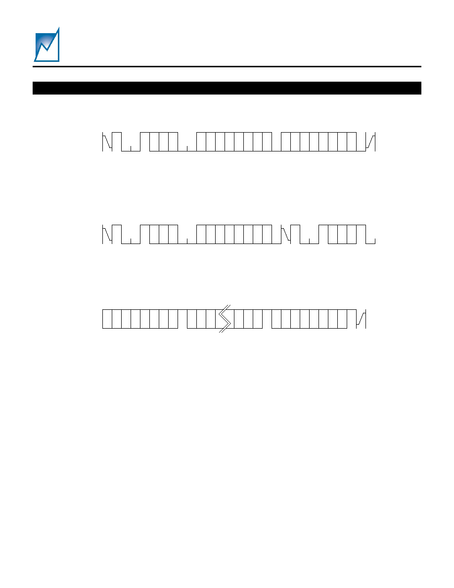
Figure 14 - Configuration Register Read
S
T
A
R
T
W
A
C
K
Master
Slave
A
C
K
Configuration
Register Address
C
7
C
6
C
5
C
4
C
3
C
2
C
1
C
0
D
7
D
6
D
5
D
4
D
3
D
2
D
1
D
0
S
T
O
P
Data
A
C
K
1
0
0
1
A
2
Bus Address
A
1
A
0
Figure 15 - Configuration Register with Slave Address 1001
BIN
Write
S
T
A
R
T
W
A
C
K
D
7
D
6
D
5
D
4
D
3
D
2
D
1
D
0
S
T
O
P
N
A
C
K
Master
Master
Slave
Slave
A
C
K
Data (n)
Configuration
Register Address
C
7
C
6
C
5
C
4
C
3
C
2
C
1
C
0
S
T
A
R
T
R
A
C
K
A
C
K
D
7
D
6
D
5
D
2
D
1
D
0
A
C
K
D
7
D
6
D
5
D
4
D
3
D
2
D
1
D
0
Data (1)
1
0
0
1
A
2
Bus Address
A
1
A
0
1
0
0
1
A
2
Bus Address
A
1
A
0
Figure 16 - Configuration Register with Slave Address 1001
BIN
Read
I
2
C PROGRAMMING INFORMATION (CONTINUED)
SMM605
Preliminary Information
Summit Microelectronics, Inc
2064 1.1 09/16/03
19
S
T
A
R
T
1
Bus Address
W
A
C
K
Master
Slave
A
C
K
0
1
S
A
0
Configuration
Register Address
C
7
C
6
C
5
C
4
C
3
C
2
C
1
C
0
D
7
D
6
D
5
D
4
D
3
D
2
D
1
D
0
S
T
O
P
Data
A
C
K
0
A
2
0
/
1
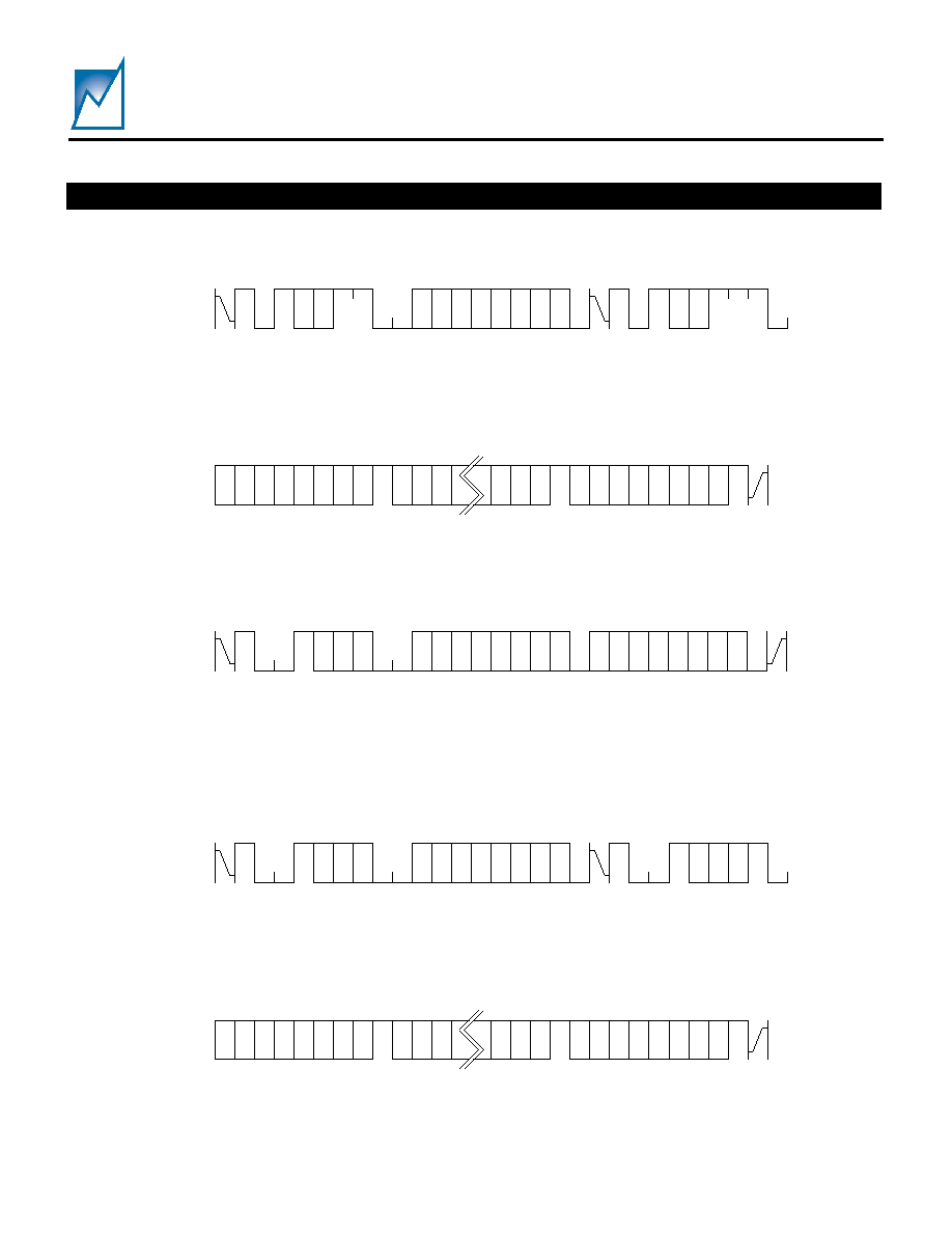
Figure 17 ≠ General Purpose Memory Byte Write
Bus Address
0
A
2
0
/
1
S
T
A
R
T
1
W
A
C
K
D
7
D
6
D
5
D
4
D
3
D
2
D
1
D
0
S
T
O
P
Master
Master
Slave
Slave
A
C
K
Data (16)
0
1
S
A
0
Configuration
Register Address
C
7
C
6
C
5
C
4
C
3
C
2
C
1
C
0
A
C
K
D
7
D
6
D
5
D
4
D
3
D
2
D
1
D
0
Data (1)
A
C
K
D
7
D
6
D
5
D
4
D
3
D
2
D
1
D
0
Data (2)
A
C
K
D
7
D
6
D
5
D
2
D
1
D
0
A
C
K
Figure 18 - General Purpose Memory Page Write
S
T
A
R
T
1
W
A
C
K
D
7
D
6
D
5
D
4
D
3
D
2
D
1
D
0
S
T
O
P
N
A
C
K
Master
Master
Slave
Slave
A
C
K
Data (n)
0
1
S
A
0
Configuration
Register Address
C
7
C
6
C
5
C
4
C
3
C
2
C
1
C
0
S
T
A
R
T
1
R
A
C
K
1
S
A
0
0
A
C
K
D
7
D
6
D
5
D
2
D
1
D
0
A
C
K
D
7
D
6
D
5
D
4
D
3
D
2
D
1
D
0
Data (1)
Bus Address
0
A
2
0
/
1
Bus Address
0
A
2
0
/
1
Figure 19 - General Purpose Memory Read
I
2
C PROGRAMMING INFORMATION (CONTINUED)
SMM605
Preliminary Information
Summit Microelectronics, Inc
2064 1.1 09/16/03
20
S
T
A
R
T
W
A
C
K
Master
Slave
A
C
K
Command and Status
Register Address
C
7
C
6
C
5
C
4
C
3
C
2
C
1
C
0
D
7
D
6
D
5
D
4
D
3
D
2
D
1
D
0
S
T
O
P
Data
A
C
K
1
0
0
1
A
2
Bus Address
A
1
A
0
Figure 20 ≠ Command and Status Register Write
S
T
A
R
T
W
A
C
K
D
7
D
6
D
5
D
4
D
3
D
2
D
1
D
0
S
T
O
P
N
A
C
K
Master
Master
Slave
Slave
A
C
K
Data (n)
Command and Status
Register Address
C
7
C
6
C
5
C
4
C
3
C
2
C
1
C
0
S
T
A
R
T
R
A
C
K
A
C
K
D
7
D
6
D
5
D
2
D
1
D
0
A
C
K
D
7
D
6
D
5
D
4
D
3
D
2
D
1
D
0
Data (1)
1
0
0
1
A
2
Bus Address
A
1
A
0
1
0
0
1
A
2
Bus Address
A
1
A
0
Figure 21 - Command and Status Register Read
I
2
C PROGRAMMING INFORMATION (CONTINUED)
SMM605
Preliminary Information
Summit Microelectronics, Inc
2064 1.1 09/16/03
21
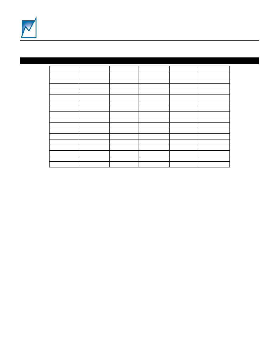
DEFAULT CONFIGURATION REGISTER SETTINGS ≠ SMM605F-186
Register Contents Register Contents Register Contents
R00 0D R18 34 R40 0D
R01
84 R19
00 R41
AB
R02 0E R30 0D R42 0E
R03
00 R31
64 R43
2D
R04 0E R32 0D R44 0E
R05 80 R33 DA R45 C7
R06
0E R34
0E R46
0E
R07 C7 R35 46 R47 F1
R08 0F R36 0E R48 0F
R09 55 R37 A2 R49 92
R0A 0B R38 0F R4A 0B
R0B
27 R39
20 R4B
70
R0C
3F R3A
0F R83
05
R0D 3F R3B D9 R84 00
R0E
04 R3C
00 R86
12
R0F
01 R3D
12 R87
F6
R3E
12
RC1
The default device ordering number is SMM605N-186, is programmed as described above
and tested over the commercial temperature range. Application Note 40 contains a
complete description of the Windows GUI and the default settings of each of the 48
individual Configuration Registers.
SMM605
Preliminary Information
Summit Microelectronics, Inc
2064 1.1 09/16/03
22
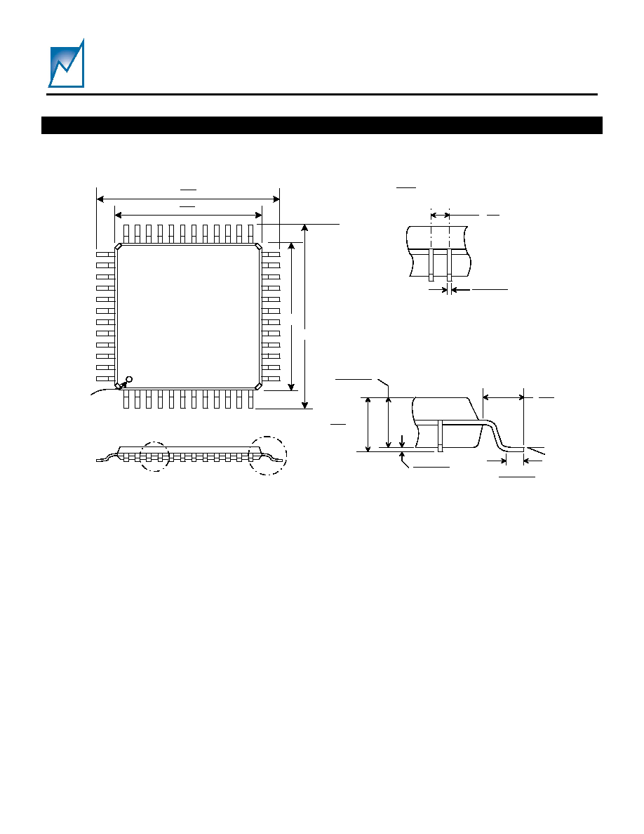
PACKAGE
A
B
Pin 1
Indicator
Inches
(Millimeters)
0.002 - 0.006
(0.05-0.15)
MAX.
0.047
(1.2)
0.037 - 0.041
0.95 - 1.05
0.018 - 0.030
(0.45 - 0.75)
0.039
(1.00)
0.02
(0.5)
BSC
0.007 - 0.011
(0.17 - 0.27)
DETAIL "A"
DETAIL "B"
(B)
(A)
(A)
0.354
(9.00) BSC
0.276
(7.00)
BSC (B)
48 PIN TQFP PACKAGE
0
o
Min to
7
o
Max
Ref Jedec M S-026
Ref
SMM605
Preliminary Information
Summit Microelectronics, Inc
2064 1.1 09/16/03
23
PART MARKING
SUMMIT
SMM605F
AYYWW
Pin 1
Annn
Summit Part Number
Date Code (YYWW)
Part Number suffix
(Contains Customer specific ordering requirements)
Lot tracking code (Summit use)
Drawing not to scale
xx
Status Tracking Code
(Blank, MS, ES, 01, 02,...)
(Summit Use)
Product Tracking Code (Summit use)
ORDERING INFORMATION
NOTICE
NOTE 1 - This is a Preliminary Information data sheet that describes a Summit product currently in pre-production with limited characterization.
SUMMIT Microelectronics, Inc. reserves the right to make changes to the products contained in this publication in order to improve design,
performance or reliability. SUMMIT Microelectronics, Inc. assumes no responsibility for the use of any circuits described herein, conveys no license
under any patent or other right, and makes no representation that the circuits are free of patent infringement. Charts and schedules contained
herein reflect representative operating parameters, and may vary depending upon a user's specific application. While the information in this
publication has been carefully checked, SUMMIT Microelectronics, Inc. shall not be liable for any damages arising as a result of any error or
omission.
SUMMIT Microelectronics, Inc. does not recommend the use of any of its products in life support or aviation applications where the failure or
malfunction of the product can reasonably be expected to cause any failure of either system or to significantly affect their safety or effectiveness.
Products are not authorized for use in such applications unless SUMMIT Microelectronics, Inc. receives written assurances, to its satisfaction, that:
(a) the risk of injury or damage has been minimized; (b) the user assumes all such risks; and (c) potential liability of SUMMIT Microelectronics, Inc.
is adequately protected under the circumstances.
Revision 1.1 - This document supersedes all previous versions. Please check the Summit Microelectronics Inc. web site at
www.summitmicro.com
for data sheet updates.
© Copyright 2003 SUMMIT MICROELECTRONICS, Inc.
Power Management for CommunicationsTM
ADOC
TM
is a trademark of Summit Microelectronics, Inc., I2C is a trademark of Philips Corporation.
SMM605
F nnn
Package
F=48 Lead TQFP
Part Number Suffix (see page 23)
Summit Part Number
Specific requirements are contained in the suffix
such as Commercial or Industrial Temp Range,
Hex code, Hex code revision, etc.