SMM764
Preliminary Information
1
(See Last Page)
© SUMMIT Microelectronics, Inc.
2004 ∑ 1717 Fox Drive ∑ San Jose CA 95131 ∑ Phone 408 436-9890 ∑ FAX 408 436-9897
The Summit Web Site can be accessed by "right" or "left" mouse clicking on the link:
http://www.summitmicro.com/
2098 1.1 6/29/2005
1
Four-Channel Active DC Output Controller, Monitor, Marginer and Sequencer with Sequence-Link
∑ Extremely accurate (±0.2%) output voltages
using Active DC Output Control (ADOCTM)
∑ Sequence-LinkTM provides sequencing of up to
46 channels
∑ ADOC automatically adjusts supply output
voltage level under all DC load conditions
∑ Monitors, controls and margins up to 4 supplies
from 0.3V to 5.5V
∑ Programmable power-on/-off sequencing
∑ Operates from any intermediate bus supply
from 6V to 14V and from 2.7V to 5.5V
∑ Monitors 12V input VDD and temperature sensor
∑ Wide margin/ADOC range from 0.3v to VDD
∑ Monitors two general-purpose 10-bit ADC inputs
∑ I
2
C 2-wire serial bus for programming
configuration and monitoring status, including
10-bit ADC conversion results
∑ 2 programmable Under Voltage (UV) and Over
Voltage (OV) threshold limits for each of 9
monitored inputs
∑ 2k-bit general purpose nonvolatile memory
Applications
∑ Monitor/control distributed and POL supplies
∑ Multi-voltage processors, DSPs, ASICSs used in
telecom, CompactPCI or server systems
The SMM764 is an Active DC Output power supply
Controller (ADOC
TM
) that monitors, margins, and
cascade sequences. The ADOC feature is unique and
maintains extremely accurate settings of system
supply voltages to within ±0.2% under full load. The
SMM764 actively controls up to 4 DC/DC converters
and can be linked with up to 7 other Sequence-LinkTM
devices to accommodate sequencing of up to 46
channels. Control of the DC-DC converters is
accomplished through the use of a Trim or Regulator
VADJ/FB pin to adjust the output voltage. For system
test, the part also controls margining of the supplies
using I
2
C commands. It can margin supplies with
either positive or negative control within a range of
0.3V to VDD, depending on the specified range of the
converter. The SMM764 also intelligently sequences
or cascades the power supplies on and off in any
order using enable outputs with programmable
polarity. It can operate off any intermediate bus supply
ranging from 6V to 14V or from 5.5V to as low as 2.7V.
The part monitors 4 power supply channels as well as
VDD, 12V input, two general-purpose analog inputs
and an internal temperature sensor using a 10-bit
ADC. The 10-bit ADC can measure the value on any
one of the monitor channels and output the data via
the I
2
C bus. A host system can communicate with the
SMM764 status register, margining and utilize 2K-bits
of nonvolatile memory.
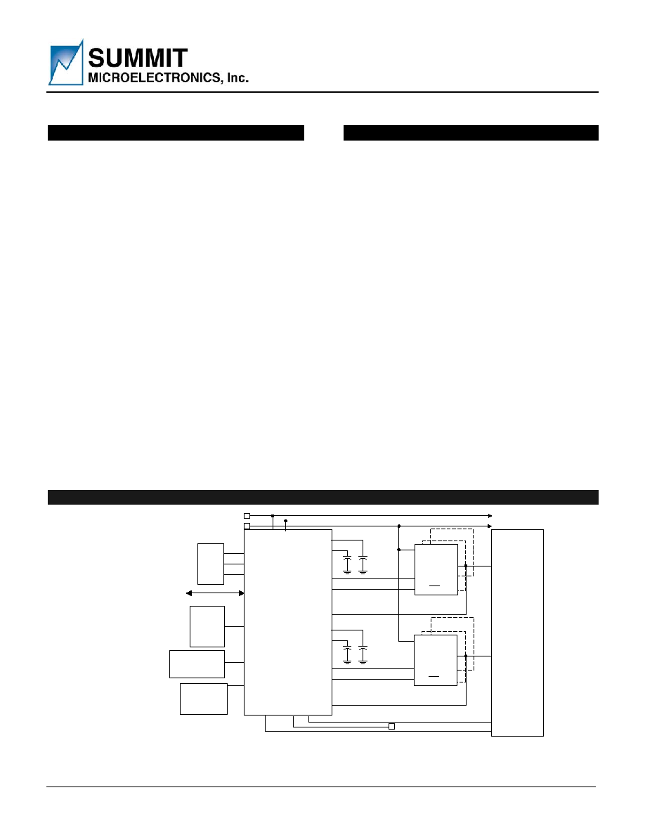
SIMPLIFIED APPLICATIONS DRAWING
TRIM
B
PUP
B
VM
B
TRIM_CAP
B
CAP
B
TRIM
A
PUP
A
VM
A
TRIM_CAP
A
CAP
A
SMM764
µP/
ASIC
VD
D
RS
T#
HE
ALT
H
Y
MR#
3.3VIN (+2.7V to +5.5V Range)
RESET#
READY
HEALTHY
12
VIN
12VIN (+6V to +14V Range)
External
or
Internal
TEMP
SENSOR
AIN1
2.5VIN
1.2VIN
12V
SDA
SCL
I
2
C
BUS
3.3V
A2
VREF
VIN
TRIM
Vout
DC/DC
Converter A
ON/OFF
VIN
TRIM
Vout
DC/DC
Converter B
ON/OFF
External or
Internal
REFERENCE
Environmental
SENSOR
AIN2
DC/DC
Converter C,
DC/DC
Converter D,
2 of 4 DC-DC
Converters shown
SEQ_LINK
To ad
dit
i
ona
l S
e
quen
c
e
-
Li
nk de
vi
c
e
s
Figure 1 ≠ Applications schematic using the SMM764 controller to actively control the output levels of up
to 4 DC/DC converters while also providing power-on/off, cascade sequencing and output margining.
Note: This is an applications example only. Some pins, components and values are not shown.
INTRODUCTION
FEATURES & APPLICATIONS

SMM764
Preliminary Information
Summit Microelectronics, Inc
2098 1.1 6/29/2005
2
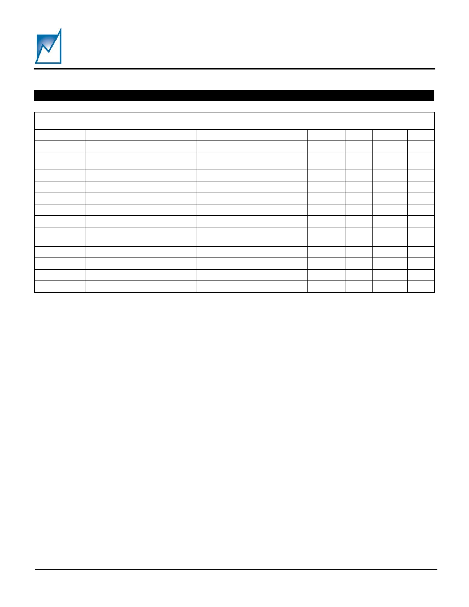
TABLE OF CONTENTS
General Description.................................
............3
Internal Functional Block Diagram...........
...............4
Pin Descriptions.......................................
........5-6
Package And Pin Configuration.....................
........7
Absolute Maximum Ratings.....................
.............8
Recommended Operating Conditions.........
.............8
DC Operating Characteristics.......................
.....8-10
AC Operating Characteristics........................
.......10
I
2
C 2-Wire Serial Interface AC Operating
Characteristics-100/400khz.....................
............11
Timing Diagrams...........................
...............11-12
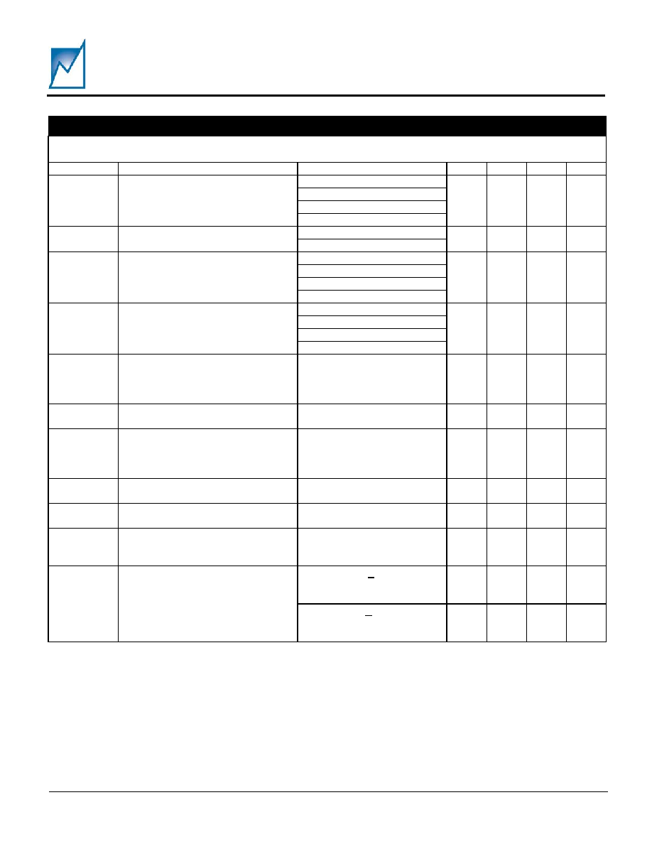
DEVICE OPERATION
Power
Supply........................................................
....14
Modes Of Operation....................................
.......14
Active DC Output Control...........................
....14-15
Power-On Cascade Sequencing................
...........15
Ongoing Operations-Monitoring Mode.........
...........16
Temperature Sensor Accuracy........................
.....16
Margining...................................................
.....17
Power-Off Cascade Sequencing...............
............17
Force-Shutdown...........................................
....17
Linked Operation............................................
...18
Restart.........................................................
...18
I
2
C Power-Off Control....................................
.....18
Recommended Use Of The Power On Pin.........
....19
Applications Schematic.................................
.....20
Development Hardware & Software............
...........21
I
2
C Programming Information
Serial Interface...........................................
.......22
Write.......................................................
........22
Read.......................................................
.......22
Write Protection............................................
....23
Configuration Registers...................................
...23
General-Purpose Memory...............................
....23
Command And Status Registers..................
.........23
ADC Conversions..........................................
....23
Graphical User Interface (GUI)...........................
..23
Write Protection Register Write........................
.....24
Configuration Register Read/Write...............
.....24-25
General-Purpose Memory Read/Write..............
.....26
Command And Status Register Read/Write......
......27
ADC Conversion Read...............................
........27
Default Configuration Register Settings..........
........28
Package.....................................................
.....29
Part Marking................................................
.....30
Ordering Information....................................
......30
Terminology And Definitions...........................
.....31
Legal Notice................................................
.....32
SMM764
Preliminary Information
Summit Microelectronics, Inc
2098 1.1 6/29/2005
3
The SMM764 is a highly integrated and accurate
power supply controller, monitor, and sequencer. Each
device has the ability to automatically control, monitor
and cascade sequence up to 4 power supplies. In
addition, the SMM764 includes Sequence-Link
a
feature that allows for the seamless integration of
other Sequence-Link devices to accommodate
sequencing of up to 46 channels. The SMM764 can
monitor the VDD input, the 12V input, two general-
purpose analog inputs, and the internal temperature
sensor. The SMM764 has four operating modes:
power-on sequencing modes, monitor mode, supply
margining mode using Active DC Output Control
(ADOC
TM
), and power-off sequencing mode.
Power-on sequencing is initiated by the rising edge of
the PWR_ON pin. During power-on sequencing the
SMM764 will sequence the power supply channels on,
in any order, by activating the PUP outputs and
monitoring the respective converter voltages to ensure
cascading of the supplies. Cascade sequencing is the
ability to hold off the next sequenced supply until the
first supply reaches a programmed threshold. A
programmable sequence termination timer can be set
to disable all channels if the power-on sequence stalls.
Once all supplies have sequenced on and the voltages
are above the UV settings, the ADOC, if enabled, will
bring the supply voltages to their nominal settings.
During this mode, the HEALTHY output will remain
inactive and the RST# output will remain active.
Once the power-on sequencing mode is complete, the
SMM764 enters monitor mode. In the monitor mode,
the SMM764 starts the ADOC control of the supplies
and adjusts the output voltage to the programmed
setting under all load conditions, especially useful for
supplies without sense lines. Typical converters have
±2% accuracy ratings for their output voltage; the
ADOC feature of the SMM764 increases the accuracy
to
±0.2% (using a ±0.1% external voltage
reference). The part also enables the triggering of
outputs by monitored fault conditions. The 10-bit ADC
cycles through all 9 channels every 2ms and checks
the conversions against the programmed threshold
limits. The results can be used to trigger RST#,
HEALTHY and FAULT# outputs as well as to initiate a
Fault-Triggered power-off or force-shutdown
operation.
While the SMM764 is in its monitoring mode, an I
2
C
command to margin the supply voltages can bring the
part into margining mode. In margining mode the
SMM764 can margin 4 supply voltages in any
combination of nominal, high and low voltage settings
using the ADOC feature, all to within ±0.2% using a
±0.1% external reference. The margin high and low
voltage settings can range from 0.3V to VDD around
the converters' nominal output voltage setting
depending on the specified margin range of the DC-
DC converter. During this mode the HEALTHY output
is always active and the RST# output is always
inactive regardless of the voltage threshold limit
settings and triggers. Furthermore, the triggers for
power-off and force-shutdown are temporarily
disabled.
The power-off sequencing mode can only be entered
while the SMM764 is in the monitoring mode. It can
be initiated by either bringing the PWR_ON pin low,
through I
2
C control, or triggered by a channel
exceeding its programmed thresholds. Once power-
off is initiated, it will disable the ADOC function and
sequence the PUP outputs off in the reverse order as
power-on sequencing. To ensure cascading of the
supplies during power-off sequencing all supplies will
be monitored as they turn off. The sequence
termination timer can be programmed to immediately
disable all channels if the power-off sequencing stalls
via a force-shutdown operation.
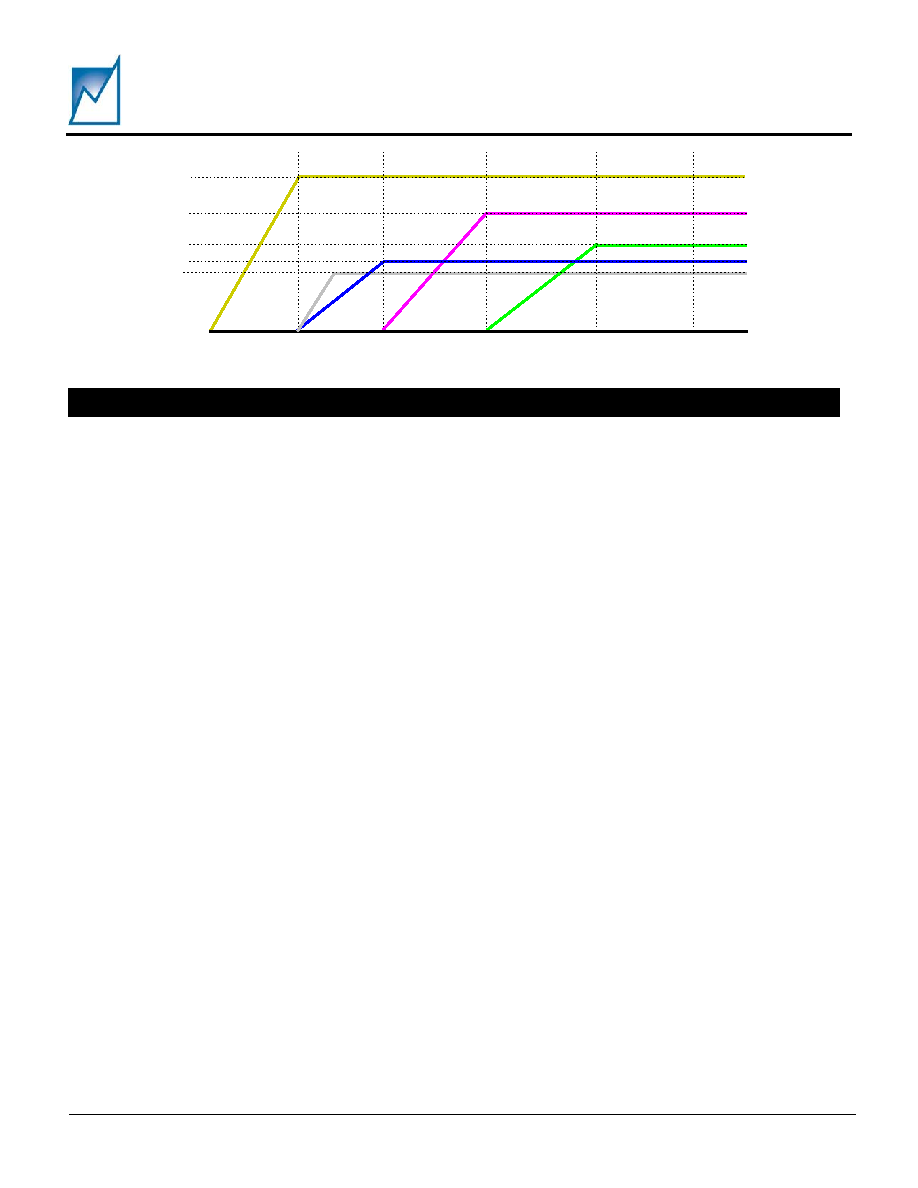
1
2.5V
1.8V
1.5V
VDD (+2.7V to +5.5V)
or 12VIN ( +8V to +15V)
2
3
4
SEQUENCE POSITION
1.2V
Figure 2 ≠ Example power supply sequencing and system start-up initialization using the SMM764. Cascade
sequencing ensures that all supplies in the previous sequence position are valid before the next channel is
released. Using the SMM764 any order of supply sequencing can be applied.
GENERAL DESCRIPTION
SMM764
Preliminary Information
Summit Microelectronics, Inc
2098 1.1 6/29/2005
4
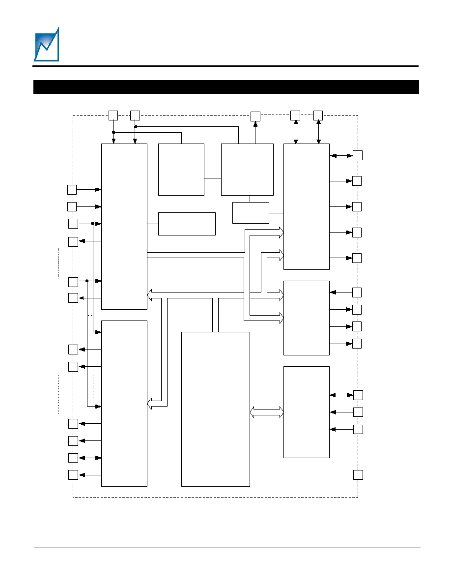
AIN
2
10-Bit ADC
AIN
1
VM
A
Active DC
Output
Control
(ADOC
TM
)
CAP
A
VM
D
CAP
D
TRIM
A
TRIM_CAP
A
TRIM
D
TRIM_CAP
D
VREF
FILT_CAP
12VIN
VDD
Cascade
Sequence
Control
FS#
PWR_ON
3.6V or
5.5V
Regulator
Power
Supply
Arbitrator
Temperature
Sensor
VDD_CAP
Output
Control
MR#
RST#
HEALTHY
FAULT#
Memory, Limit
and Status
Registers
I
2
C
Interface
SDA
SCL
A2
GND
UVLO
Control
PUP
A
SEQ_LINK
PUP
B
PUP
C
PUP
D
Figure 3 ≠ SMM764 Internal Functional Block Diagram.
INTERNAL FUNCTIONAL BLOCK DIAGRAM
SMM764
Preliminary Information
Summit Microelectronics, Inc
2098 1.1 6/29/2005
5
PIN DESCRIPTIONS
Pin
Number
Pin
Type
Pin Name
Pin Description
1
DATA SDA
SDA (Serial Data) is an open drain bi-directional pin used as the I
2
C data
line.
2
CLK SCL
SCL (Serial Clock) is an open drain input pin used as the I
2
C Clock line.
3
IN A2
The A2 (Address bit 2) pin is biased either to VDD_CAP or GND. When
communicating with the SMM764 over the 2-wire I
2
C bus, A2 provides a
mechanism for assigning a unique bus address.
4
IN MR#
MR# (Manual Reset) is an active low input. When asserted the RST# output
will become active. When de-asserted the RST# output will go inactive
immediately after a reset timeout period (t
RTO
) if there are no RST# trigger
sources active. This timeout period makes it suitable to use as a pushbutton
for manual reset purposes.
5
I/O PWR_ON
PWR_ON (Power On) is an open drain bi-directional pin. On the rising edge
of PWR_ON the part will sequence the supplies on, during the falling edge
the part will sequence the supplies off. This pin must be tied high through an
external pull-up resistor.
Note: The SMM764 does not monitor for faults during power-on/off
sequencing.
6
I/O FS#
FS# (Force Shutdown) is an open drain active low bi-directional pin. FS# is
used to immediately turn off all converter enable signals (PUP outputs) when
a fault is detected. Whenever FS# is asserted PWR_ON will automatically be
pulled low as well. This pin must be tied high through an external pull-up
resistor.
7
OUT FAULT#
The FAULT# pin is an active low open drain output. Active when a
programmed fault condition exists on AIN1, AIN2, or the internal temperature
sensor. When used, FAULT# should be pulled high through an external pull-
up resister.
8
OUT HEALTHY
HEALTHY is an active high open drain output. Active when all programmed
power supply inputs and monitored inputs are within OV and UV limits and
ADOC has begun. When used, HEALTHY should be pulled high through an
external pull-up resistor.
9
OUT RST#
RST# (Reset) is an active low open drain output pin. Active when a
programmed fault condition exists on any power supply inputs or monitored
inputs, when MR# is active, or when ADOC is not ready. RST# has a
programmable timeout period with options for 0.64ms, 25ms, 100ms and
200ms. When used, RST# should be pulled high through an external pull-up
resistor.
10
IN AIN1
AIN1 (Analog Input 1) is a general-purpose monitored analog input.
11
IN AIN2
AIN2 (Analog Input 2) is a general-purpose monitored analog input.
12,19,
24
GND GND
Ground.
SMM764
Preliminary Information
Summit Microelectronics, Inc
2098 1.1 6/29/2005
6
Pin
Number
Pin
Type
Pin Name
Pin Description
13
I/O SEQ_LINK
SEQ_LINK (Sequence-LinkTM) is an open drain bi-directional pin. This pin
should be attached to other Sequence-Link devices, during linked operation.
SEQ_LINK must be pulled high through an external pull-up resistor when
multiple Sequence-Link devices are used. When the SMM764 is not used
with another Sequence-Link device, SEQ_LINK should be tied directly to
ground.
14
I/O VREF
VREF (Voltage Reference) is a bi-directional analog pin. VREF is used for
Active DC Output Control and margining. VREF can be programmed to
output the internal 1.25V reference, or accept an external reference. VREF is
also used as a reference for the ADC.
15
CAP FILT_CAP
FILT_CAP (Filter Capacitor) is an external capacitor input used to filter VM
X
inputs.
16,17,
18,20,
21,22,
23,25
NC No
Connect Leave open, do not connect. These pins must be left floating.
41,36,
31,26
IN VM
X
VM
X
(Voltage Monitor) pins are analog inputs. These pins are normally
attached to the positive converter sense line, VM
A
through VM
D.
42,37,
32,27
CAP CAP
X
External capacitor input used to filter the VM
X
inputs to the 10-bit ADC, CAP
A
through CAP
D
. This provides an RC filter where R = 25k..
43,38,
33,28
OUT PUP
X
PUP
X
(Power Up Permitted) pins are programmable active high/low open
drain converter enable output, PUP
A
through PUP
D.
44,39,
34,29
OUT TRIM
X
Output voltage used to control the output of DC/DC converters, TRIM
A
through TRIM
D.
45,40,
35,30
CAP TRIM_CAP
X
TRIM_CAP
X
is an analog output pin used to control the output of DC/DC
converters. If the ADOC/margining functionality is not used on a channel the
associated TRIM_CAP
X
pin should be
left floating. There are 4 TRIM_CAP
X
pins, TRIM_CAP
A
through TRIM_CAP
D
.
46
PWR VDD
Power supply of the part
47
PWR 12VIN
12VIN (12 Volt Input) is a power supply input internally regulated to either
3.6V or 5.5V.
48
CAP VDD_CAP
VDD_CAP ( VDD Capacitor) is an external capacitor input used to filter the
internal supply.
PIN DESCRIPTIONS (Cont.)
SMM764
Preliminary Information
Summit Microelectronics, Inc
2098 1.1 6/29/2005
7
PACKAGE AND PIN CONFIGURATION
48 LEAD TQFP
TOP VIEW
48
47
46
45
44
43
42
41
40
39
38
37
36
35
34
33
32
31
30
29
28
27
26
25
1
2
3
4
5
6
7
8
9
10
11
12
13
14
15
16
17
18
19
20
21
22
23
24
SDA
SCL
A2
MR#
PWR_ON
FS#
FAULT#
HEALTHY
RST#
AIN1
AIN2
GND
SEQ
_L
INK
VRE
F
FILT_
CAP
NC
NC
NC
GND
NC
NC
NC
NC
GND
VMB
TRIM_CAPC
TRIMC
PUPC
CAPC
VMC
TRIM_CAPD
TRIMD
PUPD
CAPD
VMD
NC
VD
D_CAP
12
VIN
VD
D
TR
IM_CAPA
TR
IMA
PU
PA
CA
PA
VM
A
TR
IM_CAPB
TR
IMB
PU
PB
CA
PB
SMM764
Preliminary Information
Summit Microelectronics, Inc
2098 1.1 6/29/2005
8
Temperature Under Bias....................... -55
∞
C to 125
∞
C
Storage Temperature............................ -65
∞
C to 150
∞
C
Terminal Voltage with Respect to GND:
VDD Supply Voltage ......................... -0.3V to 6.0V
12VIN Supply Voltage ..................... -0.3V to 15.0V
PUP
A
, through PUP
F
....................... -0.3V to 15.0V
All Others ................................-0.3V to V
DD
+ 0.7V
Output Short Circuit Current ............................... 100mA
Lead Solder Temperature (10 s).......................... 300
∞
C
Junction Temperature .......................................... 150∞C
ESD Rating per JEDEC ....................................... 2000V
Latch-Up testing per JEDEC.............................
±
100mA
Note - The device is not guaranteed to function outside its operating rating.
Stresses listed under Absolute Maximum Ratings may cause permanent
damage to the device. These are stress ratings only and functional operation
of the device at these or any other conditions outside those listed in the
operational sections of the specification is not implied. Exposure to any
absolute maximum rating for extended periods may affect device performance
and reliability. Devices are ESD sensitive. Handling precautions are
recommended.
Temperature Range (Industrial)...........≠40
∞
C to +85
∞
C
(Commercial) ..............0
∞
C to +70
∞
C
VDD Supply Voltage .................................. 2.7V to 5.5V
12VIN Supply Voltage
1
............................6.0V to 14.0V
VIN ............................................................ GND to VDD
VOUT ...................................................... GND to 14.0V
Package Thermal Resistance (
JA
)
48 Lead TQFP ................................................80
o
C/W
Moisture Classification Level 1 (MSL 1) per J-STD- 020
RELIABILITY CHARACTERISTICS
Data Retention .............................................. 100 Years
Endurance..............................................100,000 Cycles
DC OPERATING CHARACTERISTICS
(Over recommended operating conditions, unless otherwise noted. All voltages are relative to GND.)
Symbol Parameter
Notes Min
Typ
Max
Unit
VDD
Supply voltage
2.7
5.5
V
Internally regulated to 5.5V
10 14
V
12VIN Supply
voltage
Internally regulated to 3.6V
6 14
V
I
DD
Power supply current from VDD
All TRIM pins floating,
12VIN floating
3 5
mA
I
12VIN
Power supply current from 12VIN
All TRIM pins floating,
VDD floating
3 5
mA
TRIM characteristics
TRIM sourcing maximum
current
1.5
mA
I
TRIM
TRIM output current through
100
to 1.0V
TRIM sinking maximum
current
1.5
mA
V
TRIM
Margin and ADOC range
Depends on TRIM range
of DC-DC converter
VREF/4 VDD V
TRIM_CAP characteristics
I
TRIM
_
CAP
TRIM output current through 1uF
capacitor to ground
Max acceptable board and
cap leakage is 50 nA 2
100 nA
All other input and output characteristics
VDD = 2.7V
0.8 x
VDD_CAP
V
V
IH
Input high voltage (MR#, SDA,
SCL, PWR_ON, SEQ_LINK,
FS#)
3
VDD = 5.0V
0.7 x
VDD_CAP
V
VDD = 2.7V
0.2 x
VDD_CAP
V
V
IL
Input low voltage (MR#, SDA,
SCL, PWR_ON, SEQ_LINK,
FS#)
3
VDD = 5.0V
0.3 x
VDD_CAP
V
ABSOLUTE MAXIMUM RATINGS
ABSOLUTE MAXIMUM RATINGS
SMM764
Preliminary Information
Summit Microelectronics, Inc
2098 1.1 6/29/2005
9
DC OPERATING CHARACTERISTICS (CONTINUED)
(Over recommended operating conditions, unless otherwise noted. All voltages are relative to GND.)
Symbol Parameter
Notes
Min
Typ
Max
Unit
Internally regulated to 3.6V
0.8 x
VDD_CAP
V
V
IH
Input high voltage (MR#, SDA,
SCL, PWR_ON, SEQ_LINK,
FS#)
3
Internally regulated to 5.5V
0.7 x
VDD_CAP
V
Internally regulated to 3.6V
0.2 x
VDD_CAP
V
V
IL
Input low voltage (MR#, SDA,
SCL, PWR_ON, SEQ_LINK,
FS#)
3
Internally regulated to 5.5V
0.3 x
VDD_CAP
V
V
OL
Open drain outputs (RST#,
FS#, PWR_ON, HEALTHY,
FAULT#, PUPx, SEQ_LINK)
I
SINK
= 1mA
0
0.4
V
I
OL
Output
low
current
Note ≠ Total I
SINK
from all PUPx pins
should not exceed 3mA or ADOC
ACC
specification will be affected
0 1.0
mA
V
SENSE
Positive sense voltage
VM pin
+0.3
VDD_CAP
V
V
MONITOR
Monitor threshold step size
VM, AIN1/AIN2 pins
5
mV
Commercial temp range
-3 +3
o
C
t
SA
Internal temperature sensor
accuracy
Industrial temp range
-5 +5
o
C
t
MONITOR
Temperature threshold step
size
Internal temp sensor
0.25
o
C
VREF
Internal 1.25 VREF output
voltage
1.24
1.25
1.26
V
≠40
∞
C to +85
∞
C
-0.25 +0.25 %
TC
Internal VREF temperature
coefficient
0
∞
C to +70
∞
C
-0.15 +0.15 %
VREF ACC Internal VREF accuracy
-0.4
+0.4
%
Ext VREF
External VREF voltage range
0.5
VDD_CAP
V
External VREF=1.25V,
±0.1%, total PUPx I
SINK
<
3ma, V
SENSE
<
3.5V
-0.2 0.1 +0.2 %
External VREF=1.25V,
±0.1%, total PUPx I
SINK
<
3ma, V
SENSE
>
3.5V
-0.5 0.3 +0.5 %
ADOC
ACC
ADOC (Active DC Output
Control)/margin accuracy
Internal VREF=1.25V, total
PUPx I
SINK
< 3ma
-0.5 0.3 +0.5 %
V
OUT_VALID
Minimum output valid voltage
VDD_CAP voltage at which
the PUP, RST#, HEALTHY
and FAULT#, FS#, PWR_ON
SEQ_LINK, outputs are valid
1 V
VDD_CAP rising
2.6
V
UVLO
UVLO (Under Voltage Lockout)
threshold
4
VDD_CAP falling
2.5
V
Note 1 ≠ Range depends on internal regulator set to 3.6V or 5.5V see 12VIN specification.
Note 2 ≠ See Application Note 37 which describes the type of capacitors to use to obtain minimum leakage.
Note 3 ≠ All logic levels are derived with respect to the voltage present on VDD_CAP, when supplied from the VDD input VDD_CAP is equal to
VDD, under no load.
Note 4 ≠ (100mV typ Hysteresis)
SMM764
Preliminary Information
Summit Microelectronics, Inc
2098 1.1 6/29/2005
10
DC OPERATING CHARACTERISTICS (CONTINUED)
(Over recommended operating conditions, unless otherwise noted. All voltages are relative to GND.)
AIN1/AIN2 ADC characteristics
Symbol Parameter
Notes
Min Typ
Max
Unit
N Resolution
10
Bits
MC Missing
codes
Minimum resolution for which no
missing codes are guaranteed
10 Bits
S/N
Signal-to-noise Ratio
Conversion rate = 500Hz
72
dB
DNL Differential
non-linearity
-1/2
+1/2
LSB
INL
Integral non-linearity
Note 1
-1
+1
LSB
GAIN
Positive full scale gain error
Note 1
-0.5
+0.5
%
OFFSET
Offset error
Note 1
-1
+1
LSB
ADC_TC
Full scale temperature
coefficient
±15
PPM/
o
C
IM
ADC
Analog ADC Input Impedance
10
M
II
VREF
VREF input current
250
nA
IC
VREF
VREF input capacitance
200
pF
IR
VREF
VREF input impedance
1
k
Note 1 - The formula for the total ADC inaccuracy is: [((ADC read voltage) +/- INL)*(range of gain error)]+range of offset error
SMM764
Preliminary Information
Summit Microelectronics, Inc
2098 1.1 6/29/2005
11
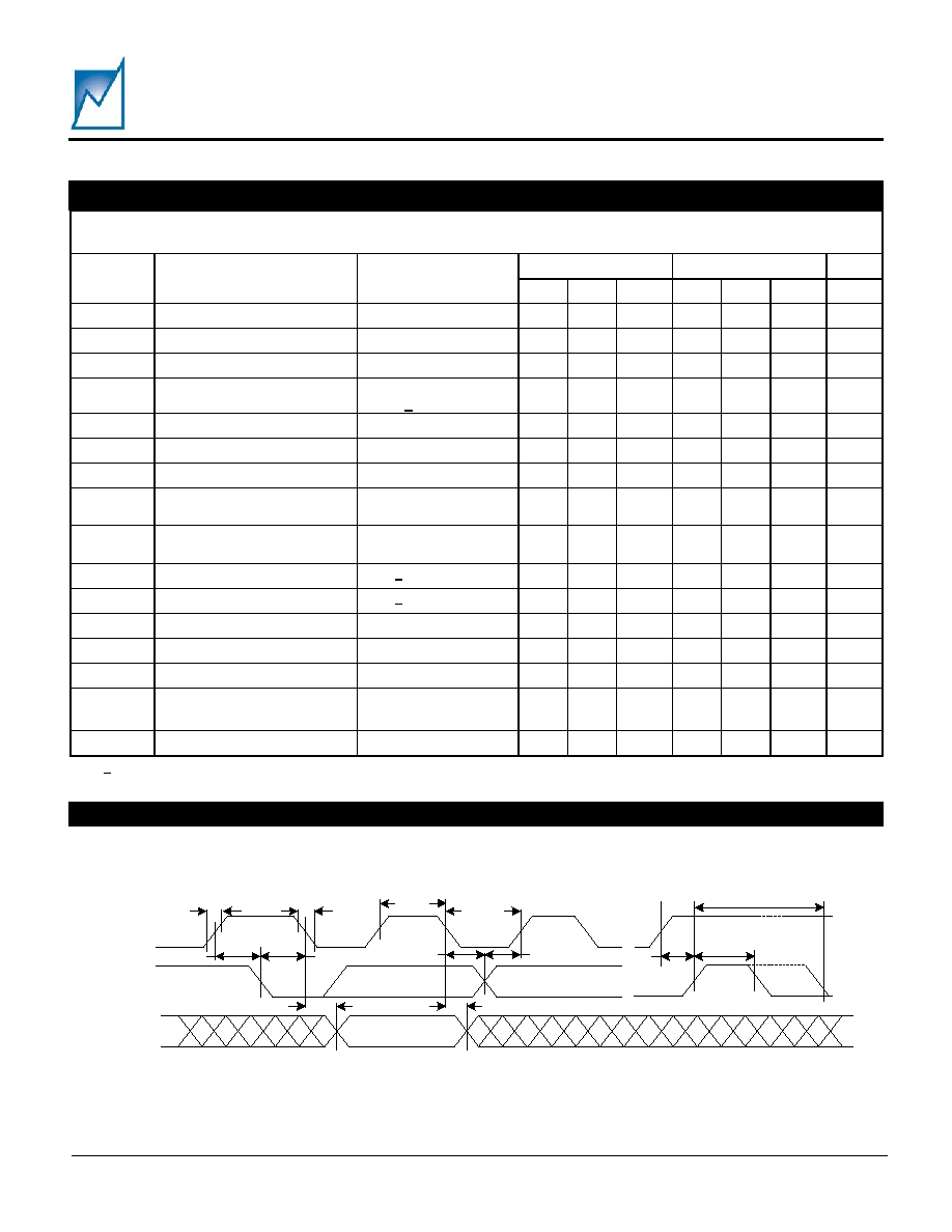
Over recommended operating conditions, unless otherwise noted. All voltages are relative to GND. See Figure 5
and 6 Timing diagrams.
Symbol Description
Conditions
Min
Typ
Max
Unit
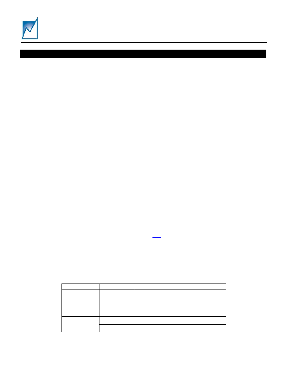
t
DPON
= 0.64ms
t
DPON
= 12.5ms
t
DPON
= 25ms
t
DPON
Programmable power-on delay
from restart timer expiration to
PUP
X
active.
t
DPON
= 50ms
-25 t
DPON
+25 %
t
DPOFF
= 0.64ms
t
DPOFF
Programmable power-off delay
from VM
X
off to PUP
X
inactive
t
DPOFF
= 12.5ms
-25 t
DPOFF
+25 %
t
PRTO
= 0.64ms
t
PRTO
= 25ms
t
PRTO
= 100ms
t
PRTO
Programmable reset time-out delay
t
PRTO
= 200ms
-25 t
PRTO
+25 %
t
STT
= OFF
t
STT
= 100ms
t
STT
= 200ms
t
STT
Programmable sequence
termination timer
t
STT
= 400ms
-25 t
STT
+25 %
t
FTRD
Fault-triggered restart delay
Time from restart timer
expiration to PUP
X
active
after a fault-triggered power-
off or force-shutdown.
2.4 s
t
FTRD
ACC
Fault-triggered restart delay
accuracy
-25 t
FTRD
+25 %
t
CTRD
Command-triggered restart delay
Time from restart timer
expiration to PUP
X
active
after command-triggered
power-off or force-shutdown.
12.5 ms
t
CTRD
ACC
Command-triggered restart delay
accuracy
-25 t
CTRD
+25 %
T
ADC
10-bit ADC sampling period
Time for ADC conversion of
all 9 channels
2.0 ms
T
DC_CONTROL
ADOC sampling period
Update period for ADOC of
channels
A ≠ D
1.7 ms
Slow Margin, + 10% change
in voltage with 0.1% ripple
TRIM_CAP=1
µF
850 ms
t
MARGIN
Margin Time from Nominal
Fast Margin, + 10% change
in voltage with 0.1% ripple
TRIM_CAP=1
µF
85 ms
AC OPERATING CHARICTERISTICS
SMM764
Preliminary Information
Summit Microelectronics, Inc
2098 1.1 6/29/2005
12
I
2
C-2 WIRE SERIAL INTERFACE AC OPERATING CHARACTERISTICS ≠100/400 kHz
Over recommended operating conditions, unless otherwise noted. All voltages are relative to GND.
See Figure 4 Timing Diagram.
100kHz 400kHz
Symbol Description
Conditions
Min Typ Max Min Typ Max Units
f
SCL
SCL clock frequency
0
100
0
400
KHz
T
LOW
Clock low period
4.7
1.3
µs
T
HIGH
Clock high period
4.0
0.6
µs
t
BUF
Bus free time
Before new transmission
-
Note 1/
4.7 1.3 µs
t
SU:STA
Start condition setup time
4.7
0.6
µs
t
HD:STA
Start condition hold time
4.0
0.6
µs
t
SU:STO
Stop condition setup time
4.7
0.6
µs
t
AA
Clock edge to data valid
SCL low to valid
SDA (cycle n)
0.2 3.5 0.2 0.9 µs
t
DH
Data output hold time
SCL low (cycle n+1)
to SDA change
0.2 0.2 µs
t
R
SCL and SDA rise time
Note 1/
1000
1000
ns
t
F
SCL and SDA fall time
Note 1/
300 300 ns
t
SU:DAT
Data in setup time
250
150
ns
t
HD:DAT
Data in hold time
0
0
ns
TI
Noise filter SCL and SDA
Noise suppression
100
100
ns
t
WR_CONFIG
Write cycle time config
Configuration
registers
10 10
ms
t
WR_EE
Write cycle time EE
Memory array
5 5 ms
Note: 1/ - Guaranteed by Design.
t
R
t
F
t
HIGH
t
LOW
t
SU:SDA
t
HD:SDA
t
SU:DAT
t
HD:DAT
t
SU:STO
t
BUF
t
DH
t
AA
SCL
SDA
(IN)
SDA
(OUT)
t
W R (For W rite Operation Only)
Figure 4 - Basic I
2
C Serial Interface Timing
TIMING DIAGRAMS
SMM764
Preliminary Information
Summit Microelectronics, Inc
2098 1.1 6/29/2005
13
Figure 5 - The SMM764 cascade sequencing the supplies on and then monitoring for fault conditions.
Figure 6 - The SMM764 cascade sequencing the supplies off.
TIMING DIAGRAMS (CONTINUED)
t
DPONA
t
DPONB
t
DPONC
t
DPOND
1
2
3
VM
A
PUP
A
PUP
B
PUP
C
PUP
D
VM
B
VM
C
VM
D
Sequence
Position
t
DPOFFA
t
DPOFFB
t
DPOFFC
t
DPOFFD
3
2
1
VM
A
PUP
A
PUP
B
PUP
C
PUP
D
VM
B
VM
C
VM
D
Sequence
Position
SMM764
Preliminary Information
Summit Microelectronics, Inc
2098 1.1 6/29/2005
14
APPLICATIONS INFORMATION
DEVICE OPERATION
POWER SUPPLY
The SMM764 can be powered by either a 12V input
through the 12VIN pin or by a 3.3V or 5.0V input
through the VDD pin. The 12VIN pin feeds an internal
programmable regulator that internally generates
either 5.5V or 3.6V. A voltage arbitration circuit allows
the device to be powered by the highest voltage from
either the regulator output or the VDD input. This
voltage arbitration circuit continuously checks for these
voltages to determine which will power the SMM764.
The resultant internal power supply rail is connected to
the VDD_CAP pin that allows both filtering and hold-
up of the internal power supply. To ensure that the
input voltage is high enough for reliable operation, an
under voltage lockout circuit holds the controlled
supplies off until the UVLO thresholds are met. When
multiple Sequence-LinkTM devices are connected, the
same VDD and/or 12VIN supplies must power all
devices.
MODES OF OPERATION
The SMM764 has four basic modes of operation
(shown in Figures 5 through 8): power-on sequencing
mode, ongoing operations-monitoring mode, supply
margining mode, and power-on sequencing mode. In
addition, there are two features:
ADOC and force-shutdown, which can be used during
monitoring and margining mode. A detailed description
of each mode and feature follows.
ACTIVE DC OUTPUT CONTROL (ADOC
TM
)
The SMM764 can actively control the DC output
voltage of bricks or DC/DC converters that have a trim
pin during monitoring and margining mode. The
converter may be an off-the shelf compact device, or
may be a "roll your own" circuit on the application
board. In either case, the SMM764 dramatically
improves voltage accuracy (down to 0.2%) by
implementing closed-loop ADOC active control. This
utilizes the DC-DC's "trim" pin as shown in Figure 12,
or an equivalent output voltage feedback adjustment
"VADJ", "FB", or "Sense" node in a user's custom
circuit, Figure 13. Each of the TRIM
X
pins on the
SMM764 is connected to the trim input pins on the
power supply converters. A sense line from the
channel's point-of-load connects to the corresponding
VM input. The ADOC function cycles through all 4
channels (A-D) every 1.7ms making slight adjustments
to the voltage on the associated TRIM
X
output pins
based on the voltage inputs on the VM
X
pins. These
voltage adjustments allow the SMM764 to control the
output voltage of power supply converters to within
±0.2% when using a ±0.1% external voltage reference.
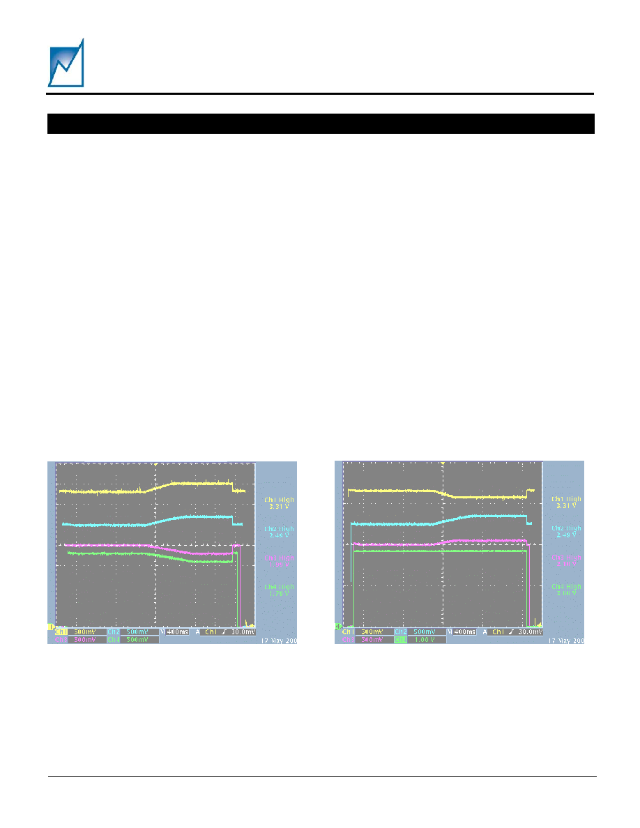
Figure 7 - Waveform shows four SMM764 channels
exhibiting Sequence-on to Nominal voltage, Margin
High or Low, Nominal voltage and then sequence-off
Ch 1 = 3.3V DC-DC converter output (Yellow trace)
Ch 2 = 2.5V DC-DC converter output (Blue trace)
Ch 3 = 2.0V DC-DC converter output (Purple trace)
Ch 4 = 1.8V DC-DC converter output (Green trace)
Figure 8 - Waveform shows three SMM764 channels
Sequencing-on to Nominal voltage, Margin High and
Low, and then sequence-off. Channel 4 shows the
HEALTHY signal.
Ch 1 = 3.3V DC-DC converter output (Yellow trace)
Ch 2 = 2.5V DC-DC converter output (Blue trace)
Ch 2 = 2.0V DC-DC converter output (Purple trace)
Ch 4 = Healthy signal output (Green trace)

SMM764
Preliminary Information
Summit Microelectronics, Inc
2098 1.1 6/29/2005
15
A pulse of current either sourced or sunk for 5µs every
1.7ms, to the capacitors connected to the TRIM_CAP
X
pins adjusts the voltage output on the TRIM
X
pins.
The voltages on the TRIM_CAP
X
pins are buffered
and applied to the TRIM
X
pins. The voltage
adjustments on the TRIM
X
pins cause a slight ripple of
less than 1mV on the power supply voltages. The
amplitude of this ripple is a function of the TRIM_CAP
X
capacitor and the trim gain of the converter.
Application Note 37 details the calculation of the
TRIM_CAP
X
capacitor to achieve a desired minimum
ripple.
Each channel can be programmed to either enable or
disable the ADOC function. When disabled or not
active, the TRIM
X
pins on the SMM764 are high
impedance inputs. If disabled and not used, they can
be connected to ground. The voltages on the TRIM
X
pins are buffered and applied to the TRIM_CAP
X
pins
charging the capacitors. This allows a smooth
transition from the converter powering up to its
nominal voltage, to the SMM764 controlling that
voltage, and to the ADOC nominal setting.
The pulse of current can be increased to a 10X pulse
of current until the power supply voltages are at their
nominal settings by selecting the programmable Fast
Margin option. As the name implies, this option
decreases the time required to bring a supply voltage
from the converter's nominal output voltage to the
ADOC nominal, high, or low voltage setting.
POWER-ON CASCADE SEQUENCING
The SMM764 can be programmed to sequence on 32
supplies occupying up to 29 sequence positions. This
is accomplished using the SEQ_LINK pin. Each of the
4 channels (A-D) on a SMM764 has an associated
open drain PUP output that, when connected to a
converter's enable pin, controls the turn-on of the
converter. The channels are assigned sequence
positions to determine the order of the sequence. The
polarity of each of the PUP
X
outputs is programmable
for use with various types of converters.
Power-on sequencing is initiated on the rising edge of
the PWR_ON pin.
The SMM764 can be programmed to wait until any or
all VDD, 12VIN, and Internal Temp (Internal
Temperature) ADC readings are within their respective
voltage threshold or temperature limits before power-
on sequencing is allowed to begin. This ensures that
the converters have reached their full supply voltage
before they are enabled.
On the rising edge of the PWR_ON pin the SMM764
will wait a power-on delay time (t
DPON
) for any
channels in the first sequence position (position 1) and
then activate the PUP
X
outputs for those channels.
The power-on delay times are individually
programmable for each channel. The SMM764 will
then wait until all VM
X
inputs of the channels assigned
to the first sequence position are above their user
programmable UV1 thresholds, which is called
cascade sequencing.
At this point, the SMM764 will enter the second
sequence position (position 2) and begin to timeout
the power-on delay times for the associated channels.
This process continues until all of the channels
assigned to participate in the sequence have turned
on and are above their UV1 threshold. Once the
sequence has completed the status register indicates
that all sequenced power supply channels have turned
on. After the sequence has completed the SMM764
will begin the ADOC of the enabled channels. The
power-on sequencing mode ends when the ADOC
channels are at their nominal voltage setting. The
"Ready" bit in the status register signifies that the
voltages are at their set points.
The programmable sequence termination timer can be
used to protect against a stalled power-on sequence.
This timer resets itself at the beginning of each
sequence position. All channels in the sequence
position must go above their UV1 threshold before the
sequence termination timer times out (t
STT
) or the
sequence will terminate by pulling the FS# pin low,
initiating a Force Shutdown. The status register
contains bits indicating in which sequence position the
timer timed out. This sequence termination timer has
four settings of OFF, 100ms, 200ms and 400ms.
While the SMM764 is in the power-on sequencing
mode the RST# output is held active and the
HEALTHY output is held inactive regardless of trigger
sources (Figure 8). The power-off and force-shutdown
trigger options are also disabled while in this mode.
Furthermore, the SMM764 will not respond to activity
on the PWR_ON pin or to a power-off I
2
C command
during power-on sequencing mode.
The SMM764 permits multiple supplies to occupy the
same sequence position. When a sequence position is
shared, each channel will be enabled after its
respective power-on delay. When the last channel
occupying a shared sequence position exceeds its
UV1 setting the SMM764 will increment to the next
APPLICATIONS INFORMATION (CONTINUED)

SMM764
Preliminary Information
Summit Microelectronics, Inc
2098 1.1 6/29/2005
16
sequence position. Any unused channel should be
assigned to the null sequence position.
ONGOING OPERATIONS-MONITORING MODE
During ongoing operations mode, the part can monitor,
and actively control via ADOC, and use the force-
shutdown operation if necessary.
Once the power-on sequence is complete, depending
on the user programmed settings; the SMM764 will
either enter the ongoing operations mode directly or
wait for ADOC to successfully bring all channels within
their nominal values. The ongoing operations mode
will end when a power-off sequence, or force-
shutdown has been initiated.
Once the ongoing operations mode has begun, the
SMM764 continues to monitor all VM
X
inputs, the VDD
and 12VIN inputs, and two temperature sensor inputs
with a 10-bit ADC. Each of these inputs is sampled
and converted by the ADC every 2ms. The ADC input
has a range of 0V to four times the voltage on VREF
for inputs VM
A-D
and the VDD input. The range is
extended to 12 times VREF for the 12VIN input and is
reduced to two times VREF for the AIN1 and AIN2
inputs.
The SMM764 monitors internal temperature using the
10-bit ADC and the automonitor function. Two under-
temperature and two over-temperature thresholds can
be set, each with its own programmable threshold
options and consecutive conversion, before trigger
counter. Resolution is 0.25 C per bit scaled over the
range of -128 C to 127.75 C. The temperature value
can be acquired over the I
2
C bus as a 10-bit signed
two's complement value.
The SMM764 compares each resulting ADC
conversion with two programmable 10-bit under-
voltage limits (UV1, UV2) and two programmable 10-
bit over-voltage limits (OV1, OV2) for the
corresponding input. A consecutive conversion
counter is used to provide filtering of the ADC inputs.
Each limit can be programmed to require 1, 2, 4 or 6
consecutive out-of-limit conversions before it is said to
be in fault. One in-limit conversion will remove the
fault from the threshold limit. This provides digital
filtering of the monitored inputs. The ADC inputs VM
A-D
can use additional filtering by connecting a capacitor
from the corresponding CAP
X
pins to ground to form
an analog RC filter (R=25k
). The input is considered
to be in a fault condition if any of its limit thresholds
are in fault. Setting an OV threshold limit to full-scale
(3FF
HEX
), or setting a UV threshold limit to 000
HEX
,
ensures that the limit can never be in fault. The status
registers provide the real-time status of all monitored
inputs.
The voltage threshold limits for inputs VM
A-D
, VDD and
12VIN can be programmed to trigger the RST# and
HEALTHY outputs as well as a Fault-Triggered force-
shutdown and power-off operation when exceeded.
The threshold limits for the internal temperature
sensor and the AIN1 and AIN2 inputs can be
programmed to assert the RST#, HEALTHY, and
FAULT# output pins
The HEALTHY and FAULT# outputs of the SMM764
are active as long as the monitored threshold remains
in violation. The RST# output also remains active as
long as the monitored threshold remains in violation.
However, once the threshold violation goes away, the
RST# will remain active for a programmable reset
timeout period (t
PRTO
).
The SMM764 treats Command-Triggered force-
shutdown and power-off operations, those
caused by
I
2
C commands and assertion of the FS# and
PWR_ON pin, differently than those caused by a
Fault-Triggered forced-shutdown and power-off
conditions, those caused by UV/OV violations or a
sequence termination timer expiration. The mode in
which either a forced-shutdown or a power-off occurs
effects how or whether the SMM764 will restart, and
the number of allowable retries permitted.
TEMPERATURE SENSOR ACCURACY
The internal temperature sensor accuracy is ±5
o
C from
-40 to +85
o
C. The sensor measures the temperature
of the SMM764 die and the ambient temperature. If
VDD is at 5V, the die temperature is +2
o
C and at 12V,
it is +4
o
C. In order to calculate this difference in
specific applications, measure the VDD or 12VIN
supply current and calculate the power dissipated and
multiply by 80
o
C/W. For instance, 5V and 5mA is
25mW, which creates a 2
o
C offset.
MARGINING
The SMM764 has two additional ADOC voltage
settings for channels A-D, margin high and margin
low. The margin high and margin low voltage settings
can range from 0.3V to VDD of the converters'
nominal output voltage, depending on the specified
margin range of the DC-DC converter. These
settings are stored in the configuration registers and
are loaded into the ADOC voltage setting by margin
commands issued via the I
2
C bus. The channel must
be enabled for ADOC in order to enable margining.
The margin command registers contain two bits for
APPLICATIONS INFORMATION (CONTINUED)

SMM764
Preliminary Information
Summit Microelectronics, Inc
2098 1.1 6/29/2005
17
APPLICATIONS INFORMATION (CONTINUED)
each channel that decode the commands to margin
high, margin low, or control to the nominal setting.
Therefore, any combination of margin high, margin
low, and nominal control is allowed in the margining
mode.
Once the SMM764 receives the command to margin
the supply voltages, it begins adjusting the supply
voltages to move toward the desired setting. When all
channels are at their voltage setting, a bit is set in the
margin status registers.
Note: Configuration writes or reads of registers 00
HEX
to 0F
HEX
should not be performed while the SMM764 is
margining.
POWER-OFF CASCADE SEQUENCING
The SMM764 performs power-off sequencing in the
reverse order of power-on sequencing.
Power-off cascade sequencing can be initiated by the
PWR_ON pin, via I
2
C control or triggered by a fault
condition on any of the monitored inputs. Toggling the
PWR_ON pin low will initiate the power-off sequence.
To enable software control of the power-off
sequencing feature, the SMM764 offers an I
2
C
command to initiate power-off sequencing while the
PWR_ON pin is asserted. Furthermore, power-off
sequencing can be initiated by a fault condition on a
monitored input.
Once power-off sequencing begins, the SMM764 will
wait a power-off delay time (t
DPOFF
) for any channel in
the last sequence position and then deactivate the
PUP outputs for those channels. The power-off delay
times are individually programmable for each channel.
The
SMM764
will
then
wait
until
all
VM
X
inputs of the channels assigned to that sequence
position are below the programmed OFF thresholds.
At this point, the SMM764 will move to the next
sequence position and begin to timeout the power-off
delay times for the associated channels. This process
continues until all of the channels in the sequence
have turned off and are below their OFF thresholds.
The status register reveals that all sequenced
channels have turned off. The power-off sequencing
mode ends when all sequenced supplies are below
their OFF thresholds.
The programmable sequence termination timer can be
used to protect against a stalled power-off sequence.
This timer resets itself at the beginning of each
sequence position. All channels in the sequence
position must go below their OFF threshold before the
sequence termination timer times out (t
STT
) or the
sequence will terminate and all PUP outputs will be
switched to their inactive state. This timer has four
settings of OFF: 100ms, 200ms and 400ms. The
sequence termination timer can be disabled separately
for power-off sequencing.
While the SMM764 is in the power-off sequencing
mode, the RST# output is held active and the
HEALTHY output is held inactive, regardless of trigger
sources (Figure 8). The force-shutdown trigger option
is also disabled while in this mode. Furthermore, the
SMM764 will not respond to activity on the PWR_ON
pin during power-off sequencing mode.
FORCE SHUTDOWN
The force-shutdown operation brings all PUP
X
outputs
to their inactive state. This operation is used for an
emergency shutdown when there is not enough time
to sequence the supplies off. The force-shutdown
operation shuts off all sequenced channels pulls the
PWR_ON pin low, and waits for the supply voltages to
drop below their respective OFF thresholds before
beginning a restart sequence.
A force-shutdown operation can be initiated by any
one of four events. The first two methods for initiating
a force-shutdown are always enabled. Simply taking
the FS# pin low will initiate a force-shutdown operation
and maintain it until the pin is brought high again. An
I
2
C force-shutdown command allows the force-
shutdown operation to be initiated via software control.
This bit is cleared after all sequenced channels have
dropped below their OFF voltage threshold.

SMM764
Preliminary Information
Summit Microelectronics, Inc
2098 1.1 6/29/2005
18
APPLICATIONS INFORMATION (CONTINUED)
LINKED OPERATION
The SMM764 can be linked to multiple Sequence-
Link
devices to create a seamless multi-channel
power manager. With linked operation 8 Sequence-
Link devices in a system can sequence up to 46
supplies within 29 sequence positions. The
sequencing in this mode can be interlaced, sequencing
a supply from device A, then from device B, then again
from device A, etc. This extended sequencing is made
possible by the inclusion of a SEQ_LINK pin.
For this mode of operation, the control pins, including
SEQ_LINK, PWR_ON, and FS# on each device must
be tied together. In addition, the VDD and 12V supply
must also be connected on all linked devices. As a
consequence when multiple devices are linked
together, all devices must be powered by the same
supply.
RESTART
There are two possible conditions in which a restart
sequence may be initiated. The first instance occurs
when either the FS# pin is asserted or the PWR_ON
pin is pulled low thus initiating a command-triggered
restart. The second condition occurs when a user
programmable fault triggers a force-shutdown
operation or a power-off sequence thus resulting in a
fault-triggered restart.
In either case, the SMM764 will wait until all voltages
have fallen below their user programmable OFF
thresholds, after all channels are off, the PWR_ON pin
will continue to be held low for a period of time
dependent on the nature of the fault.
When a power-off or force-shutdown condition results
from a command-triggered power-off or force-
shutdown, the SMM764 will automatically begin the
restart procedure. When restart begins an internal
timer will begin to timeout for a command-triggered
Restart Delay (t
CTRD
) of 12.5 ms. After this time has
expired the PWR_ON pin is released, allowing the
power-on sequence to begin.
When a power-off or force-shutdown condition results
from a fault-triggered power-off or force-shutdown, the
SMM764 may or may not begin the restart procedure
(see PROGRAMMABLE RETRIES), if restart begins
the internal timer will begin to timeout a fault-triggered
Restart Delay (t
FTRD
) of 2.4 s before the PWR_ON pin
is released allowing the power-on Sequence to begin.
If the SMM764 is programmed to wait for VDD, 12VIN,
or Internal Temp to be valid (above UV1 and below
OV1) before power-on sequencing may commence,
then this condition will be checked after the restart
timer has expired and the PWR_ON pin has been
released.
The conditions that may lead to a Fault-Triggered
restart include any channel exceeding its user
programmable thresholds (OV or UV), set to trigger
either a force-shutdown or a power-off sequence. In
addition, in the event that the sequence termination
timer times out before a channel reaches its UV1 or
OFF threshold, during sequencing, a Fault-Triggered
restart occur.
I
2
C POWER OFF CONTROL
Power-on sequencing is only permitted while the
PWR_ON pin is active. Once the PWR_ON pin is
active and the SMM764 has entered monitoring mode,
an I
2
C command may be issued to commence the
power-off sequence. This condition will continue until
an I
2
C "power on" command is issued.
PROGRAMMABLE RETRIES
In the event of a persistent system fault, the SMM764
may be programmed to limit the number of Fault-
Triggered restarts it will allow. This programmable
setting ensures that the SMM764 will not enter a
hiccup-mode of operation, while still reducing
susceptibility to transient fault conditions.
In the event of a Fault-Triggered restart the fault will
be registered and internally compared to the maximum
number of allowable faults. If this number is exceeded
then the fault condition will be latched and the
PWR_ON and FS# pins will be pulled low while the
RST# output is asserted. This fault condition will
remain latched until power is cycled on the SMM764,
at which point the PWR_ON and FS# pins will be
released, the number of faults will be reset zero, and
the restart sequence will begin. The allowable
programmable setting include one, three, and
unlimited retries.
SMM764
Preliminary Information
Summit Microelectronics, Inc
2098 1.1 6/29/2005
19
APPLICATIONS INFORMATION (CONTINUED)
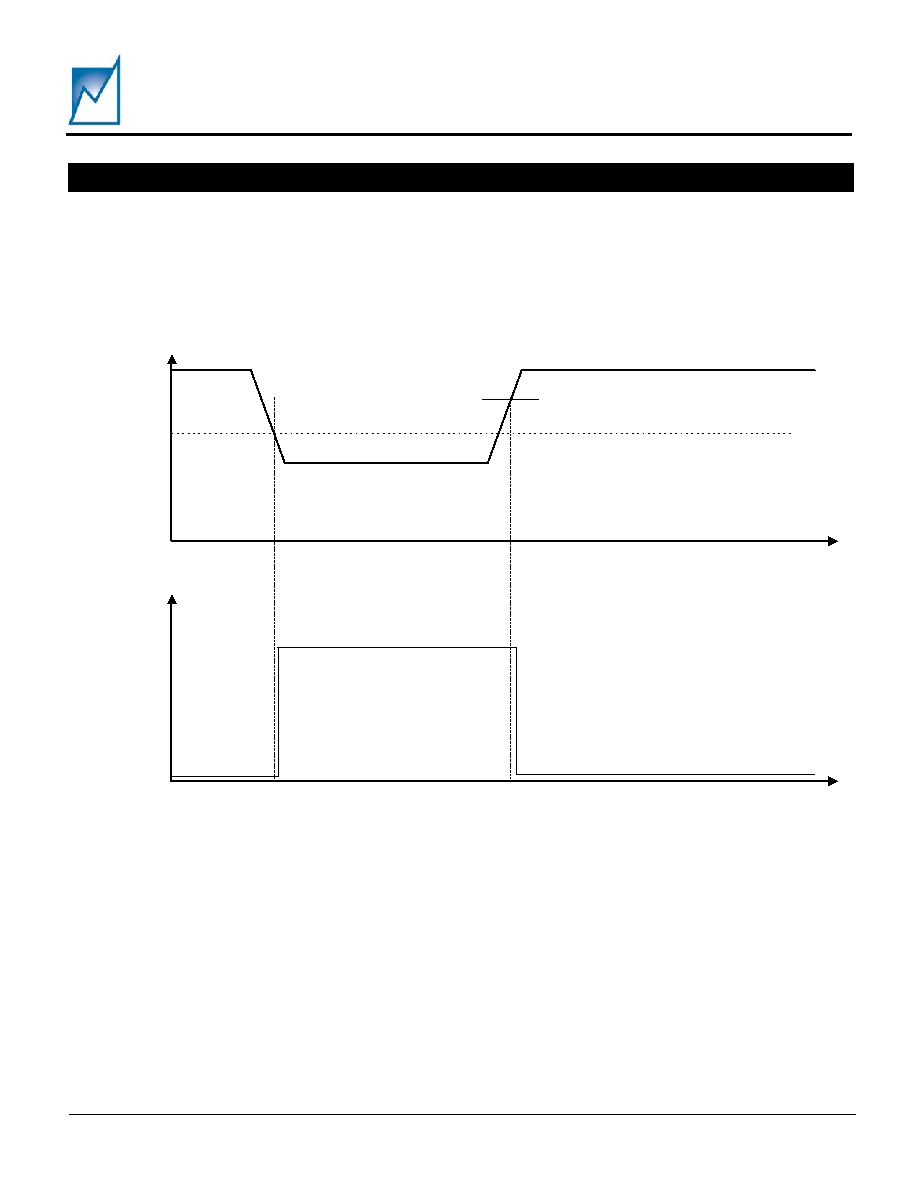
UNDERVOLTAGE LOCKOUT
The internally filtered supply voltage as seen across
VDD_CAP is edge-triggered to lock out false or
nuisance signals during both the power-on and power-
off sequences. If the VDD_CAP voltage falls below
2.5V (Figure 10), an internal undervoltage lockout
(UVLO) circuit will reset all internal logic. Once power
has recovered above 2.6V the SMM764 will restart as
if a Command-Triggered power-off had been issued.
VDD_CAP
2.5V
3.6V, 5.5V
UVLO
(Internal)
2.6V
Figure 10 - Timing Sequence recovering from a VDD_CAP Power `Brown-Out'
SMM764
Preliminary Information
Summit Microelectronics, Inc
2098 1.1 6/29/2005
20
VDD_
CAP
1
1
2
2
3
3
J1 3 Jum
per
3.3VO
U
T
2.5VO
U
T
TO
ADDI
TI
ONAL
CONVERTERS
SW
1
SW
PUSHBUTTO
N
FAULT#
HEALTHY
RESET#
C6
8
0.
01uF
+12VIN
Place Trim
Caps as close to
device as possible
+5VIN
MR
#
VDD_
CAP
C4
1
0.
01uF
1
2
D1
5
DIODE
C
4
3
0
.
01uF
Place Trim
Caps as close to
device as possible
C
4
4
0
.
1uF
VDD
C
4
5
0
.
022uF
1
1
2
2
3
3
J2 3 Jum
per
Re
f
1
Gnd
2
EN
3
VIn
4
VO
u
t
5
U1
0
LM
4121
+
V
out
1
+
V
out
2
S
ense
3
+
V
out
4
Gnd
5
Gnd
6
+V
i
n
7
+V
i
n
8
PW
R EN
9
Tr
im
10
E
nabl
e
11
U1
3
T
Y
C
O
A
X
H
010A
0F
C1
2
0.
01uF
C1
3
0.
1uF
0
C1
4
0.
01uF
C1
5
0.
1uF
C4
2
0.
01uF
SDA
R8
10K
R9
10K
VDD
D1
4
Healthy
R1
0
10K
D3
RST
D4
Fault
1
1
2
2
3
3
J3
3 Jum
per
+
V
out
1
+
V
out
2
S
ense
3
+
V
out
4
Gnd
5
Gnd
6
+V
i
n
7
+V
i
n
8
PW
R EN
9
Tr
im
10
E
nabl
e
11
U1
4
T
Y
C
O
A
X
H
010A
0F
C1
6
0.
01uF
C1
7
0.
1uF
C1
8
0.
01uF
C2
4
1uF
C1
9
0.
1uF
C2
5
0.
01uF
SW
2
SW
PUSHBUTTO
N
1
1
2
2
3
3
J4
3 Jum
per
+
V
out
1
+
V
out
2
S
ense
3
+
V
out
4
Gnd
5
Gnd
6
+V
i
n
7
+V
i
n
8
PW
R EN
9
Tr
im
10
E
nabl
e
11
U1
5
T
Y
C
O
A
X
H
010A
0F
C2
0
0.
01uF
C2
1
0.
1uF
C1 0.
1uF
C2
2
0.
01uF
C2
3
0.
1uF
SDA
1
SCL
2
A2
3
MR
#
4
PW
R_
O
N
/O
FF
5
FS#
6
F
aul
t
#
7
H
eal
t
h
y
8
RST
#
9
AIn
1
10
AIn
2
11
GND
12
SEQ
_
L
I
NK
13
VREF
14
FILT_CAP
15
VM
D
26
CAPD
27
PUPD
28
TR
IM
D
29
TRIM
_
C
APD
30
VM
C
31
CAPC
32
PUPC
33
TR
IM
C
34
TRIM
_
C
APC
35
VM
B
36
CAPB
37
PUPB
38
TR
IM
B
39
TRIM
_
C
APB
40
VM
A
41
CAPA
42
PUPA
43
TR
IM
A
44
TRIM
_
C
APA
45
VDD
46
12VIN
47
VDD_CAP
48
GND
19
GND
24
U1
SMM764
C4
6
0.
1uF
C3
2
0.
1uF
C3
3
0.
01uF
C3
4
0.
01uF
C3
5
0.
01uF
C3
6
0.
1uF
+
C3
7
10uF
C3
8
0.
1uF
VDD
1
2
R1
1
47K
1
2
R1
2
47K
1
2
R1
3
47K
1
2
R1
6
47K
t
RT
1
10K
R1
4
30K
Gnd
1
SCL
2
Gnd3
3
SDA
4
Rsrv5
5
MR
6
+10V
7
Rsrv8
8
+5V
9
Rsrv10
10
J7
I2
C
R1
5
30K
C6
7
0.
01uF
t
RT
2
10K
VDD
C6
6
0.
01uF
J5
VREF
A2
+
V
out
1
+
V
out
2
S
ense
3
+
V
out
4
Gnd
5
Gnd
6
+V
i
n
7
+V
i
n
8
PW
R EN
9
Tr
im
10
E
nabl
e
11
U1
2
T
Y
C
O
A
X
H
010A
0F
C3
9
0.
01uF
1
2
R1
47K
SCL
1.5VO
U
T
1.2VO
U
T
1
2
R2
47K
C2
0.
01uF
C3
0.
01uF
C4
0.
01uF
C5 0.
1uF
C6
0.
01uF
C4
7
0.
01uF
C4
8
0.
1uF
C4
9
0.
022uF
+
C7 10uF
Re
f
1
Gnd
2
EN
3
VIn
4
VO
u
t
5
U1
1
LM
4121
1
1
2
2
3
3
J6
VREF_
I
N
PW
R_O
N
C8 0.
1uF
C5
0
0.
1uF
1
2
R3
47K
J8 VREF
1
1
2
2
3
3
J9
VREF_
I
N
VDD_
CAP
VDD
1
2
R4
47K
SDA
1
SCL
2
A2
3
MR
#
4
PW
R_
O
N
/O
FF
5
FS#
6
F
aul
t
#
7
H
eal
t
h
y
8
RST
#
9
AIn
1
10
AIn
2
11
GND
12
SEQ
_
L
I
NK
13
VREF
14
FILT_CAP
15
VM
D
26
CAPD
27
PUPD
28
TR
IM
D
29
TRIM
_
C
APD
30
VM
C
31
CAPC
32
PUPC
33
TR
IM
C
34
TRIM
_
C
APC
35
VM
B
36
CAPB
37
PUPB
38
TR
IM
B
39
TRIM
_
C
APB
40
VM
A
41
CAPA
42
PUPA
43
TR
IM
A
44
TRIM
_
C
APA
45
VDD
46
12VIN
47
VDD_CAP
48
GND
19
GND
24
U2
SMM764
C9
0.
1uF
C2
6
1uF
C2
7
.
01uF
S
M
X
3200
Program
m
e
r
Connector
FS#
C2
8
1uF
C2
9
.
01uF
FAULT#
HEALTHY
O
p
tional External
Tem
p
erature
Sensors
LINK
VDD
R1
7
10K
R1
8
10K
RESET#
A2
MR
#
R5
10K
R6
10K
VDD
D1
3
Healthy
R7
10K
D2
RST#
D1
Fault#
C1
0
0.
01uF
VDD
C1
1
0.
1uF
C4
0
0.
01uF
R1
9
10K
VDD
R2
1
10K
R2
0
10K
VDD_
CAP
C3
0
1uF
C3
1
0.
01uF
Input Voltage Option
E
i
ther +5V
or +12V
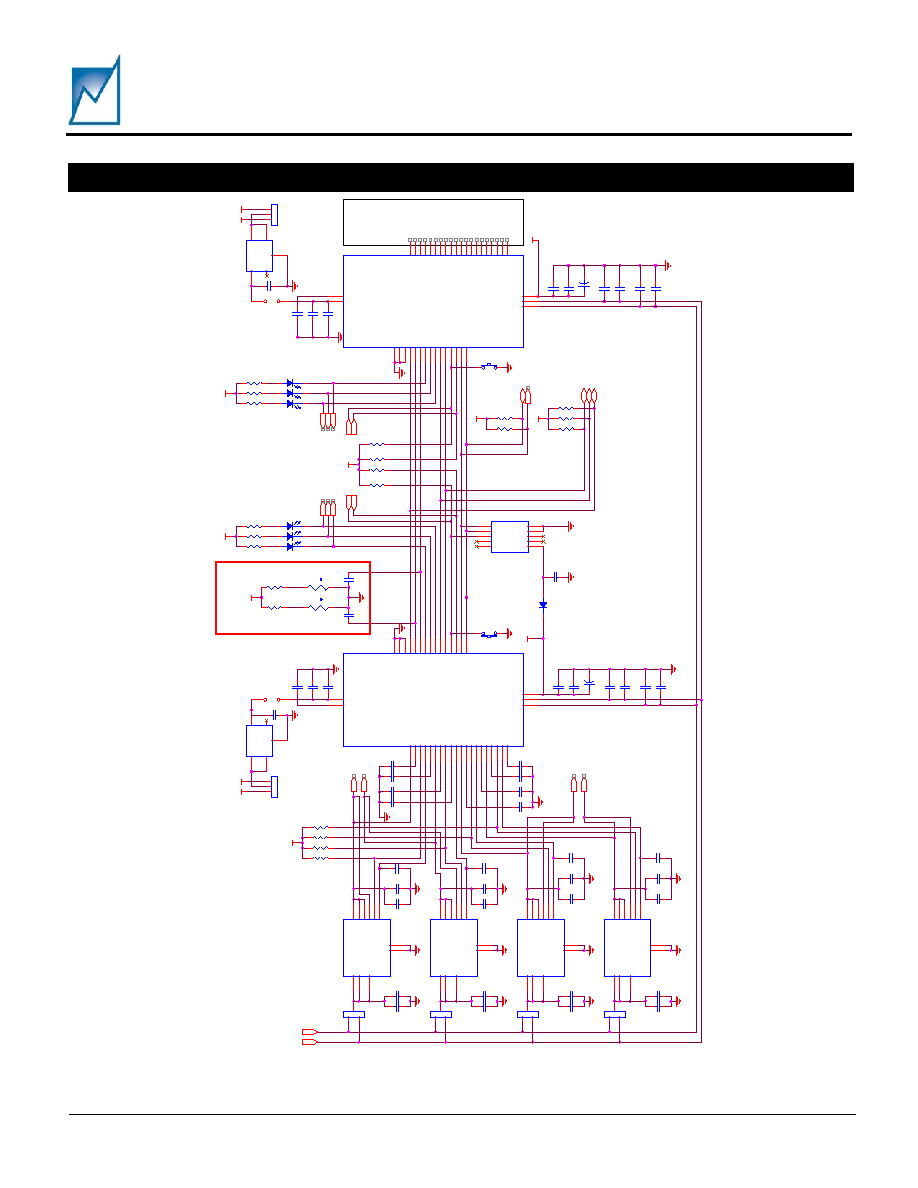
Figure 11 ≠ SMM764 Distributed power applications schematic. The accuracy of the external reference
(U10) sets the accuracy of the ADOC function. Total accuracy with a ±0.1% external reference is ±0.2%
APPLICATIONS INFORMATION (CONTINUED)
SMM764
Preliminary Information
Summit Microelectronics, Inc
2098 1.1 6/29/2005
21
DEVELOPMENT HARDWARE & SOFTWARE
The end user can obtain the Summit SMX3200
programming system for device prototype
development. The SMX3200 system consists of a
programming Dongle, cable and Windows
TM
GUI
software. It can be ordered on the website or from a
local representative.
The SMX3200 programming Dongle/cable interfaces
directly between a PC's parallel port and the target
application. The device is then configured on-screen
via an intuitive graphical user interface employing
drop-down menus.
The Windows GUI software will generate the data and
send it in I
2
C serial bus format so that it can be directly
downloaded to the SMM764 via the programming
Dongle and cable. An example of the connection
interface is shown in Figure 15.
When design prototyping is complete, the software
can generate a HEX data file that should be
transmitted to Summit for approval. Summit will then
assign a unique customer ID to the HEX code and
program production devices before the final electrical
test operations. This will ensure proper device
operation in the end application.
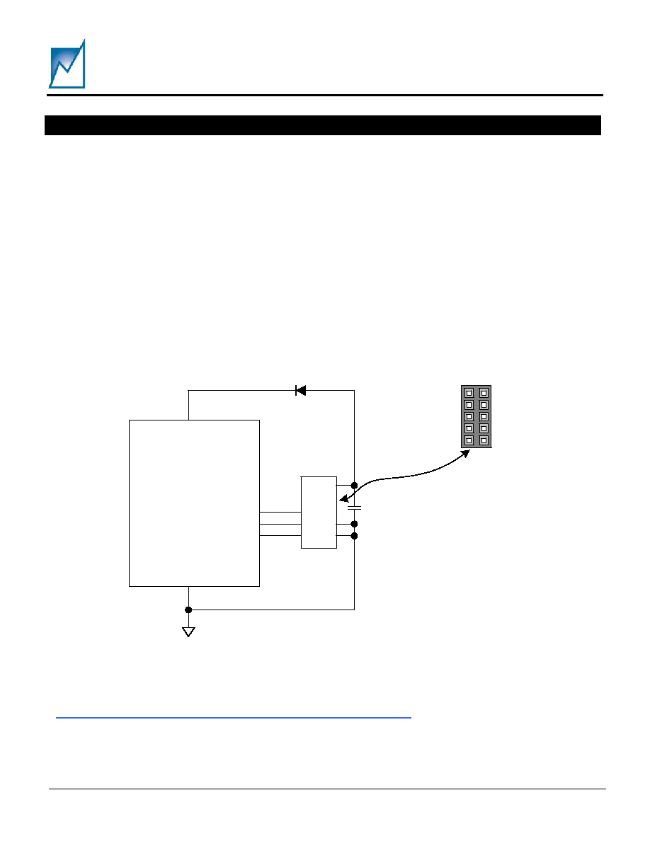
Pin 9, 5V
Pin 7, 10V
Pin 5, Reserved
Pin 3, GND
Pin 1, GND
Pin 6, MR#
Pin 4, SDA
Pin 2, SCL
Pin 8, Reserved
Pin 10, Reserved
Top view of straight 0.1" x 0.1 closed-side
connector. SMX3200 interface cable connector.
9
7
5
3
1
10
8
6
4
2
SMM764
SDA
SCL
VDD_CAP
GND
0.1
µF
MR#
D1
1N4148
Figure 12 ≠ SMX3200 Programmer I
2
C serial bus connections to program the SMM764. Note that the MR#
pin does not need to be connected to pin 6 for programming purposes.
The latest revisions of all software and an application brief describing the SMX3200 is available from the website at:
http://www.summitmicro.com/tech_support/program_kit/SMX3200.htm

SMM764
Preliminary Information
Summit Microelectronics, Inc
2098 1.1 6/29/2005
22
SERIAL INTERFACE
Access to the configuration registers, general-purpose
memory and command and status registers is carried
out over an industry standard 2-wire serial interface
(I
2
C). SDA is a bi-directional data line and SCL is a
clock input. Data is clocked in on the rising edge of
SCL and clocked out on the falling edge of SCL. All
data transfers begin with the MSB. During data
transfers SDA must remain stable while SCL is high.
Data is transferred in 8-bit packets with an intervening
clock period in which an Acknowledge is provided by
the device receiving data. The SCL high period (t
HIGH
)
is used for generating Start and Stop conditions that
precede and end most transactions on the serial bus.
A high-to-low transition of SDA while SCL is high is
considered a Start condition while a low-to-high
transition of SDA while SCL is high is considered a
Stop condition.
The interface protocol allows operation of multiple
devices and types of devices on a single bus through
unique device addressing. The address byte is
comprised of a 4-bit device type identifier SA[3:0]
(slave address) and a 3-bit bus address BA[2:0]. The
remaining bit indicates either a read or a write
operation. Refer to Table 1 for a description of the
address bytes used by the SMM764.
The device type identifier for the memory array is
generally set to 1010
BIN
following the industry standard
for a typical nonvolatile memory. There is an option to
change the identifier to 1011
BIN
allowing it to be used
on a bus that may be occupied by other memory
devices. The configuration registers are grouped with
the memory array and thus use 1010
BIN
or 1011
BIN
as
the device type identifier. The command and status
registers as well as the 10-bit ADC are accessible with
the separate device type identifier of 1001
BIN
.
The bus address bits BA[1:0] are programmed into the
configuration registers. Bus address bit BA[2] can be
programmed as either 0 or biased by the A2 pin. The
bus address accessed in the address byte of the serial
data stream must match the setting in the SMM764
and on the A2 pin.
Any access to the SMM764 on the I
2
C bus will
temporarily halt the monitoring function. This does not
affect the ADOC function, which will continue
functioning and control the DC outputs. This is true
not only during the monitor mode, but also during
power-on and power-off sequencing when the device
is monitoring the channels to determine if they have
turned on or turned off.
The SMM764 halts the monitor function from when it
acknowledges the address byte until a valid stop is
received.
WRITE
Writing to the memory or a configuration register is
illustrated in Figures 13, 14, 15, 17 and 19. A Start
condition followed by the address byte is provided by
the host; the SMM764 responds with an Acknowledge;
the host then responds by sending the memory
address pointer or configuration register address
pointer; the SMM764 responds with an acknowledge;
the host then clocks in on byte of data. For memory
and configuration register writes, up to 15 additional
bytes of data can be clocked in by the host to write to
consecutive addresses within the same page. After
the last byte is clocked in and the host receives an
Acknowledge, a Stop condition must be issued to
initiate the nonvolatile write operation.
READ
The address pointer for the configuration registers,
memory, command and status registers and ADC
registers must be set before data can be read from the
SMM764. This is accomplished by a issuing a dummy
write command, which is simply a write command that
is not followed by a Stop condition. The dummy write
command sets the address from which data is read.
After the dummy write command is issued, a Start
command followed by the address byte is sent from
the host. The host then waits for an Acknowledge and
then begins clocking data out of the slave device. The
first byte read is data from the address pointer set
during the dummy write command. Additional bytes
can be clocked out of consecutive addresses with the
host providing an Acknowledge after each byte. After
the data is read from the desired registers, the read
operation is terminated by the host holding SDA high
during the Acknowledge clock cycle and then issuing a
Stop condition. Refer to Figures 16, 18 and 21 for an
illustration of the read sequence.
I
2
C PROGRAMMING INFORMATION
SMM764
Preliminary Information
Summit Microelectronics, Inc
2098 1.1 6/29/2005
23
WRITE PROTECTION
The SMM764 powers up into a write protected mode.
Writing a code to the volatile write protection register
can disable the write protection. The write protection
register is located at address 87
HEX
of slave address
1001
BIN
.
Writing 0101
BIN
to bits [7:4] of the write protection
register allow writes to the general-purpose memory
while writing 0101
BIN
to bits [3:0] allow writes to the
configuration registers. The write protection can re-
enable by writing other codes (not 0101
BIN
) to the write
protection register. Writing to the write protection
register is shown in Figure 13.
CONFIGURATION REGISTERS
The majority of the configuration registers are grouped
with the general-purpose memory located at either
slave address 1010
BIN
or 1011
BIN
. Bus address bits
BA[2:1] are programmable. The bus address bit BA[0],
however, is used to differentiate the general-purpose
memory from the configuration registers and should be
set to 1
BIN
when accessing the configuration registers
.
Bus address bit BA[2] can be programmed as a
"virtual 0" or biased by the A2 pin.
An additional configuration register is located at
address 84
HEX
of slave address 1001
BIN
.
Writing and reading the configuration registers is
shown in Figures 14, 15, 16, 17, and 18
Note: Configuration writes or reads of registers 00
HEX
to 0F
HEX
should not be performed while the SMM764 is
margining.
GENERAL-PURPOSE MEMORY
The 2k-bit general-purpose memory is located at
either slave address 1010
BIN
or 1011
BIN
. Bus address
bits BA[2:1] are programmable. The bus address bit
BA[0], however, is used to differentiate the general-
purpose memory from the configuration registers and
should be set to 0
BIN
when accessing general purpose
memory
.
Bus address bit BA[2] can be programmed
as a "virtual 0" or biased by the A2 pin.
The slave address and bus address must be set each
time the memory is accessed. Memory writes and
reads are shown in Figures 19, 20 and 21.
COMMAND AND STATUS REGISTERS
The command and status registers are located at
slave address 1001
BIN
. Writes and reads of the
command and status registers are shown in Figures
22 and 23.
ADC CONVERSIONS
An ADC conversion on any monitored channel can be
performed and read over the I
2
C bus using the ADC
read command. The ADC read command, shown in
Figure 24, starts with a dummy write to the 1001
BIN
slave address. Bits [6:3] of the word address byte are
used to address the desired monitored input. Once
the device acknowledges the channel address, it
begins the ADC conversion of the addressed input.
This conversion requires 70
µs to complete. During
this conversion time, acknowledge polling can be
used. The SMM764 will not acknowledge the address
bytes until the conversion is complete. When the
conversion has completed, the SMM764 will
acknowledge the address byte and return the 10-bit
conversion along with a 4-bit channel address echo.
GRAPHICAL USER INTERFACE (GUI)
Device configuration utilizing the Windows based
SMM764 graphical user interface (GUI) is highly
recommended. The software is available from the
Summit website (website at:
(
http://www.summitmicro.com/tech_support/tech.htm#
GUI
.
Using the GUI in conjunction with this datasheet
simplifies the process of device prototyping and the
interaction of the various functional blocks. A
programming Dongle (SMX3200) is available from
Summit to communicate with the SMM764. The
Dongle connects directly to the parallel port of a PC
and programs the device through a cable using the I
2
C
bus protocol.
Slave Address Bus Address Register Type
1001
BIN
BA2 BA1 BA0
Write Protection Register,
Command and Status Registers,
One Configuration Registers,
ADC Conversion Readout
BA2 BA1 0
2-k Bits of General-Purpose Memory
1010
BIN
or
1011
BIN
BA2 BA1 1
Configuration Registers
Table 1 - Address bytes used by the SMM764.
I
2
C PROGRAMMING INFORMATION (CONTINUED)
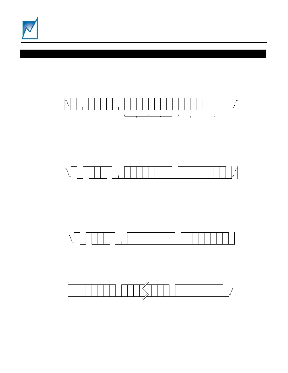
SMM764
Preliminary Information
Summit Microelectronics, Inc
2098 1.1 6/29/2005
24
S
T
A
R
T
W
A
C
K
Master
Slave
A
C
K
Configuration
Register Address = 87
HEX
1
0
0
0
0
1
1
1
0
1
0
1
0
1
0
1
S
T
O
P
Data = 55
HEX
A
C
K
1
0
0
1
B
A
2
Bus Address
B
A
1
B
A
0
5
HEX
Unlocks
General Purpose
EE
5
HEX
Unlocks
Configuration
Registers
Write Protection
Register Address
8
HEX
7
HEX
Figure 13 ≠ Write Protection Register Write
S
T
A
R
T
1
B
A
2
Bus Address
W
A
C
K
Master
Slave
A
C
K
1
B
A
1
0
1
S
A
0
Configuration
Register Address
C
7
C
6
C
5
C
4
C
3
C
2
C
1
C
0
D
7
D
6
D
5
D
4
D
3
D
2
D
1
D
0
S
T
O
P
Data
A
C
K
Figure14 ≠ Configuration Register Byte Write
D
7
D
6
D
5
D
4
D
3
D
2
D
1
D
0
S
T
O
P
Master
Slave
Data (16)
A
C
K
D
7
D
6
D
5
D
4
D
3
D
2
D
1
D
0
Data (2)
A
C
K
D
7
D
6
D
5
D
2
D
1
D
0
A
C
K
S
T
A
R
T
1
Bus Address
W
A
C
K
Master
Slave
A
C
K
1
B
A
1
0
1
S
A
0
Configuration
Register Address
C
7
C
6
C
5
C
4
C
3
C
2
C
1
C
0
D
7
D
6
D
5
D
4
D
3
D
2
D
1
D
0
Data
A
C
K
B
A
1
Figure 15 ≠ Configuration Register Page Write
I
2
C PROGRAMMING INFORMATION (CONTINUED)
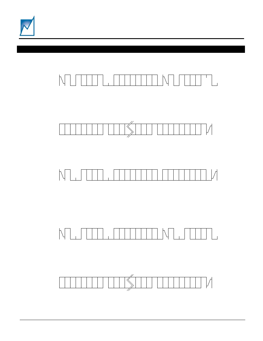
SMM764
Preliminary Information
Summit Microelectronics, Inc
2098 1.1 6/29/2005
25
S
T
A
R
T
1
B
A
2
Bus Address
W
A
C
K
D
7
D
6
D
5
D
4
D
3
D
2
D
1
D
0
S
T
O
P
N
A
C
K
Master
Master
Slave
Slave
A
C
K
Data (n)
1
B
A
1
0
1
S
A
0
Configuration
Register Address
C
7
C
6
C
5
C
4
C
3
C
2
C
1
C
0
S
T
A
R
T
1
R
A
C
K
B
A
2
Bus Address
1
S
A
0
0
1
A
C
K
D
7
D
6
D
5
D
2
D
1
D
0
A
C
K
D
7
D
6
D
5
D
4
D
3
D
2
D
1
D
0
Data (1)
B
A
1
Figure 16 - Configuration Register Read
S
T
A
R
T
W
A
C
K
Master
Slave
A
C
K
Configuration
Register Address
C
7
C
6
C
5
C
4
C
3
C
2
C
1
C
0
D
7
D
6
D
5
D
4
D
3
D
2
D
1
D
0
S
T
O
P
Data
A
C
K
1
0
0
1
B
A
2
Bus Address
B
A
1
B
A
0
Figure 17 - Configuration Register with Slave Address 1001
BIN
Write
S
T
A
R
T
W
A
C
K
D
7
D
6
D
5
D
4
D
3
D
2
D
1
D
0
S
T
O
P
N
A
C
K
Master
Master
Slave
Slave
A
C
K
Data (n)
Configuration
Register Address
C
7
C
6
C
5
C
4
C
3
C
2
C
1
C
0
S
T
A
R
T
R
A
C
K
A
C
K
D
7
D
6
D
5
D
2
D
1
D
0
A
C
K
D
7
D
6
D
5
D
4
D
3
D
2
D
1
D
0
Data (1)
1
0
0
1
B
A
2
Bus Address
B
A
1
B
A
0
1
0
0
1
B
A
2
Bus Address
B
A
1
B
A
0
Figure 18 - Configuration Register with Slave Address 1001
BIN
Read
I
2
C PROGRAMMING INFORMATION (CONTINUED)
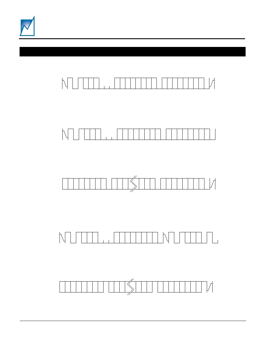
SMM764
Preliminary Information
Summit Microelectronics, Inc
2098 1.1 6/29/2005
26
S
T
A
R
T
1
Bus Address
W
A
C
K
Master
Slave
A
C
K
0
1
S
A
0
Configuration
Register Address
C
7
C
6
C
5
C
4
C
3
C
2
C
1
C
0
D
7
D
6
D
5
D
4
D
3
D
2
D
1
D
0
S
T
O
P
Data
A
C
K
B
A
2
0
B
A
1
Figure 19 ≠ General Purpose Memory Byte Write
Bus Address
B
A
2
0
S
T
A
R
T
1
W
A
C
K
D
7
D
6
D
5
D
4
D
3
D
2
D
1
D
0
S
T
O
P
Master
Master
Slave
Slave
A
C
K
Data (16)
0
1
S
A
0
Configuration
Register Address
C
7
C
6
C
5
C
4
C
3
C
2
C
1
C
0
A
C
K
D
7
D
6
D
5
D
4
D
3
D
2
D
1
D
0
Data (1)
A
C
K
D
7
D
6
D
5
D
4
D
3
D
2
D
1
D
0
Data (2)
A
C
K
D
7
D
6
D
5
D
2
D
1
D
0
A
C
K
B
A
1
Figure 20 - General Purpose Memory Page Write
S
T
A
R
T
1
W
A
C
K
D
7
D
6
D
5
D
4
D
3
D
2
D
1
D
0
S
T
O
P
N
A
C
K
Master
Master
Slave
Slave
A
C
K
Data (n)
0
1
S
A
0
Configuration
Register Address
C
7
C
6
C
5
C
4
C
3
C
2
C
1
C
0
S
T
A
R
T
1
R
A
C
K
1
S
A
0
0
A
C
K
D
7
D
6
D
5
D
2
D
1
D
0
A
C
K
D
7
D
6
D
5
D
4
D
3
D
2
D
1
D
0
Data (1)
Bus Address
B
A
2
0
Bus Address
B
A
1
B
A
2
0
B
A
1
Figure 21 - General Purpose Memory Read
I
2
C PROGRAMMING INFORMATION (CONTINUED)
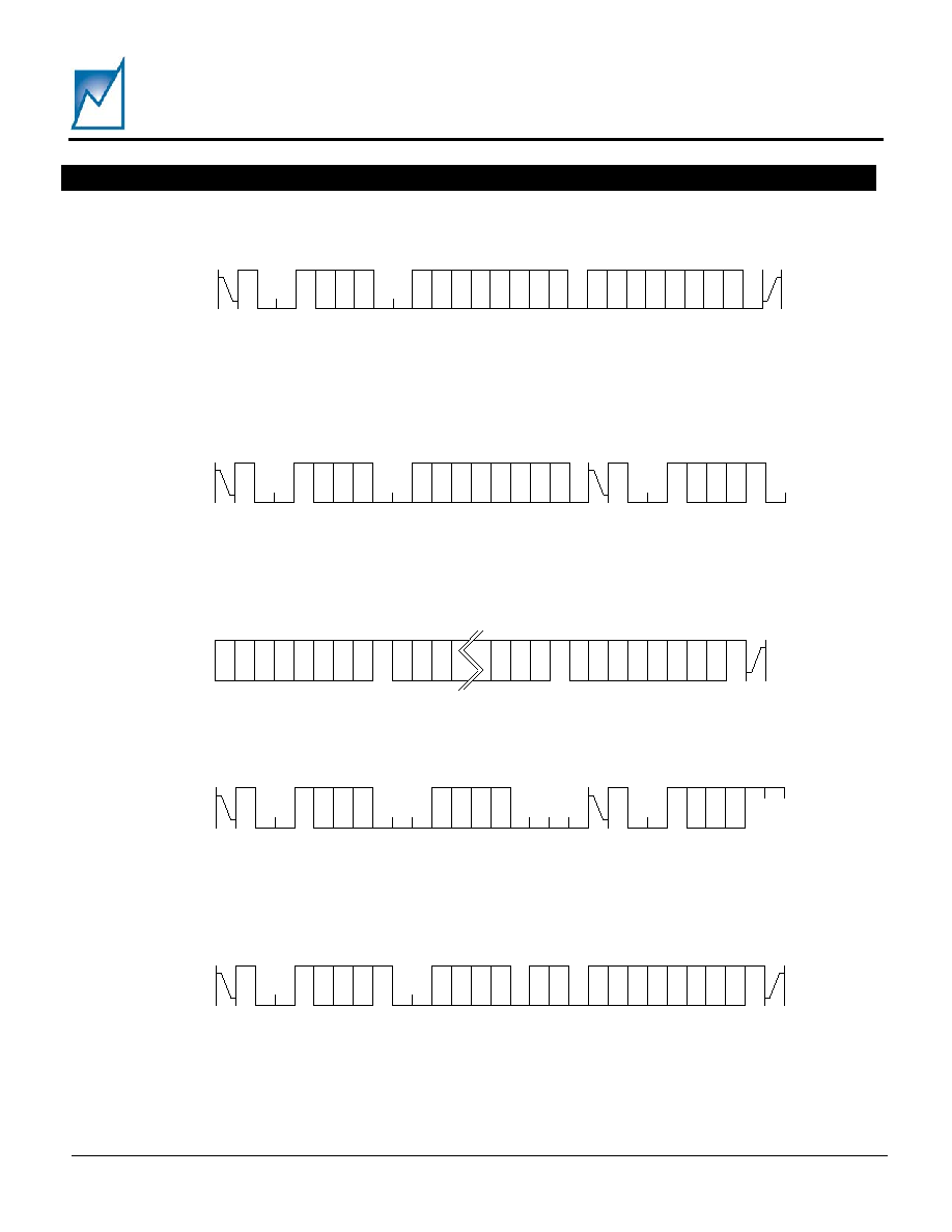
SMM764
Preliminary Information
Summit Microelectronics, Inc
2098 1.1 6/29/2005
27
S
T
A
R
T
W
A
C
K
Master
Slave
A
C
K
Command and Status
Register Address
C
7
C
6
C
5
C
4
C
3
C
2
C
1
C
0
D
7
D
6
D
5
D
4
D
3
D
2
D
1
D
0
S
T
O
P
Data
A
C
K
1
0
0
1
B
A
2
Bus Address
B
A
1
B
A
0
Figure 22 ≠ Command and Status Register Write
S
T
A
R
T
W
A
C
K
D
7
D
6
D
5
D
4
D
3
D
2
D
1
D
0
S
T
O
P
N
A
C
K
Master
Master
Slave
Slave
A
C
K
Data (n)
Command and Status
Register Address
C
7
C
6
C
5
C
4
C
3
C
2
C
1
C
0
S
T
A
R
T
R
A
C
K
A
C
K
D
7
D
6
D
5
D
2
D
1
D
0
A
C
K
D
7
D
6
D
5
D
4
D
3
D
2
D
1
D
0
Data (1)
1
0
0
1
B
A
2
Bus Address
B
A
1
B
A
0
1
0
0
1
B
A
2
Bus Address
B
A
1
B
A
0
Figure 23 - Command and Status Register Read
S
T
A
R
T
1
0
0
1
B
A
2
Bus Address
B
A
1
B
A
0
W
C
H
3
C
H
2
C
H
1
C
H
0
A
C
K
S
T
A
R
T
1
0
0
1
B
A
2
Bus Address
B
A
1
B
A
0
R
S
T
A
R
T
1
0
0
1
B
A
2
Bus Address
B
A
1
B
A
0
R
C
H
3
C
H
2
C
H
1
C
H
0
D
9
D
8
D
7
D
6
D
5
D
4
D
3
D
2
D
1
D
0
S
T
O
P
N
A
C
K
N
A
C
K
Master
Master
Slave
Slave
Channel Address Echo
Channel Address
0
0
0
0
A
C
K
10-Bit ADC Data
A
C
K
A
C
K
0
0
I
2
C PROGRAMMING INFORMATION (CONTINUED)
Figure 24 ≠ ADC Conversion Read
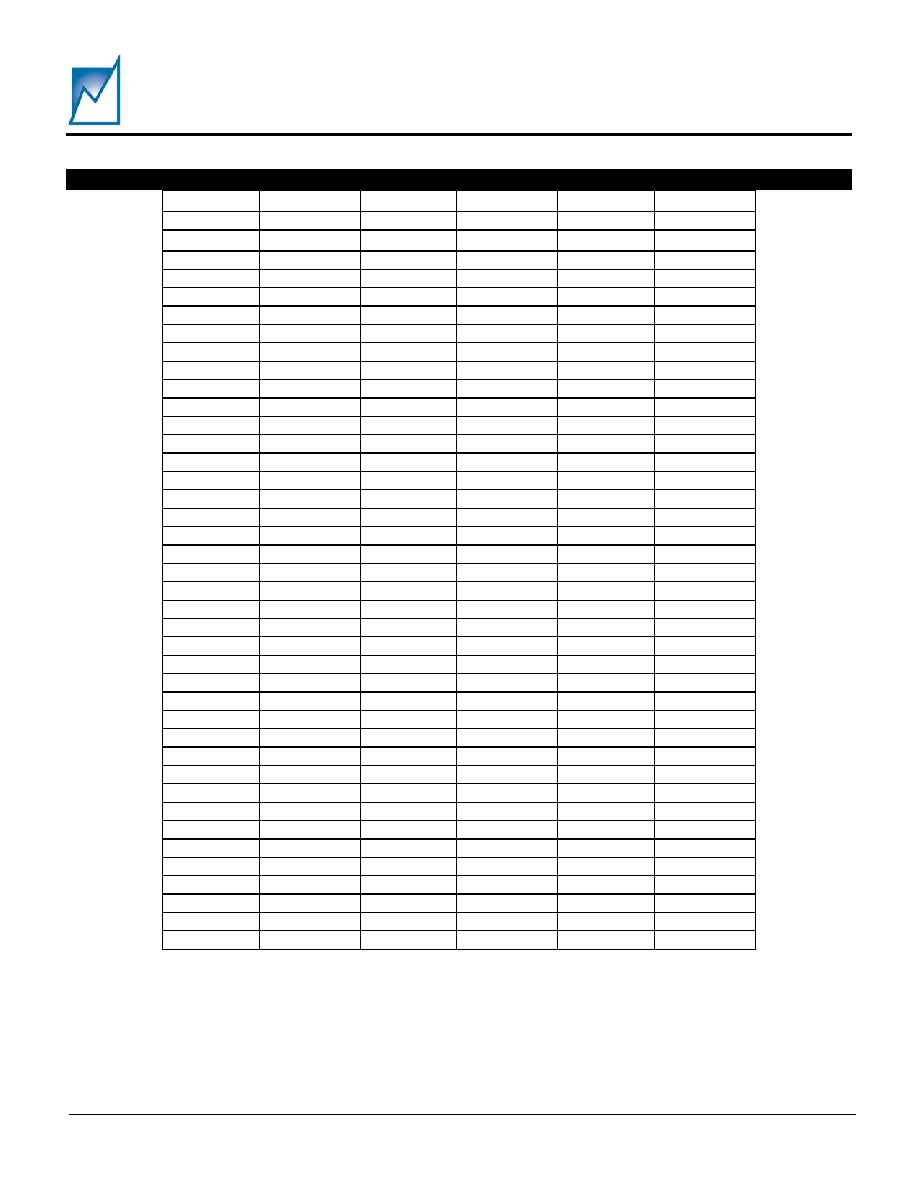
SMM764
Preliminary Information
Summit Microelectronics, Inc
2098 1.1 6/29/2005
28
DEFAULT CONFIGURATION REGISTER SETTINGS ≠ SMM764FC-285
Register Contents Register Contents Register Contents
R0 FD R82
82 RBA
02
R1 84 R83
66 RBB
23
R2 0E R84
2A RBC
03
R3 00 R85
CD RBD
E0
R4 0E R86
12 RBE
03
R5 80 R87
E1 RBF
E0
R6 0E R88
49 RC0
03
R7 C7 R89
D7 RC1
38
RC FF R8A
81 RC2 03
RD 00 R8B
C3 RC3 38
RE 05 R8C
2A RC4
01
RF 08 R8D
29 RC5
90
R10 7F R8E 12 RC6 01
R11 7F R8F 3D RC7 90
R12 7F R90 49 RC8 00
R13 7F R91 85 RC9 00
R30 FD R92 81 RCA 00
R31 6E R93 71 RCB 00
R32 0E R94 29 RCC 03
R33 DA R95 D7 RCD FF
R34 0E R96 11 RCE 03
R35 46 R97 EC RCF FF
R36 0E R98 49 RD0 00
R37
80 R99
48 RD1
00
R3C
00 R9A
81 RD2
00
R3D
12 R9B
33 RD3
00
R3E
50 R9C
29 RD4
03
R40 FD R9D 9A RD5 D8
R41 9D R9E 11 RD6 03
R42 8E R9F AE RD7 D8
R43 2D RB0 02 RE0 00
R44 0E RB1 67 RE0 00
R45 A2 RB2 02 RE1 3D
R46 0F RB3 52 RE2 00
R47
20 RB4
03 RE3
3D
R4C 00
RB5 FF RE4 00
R4D
12 RB6
03 RE5
3D
R4E 50 RB7 FF RE6 00
R80 4A RB8 02 RE7 3D
R81 7B RB9 23
RC1
The default device ordering number is SMM764FC-285. It is programmed with the register contents as shown above
and tested over the commercial temperature range with a VREF setting of 1.25V. Other standard external VREF
voltage settings that can be specified and tested are values of: 1.024, 1.225, 1.250, 2.048, 2.500, 3.000 or 3.300.
The value is derived from the customer supplied hex file. New device suffix numbers are assigned to non-default
requirements. If other VREF values are required, please contact a Summit Microelectronics Sales Representative.
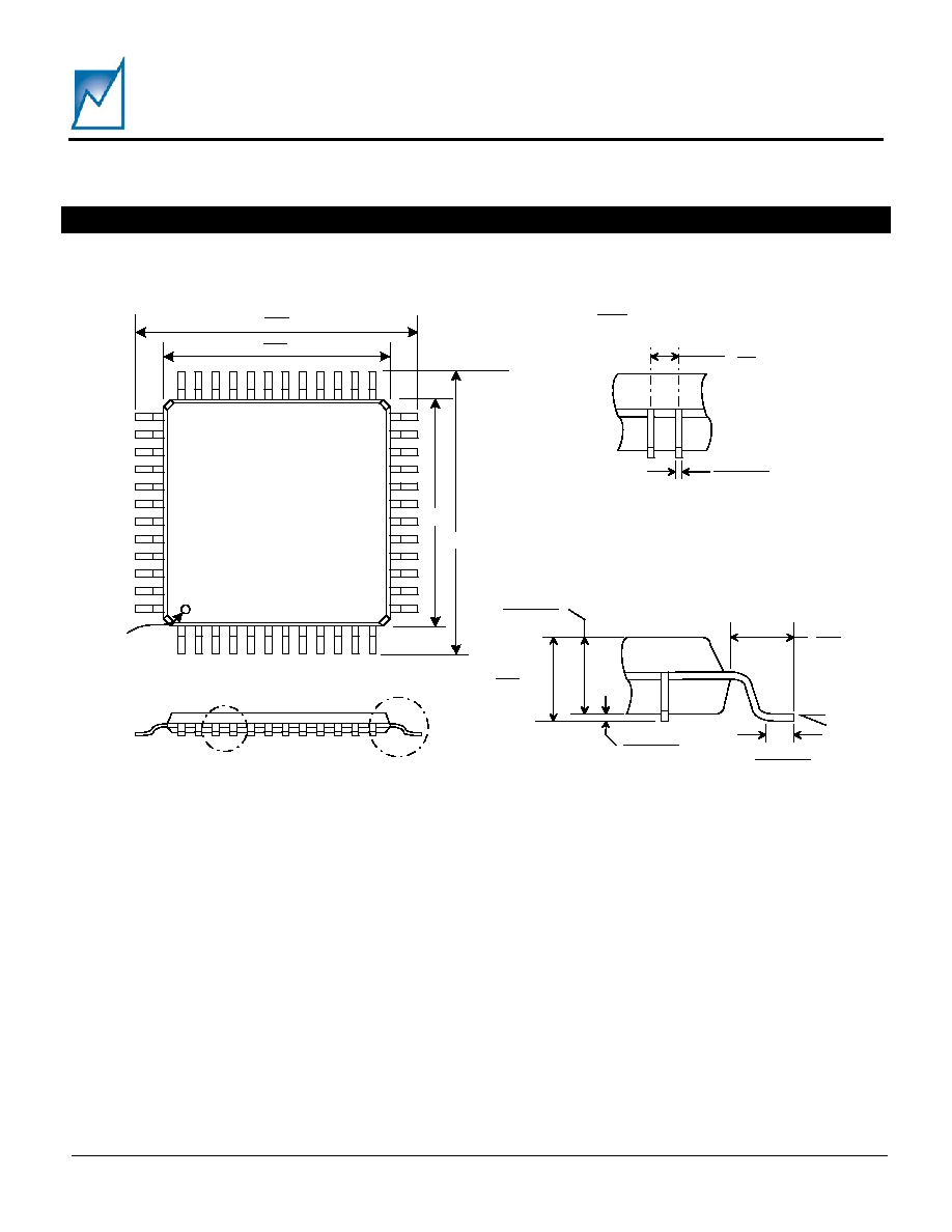
SMM764
Preliminary Information
Summit Microelectronics, Inc
2098 1.1 6/29/2005
29
PACKAGE
A
B
Pin 1
Indicator
Inches
(Millimeters)
0.002 - 0.006
(0.05-0.15)
MAX.
0.047
(1.2)
0.037 - 0.041
0.95 - 1.05
0.018 - 0.030
(0.45 - 0.75)
0.039
(1.00)
0.02
(0.5)
BSC
0.007 - 0.011
(0.17 - 0.27)
DETAIL "A"
DETAIL "B"
(B)
(A)
(A)
0.354
(9.00) BSC
0.276
(7.00)
BSC (B)
48 PIN TQFP PACKAGE
0
o
Min to
7
o
Max
Ref Jedec M S-026
Ref
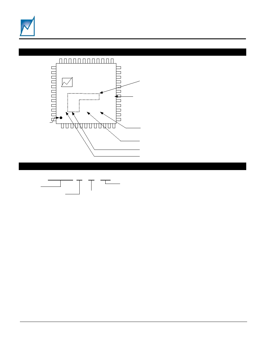
SMM764
Preliminary Information
Summit Microelectronics, Inc
2098 1.1 6/29/2005
30
PART MARKING
ORDERING INFORMATION
SUMMIT
SMM764F
AYYWW
Pin 1
Annn
Summit Part Number
Date Code (YYWW)
Part Number suffix
(Contains Customer specific ordering requirements)
Lot tracking code (Summit use)
Drawing not to scale
xx
Status Tracking Code
(Blank, MS, ES, 01, 02,...)
(Summit Use)
Product Tracking Code (Summit use)
SMM764
F
Package
F=48 Lead TQFP
Summit
Part
Number
Specific requirements are contained in the suffix such as
Hex code, Hex code revision, etc. The calibrated VREF voltage
settings are standard values of: 1.024, 1.225, 1.250, 2.048,
2.500, 3.000 or 3.300
nnn
Part Number Suffix (see page 28)
C
Temp Range
C=Commercial
Blank=Industrial
SMM764
Preliminary Information
Summit Microelectronics, Inc
2098 1.1 6/29/2005
31
Terms and Definitions
Fault-Triggered
This term refers to either a power-off or force-shutdown operation. When a UV, OV, or
sequence termination condition trigger a power-off or force-shutdown a fault triggered power-
off or force-shutdown is said to occur. This sets the restart delay at 2.4s, and can limit the
number of allowable retries. This term has no correlation to the FAULT pin.
Command-Triggered
This term refers to either a power-off or force-shutdown operation. When either the FS# or
PWR_ON pin is asserted or an I
2
C command is issued a Command-Triggered power-off or
force-shutdown is said to occur. This sets the restart delay at 12.5ms, and will not limit the
number of allowable retries.
ADOCTM
ADOC (Active DC Output Control) is a proprietary secondary closed loop compensation
control, used to maintain output voltages to ±0.2%.
Power-off
Power-off sequencing refers to cascaded power-off sequencing unless explicitly noted.
Cascaded power-off sequencing refers to a feedback based supply termination in which each
channel in the previous sequence position is monitored, and the monitored voltage must fall
below a programmable OFF threshold before the next sequence position is allowed to turn
off. Channels in the same sequence position are not capable of Cascaded power-off
sequencing.
Power-on
Power-off sequencing refers to cascaded power-off sequencing unless explicitly noted.
Cascaded power-off sequencing refers to a feedback based supply termination in which each
channel in the previous sequence position is monitored, and the monitored voltage must fall
below a programmable OFF threshold before the next sequence position is allowed to turn
off. Channels in the same sequence position are not capable of Cascaded power-off
sequencing.
Force-shutdown
When all supplies are immediately disabled without regard to sequence position, or any other
quantity.
Sequence-LinkTM
When more than one SMM764 or SMM766 derivatives are connected creating a seamless
multi-channel network.
UV
Programmed Under Voltage threshold for monitored channels and supplies
OV
Programmed Over Voltage threshold for monitored channels and supplies
UVLO
Undervoltage Lockout. Prevents voltage at VDD or 12VIN pin from powering the SMM764
until proper operating voltages have been reached.
Margin
The ability to change the nominal output voltage by use of trim pin.
ADC
Analog to Digital Converter. Converts analog voltage to digital voltage. SMM764 represents
all measured voltages by 10-bit digital reading.
Retries
The number of times the SMM764 will restart after a Fault-Triggered power-off or force-
shutdown.
Restart
When the SMM764 begins power on sequencing, includes initial power-on sequence.
Power-on delay
Delay from restart timer expiration to PUP
Y
pin active
Power-off delay
Programmable delay from VM
X
off to PUP
Y
inactive
Sequence
Termination
When a supply fails to reach its programmed UV, or OFF, threshold before expiration of
internal timer.
Monitoring
When any quantity including temperature, and voltage is converted to a digital value by the
ADC and compared against a user programmable setting.
GUI
Graphical user interface. Program that reads from and writes to non-volatile registers on the
SMM764 and displays results in accordance to register function.

SMM764
Preliminary Information
Summit Microelectronics, Inc
2098 1.1 6/29/2005
32
NOTICE
NOTE 1 - This is a Preliminary Information data sheet that describes a Summit product currently in pre-production with limited characterization.
Revision 1.1 - This document supersedes all previous versions. Data Sheet updates can be accessed by "right" or "left" mouse clicking on the link:
http://www.summitmicro.com/prod_select/summary/smm764.htm
Device Errata sheets can be accessed by "right" or "left" mouse clicking on the link:
http://www.summitmicro.com/errata/SMM764
SUMMIT Microelectronics, Inc. reserves the right to make changes to the products contained in this publication in order to improve design,
performance or reliability. SUMMIT Microelectronics, Inc. assumes no responsibility for the use of any circuits described herein, conveys no license
under any patent or other right, and makes no representation that the circuits are free of patent infringement. Charts and schedules contained
herein reflect representative operating parameters, and may vary depending upon a user's specific application. While the information in this
publication has been carefully checked, SUMMIT Microelectronics, Inc. shall not be liable for any damages arising as a result of any error or
omission.
SUMMIT Microelectronics, Inc. does not recommend the use of any of its products in life support or aviation applications where the failure or
malfunction of the product can reasonably be expected to cause any failure of either system or to significantly affect their safety or effectiveness.
Products are not authorized for use in such applications unless SUMMIT Microelectronics, Inc. receives written assurances, to its satisfaction, that:
(a) the risk of injury or damage has been minimized; (b) the user assumes all such risks; and (c) potential liability of SUMMIT Microelectronics, Inc.
is adequately protected under the circumstances.
© Copyright 2005 SUMMIT MICROELECTRONICS, Inc.
PROGRAMMABLE ANALOG FOR A DIGITAL WORLDTM
ADOC
TM
and Sequence-Link
TM
are registered trademarks of Summit Microelectronics Inc., I2C is a trademark of Philips Corporation.
SMM764
Preliminary Information
Summit Microelectronics, Inc
2098 1.1 6/29/2005
33
Document Rev.
Description
Date
Owner
1.0 Preliminary
datasheet
JJ
1.1
VIH & VIL modified for 0.8 VIH and 0.2 VIL logic levels.
TRIM CAP description changed to be left floating when
unused.
6/29/2005 JJ