 | –≠–ª–µ–∫—Ç—Ä–æ–Ω–Ω—ã–π –∫–æ–º–ø–æ–Ω–µ–Ω—Ç: SMP9212 | –°–∫–∞—á–∞—Ç—å:  PDF PDF  ZIP ZIP |
Advance Information page 1 of 1
SMP9210 SMP9211 SMP9212
SUMMIT
MICROELECTRONICS, Inc.
FEATURES
∑
Two 10-bit Nonvolatile DACs
-
INL
±
1LSB
-
DNL:
±
1LSB
∑
Programmable Configuration
∑
Programmable Power-on Reset Options
-
Recall Full Scale Value
-
Recall Zero Scale Value
-
Recall Mid-Scale Value
-
Recall NV Register Value
∑
Tandem or Independent Operation of DACs
∑
Power-down mode (short V
OUT
to gnd)
OVERVIEW
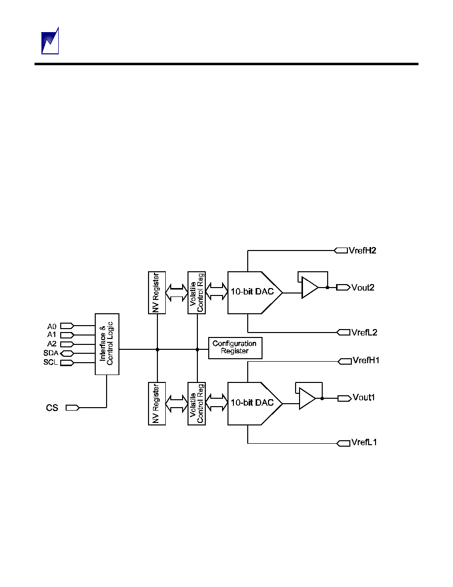
The SMP9210 is a serial input, voltage output, dual
10-bit digital to analog converter. It can operate from
a single +2.7V to +5.5V supply. Internal precision
buffers swing rail-to-rail with an input reference range
from ground to the positive supply.
The SMP9210 integrates two 10-bit DACs and their
associated circuits that include; an enhanced unity
gain operational amplifier output, a 10-bit volatile data
latch, a 10-bit nonvolatile data register and an
industry standard 2-wire serial interface.
Dual 10-bit Nonvolatile DAC
In-system Programmable Analog
BLOCK DIAGRAM
I
I
S
S
P
P
a
a
TM

Advance Information page 2 of 2
SMP9210 SMP9211 SMP9212
SUMMIT
MICROELECTRONICS, Inc.

Advance Information page 3 of 3
SMP9210 SMP9211 SMP9212
SUMMIT
MICROELECTRONICS, Inc.
SMP9210
Signal
Pin
Function
A2
1
Address Pin A2
A1
2
Address Pin A1
A0
3
Address Pin A0
V
REFH
2
4
DAC2 VREFH Input
V
REFL
2
5
DAC2 VREFL Input
V
OUT
2
6
DAC2 V
OUT
Gnd
7
Ground
CS
8
Chip Select
V
OUT
1
DAC1 V
OUT
V
REFL
1
10 DAC1 VREFL Input
SCL
11 Serial Clock Input
V
REFH
1
12 DAC1 VREFH Input
V
DD
13 Supply Voltage
SDA
14 Bi-directional Serial Data
SMP9211
Signal
Pin
Function
A2
1
Address Pin A2
A1
2
Address Pin A1
A0
3
Address Pin A0
V
REFH
2
4
DAC2 VREFH Input
V
REFL
2
5
DAC2 VREFL Input
V
OUT
2
6
DAC2 V
OUT
Gnd
7
Ground
MUTE
8
Mute Input
V
OUT
1
DAC1 V
OUT
V
REFL
1
10 DAC1 VREFL Input
SCL
11 Serial Clock Input
V
REFH
1
12 DAC1 VREFH Input
V
DD
13 Supply Voltage
SDA
14 Bi-directional Serial Data
SMP9212
Signal
Pin
Function
A2
1
Address Pin A2
A1
2
Address Pin A1
A0
3
Address Pin A0
V
REFH
2
4
DAC2 VREFH Input
V
REFL
2
5
DAC2 VREFL Input
V
OUT
2
6
DAC2 V
OUT
Gnd
7
Ground
V
REF
8
Reference Voltage Output
V
OUT
1
DAC1 V
OUT
V
REFL
1
10 DAC1 VREFL Input
SCL
11 Serial Clock Input
V
REFH
1
12 DAC1 VREFH Input
V
DD
13 Supply Voltage
SDA
14 Bi-directional Serial Data

Advance Information page 4 of 4
SMP9210 SMP9211 SMP9212
SUMMIT
MICROELECTRONICS, Inc.
PIN DESCRIPTION
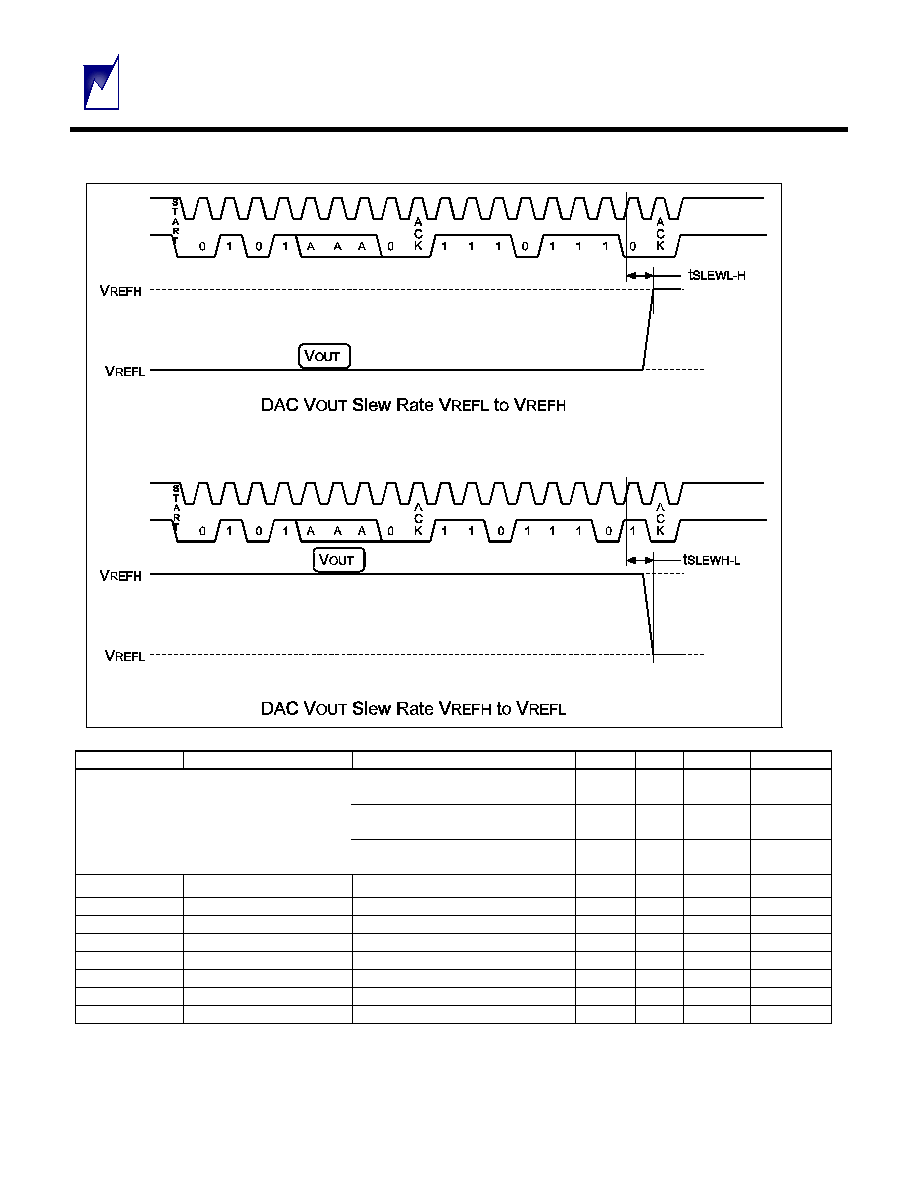
GND is the device ground pin.
V
OUT
is the voltage output of the DACs. It is
buffered by a unity-gain follower that can slew up to
1V/s.
VREFL is the lower of the voltage reference
inputs. VREFL must be equal to or greater than
ground and less than VREFH.
VREFH is the higher of the voltage reference
inputs. VREFH must be equal to or less than VCC
and greater than VREFL.
A0, A1 and A2 are the address inputs to the
SMP9210 serial interface logic. Biasing the address
inputs will determine the device's bus address that is
contained within the serial data stream when
communication over the serial bus.
SCL is the serial interface clock. It is used to
clock data into and out of the SMP9210. When
writing to the device, data must remain stable while
SCL is HIGH. When reading, data is clocked out of
the SMP9210 on the falling edge of SCL.
SDA is a bi-directional pin used to transfer data
into and out of the SMP9210.
Pin 8 is a multifunction pin and is in-system
programmable by the customer or it can be
configured by Summit prior to shipment. It can
function as Chip Select input (V
IH
= selected), a
MUTE input (V
IH
= mute) or as a Vref output (1.25V).
Device Operation
The SMP9210 has two, 10-bit, digital to analog
converters that are comprised of a resistor network
that converts 10-bit digital inputs into equivalent
analog output voltages in proportion to the applied
reference voltages. The voltage differential between
the VREFL and VREFH inputs sets the full-scale
output voltage for its respective DAC.
Each DAC has a 10-bit volatile register that
holds the digital value decoded by the DAC into an
analog voltage output. The register can be written
directly via the serial interface, commanded to load
the zero scale value, full scale value or mid-scale
value or recall a preset value stored in a nonvolatile
register.
Each DAC has a 10-bit nonvolatile register that
can hold a 'set-and-forget' value that can be recalled
whenever the device is powered-on.
The SMP9210 also has a nonvolatile
configuration register that is accessible over the 2-
wire bus. The configuration register is used to
select the device type identifier, the function of pin 8
and the DAC power-on state.
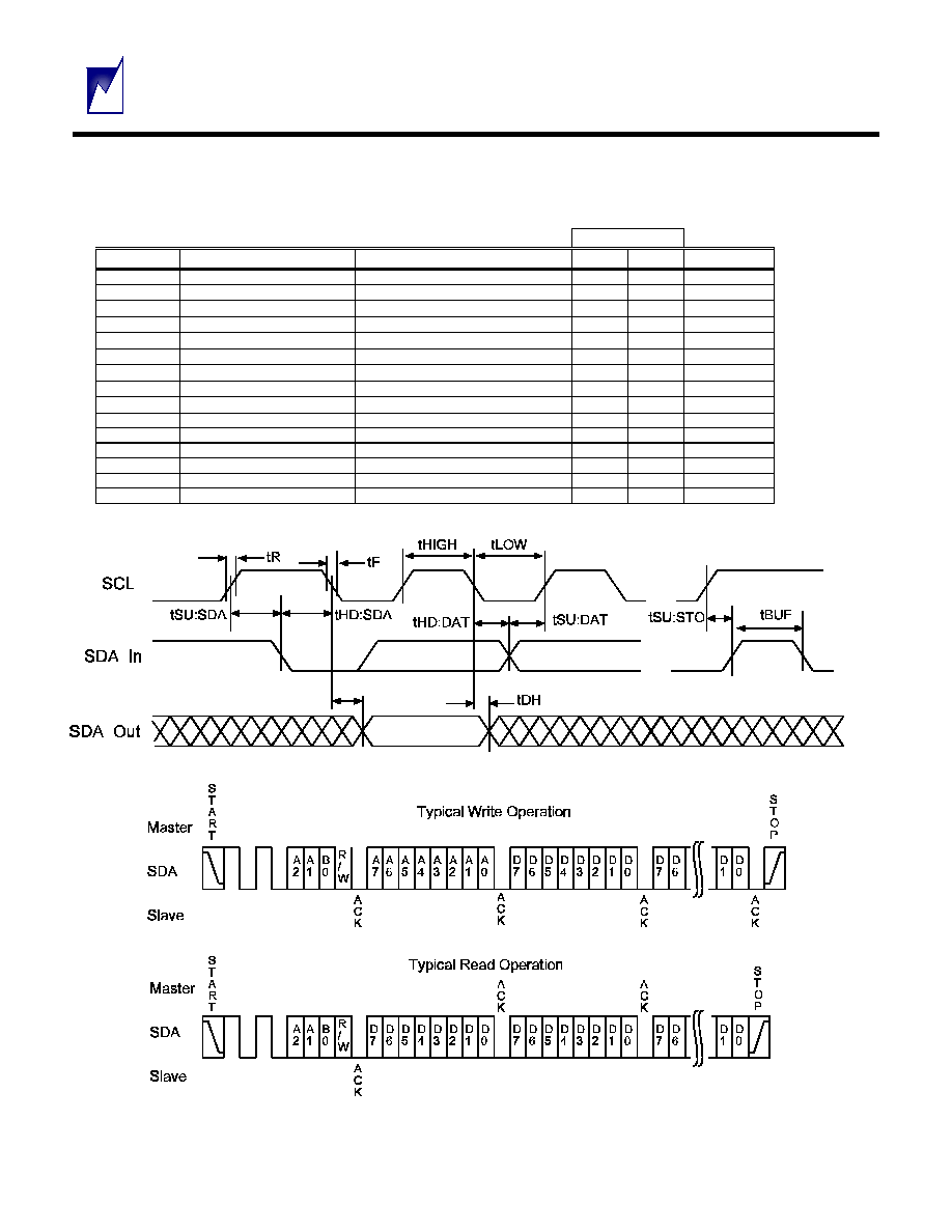
Accessing the DACs
The SMP9210 uses the industry standard 2-wire
serial protocol. The bus is designed for two-way,
two-line serial communication between different
integrated circuits. The two lines are the SCL (serial
clock) and SDA (serial data) and both lines must be
tied to the positive supply through a pull-up resistor..
The protocol defines devices as being either masters
or slaves, the SMP9210 will always be a slave in that
it does not initiate any communications or provide a
clock output.
Data transfers are initiated when a master
issues a 'start' condition, which is a high to low
transition on SDA while SCL is high. The start is
immediately followed by an eight bit transmission:
bits 7:1 comprise the device type identifier and bus
device bus address; bit 0 is the read/write bit
indicating the action to follow. If the intended device
receives the byte and recognizes its address it will
return an acknowledge during the 9
th
clock cycle.
Some data transfers will be concluded with a 'stop'
condition, which is a low to high transition on SDA
while SCL is high. Note: a stop condition must be
performed for all nonvolatile write operations.
Addressing Convention
0
1
0
1
A
2
A
1
A
0
R/
W
S
T
A
R
T
A
C
K
The DAC device type identifier default is
0101[b]. In order to accommodate more than eight
devices on a single bus, the device type identifier can
by modified by the end user by writing to the
configuration registers.
The command structure is illustrated in Table 1.
Of special note is the ability to write individually to the
two DACs or write to them in tandem. The first three
commands are three bytes in length and can either
be volatile or nonvolatile.
The 'Zero' commands load all zeroes into the
DAC registers forcing the V
OUT
to VREFL. The 3F
commands load all ones into the DAC registers,
forcing V
OUT
to VREFH. The Recall commands, write
the nonvolatile register value into the DAC registers.
The PD commands connect V
OUT
to GND. These
four commands are all two bytes; the device
Advance Information page 5 of 5
SMP9210 SMP9211 SMP9212
SUMMIT
MICROELECTRONICS, Inc.
type/address byte followed by the command byte.
They are will be enforced with or without a stop being
issued and the new register value is never stored in
the nonvolatile register.
Writing a value to a DAC can either be a write to the
DAC register only or a combined write to both the
DAC Register and its nonvolatile register. They are
identical with the one exception being the register
write does not entail issuing a stop condition;
whereas, the nonvolatile write operation is concluded
with a stop.
The sequence is to issue a start, followed by the
device type and bus address, with the read/write bit
set to zero. The SMP9210 will respond with an
acknowledge and the master will then issue the
command and follow-on data. In the example below
the write is to DAC1, where the command = 1001[b];
the dc bits are don't care, D9 and D8 are the MSBs of
the DAC value being written. The SMP9210 will then
respond with an acknowledge followed by the master
writing the last eight bits. In the first example shown,
no stop is generated after the SMP9210
acknowledge; therefore, the write is only to the
register. In the second example the SMP9210
acknowledge is followed by a stop; therefore, the
data is written to both the DAC register and to the
nonvolatile register.
Table 1. Command Structure.
MSB
LSB
7
6
5
4
3
2
1
0
Command
Function
1
0
0
1
dc
dc
D9
D8
Write DAC1
Write 10-bit value to DAC1
1
0
1
0
dc
dc
D9
D8
Write DAC2
Write 10-bit value to DAC2
1
0
1
1
dc
dc
D9
D8
Write Both DACS
Write the same 10-bit value to DAC1
and DAC2
1
1
0
1
1
1
1
0
ZeroDAC1
Set DAC1 to Zero Scale (V
REFL
)
1
1
0
1
1
1
0
1
ZeroDAC2
Set DAC2 to Zero Scale (V
REFL
)
1
1
0
1
1
1
1
1
ZeroBOTH
Set DAC1 & DAC2 to Zero Scale (V
REFL
)
1
1
1
0
1
1
1
0
3FDAC1
Set DAC1 to Full Scale (V
REFL
)
1
1
1
0
1
1
0
1
3FDAC2
Set DAC2 to Full Scale (V
REFL
)
1
1
1
0
1
1
1
1
3FBOTH
Set DAC1 & DAC2 to Full Scale (V
REFL
)
1
1
1
1
dc
dc
1
0
RecallDAC1
Recall E
2
to DAC1
1
1
1
1
dc
dc
0
1
RecallDAC2
Recall E
2
to DAC2
1
1
1
1
dc
dc
1
1
RecallBoth
Recall E
2
to Both DACs
1
0
0
0
dc
dc
1
0
PDDAC1
Power Down DAC1 (V
OUT
to GND)
1
0
0
0
dc
dc
0
1
PDDAC2
Power Down DAC2 (V
OUT
to GND)
1
0
0
0
dc
dc
1
1
PDBOTH
Power Down Both DACs (V
OUT
to GND)
*dc = don't care
Writing to DACs Data Sequence (Volatile Write)
0
1
0
1
A
2
A
1
A
0
0
1
0
0
1
d
c
d
c
D
9
D
8
D
7
D
6
D
5
D
4
D
3
D
2
D
1
D
0
A
C
K
A
C
K
S
t
a
r
t
Device Type and Bus Address
W
Command
A
C
K
Writing to DACs Data Sequence (Nonvolatile Write)
0
1
0
1
A
2
A
1
A
0
0
1
0
0
1
d
c
d
c
D
9
D
8
D
7
D
6
D
5
D
4
D
3
D
2
D
1
D
0
S
t
a
r
t
A
C
K
A
C
K
A
C
K
S
t
o
p
Command Sequence (
example command shown 3FDAC1
)
0
1
0
1
A
2
A
1
A
0
0
1
1
1
0
1
1
1
0
S
t
a
r
t
Device Type and Bus Address
W
A
C
K
Command
A
C
K

Advance Information page 6 of 6
SMP9210 SMP9211 SMP9212
SUMMIT
MICROELECTRONICS, Inc.
The third example illustrates the data sequence
for a two-byte command.
Special Configurations
The SMP9210 can be configured by the end
user or by Summit prior to shipment. There is one
configuration register and it is accessed through the
serial interface using 1001[b] as the device type
address. The register is shown below.
MSB
LSB
7 6 5 4 3 2 1 0
A
3
A
2
A
1
A
0
L
o
r
H
Z
P
O
R
1
P
O
R
0
L
O
C
K
x x x x x x x 0 Config Register
Accessible
x x x x x x x 1 Config Register Locked
x x x x x 0 0 Power-on Recall all 0's
x x x x x 0 1 Power-on Recall all 1's
x x x x x 1 0 Power-on Recall Mid Scale
x x x x x 1 1 Power-on Recall NV-
Register
x x x x 0 V
OUT
= Low Z on Power-Down
x x x x 1 V
OUT
= High Z on Power-Down
A A A A Programmable DAC Device Type
Address
Bit 0 - When bit 0 is written as a 1 the configuration
register will be locked and it will become inaccessible
for reading and writing.
Bits 2:1 are use to select the power-on recall value to
be loaded into the DAC registers.
Bit 3 selects the power down option for the V
OUT
pins.
Bits 7:4 can be used to program unique DAC device
type identifiers. When the default 0101 is used the
number of SMP9210's allowed on a single bus is
limited to eight. This can be expanded infinitely if the
CS input is also used. The only drawback is the
decoding or use of port pins to drive the CS inputs. If
we assume no other devices on the bus and that
each DAC device type address is utilized, then the
end user can effectively have 256 individually
addressable devices on a single bus. Now,
combining this capability with the CS pin a microC
can enable blocks of 256 SMP9210's vs blocks of 8.

Advance Information page 7 of 7
SMP9210 SMP9211 SMP9212
SUMMIT
MICROELECTRONICS, Inc.
DAC Analog Characteristics
Symbol
Parameter
Condition
Min.
Type.
Max
Units
Static Performance
N
Resolution
10
Bits
INL
Relative Accuracy
-1.0
+/-0.5
+1.0
LSB
DNL
Differential Nonlinearity
GUARANTEED MONOTONIC
-1
+/-0.5
+1
LSB
VZSE
Zero Scale Error
Data = 000H
0
5
mV
VFS
Full Scale Voltage
Data = 3FFH
VrefH
V
TCV
Full-Scale Tempco
=/-15
ppm
MATCHING PERFORMANCE
Linearity Matching Error
+/-1
LSB
ANALOG OUTPUT
IOUT
Output Current
Data = 200H,
Vout ,3LSB
+/-5
mA
LDREG
Load Regualtion @
Halfscale
RL = 1K
to infinity, Data = 200H
1
3
LSB
CL
Capacitive Load
No Oscillation
500
pF
Dynamic characteristics
BW_10K Bandwidth ≠3dB
R = 10K
100
kHZ
THD
Total Harmonic Distortion VA=1Vrms ,f=1KHz,
0.08
%
Channel to Channel
Isolation
f = 1KHz
VIN = 100mV p-p on VrefH
-60
dB
Digital Cross Talk
-60
dB
Reference Voltages
VrefH
VrefH > VrefL
Gnd+?
VCC
V
VrefL
VrefL < VrefH
Gnd
VCC-?
V
Power
ISY
VDD Supply Current
VDD = +5V, excludes Iref
100
µ
A
Iref
Reference Voltage Current
100
µ
A
VSY
Supply Voltage
2.7
5.5
V
Advance Information page 8 of 8
SMP9210 SMP9211 SMP9212
SUMMIT
MICROELECTRONICS, Inc.
Symbol
Parameter
Condition
Min.
Typ.
Max.
Units
I
DD
Power Supply Current
NV Write V
DD
= 5.5V
V
DD
= 2.7V
mA
Standby or Quiescent
Excluding Current V
DD
= 5.5V
Through DACs V
DD
= 2.7V
µ
A
Power Down
Total Current V
DD
= 5.5V
Including DAC V
DD
= 2.7V
µ
V
DD
Supply Voltage
2.7
5.5
V
V
IH
SDA, SCL
0.7xV
DD
V
V
IL
SDA, SCL
0.3xV
DD
V
V
OL
SDA
I
OL
= 3mA
0.4
V
I
LI
Input Leakage
VIN = 0 to V
DD
10
mA
I
LO
Output Leakage
VOUT = 0 to V
DD
W
END
Write Endurance
Number of NV Store Operations
1x10
6
NVStores
t
DR
Data Retention
NVData Retention
100
Years
Advance Information page 9 of 9
SMP9210 SMP9211 SMP9212
SUMMIT
MICROELECTRONICS, Inc.
AC Operating Characteristics
(Over Recommended Operating Conditions)
2.7V to 5.5V
Symbol
Parameter
Conditions
Min. Max.
Units
fSCL
SCL Clock Frequency
0
100
KHz
tLOW
Clock Low Period
4.7
µ
s
tHIGH
Clock High Period
4.0
µ
s
tBUF
Bus Free Time
Before New Transmission
4.7
µ
s
tSU:STA
Start Condition Setup Time
4.7
µ
s
tHD:STA
Start Condtion Hold Time
4.0
µ
s
tSU:STO
Stop Condition Setup Time
4.7
µ
s
tAA
Clock Edge to Valid Output
SCL low to Valid SDA (cycle n)
0.3
3.5
µ
s
tDH
Data Out Hold Time
SCL low (cycle n+1) to SDA change
0.3
µ
s
tR
SCL and SDA Rise Time
1000
ns
tF
SCL and SDA Fall Time
300
ns
tSU:DAT
Data In Setup Time
250
ns
tHD:DAT
Data In Hold Time
0
ns
TI
Noise Filter SCL & SDA
Noise Suppression
100
ns
tWR
Write Cycle Time
5
ms

Advance Information page 10 of 10
SMP9210 SMP9211 SMP9212
SUMMIT
MICROELECTRONICS, Inc.
Ordering Information
SMP9210S 14 lead SOIC
SMP9211S 14 lead SOIC
SMP9212S 14 lead SOIC