 | –≠–ª–µ–∫—Ç—Ä–æ–Ω–Ω—ã–π –∫–æ–º–ø–æ–Ω–µ–Ω—Ç: SMP9517P | –°–∫–∞—á–∞—Ç—å:  PDF PDF  ZIP ZIP |
© SUMMIT MICROELECTRONICS, Inc. 2000 ∑ 300 Orchard City Drive, Suite 131 ∑ Campbell, CA 95008 ∑ Phone 408-378-6461 ∑ Fax 408-378-6586 ∑ www.summitmicro.com
1
Characteristics subject to change without notice
SUMMIT
MICROELECTRONICS, Inc.
2035 3.0 5/10/00
SMP9517
FEATURES
Digitally Controlled Electronic Potentiometer
∑
7-Bit Digital-to-Analog Converter (DAC)
≠ Independent Reference Inputs
≠ Differential Non-Linearity of ±0.5LSB max
≠ Integral Non-Linearity of ±1LSB max
∑
V
OUT
Value in EEPROM for Power-On Recall
≠ Equivalent to 128-Step Potentiometer
∑
Unity Gain Op Amp Drives up to 1mA
∑
Simple Trimming Adjustment
≠ Debounced Pushbutton Interface
∑
Low Noise Operation
∑
"Clickless" Transitions between DAC Steps
∑
No Mechanical Wear-out Problem
≠ 1,000,000 Stores (typical)
≠ 100 Year Data Retention
∑
Operation from 2.7V to 5.5V Supply
∑
Low Power: 1mW max at 5V
Nonvolatile DACPOTTM Electronic Potentiometer
With Debounced Push Button Interface
OVERVIEW
The SMP9517 DACPOT trimmer is an 7-bit nonvolatile
DAC designed to replace mechanical potentiometers.
The SMP9517 includes a unity-gain amplifier to buffer the
DAC output and enables V
OUT
to swing from rail to rail.
The DACPOT trimmer operates over a supply voltage
range of 2.7V to 5.5V.
The SMP9517's simple pushbutton input provides an ideal
interface for operator adjusted equipment. This interface
allows for quick and easy adjustment of even the most
sophisticated systems.
The SMP9517 is a pin-compatible performance upgrade
for other industry nonvolatile potentiometers. For higher
resolution applications the pin-compatible S9518 pro-
vides 256 steps with the same pushbutton interface. Both
the SMP9517 and the S9518 provide `clickless' transitions
of V
OUT
.
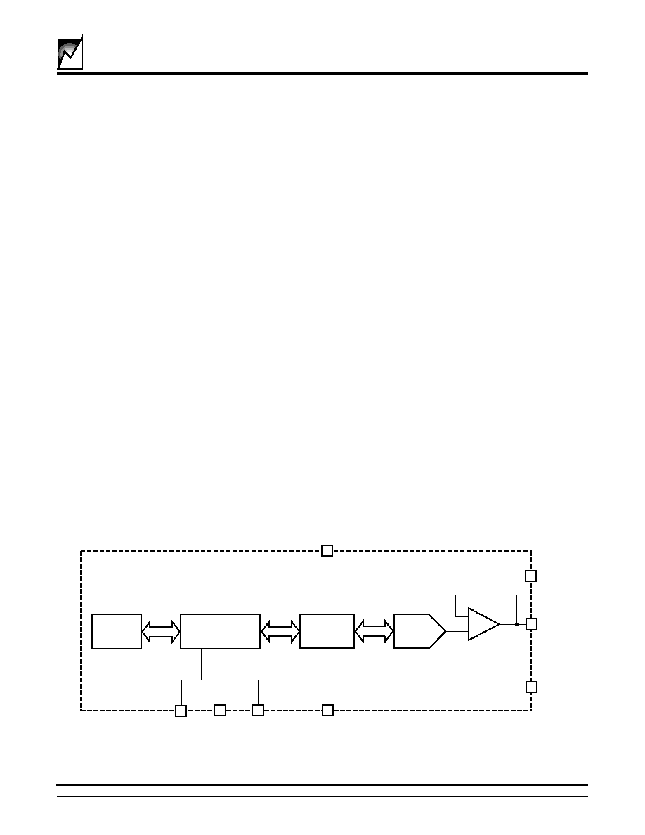
FUNCTIONAL BLOCK DIAGRAM
DWN#
VDD
8
2
VOUT
5
7-Bit
E2PROM
VL
6
VH
3
7-Bit Data
Register
Debounce Circuit
& Write Control
Logic
7-Bit DAC
UP#
1
STR#
7
GND
4
2035 T BD 3.0
2
SMP9517
SUMMIT MICROELECTRONICS, Inc.
2035 3.0 5/10/00
Analog Section
The SMP9517 is an 7-bit, voltage output digital-to-analog
converter (DAC). The DAC consists of a resistor network
that converts 7-bit digital values into equivalent analog
output voltages in proportion to the applied reference
voltage.
Reference Inputs
The voltage differential between the V
L
and V
H
inputs sets
the full-scale output voltage range. V
L
must be equal to or
greater than ground (a positive voltage). V
H
must be
greater than V
L
and less than or equal to V
DD
. See
specifications for guaranteed operating limits.
Output Buffer Amplifier
The voltage output is from a precision unity-gain follower
that provides a rail-to-rail output swing.
Digital Interface
The interface provides simple pushbutton control of an
up/down counter that drives the DAC. The DAC output is
a ratiometric voltage output.
UP# is an active low pushbutton input. An internal pull-up
resistor, with nominal value of 50k
, eliminates an exter-
nal resistor. A 30ms debounce period is included in the
input timing to prevent multiple pulsing of the counter.
Either a switch closure to ground or a low logic level will,
after the debounce time, change the potentiometer tap
position. UP# moves the output voltage towards the V
H
reference input.
If the UP# pushbutton is kept depressed the counter will
continue to increment at the rate of one count every
250ms for one second. After one second the counter
increments faster, one count every 50ms, until the
pushbutton is released. Changes to the DAC output using
the UP# input do not alter the data stored in EEPROM.
PINOUT
DWN# is an active low pushbutton input that decrements
the counter and moves the potentiometer output voltage
towards the V
L
reference input. The DWN# control input
also includes an internal 50k
pull-up resistor and a 30ms
debounce period to prevent multiple pulsing. A low logic
level will also change the potentiometer tap position after
the debounce period.
If the DWN# pushbutton is kept depressed the counter
continues to decrement at the rate of one count every
250ms for one second. After one second the counter
decrements at one count every 50ms until the pushbutton
is released. Changes to the DAC output using the DWN#
input do not alter the data stored in EEPROM.
STR# This input can be used in two ways:
1) If the input is tied low, then AUTOSTORE is enabled.
When V
DD
powers down, an automatic store cycle
takes place that updates the nonvolatile EEPROM
memory.
2) STR# is an active low pushbutton input that also
updates the nonvolatile memory. The input is
debounced but does not have an internal pull-up
resistor. For every valid push the SMP9517 will store
the current potentiometer position to EEPROM.
PIN NAMES
2035 Table01 3.0
l
o
b
m
y
S
n
o
i
t
p
i
r
c
s
e
D
#
P
U
V
s
e
v
o
m
,
t
u
p
n
i
B
P
T
U
O
V
d
r
a
w
o
t
H
t
u
p
n
i
#
N
W
D
V
s
e
v
o
m
,
t
u
p
n
i
B
P
T
U
O
V
d
r
a
w
o
t
L
t
u
p
n
i
V
H
V
F
E
R
h
g
i
h
D
N
G
d
n
u
o
r
G
V
T
U
O
t
u
p
t
u
o
e
g
a
t
l
o
v
d
e
m
m
i
r
T
V
L
V
F
E
R
w
o
l
#
R
T
S
t
u
p
n
i
l
o
r
t
n
o
c
a
g
n
i
d
i
v
o
r
p
,
t
u
p
n
i
e
r
o
t
S
n
o
i
t
a
r
e
p
o
e
r
o
t
s
a
e
t
a
i
t
i
n
i
o
t
V
D
D
)
V
5
.
5
o
t
V
7
.
2
(
e
g
a
t
l
o
v
y
l
p
p
u
S
UP#
DWN#
VH
GND
VDD
STR#
VL
VOUT
1
2
3
4
8
7
6
5
8-Pin PDIP
or 8-Pin SOIC
2035 T PCon 3.0

SMP9517
3
SUMMIT MICROELECTRONICS, Inc.
2035 3.0 5/10/00
There are five main blocks to the SMP9517: an 7-bit
EEPROM memory; input debounce circuits, control logic,
and 7-bit counter; 7-bit data register; decode section and
resistor ladder (DAC); and the buffer amplifier.
The input control section operates just like an up/down
counter. The output of this counter is fed to the data
register and then decoded to activate one of 127 electronic
switches connected to the resistor ladder. The ladder is
comprised of 128 resistors of equal value connected in
series. At the bottom of the ladder and at the junctions of
the resistors there are electronic switches that transfer the
voltage at each point to the buffer amplifier and then to the
output.
The SMP9517 is designed to interface directly to two
pushbutton switches that effectively move the potentiom-
eter wiper up or down. The UP# and DWN# inputs,
respectively, increment or decrement the 7-bit counter.
The data input to the DAC is decoded to select one of the
128 wiper positions along the resistive ladder. The wiper
increment input UP# and the wiper decrement input
DWN# are connected to internal pull-ups so that they
normally remain high. When pulled low by an external
pushbutton switch or a logic low level input, the wiper will
be switched to the next adjacent tap position. Internal
debounce circuitry prevents inadvertent switching of the
wiper position if UP# or DWN# remain low for less than
30ms (typical).
Each of the buttons can be pushed either once for a single
increment/decrement or held low continuously for multiple
increments/decrements. The number of increments/dec-
rements of the wiper position depends on how long the
button is pushed. When making a continuous push, after
the first second, the increment/decrement speed in-
creases. For the first second the device will be in the slow
scan mode. Then, if the button is held for longer than one
second, the device will go into the fast scan mode. As soon
as the button is released the SMP9517 will return to a
standby condition.
The DAC, whether set to 00
HEX
or FF
HEX
, acts like its
mechanical equivalent and does not move beyond the last
position. That is, the counter does not wrap around when
clocked up to FF
HEX
or down to 00
HEX
.
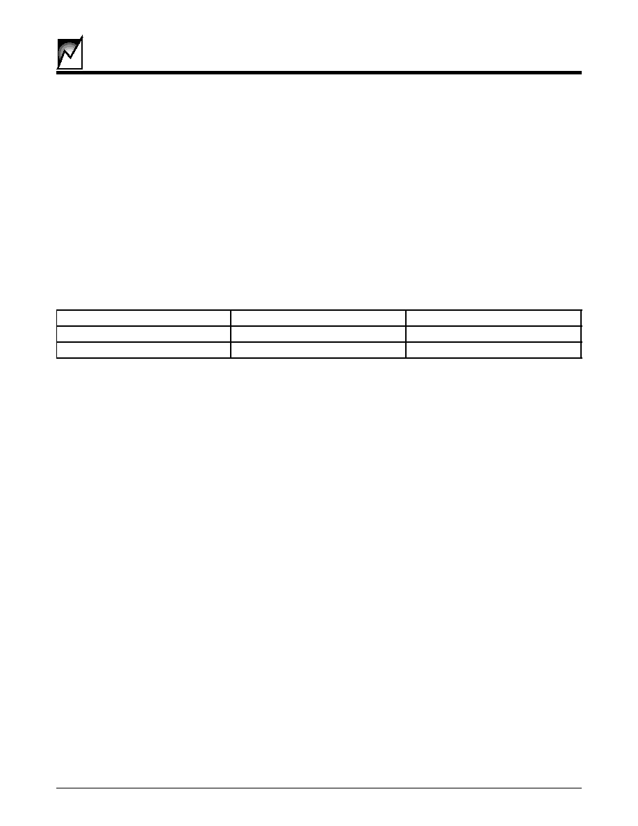
AUTOSTORE
The value of the counter is stored in EEPROM memory
whenever the chip senses a power-down of V
DD
while
STR# is enabled (held low). When power is restored the
contents of the memory are recalled and the counter reset
to the last value stored. If AUTOSTORE is to be imple-
mented, STR# is typically hard wired to GND. If STR# is
held high during power-up and then taken low the wiper will
not respond to the UP# or DWN# inputs until STR# is
brought high and the store is complete. See Figure 1.
Manual (Pushbutton) Store
When STR# is not enabled (held high) a pushbutton switch
may be used to pull STR# low and released to perform a
manual store of the wiper position in EEPROM memory.
See Figure 2.
Effect of V
DD
Removal
The resistor ladder, connected between V
H
and V
L
, does
not change value when V
DD
is removed. However, the
buffer amplifier no longer functions, and consequently a
high impedance appears at the V
OUT
pin.
Figure 2: Typical circuit with STR store pin
controlled by push button switch
Figure 1: Typical circuit with STR store pin used in
AUTOSTORE mode
DEVICE OPERATION
UP#
DWN#
VH
GND
VDD
STR#
VL
VOUT
8
7
6
5
1
2
3
4
VDD
3.3µF
2035 T Fig01 3.0
UP#
DWN#
VH
GND
VDD
STR#
VL
VOUT
8
7
6
5
1
2
3
4
VDD
20k
2035 T Fig02 3.0
4
SMP9517
SUMMIT MICROELECTRONICS, Inc.
2035 3.0 5/10/00
ABSOLUTE MAXIMUM RATINGS
Temperature Under Bias
≠55∞C to 125∞C
Storage Temperature
≠65∞C to 150∞C
Voltage on pins with reference to GND:
Analog Inputs
≠0.5V to V
DD
+0.5V
Digital Inputs
≠0.5V to V
DD
+0.5V
Analog Outputs
≠0.5V to V
DD
+0.5V
Digital Outputs
≠0.5V to V
DD
+0.5V
Lead Solder Temperature (10s)
300∞C
COMMENT
Stresses above those listed under Absolute Maximum
Ratings may cause permanent damage to the device.
These are stress ratings only, and functional operation of
the device at these or any other conditions outside those
listed in the operation sections of this specification is not
implied. Exposure to any absolute maximum rating for
extended periods may affect device performance and
reliability.
RECOMMENDED OPERATING CONDITIONS
n
o
i
t
i
d
n
o
C
.
n
i
M
.
x
a
M
e
r
u
t
a
r
e
p
m
e
T
C
∫
0
4
≠
C
∫
5
8
V
D
D
V
7
.
2
V
5
.
5
2035 Table02 3.0
SMP9517
5
SUMMIT MICROELECTRONICS, Inc.
2035 3.0 5/10/00
RELIABILITY CHARACTERISTICS
2035 Table03 3.0
Symbol
Parameter
Conditions
Min.
Typ.
Max.
Units
Accuracy
INL
Integral Non-Linearity
I
LOAD
= 100µA,
0.5
±1
LSB
DNL
Differential Non-Linearity
I
LOAD
= 100µA,
0.1
±0.5
LSB
Guaranteed but not tested
References V
H
V
REFH
Input Voltage
V
REFL
V
DD
V
V
L
V
REFL
Input Voltage
Gnd
V
REFH
V
R
IN
V
REFH
to V
REFL
Resistance
38k
TCR
IN
Temperature Coefficient
V
REFH
to V
REFL
600
ppm/∞C
of R
IN
Analog
G
EFS
Full-Scale Gain Error
DATA = FF
HEX
±1
LSB
Output
V
OUT
ZS
Zero-Scale Output Voltage DATA = 00
HEX
0
20
mV
TCV
OUT
V
OUT
Temperature
V
DD
= 5, I
LOAD
= 50µA,
Coefficient
V
REFH
= 5V, V
REFL
= 0V
50
µV/∞C
Guaranteed but not tested
I
L
Amplifier Output Load Current
-200
1000
µA
R
OUT
Amplifier Output Resistance I
LOAD
= 100µA V
DD
= 5V
10
V
DD
= 3V
20
PSRR
Power Supply Rejection
I
LOAD
= 10µA
1
LSB/V
e
N
Amplifier Output Noise
f = 1kHz, V
DD
= 5V
90
nV/
H
Z
THD
Total Harmonic Distortion
V
IN
= 1V
RMS
, f = 1kHz
0.08
%
BW
Bandwidth ≠3dB
V
IN
= 100mV
RMS
300
kHz
DAC DC ELECTRICAL CHARACTERISTICS
V
DD
= 2.7V to 5.5V, V
REFH
= V
DD
, V
REFL
= 0V, T
A
= ≠40∞C to 85∞C, unless specified otherwise
2017 PGM T3.4
l
o
b
m
y
S
r
e
t
e
m
a
r
a
P
.
n
i
M
.
x
a
M
t
i
n
U
V
P
A
Z
y
t
il
i
b
i
t
p
e
c
s
u
s
D
S
E
0
0
0
2
V
I
H
T
L
p
u
h
c
t
a
L
0
0
1
A
m
T
R
D
n
o
a
i
t
n
e
t
e
r
a
t
a
D
0
0
1
s
r
a
e
Y
N
D
N
E
e
c
n
a
r
u
d
n
E
0
0
0
,
0
0
0
,
1
s
e
r
o
t
S
6
SMP9517
SUMMIT MICROELECTRONICS, Inc.
2035 3.0 5/10/00
2017 PGM T5.1
DC ELECTRICAL CHARACTERISTICS
V
DD
= 2.7V to 5.5V, V
H
= V
DD
, V
L
= 0V, Unless otherwise
specified
Notes:
1. I
DD
is the supply current drawn while the EEPROM is being updated. I
DD
does not include the current that flows through the Reference
resistor chain.
2. UP# and DWN# have internal pull-up resistors of approximately 50k
. When the input is pulled to ground the resulting output current
will be V
DD
/50k˝.
Limits
Symbol
Parameter
Min.
Typ.
Max.
Units
f
GAP
Time Between Two Separate Push Button Events
0
µs
t
DB
Debounce Time
30
60
ms
t
S SLOW
After Debounce to Wiper Change on a Slow Mode
100
250
375
ms
t
S FAST
Wiper Change on a Fast Mode
25
50
75
ms
t
PU
Power-Up to Wiper Stable
500
µs
t
R
V
DD
V
DD
Power-Up Rate
0.2
50
mV/µs
t
ASTO
AUTOSTORE Cycle Time (Note 3)
4
2
ms
V
ASTH
AUTOSTORE Threshold Voltage (Note 3)
4.6
5.5
V
t
ASEND
AUTOSTORE Cycle End Voltage
3.5
V
AC OPERATING CHARACTERISTICS
V
DD
= 4.5V to 5.5V
2017 PGM T6.0
Symbol
Parameter
Conditions
Min
Max
Units
I
DD
Supply Current
STR# =
1.2
mA
during store (Note 1)
I
SB
Supply Standby Current
200
µA
I
IH
Input Leakage Current
V
IN
= V
DD
10
µA
I
IL
Input Leakage Current (Note 2)
V
IN
= 0V
-100
µA
V
IH
High Level Input Voltage
2
V
DD
V
V
IL
Low Level Input Voltage
0
0.8
V
Notes:
3. t
ASTO
and V
ASTH
are characterized and periodically sampled, but not 100% tested.
SMP9517
7
SUMMIT MICROELECTRONICS, Inc.
2035 3.0 5/10/00
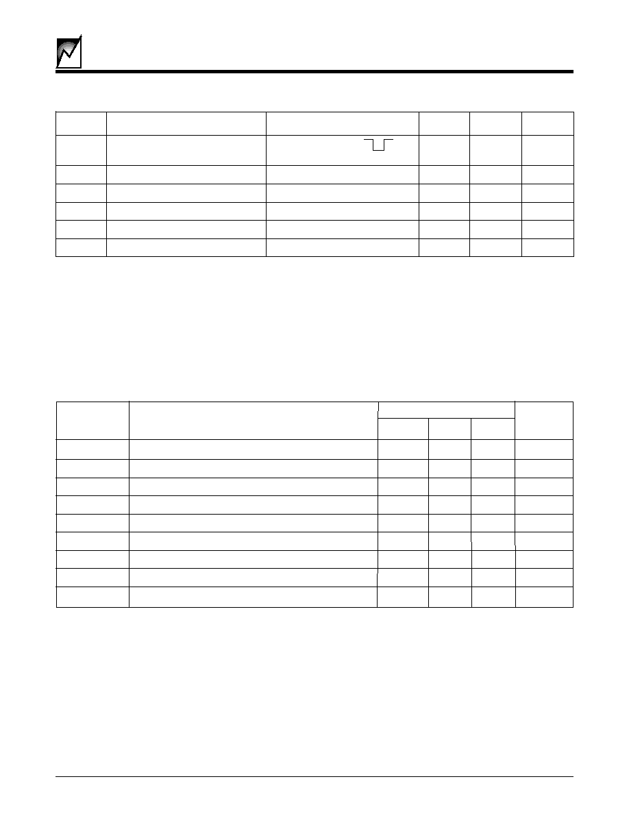
FIGURE 3. AUTOSTORE CYCLE TIMING DIAGRAM
STORE TIME
5
TIME (ms)
2017 ILL5.0
tASTO
VASEND
VASTH
VDD
V
O
L
TS (V)
AUTOSTORE CYCLE IN PROGRESS
Notes:
V
ASTH
= AUTOSTORE threshold voltage
V
ASEND
= AUTOSTORE cycle end voltage
t
ASTO
= AUTOSTORE cycle time
FIGURE 4. SLOW MODE TIMING
2017 ILL6.0
UP
VOUT
tDB
tGAP
1LSB Step
FIGURE 5. FAST MODE TIMING
2017 ILL7.0
tDB
tS FAST
tS SLOW
1 Second
VOUT
UP
1LSB Step
8
SMP9517
SUMMIT MICROELECTRONICS, Inc.
2035 3.0 5/10/00
NOTICE
SUMMIT Microelectronics, Inc. reserves the right to make changes to the products contained in this publication in order to improve
design, performance or reliability. SUMMIT Microelectronics, Inc. assumes no responsibility for the use of any circuits described
herein, conveys no license under any patent or other right, and makes no representation that the circuits are free of patent
infringement. Charts and schedules contained herein reflect representative operating parameters, and may vary depending upon
a user's specific application. While the information in this publication has been carefully checked, SUMMIT Microelectronics, Inc.
shall not be liable for any damages arising as a result of any error or omission.
SUMMIT Microelectronics, Inc. does not recommend the use of any of its products in life support applications where the failure or
malfunction of the product can reasonably be expected to cause failure of the life support system or to significantly affect its safety
or effectiveness. Products are not authorized for use in such applications unless SUMMIT Microelectronics, Inc. receives written
assurances, to its satisfaction, that: (a) the risk of injury or damage has been minimized; (b) the user assumes all such risks; and
(c) potential liability of SUMMIT Microelectronics, Inc. is adequately protected under the circumstances.
© Copyright 2000 SUMMIT Microelectronics, Inc.
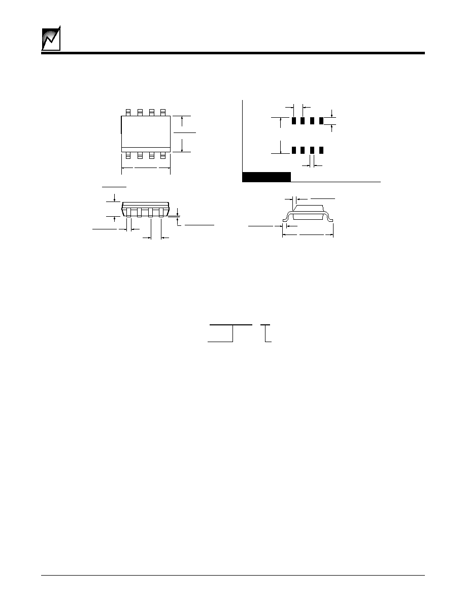
8 Pin SOIC (Type S) Package JEDEC (150 mil body width)
ORDERING INFORMATION
.228 (5.80)
.244 (6.20)
.016 (.40)
.035 (.90)
.020 (.50)
.010 (.25)
x45
∞
.0192 (.49)
.0138 (.35)
.061 (1.75)
.053 (1.35)
.0098 (.25)
.004 (.127)
.05 (1.27) TYP.
.275 (6.99) TYP.
.030 (.762) TYP.
8 Places
.050 (1.27) TYP.
.050 (1.270) TYP.
8 Places
.157 (4.00)
.150 (3.80)
.196 (5.00)
1
.189 (4.80)
FOOTPRINT
8pn JEDEC SOIC ILL.2
SMP9517
P
Base Part Number
Package
P = PDIP*
S = SOIC
*Special Order
2035 Tree 3.0