 | –≠–ª–µ–∫—Ç—Ä–æ–Ω–Ω—ã–π –∫–æ–º–ø–æ–Ω–µ–Ω—Ç: SMR100E | –°–∫–∞—á–∞—Ç—å:  PDF PDF  ZIP ZIP |
SMR100
T H I S P R O D U C T H A S R E A C H E D E N D O F L I F E
© SUMMIT Microelectronics, Inc.
2004 ∑ 1717 Fox Drive ∑ San Jose CA 95131 ∑ Phone 408 436-9890 ∑ FAX 408 436-9897
The Summit Web Site can be accessed by "right" or "left" mouse clicking on the link:
http://www.summitmicro.com/
2076 1.6 06/30/04
1
FEATURES & APPLICATIONS
∑ De-Bounced Reset Input with up to 40 Second
Programmable Delay Time
∑ External Push-Button Control Provides a
Reliable End-User System Reset Function
∑ Reset Signal at 3.0V with a Programmable
Timeout Period
∑ Brownout Warning Signal whenever the supply
dips below 3.1V
∑ Programmable Glitch Filtering of Brownout
Warning (BAD_PWR#) and Reset Function
∑ 8 Pin SOIC Package
∑ 6 ball Ultra CSP
TM
(Chip-Scale) Package
Applications
∑ Satellite and Cable-TV Set-top box
∑ Handheld PCs, Cameras, Camcorders, PDAs
∑ Security/Medical Alert Systems
INTRODUCTION
The SMR100 programmable reset controller is
designed for consumer applications specified by
Satellite-TV set-top box standards. The SMR100
provides a satellite box controller solution during initial
setup, changing programming cards and/or system
reset needs without removing power. The part can
accommodate a long-delay hold down of an external
reset push-button using an internal programmable de-
bounced timer. The part is factory programmed,
however, multiplexed programming pins are also
provided for in-system programming for prototype
purposes.
The required hold down time is programmable from
0.325 to 40 Sec with an internal on-chip oscillator.
Accurate warning of a 3.1V brownout condition
(BAD_PWR#), and a programmable reset
(RESET_OUT#) timeout period when the VDD supply
pin reaches 3.0V are also provided. During a reset
(RESET_OUT#), the part enables the "BAD_PWR#" or
brownout warning output until the reset has cleared. A
programmable glitch filter avoids nuisance tripping of
the internal comparators.
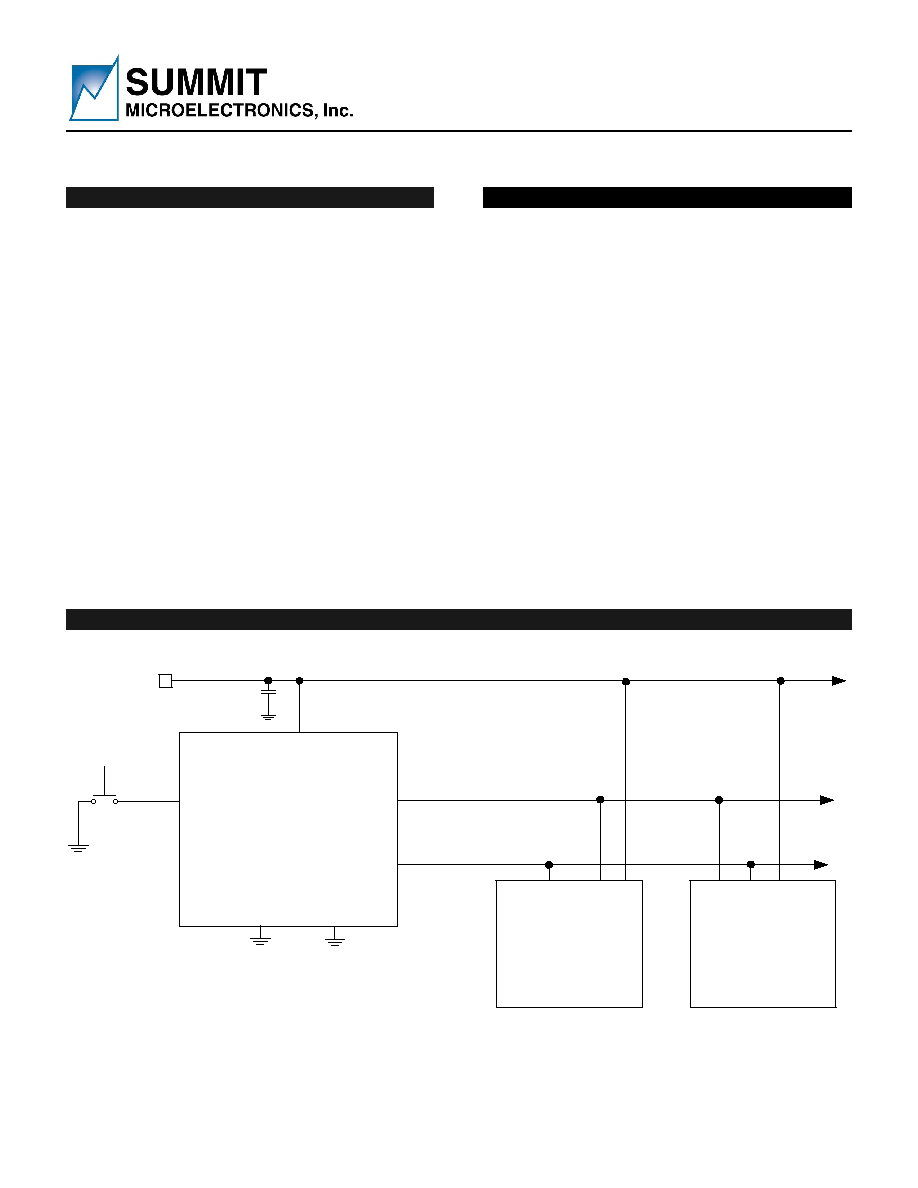
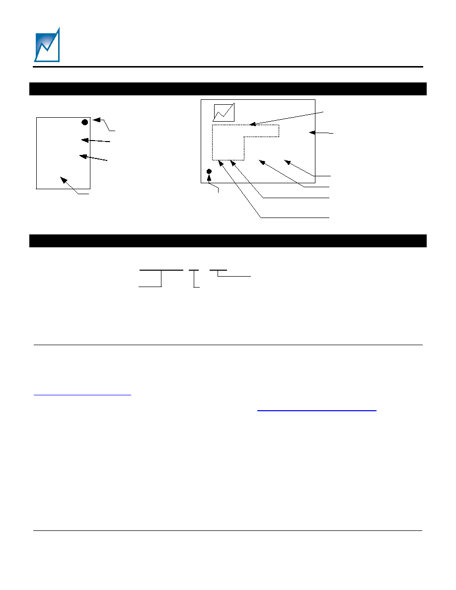
SIMPLIFIED APPLICATIONS DRAWING
FILT_CAP
TRIM_C
AP
SMR100
3.3V
3.3V
GN
D
VDD
PR
O
G
RESET_IN#
RESET_OUT#
BAD_PWR#
0.1
µf
ASIC
µP
Manual
Reset
Switch
Figure 1 ≠ Applications Schematic using the SMR100 to supervise the supply to digital components. As
shown, the SMR100 is designed to use a minimum of external components.
Programmable Long-Delay Push-Button Reset Controller for Consumer Equipment
SMR100
Preliminary Information
Summit Microelectronics, Inc
2076 1.6 06/30/04
2
GENERAL DESCRIPTION
The SMR100 is a programmable Reset Controller for
Consumer Equipment used to monitor the power
supply in µP and digital systems. It provides excellent
circuit reliability and low cost by eliminating external
components and adjustments when used with +3.3V
powered circuits. The device performs several
functions: it first asserts a `bad power' signal and then
a reset signal whenever the VDD supply voltage
declines below two preset thresholds, keeping it
asserted for a programmable time period after VDD
has risen above the reset threshold. The part also
provides a programmable delay push button input for
manual system reset.
The open-drain RESET_OUT# and BAD_PWR#
outputs have on-chip 100K pull-up resistors and do not
require external pull-up resistors unless more drive
current is needed (see figure 3). The RESET_OUT#
and BAD_PWR# comparators are designed to ignore
fast transients on VDD, and the outputs are
guaranteed to be in the correct logic state for VDD
down to 1V. Low supply current makes the SMR100
ideal for use in portable equipment. The RESET_IN#
input includes a programmable hold-down delay timer
for use with a push button switch for consumer
equipment such as set-top boxes and PCs.
A microprocessor's (µP's) reset input starts the µP in a
known state. The SMR100 asserts a reset to prevent
code -execution errors during power-up, power-down,
or UnderVoltage (UV) conditions. It asserts a
RESET_OUT# signal whenever the VDD supply
voltage declines below a 3.0V threshold, keeping it
asserted for a programmable period after VDD has
risen above the reset threshold. It also asserts a Bad
Power signal to warn of an impending reset or
brownout condition to allow time for the system to
save data before a reset occurs. The BAD_PWR#
signal is also asserted whenever RESET_OUT# is
asserted to prevent erroneous or false Bad Power
warnings during initial turn-on.
In addition to issuing a reset to the µP during power-
up, power-down, and brownout conditions, the
SMR100 is immune to short-duration VDD transients
(glitches) due to a programmable glitch filter. Typically,
a VDD transient of 100mV less than the reset
threshold and lasting for a duration less than the
programmed glitch filter setting will not cause a reset
pulse. A 0.1µF bypass capacitor mounted as close as
possible to the VDD pin provides additional transient
immunity. Since the BAD_PWR# and RESET_OUT#
outputs are open drain, the device interfaces easily
with µPs that have bidirectional-reset pins. Connecting
the RESET_OUT# output directly to the µP's RESET
pin allows either the µP or the SMR100 to assert a
reset.
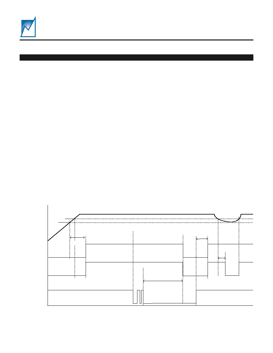
VDD
RESET_OUT#
BAD_PWR#
RESET_IN#
Push-Button
Input
T
RESET
T
RESET_HD
T
RESET
3.1V
3.0V
T
GLITCH
Push-Button
Released
Figure 2 ≠ SMR100 Operation and timing diagram
SMR100
Preliminary Information
Summit Microelectronics, Inc
2076 1.6 06/30/04
3
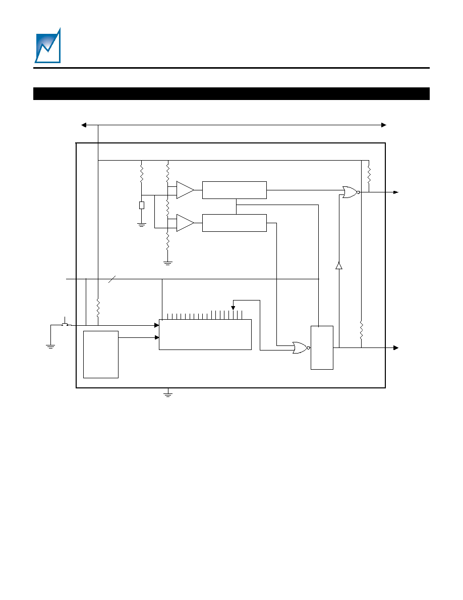
8 KHz
Ring
Oscillator,
+/-10%
accurate
Programmable Delay Generator/
Logic
Up Count
MSB
RESET_OUT
at 3.0V
Programmable
Hold-Down Time,
0.3125 to 40Sec
VDD
GND
User Reset
Pushbutton
-
-
+
+
1.25V
Vref
Programmable
Duration Glitch Filter
P
r
ogra
mmable
Dura
tion Re
se
t
Ou
tput
Reset
User Reset
Programmable
Duration Glitch Filter
RESET _IN#
RESET_OUT#
BAD_PWR#
3.3V
BAD_PWR
at 3.1V
100k
100k
100k
PROG
2
Figure 3 ≠ SMR100 Controller Internal Block Diagram.
INTERNAL BLOCK DIAGRAM
SMR100
Preliminary Information
Summit Microelectronics, Inc
2076 1.6 06/30/04
4
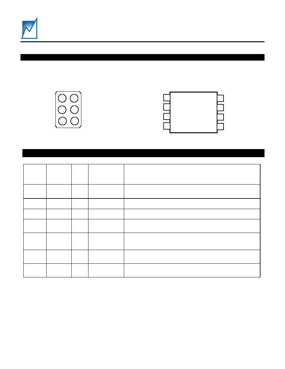
PACKAGE AND PIN CONFIGURATION
RESET_IN#
VDD
RESET_OUT#
GND
PROG
A1 A2
B1
B2
C1 C2
BAD_PWR#
1
2
4
3
8
7
5
6
PROG
NC
RESET_IN#
GND
VDD
NC
BAD_PWR#
RESET_OUT#
PIN DESCRIPTIONS
CSP
Pin
Number
SOIC
Pin
Number
Pin
Type
Pin Name
Pin Description
A1
1 I
PROG
High voltage programming pin. Set to 12V in programming
mode. Connected to ground if not used.
A2
8 PWR
VDD
Positive supply voltage.
B1
4 PWR
GND
Ground pin.
B2
5 O
RESET_OUT# Open Drain active low Reset Out indicator. Internally connected
to VDD through a 100K
resistor.
C1
3 I
RESET_IN#
De-bounced push button switch input. Internally connected to
VDD through a 100K
resistor. Also used as the Data input
programming pin when the PROG pin is set to 12V.
C2
6 O
BAD_PWR#
Open Drain active low Bad Power indicator. Internally
connected to VDD through a 100K
resistor.
NA
2,7 NC
NC
No Connect
6 Ball Ultra CSP
TM
Bottom View
8 Pin SOIC
Top View
SMR100
Preliminary Information
Summit Microelectronics, Inc
2076 1.6 06/30/04
5
ABSOLUTE MAXIMUM RATINGS
Temperature Under Bias ......................-55
∞
C to 125
∞
C
Storage Temperature............................-65
∞
C to 125
∞
C
Terminal Voltage with Respect to GND:
V
DD
........................................-0.3V to 6.0V
PROG, RESET_IN#................-0.3V to 16.0V
All Others.................................VDD + 0.7V
Output Short Circuit Current .................. 100mA
Reflow Solder Temperature (30 secs)................ 240
∞
C
ESD Rating per JEDEC.................................2000V
Latch-Up testing per JEDEC........................
±100mA
Note - The device is not guaranteed to function outside its operating
rating. Stresses listed under Absolute Maximum Ratings may cause
permanent damage to the device. These are stress ratings only and
functional operation of the device at these or any other conditions
outside those listed in the operational sections of the specification is
not implied. Exposure to any absolute maximum rating for extended
periods may affect device performance and reliability. Devices are
ESD sensitive. Handling precautions are recommended.
RECOMMENDED OPERATING CONDITIONS
Temperature Range (Commercial)..........≠5
∞
C to +70
∞
C
Supply Voltage......................................3.3V +/-10%
1
Programming Supply Voltage..................12.0V +/-10%
Note 1 ≠ The device can operate over a supply range of
2.7V to 5.5V.
Package Thermal Resistance (
JA
)
8 Pin SOIC................................................23
o
C/W
6 Ball Ultra
CSP
TM
....................................TBD
o
C/W
Moisture Classification Level 1 (MSL 1) per J-STD- 020
RELIABILITY CHARACTERISTICS
Data Retention........................................100 Years
Endurance......................................100,000 Cycles
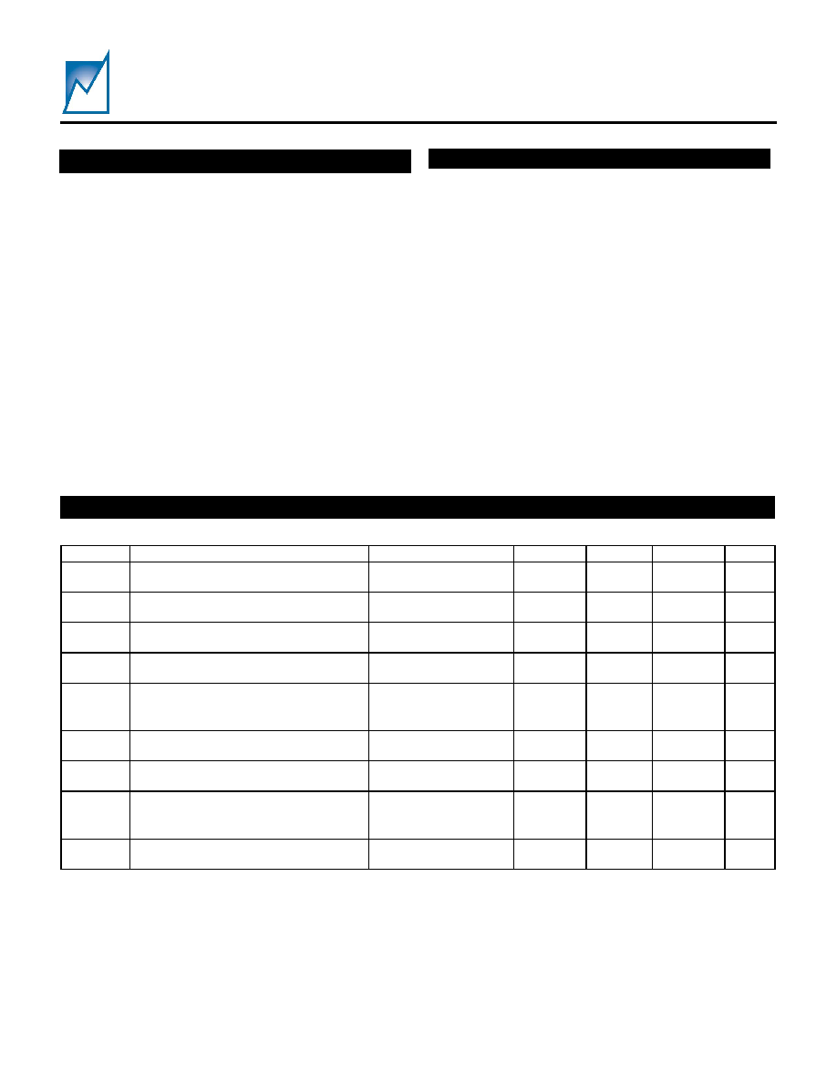
DC OPERATING CHARACTERISTICS
(Over recommended operating conditions, unless otherwise noted. All voltages are relative to GND.)
Symbol Parameter
Notes
Min.
Typ.
Max
Unit
V
DD
Supply Voltage Range
2.7
3.3
5.5
V
V
PROG
Programming Supply Voltage Range
10.0
12.0
15.0
V
V
RT
Reset
Threshold
2.95
3.0 3.05 V
V
BPT
Bad Power Warning Threshold
3.05
3.1
3.15
V
I
DD
Power Supply Current
VDD = 3.3V, no
RESET_OUT# in
progress
100
200
µA
V
IH
Input High Voltage
VDD = 3.3V 0.9xVDD
VDD
V
V
IL
Input Low Voltage
VDD = 3.3V
0.1xVDD
V
V
OL
Programmable Active High or Low
Open Drain Outputs (RESET_OUT#,
BAD_PWR#)
ISINK = 1mA
0
0.4
V
I
OL
Output Low Current
0 1.0
mA
SMR100
Preliminary Information
Summit Microelectronics, Inc
2076 1.6 06/30/04
6
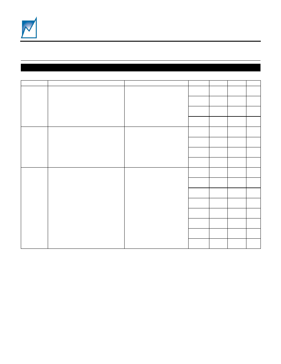
AC OPERATING CHARACTERISTICS
(Over recommended operating conditions, unless otherwise noted. All voltages are relative to GND.)
Symbol Parameter
Notes Min.
Typ.
Max
Unit
0.8 1 1.2
ms
20 25 30
ms
80 100 120
ms
T
RESET_OUT
Reset Timeout period
Programmed Default = 25ms
160 200 240 ms
3 4 5
µs
4.5 6 7.5
µs
7.5 10 12.5
µs
t
GLITCH
Programmable glitch filter times
Programmed Default = 4
µs
13.5 18 22.5
µs
0.26 0.325 0.39 s
0.5 0.625 0.75 s
1 1.25
1.5 s
2 2.5 3 s
4 5 6
s
8 10 12
s
16 20 24 s
t
RESET_HD
Programmable Reset Hold-Down
Delay times
Programmed Default = 10s
32 40 48 s
SMR100
Preliminary Information
Summit Microelectronics, Inc
2076 1.6 06/30/04
7
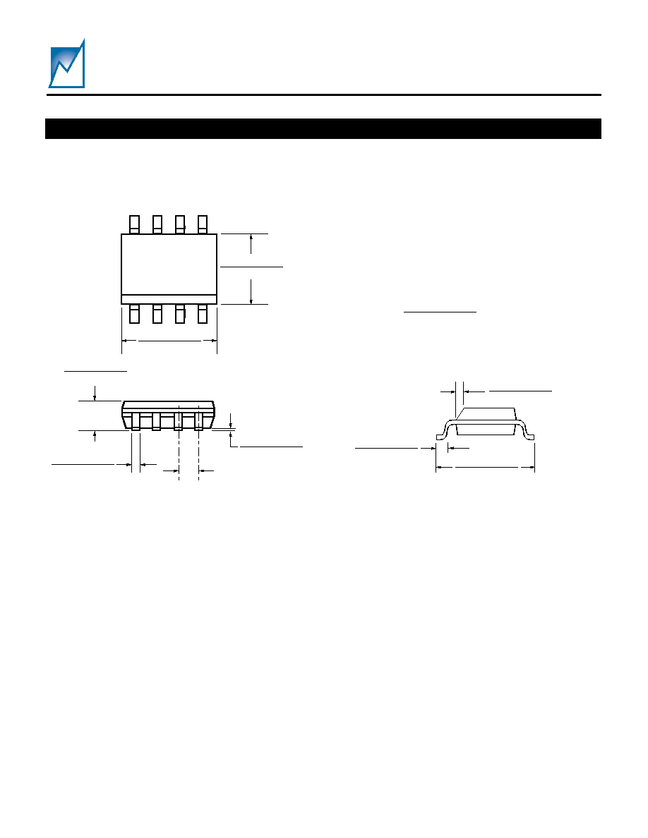
8 Pin SOIC Package
.05 (1.27) TYP.
1
8 Pin SOIC
0.150 - 0.157
(3.80 - 4.00)
0.189 - 0.196
(4.80 - 5.00)
0.053 - 0.069
(1.35 - 1.75)
0.013 - 0.020
(0.33 - 0.51)
0.004 - 0.010
(0.10 - 0.25)
0.016 - 0.050
(0.40 - 1.27)
◊45∫
0.010 - 0.020
(0.25 - 0.50)
0.228 - 0.244
(5.80 - 6.20)
Ref. JEDEC MS-012
Inches
(Millimeters)
PACKAGE OUTLINE
SMR100
Preliminary Information
Summit Microelectronics, Inc
2076 1.6 06/30/04
8
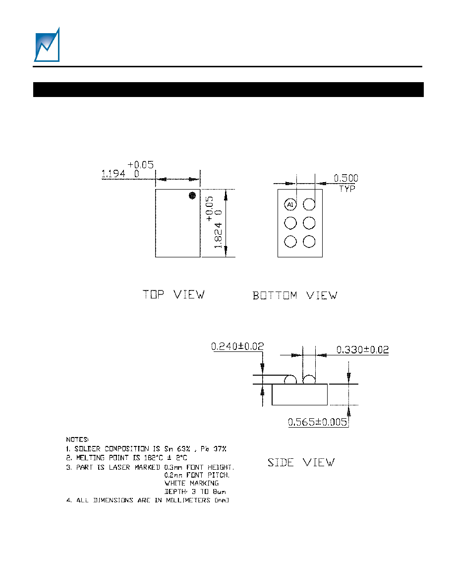
6 Ball Ultra CSP
TM
≠ Chip Scale Package
PACKAGE OUTLINE (CONTINUED)
SMR100
Preliminary Information
Summit Microelectronics, Inc
2076 1.6 06/30/04
9
PART MARKING
SMR100S
AYYWW
Pin 1
Identifier
Annn
Summit Part Number
Date Code (YYWW)
Part Number suffix
(Contains Customer specific
ordering requirements)
Lot tracking code (Summit use)
Drawing
not to scale
xx
Status Tracking Code
(Blank, MS, ES, 01, 02,...)
(Summit Use)
Product Tracking Code
(Summit use)
SUMMIT
ORDERING INFORMATION
The default device ordering number is SMR100E-100 and is programmed as described in the AC Operating
Characteristics table on page 6 and tested over the commercial temperature range.
NOTICE
NOTE 1 - This is a Preliminary Information data sheet that describes a Summit product currently in pre-production with limited characterization.
Revision 1.6 - This document supersedes all previous versions. Data Sheet updates can be accessed by "right" or "left" mouse clicking on the link:
http://www.summitmicro.com/
Device Errata sheets can be accessed by "right" or "left" mouse clicking on the link:
http://www.summitmicro.com/errata/
SUMMIT Microelectronics, Inc. reserves the right to make changes to the products contained in this publication in order to improve design,
performance or reliability. SUMMIT Microelectronics, Inc. assumes no responsibility for the use of any circuits described herein, conveys no license
under any patent or other right, and makes no representation that the circuits are free of patent infringement. Charts and schedules contained
herein reflect representative operating parameters, and may vary depending upon a user's specific application. While the information in this
publication has been carefully checked, SUMMIT Microelectronics, Inc. shall not be liable for any damages arising as a result of any error or
omission.
SUMMIT Microelectronics, Inc. does not recommend the use of any of its products in life support or aviation applications where the failure or
malfunction of the product can reasonably be expected to cause any failure of either system or to significantly affect their safety or effectiveness.
Products are not authorized for use in such applications unless SUMMIT Microelectronics, Inc. receives written assurances, to its satisfaction, that:
(a) the risk of injury or damage has been minimized; (b) the user assumes all such risks; and (c) potential liability of SUMMIT Microelectronics, Inc.
is adequately protected under the circumstances.
© Copyright 2004 SUMMIT MICROELECTRONICS, Inc.
Programmable Analog for a Digital WorldTM
Ultra CSP
TM
is a registered name of FlipChip International, LLC.
SMR100
E
Package
E = 6 Ball Ultra CSP
TM
Summit Part Number
nnn
Part Number Suffix
Customer specific requirements are contained
in the suffix such as Hex code, Hex code
revision, etc.
S = 8 Pin SOIC
An
nn
SSYWW
Ball A1
Identifier
Part Number suffix-nnn
(Customer specific
ordering requirements)
Date Code
Y = Single digit year
(4=2004, 5=2005, etc)
Drawing
not to scale
Product Tracking
Code (Summit use)