 | –≠–ª–µ–∫—Ç—Ä–æ–Ω–Ω—ã–π –∫–æ–º–ø–æ–Ω–µ–Ω—Ç: SMS2916SA | –°–∫–∞—á–∞—Ç—å:  PDF PDF  ZIP ZIP |
SUMMIT MICROELECTRONICS, Inc. ∑ 300 Orchard City Drive, Suite 131 ∑ Campbell, CA 95008 ∑ Telephone 408-378-6461 ∑ Fax 408-378-6586 ∑ www.summitmicro.com
1
© SUMMIT MICROELECTRONICS, Inc. 2000
2028 5.1 8/2/00
Characteristics subject to change without notice
SUMMIT
MICROELECTRONICS, Inc.
FEATURES
∑
Precision Voltage Monitor
≠ V
CC
Supply Monitor
- Complementary reset outputs for complex
microcontroller systems
- Integrated memory write lockout function
- No external components required
∑Watchdog Timer
≠ 1600 ms, internal
∑
Two Wire Serial Interface (I
2
CTM)
∑
Extended Programmable Functions
available on SMS24
∑
High Reliability
≠ Endurance: 100,000 erase/write cycles
≠ Data retention: 100 years
∑ 8-Pin SOIC Packages
Voltage Supervisory Circuit With Watchdog Timer
SMS2902/SMS2904/SMS2916
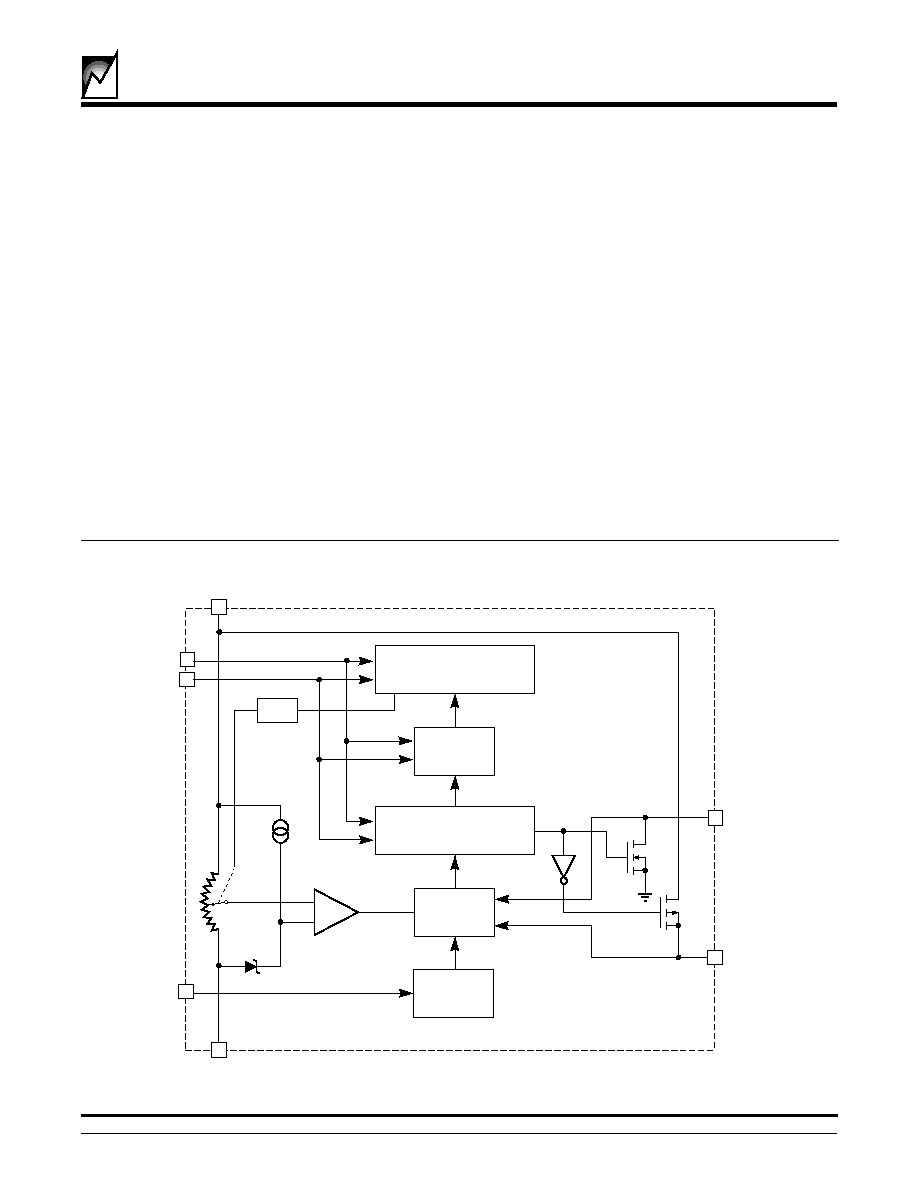
OVERVIEW
The SMS29xx is a power supervisory circuit that monitors
V
CC
and will generate complementary reset outputs. The
reset pins also act as I/Os and may be used for signal
conditioning. The SMS29xx also has an on-board watch-
dog timer.
The SMS29xx integrates a nonvolatile serial memory. It
features the industry standard I
2
C serial
interface allowing quick implementation in an end-users'
system.
BLOCK DIAGRAM
+
≠
GND
VCC
8
4
RESET#
2
VTRIP
RESET
CONTROL
RESET
7
1.26V
SCL
6
SDA
5
WATCHDOG
TIMER
WDI#
1
2028 T BD 2.0
WRITE
CONTROL
NONVOLATILE
MEMORY
ARRAY
PROGRAMMABLE
RESET PULSE
GENERATOR
2
SMS2902/SMS2904/SMS2916
2028 5.1 8/2/00
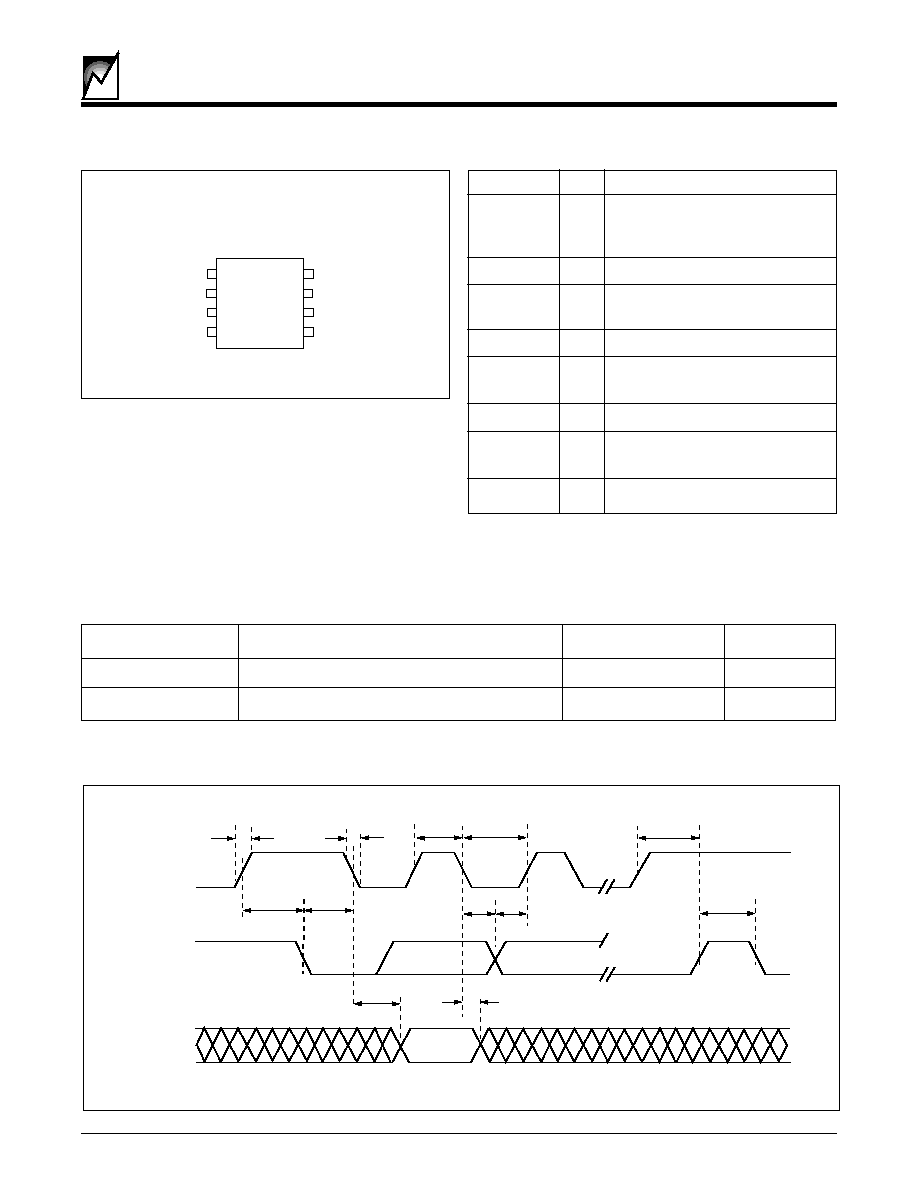
PIN CONFIGURATIONS
PIN NAMES
Symbol
Pin
Description
WDI#
1
Watchdog Input /a high to
low transition will clear the
watchdog timer
RESET#
2
Active Low RESET Input/Output
NC
3
No Connect, tie to ground
or leave open
GND
4
Analog and Digital Ground
SDA
5
Serial Memory Input/
Output data line
SCL
6
Serial Memory clock input
RESET
7
Active High RESET Input/
Output
V
CC
8
Supply Voltage
2028 PGM T1.1
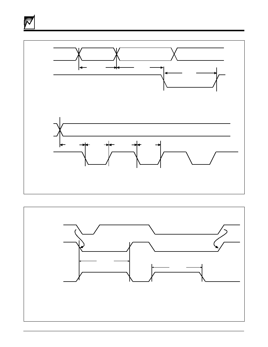
FIGURE 1. SERIAL BUS TIMING DIAGRAM
CAPACITANCE
T
A
= 25∞C, f = 100KHz
Symbol
Parameter
Max
Units
C
IN
Input Capacitance
5
pF
L
OUT
Output Capacitance
8
pF
2028 PGM T2..0
SCL
SDA In
SDA Out
t
AA
t
R
t
H IGH
t
LOW
t
SU:STO
t
BUF
t
SU:DAT
t
HD:DAT
t
HD:SDA
t
SU:SDA
t
DH
2028 ILL5.0
t
F
WDI#
RESET#
NC
GND
VCC
RESET
SCL
SDA
1
2
3
4
8
7
6
5
8-Pin SOIC
2028 T PCon 2.0
SMS2902/SMS2904/SMS2916
3
2028 5.1 8/2/00
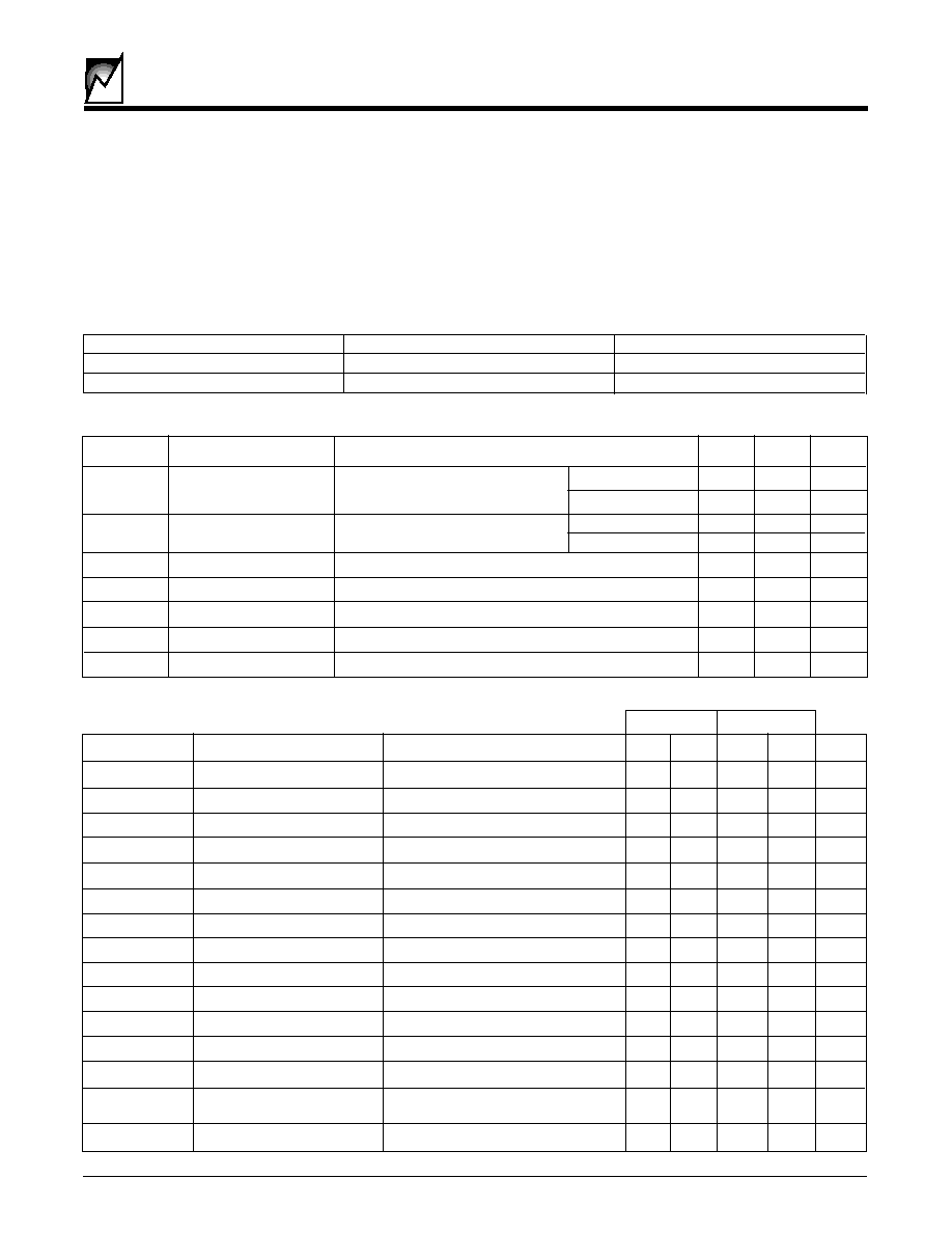
ABSOLUTE MAXIMUM RATINGS
Temperature Under Bias
............................................................................................................................... -40∞C to +85∞C
Storage Temperature
..................................................................................................................................... -65∞C to +125∞C
Soldering Temperature (less than 10 seconds) ................................................................................................................... 300∞C
Supply Voltage
............................................................................................................................................................. 0 to 6.5V
Voltage on Any Pin
....................................................................................................................................... -0.3V to V
CC
+0.3V
ESD Voltage (JEDEC method) .......................................................................................................................................... 2,000V
NOTE: These are STRESS ratings only. Appropriate conditions for operating these devices are given elsewhere in this specification. Stresses
beyond those listed here may permanently damage the part. Prolonged exposure to maximum ratings may affect device reliability.
2.7V to 4.5V
4.5V to 5.5V
Symbol
Parameter
Conditions
Min
Max
Min
Max
Units
f
SCL
SCL Clock Frequency
0
100
400
KHz
t
LOW
Clock Low Period
4.7
1.3
µs
t
HIGH
Clock High Period
4.0
0.6
µs
t
BUF
Bus Free Time
Before New Transmission
4.7
1.3
µs
t
SU:STA
Start Condition Setup Time
4.7
0.6
µs
t
HD:STA
Start Condition Hold Time
4.0
0.6
µs
t
SU:STO
Stop Condition Setup Time
4.7
0.6
µs
t
AA
Clock to Output
SCL Low to SDA Data Out Valid
0.3
3.5
0.2
0.9
µs
t
DH
Data Out Hold Time
SCL Low to SDA Data Out Change
0.3
0.2
µs
t
R
SCL and SDA Rise Time
1000
300
ns
t
F
SCL and SDA Fall Time
300
300
ns
t
SU:DAT
Data In Setup Time
250
100
ns
t
HD:DAT
Data In Hold Time
0
0
ns
T
I
Noise Spike Width
Noise Suppression Time Constant
100
100
ns
@ SCL, SDA Inputs
t
WR
Write Cycle Time
10
10
ms
AC ELECTRICAL CHARACTERISTICS
(over recommended operating conditions unless otherwise specified)
2028 PGM T5.0
2028 PGM T4.0
DC ELECTRICAL CHARACTERISTICS (over recommended operating conditions unless otherwise specified)
Symbol
Parameter
Conditions
Min
Max
Units
SCL = CMOS Levels @ 100KHz
V
CC
=5.5V
3
mA
I
CC
Supply Current (CMOS)
SDA = Open
All other inputs = GND or V
CC
V
CC
=3.3V
2
mA
I
SB
Standby Current (CMOS)
SCL = SDA = V
CC
V
CC
=5.5V
50
µA
All other inputs = GND
I
LI
Input Leakage
V
IN
= 0 To V
CC
10
µA
I
LO
Output Leakage
V
OUT
= 0 To V
CC
10
µA
V
IL
Input Low Voltage
S0, S1, S2, SCL, SDA, RESET#
0.3xV
CC
V
V
IH
Input High Voltage
S0, S1, S2, SCL, SDA, RESET
0.7xV
CC
V
V
OL
Output Low Voltage
I
OL
= 3mA SDA
0.4
V
V
CC
=3.3V
25
µA
Temperature
Min
Max
Commercial
0∞C
+70∞C
Industrial
-40∞C
+85∞C
RECOMMENDED OPERATING CONDITIONS
2028 PGM T3.0
4
SMS2902/SMS2904/SMS2916
2028 5.1 8/2/00
FIGURE 2. RESET OUTPUT TIMING
RESET CIRCUIT AC and DC ELECTRICAL CHARACTERISTICS
TA=-40∞C to +85∞C
Symbol
Parameter
Part no.
Min.
Typ.
Max.
Unit
Suffix
V
TRIP
Reset Trip Point
A (or) Blank
4.250
4.375
4.5
V
B
4.50
4.625
4.75
V
2.7
2.55
2.65
2.75
V
t
PURST
Reset Timeout
200
ms
t
RPD
V
TRIP
to RESET Output Delay
5
µs
V
RVALID
RESET Output Valid to V
CC
min. Guarantee
1
V
t
GLITCH
Glitch Reject Pulse Width note 1
30
ns
V
OLRS
RESET Output Low Voltage I
OL
= 1mA
0.4
V
V
OHRS
RESET High Voltage Output I
OH
= 800µA
V
CC
-.75
V
V
ULH
V
SENSE
Under-voltage threshold low to high
1.20
1.25
1.30
V
V
UHL
V
SENSE
Under-voltage threshold high to low
1.20
1.25
1.30
V
V
OLH
V
SENSE
Over-voltage threshold low to high
1.20
1.25
1.30
V
V
OHL
V
SENSE
Over-voltage threshold high to low
1.20
1.25
1.30
V
t
VD1
Delay to V
LOW
Active
5
µs
t
VD2
Delay to V
LOW
Released
5
µs
t
WDTO
Watchdog timeout Period
1600
ms
VCC
VRVALID
VTRIP
tPURST
RESET#
RESET
2028 T fig02 2.0
tGLITCH
tRPD
tPURST
tRPD
SMS2902/SMS2904/SMS2916
5
2028 5.1 8/2/00
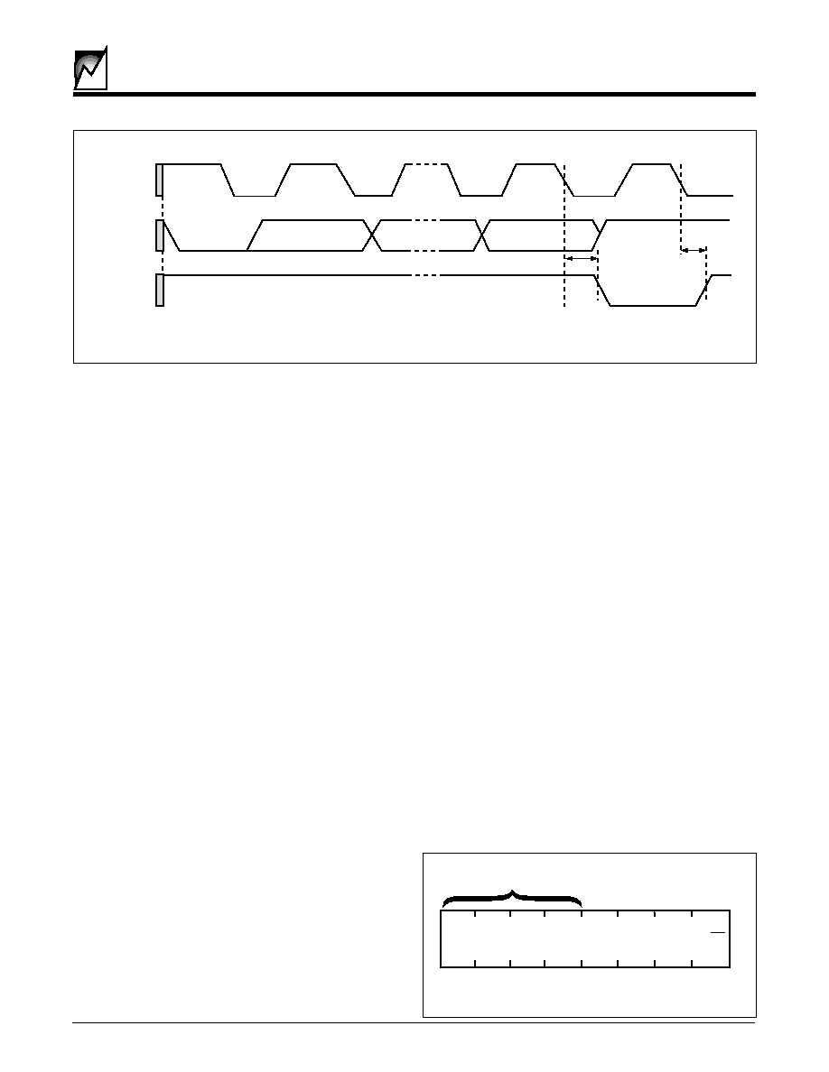
FIGURE 3. WATCHDOG TIMER TIMING DIAGRAM
FIGURE 4.
RESET
RESET
RESET
RESET
RESET
AS AN INPUT FUNCTION
t
PURST
t
PURST
RESET (out)
2028 T fig04 2.0
RESET# (in)
RESET# (out)
t
WDTO
t
PURST
t
WDTO
t
PURST
t
PURST
t
WDTO
< t
WDTO
2028 T fig03 2.0
RESET#
RESET#
WDI#
WDI#

6
SMS2902/SMS2904/SMS2916
2028 5.1 8/2/00
ENDURANCE AND DATA RETENTION
The SMS29xx is designed for applications requiring
100,000 erase/write cycles and unlimited read cycles. It
provides 100 years of secure data retention, with or
without power applied, after the execution of 100,000
erase/write cycles.
Reset Controller Description
The SMS29xx provides a precision RESET controller
that ensures correct system operation during brown-out
and power-up/-down conditions. It is configured with two
open drain RESET outputs; pin 7 is an active high output
and pin 2 is an active low output.
During power-up, the RESET outputs remain active until
V
CC
reaches the V
TRIP
threshold and will continue driving
the outputs for t
PURST
(200 msec) after reaching V
TRIP
.
The RESET outputs will be valid so long as V
CC
is > 1.0V.
During power-down, the RESET outputs will begin driv-
ing active when V
CC
falls below V
TRIP
.
The RESET pins are I/Os; therefore, the SMS29xx can
act as a signal conditioning circuit for an externally
applied reset. The inputs are edge triggered; that is, the
RESET input will initiate a reset timeout after detecting a
low to high transition and the RESET# input will initiate a
reset timeout after detecting a high to low transition. Refer
to the applications Information section for more details on
device operation as a reset conditioning circuit.
WATCHDOG TIMER OPERATION
The SMS29xx has a watchdog timer with a program-
mable timeout period. Whenever the watchdog times out
it will generate a reset output on both RESET# and
RESET.
Any transition on WDI will clear the watchdog timer. If a
transition is not detected within t
WDTO
seconds the watch-
dog will time out and force the reset outputs active.
PIN DESCRIPTIONS
Serial Clock (SCL) - The SCL input is used to clock data
into and out of the device. In the WRITE mode, data must
remain stable while SCL is HIGH. In the READ mode, data
is clocked out on the falling edge of SCL.
Serial Data (SDA) - The SDA pin is a bidirectional pin
used to transfer data into and out of the device. Data may
change only when SCL is LOW, except START and STOP
conditions. It is an open-drain output and may be wire-
ORed with any number of open-drain or open-collector
outputs.
RESET# - RESET# is an active low output. Whenever V
CC
is below V
TRIP
the SMS29xx will drive the RESET# pin to
ground. The RESET# pin is an I/O and can be used as a
reset input. Refer to Figure 1 as an example use of this pin
as a push button switch debounce circuit. It should be
noted this is an open drain output and an external pull-up
resistor tied to V
CC
is needed for proper operation.
RESET -- RESET is an active high output. Whenever V
CC
is below V
TRIP
the SMS29xx will drive the RESET pin to the
V
CC
rail. The RESET pin is an I/O and can be used as a
reset input. It should be noted this is an open drain output
and an external pull-down resistor tied to ground is needed
for proper operation.
WDI# - The WDI# input is used as a hardware method of
clearing the watchdog timer. A high to low transition on this
pin will clear the watchdog timer. If a transition is not
detected within 1.6 seconds the watchdog will time out
and force the reset outputs active.
SMS2902/SMS2904/SMS2916
7
2028 5.1 8/2/00
FIGURE 5. ACKNOWLEDGE RESPONSE FROM RECEIVER
CHARACTERISTICS OF THE I
2
C BUS
General Description
The I
2
C bus was designed for two-way, two-line serial
communication between different integrated circuits. The
two lines are: a serial data line (SDA), and a serial clock
line (SCL). The SDA line must be connected to a positive
supply by a pull-up resistor, located somewhere on the
bus (See Figure 1). Data transfer between devices may
be initiated with a START condition only when SCL and
SDA are HIGH (bus is not busy).
Input Data Protocol
One data bit is transferred during each clock pulse. The
data on the SDA line must remain stable during clock
HIGH time, because changes on the data line while SCL
is HIGH will be interpreted as start or stop condition.
START and STOP Conditions
When both the data and clock lines are HIGH, the bus is
said to be not busy. A HIGH-to-LOW transition on the data
line, while the clock is HIGH, is defined as the "START"
condition. A LOW-to-HIGH transition on the data line,
while the clock is HIGH, is defined as the "STOP" condi-
tion .
DEVICE OPERATION
The SMS29xx is a 2K/4K/16K serial E
2
PROM. The de-
vice supports the I
2
C bidirectional data transmission
protocol. The protocol defines any device that sends data
onto the bus as a "transmitter" and any device which
receives data as a "receiver." The device controlling data
transmission is called the "master" and the controlled
device is called the "slave." In all cases, the SMS29xx will
be a "slave" device, since it never initiates any data
transfers.
FIGURE 6. SLAVE ADDRESS BYTE
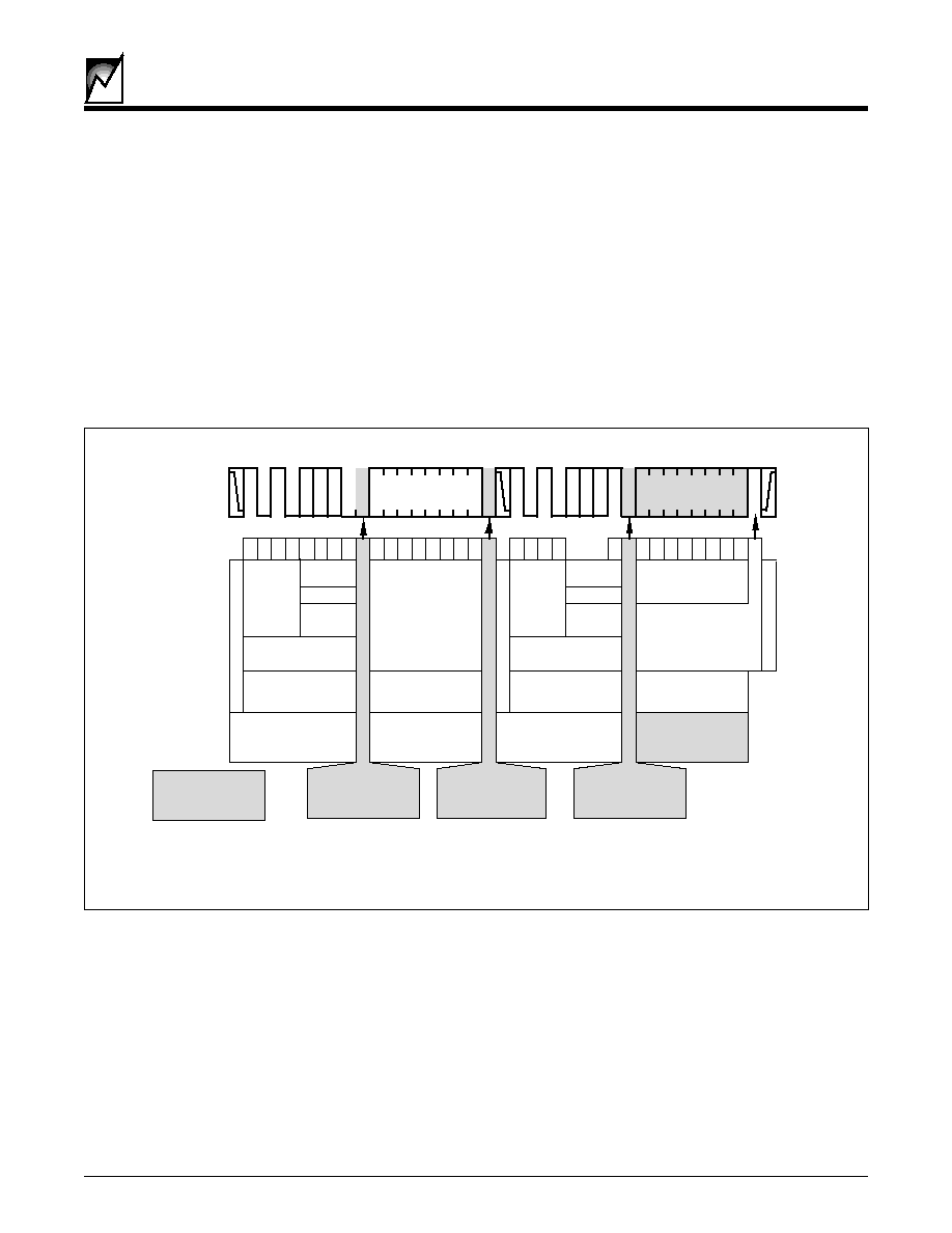
Acknowledge (ACK)
Acknowledge is a software convention used to indicate
successful data transfers. The transmitting device, either
the master or the slave, will release the bus after transmit-
ting eight bits. During the ninth clock cycle, the receiver
will pull the SDA line LOW to ACKnowledge that it re-
ceived the eight bits of data (See Figure 5).
The SMS29xx will respond with an ACKnowledge after
recognition of a START condition and its slave address
byte. If both the device and a write operation are selected,
the SMS29xx will respond with an ACKnowledge after the
receipt of each subsequent 8-bit word.
In the READ mode, the SMS29xx transmits eight bits of
data, then releases the SDA line, and monitors the line for
an ACKnowledge signal. If an ACKnowledge is detected,
and no STOP condition is generated by the master, the
SMS29xx will continue to transmit data. If an
ACKnowledge is not detected, the SMS29xx will terminate
further data transmissions and awaits a STOP condition
before returning to the standby power mode.
Device Addressing
Following a start condition the master must output the
address of the slave it is accessing. The most significant
four bits of the slave address are the device type identifier
(`1010') (see figure 6).
SCL from
Master
Data Output
from
Transmitter
Data Output
from
Receiver
Start
Condition
ACKnowledge
t
AA
t
AA
1
8
9
2028 ILL7.0
1 0 1 0
R/W
DEVICE
IDENTIFIER
2028 ILL8.1
A
10
*
A
8
**
A
9
*
* = 2916 only
** = 2904 only
8
SMS2902/SMS2904/SMS2916
2028 5.1 8/2/00
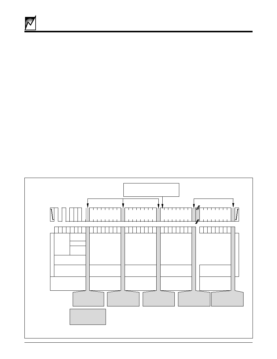
FIGURE 7. PAGE/BYTE WRITE MODE
WRITE OPERATIONS
The SMS29xx allows two types of write operations: byte
write and page write. The byte write operation writes a
single byte during the nonvolatile write period (t
WR
). The
page write operation allows up to 16 bytes in the same
page to be written during t
WR
.
Byte WRITE
Upon receipt of both the slave address and word address,
the SMS29xx responds with an ACKnowledge for each.
After receiving the next byte of data, it again responds with
an ACKnowledge. The master then terminates the trans-
fer by generating a STOP condition, at which time the
SMS29xx begins the internal write cycle.
While the internal write cycle is in progress, the SMS29xx
inputs are disabled, and the device will not respond to any
requests from the master. Refer to Figure 7 for the
address, ACKnowledge and data transfer sequence.
Page WRITE
The SMS29xx is capable of a 16-byte page write opera-
tion. It is initiated in the same manner as the byte-write
operation, but instead of terminating the write cycle after
the first data word, the master can transmit up to 15 more
bytes of data. After the receipt of each byte, the SMS29xx
will respond with an ACKnowledge.
The SMS29xx automatically increments the address for
subsequent data words. After the receipt of each word,
the low order address bits are internally incremented by
one. The high order five bits of the address byte remain
constant. Should the master transmit more than 16 bytes,
prior to generating the STOP condition, the address
counter will "roll over," and the previously written data will
be overwritten. As with the byte-write operation, all inputs
are disabled during the internal write cycle. Refer to
Figure 7 for the address, ACKnowledge and data transfer
sequence.
The next three bits are the high order address bits on the
2904 and 2916 and are "Don't Care" on the 2902.
Read/Write Bit
The last bit of the data stream defines the operation to be
performed. When set to "1," a read operation is selected;
when set to "0," a write operation is selected.
D
7
D
6
D
5
D
4
D
3
D
2
D
1
D
0
D
7
D
6
D
5
D
4
D
3
D
2
D
1
D
0
A
7
A
6
A
5
A
4
A
3
A
2
A
1
A
0
D
7
D
5
D
6
D
4
D
0
D
3
D
2
D
1
S
T
A
R
T
Word Address
Data Byte n
Data Byte n+15
S
T
O
P
A
C
K
Acknowledges Transmitted from
SMS29xx to Master Receiver
Slave Address
Device
Type
Address
Read/Write
0= Write
SDA
Bus
Activity
A
C
K
A
C
K
Master Sends Read
Request to Slave
Master Writes Word
Address to Slave
1 0 1 0
0
Data Byte n+1
A
C
K
Master Writes
Data to Slave
Master Transmitter
to
Slave Receiver
Slave Transmitter
to
Master Receiver
Slave Transmitter
to
Master Receiver
Master Transmitter
to
Slave Receiver
Master Transmitter
to
Slave Receiver
Shading Denotes
SMS29xx
SDA Output Active
Master Transmitter
to
Slave Receiver
Slave Transmitter
to
Master Receiver
Slave Transmitter
to
Master Receiver
Master Transmitter
to
Slave Receiver
Slave Transmitter
to
Master Receiver
Master Writes
Data to Slave
Master Writes
Data to Slave
Acknowledges Transmitted from
SMS29xx to Master Receiver
If single byte-write only,
Stop bit issued here.
X
X
R
W
A
10
A
9
A
10
A
9
A
C
K
2028 ILL9.1
SMS2902/SMS2904/SMS2916
9
2028 5.1 8/2/00
FIGURE 9. CURRENT ADDRESS BYTE READ MODE
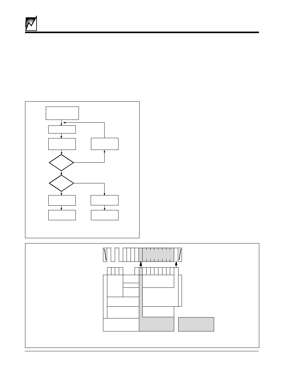
FIGURE 8. ACKNOWLEDGE POLLING
Acknowledge Polling
When the SMS29xx is performing an internal WRITE
operation, it will ignore any new START conditions. Since
the device will only return an acknowledge after it accepts
the START, the part can be continuously queried until an
acknowledge is issued, indicating that the internal WRITE
cycle is complete.
To poll the device, give it a START condition, followed by
a slave address for a WRITE operation (See Figure 8).
READ OPERATIONS
Read operations are initiated with the R/W bit of the
identification field set to "1." There are four different read
options:
1.
Current Address Byte Read
2.
Random Address Byte Read
3.
Current Address Sequential Read
4.
Random Address Sequential Read
Current Address Byte Read
The SMS29xx contains an internal address counter which
maintains the address of the last word accessed,
incremented by one. If the last address accessed (either
a read or write) was to address location n, the next read
operation would access data from address location n+1
and increment the current address pointer. When the
SMS29xx receives the slave address field with the R/W bit
set to "1," it issues an acknowledge and transmits the 8-
bit word stored at address location n+1.
The current address byte read operation only accesses a
single byte of data. The master does not acknowledge the
transfer, but does generate a stop condition. At this point,
the SMS29xx discontinues data transmission. See Figure
9 for the address acknowledge and data transfer se-
quence.
Issue Start
Internal WRITE Cycle
In Progress;
Begin ACK Polling
Issue Slave
Address and
R/W = 0
ACK
Returned?
Next
operation a
WRITE?
Issue Byte
Address
Proceed with
WRITE
Issue Stop
Await Next
Command
Issue Stop
No
No
Yes (Internal WRITE Cycle is completed)
Yes
2028 ILL10.0
S
T
A
R
T
S
T
O
P
Slave Address
Device
Type
Address
Read/Write
1= Read
SDA Bus Activity
D
7
D
6
D
5
D
4
D
3
D
2
D
1
D
0
Master sends Read
request to Slave
Slave sends
Data to Master
Master Transmitter
to
Slave Receiver
Slave Transmitter
to
Master Receiver
1
1
1
0
0
1
Lack of ACK (low)
from Master
determines last
data byte to be read
1
Shading Denotes
SMS29xx
SDA Output Active
X
X
R
W
A
C
K
X
Data Byte
2028 ILL11.1
10
SMS2902/SMS2904/SMS2916
2028 5.1 8/2/00
FIGURE 10. RANDOM ADDRESS BYTE READ MODE
Random Address Byte Read
Random address read operations allow the master to
access any memory location in a random fashion. This
operation involves a two-step process. First, the master
issues a write command which includes the start condi-
tion and the slave address field (with the R/W bit set to
WRITE) followed by the address of the word it is to read.
This procedure sets the internal address counter of the
SMS29xx to the desired address.
After the word address acknowledge is received by the
master, the master immediately reissues a start condition
followed by another slave address field with the R/W bit
set to READ. The SMS29xx will respond with an acknowl-
edge and then transmit the 8-data bits stored at the
addressed location. At this point, the master does not
acknowledge the transmission but does generate the stop
condition. The SMS29xx discontinues data transmission
and reverts to its standby power mode. See Figure 10 for
the address, acknowledge and data transfer sequence.
D
7
D
6
D
5
D
4
D
3
D
2
D
1
D
0
A
7
A
6
A
5
A
4
A
3
A
2
A
1
A
0
S
T
A
R
T
Word Address
S
T
O
P
A
C
K
Slave Address
Slave Address
Device
Type
Address
Read/Write
0= Write
Device
Type
Address
SDA Bus
Activity
S
T
A
R
T
Read/Write
1= Read
A
C
K
A
C
K
Master sends Read
request to Slave
Master Writes Word
Address to Slave
Master Requests
Data from Slave
Slave sends
Data to Master
1 0 1 0
1 0 1 0
1
0
X
X R
W
x
A
9
x
A
10
A
9
A
10
X
R
W
X
X
Lack of ACK (low)
from Master
determines last
data byte to be read
1
Slave Transmitter
to
Master Receiver
Slave Transmitter
to
Master Receiver
Shading Denotes
SMS29xx
SDA Output Active
Slave Transmitter
to
Master Receiver
Master Transmitter
to
Slave Receiver
Master Transmitter
to
Slave Receiver
Master Transmitter
to
Slave Receiver
Slave Transmitter
to
Master Receiver
Data Byte
2028 ILL12.1
SMS2902/SMS2904/SMS2916
11
2028 5.1 8/2/00
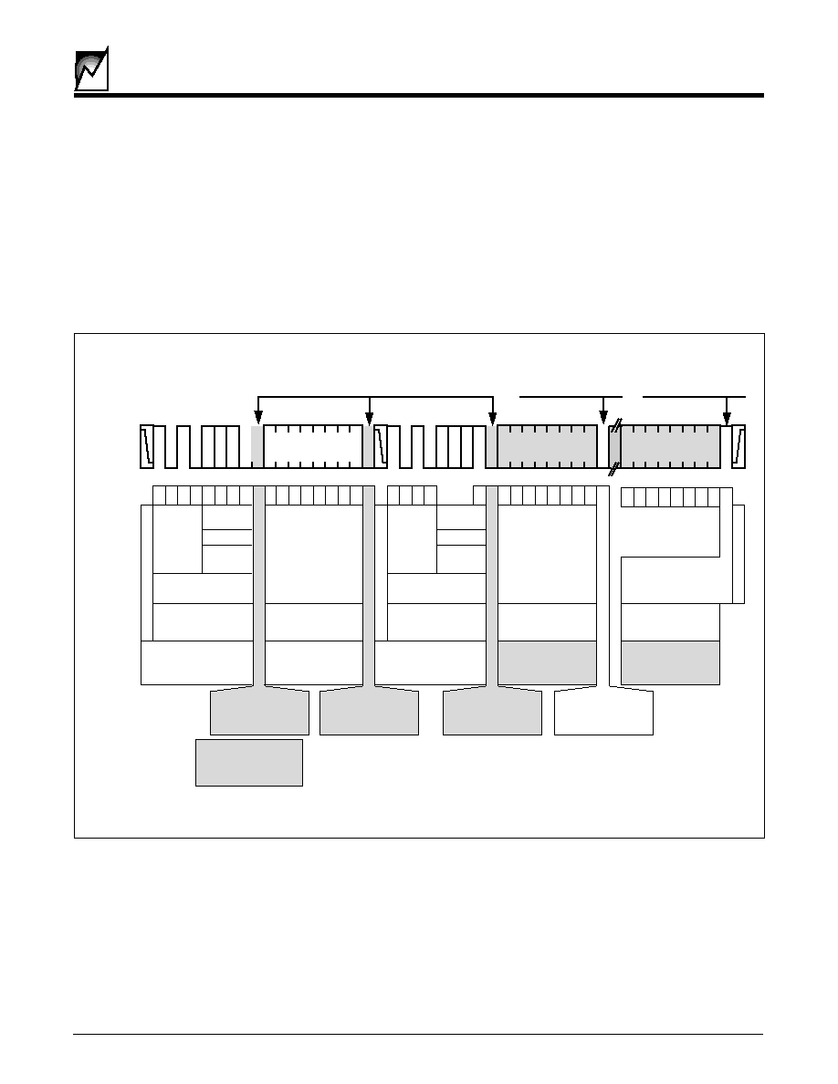
Sequential READ
Sequential READs can be initiated as either a current
address READ or random access READ. The first word is
transmitted as with the other byte read modes (current
address byte READ or random address byte READ);
however, the master now responds with an ACKnowledge,
indicating that it requires additional data from the
SMS29xx. The SMS29xx continues to output data for
each ACKnowledge received. The master terminates the
sequential READ operation by not responding with an
ACKnowledge, and issues a STOP conditions.
During a sequential read operation, the internal address
counter is automatically incremented with each acknowl-
edge signal. For read operations, all address bits are
incremented, allowing the entire array to be read using a
single read command. After a count of the last memory
address, the address counter will `roll-over' and the
memory will continue to output data. See Figure 11 for the
address, acknowledge and data transfer sequence.
FIGURE 11. SEQUENTIAL READ OPERATION (starting with a Random Address READ)
D
7
D
6
D
5
D
4
D
3
D
2
D
1
D
0
D
7
D
6
D
5
D
4
D
3
D
2
D
1
D
0
A
7
A
6
A
5
A
4
A
3
A
2
A
1
A
0
Shading Denotes
SMS29xx
SDA Output Active
S
T
A
R
T
Word Address
S
T
O
P
A
C
K
Acknowledges from SMS29xx
Slave Address
Slave Address
Device
Type
Address
Read/Write
0= Write
Device
Type
Address
SDA Bus
Activity
S
T
A
R
T
Read/Write
1= Read
X
R
W
X
Acknowledge from
Master Receiver
A
C
K
A
C
K
A
C
K
Master sends Read
request to Slave
Master Writes Word
Address to Slave
Master Requests
Data from Slave
Slave sends
Data to Master
Slave Transmitter
to
Master Receiver
Slave Transmitter
to
Master Receiver
Master Transmitter
to
Slave Receiver
1 0 1 0
1 0 1 0
1
0
Slave sends
Data to Master
X
X
R
W
A
10
A
9
A
10
A
9
X
Lack of ACK (low)
determines last
data byte to be read
1
Lack of
Acknowledge from
Master Receiver
Slave Transmitter
to
Master Receiver
Master Transmitter
to
Slave Receiver
Master Transmitter
to
Slave Receiver
Master Transmitter
to
Slave Receiver
Slave Transmitter
to
Master Receiver
Slave Transmitter
to
Master Receiver
Last Data Byte
First Data Byte
2028 ILL13.1
12
SMS2902/SMS2904/SMS2916
2028 5.1 8/2/00
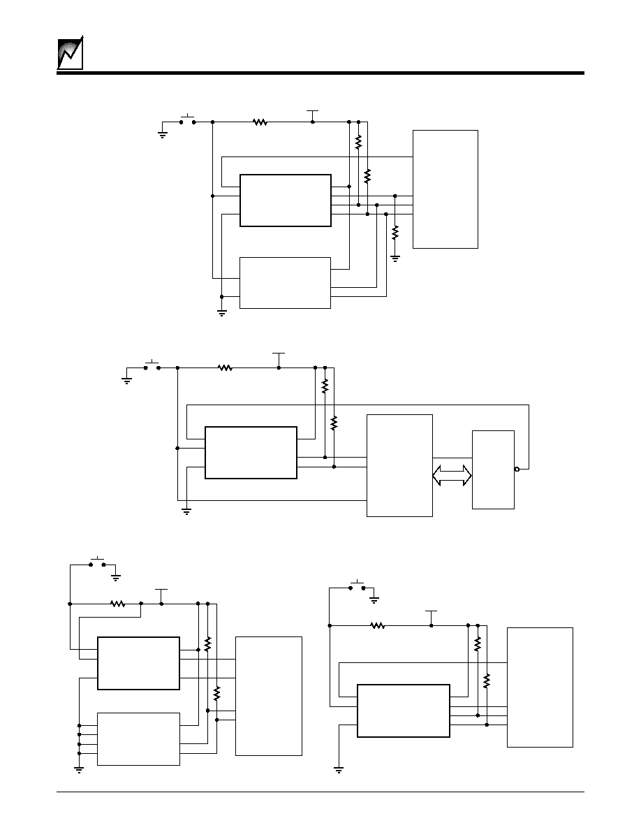
TYPICAL APPLICATION CONFIGURATION USING SYSTEM DECODE LOGIC TO RESET WDI
TYPICAL APPLICATION USING DUAL RESET FUNCTION AND WATCHDOG TIMER
5.0VDC
WDI#
RESET#
NC
GND
VCC
RESET
SCL
SDA
SMS29xx
I/O
I/O
Z80
PB_RST#
2028 T fig13 2.0
RST#
DECODER
2028 T fig14 2.0
VCC
WDI#
RESET#
NC
GND
VCC
RESET
SCL
SDA
SMS29xx
5.0VDC
PBRST#
TOL
GND
VCC
ST#
RST#
RST
SCL
SDA
24C16
I/O
I/O
ALE
8051
Family
Part
ALE
8051
Family
Part
RST
I/O
I/O
1232
GND
RST
VCC = 3.0V or 5.0V
WDI#
RESET#
NC
GND
VCC
RESET
SCL
SDA
SMS29xx
RESET#
SCL
SDA
I
2
C Peripheral
RST
SCL (P0.0)
SDA (P0.1)
ALE
8051 Type
MCU
PB_RST#
2028 T fig12 2.0
From This
To This
SMS2902/SMS2904/SMS2916
13
2028 5.1 8/2/00
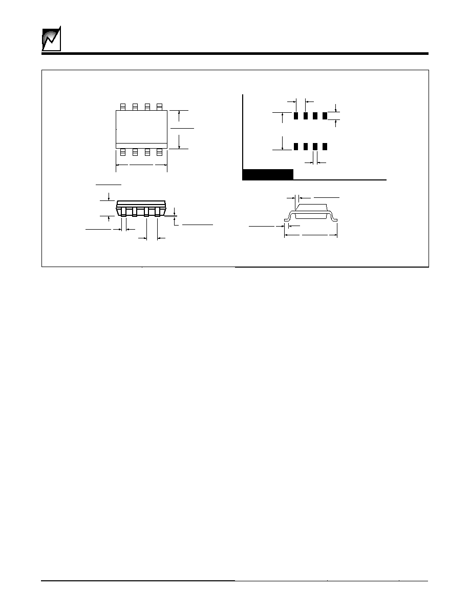
.228 (5.80)
.244 (6.20)
.016 (.40)
.035 (.90)
.020 (.50)
.010 (.25)
x45∞
.0192 (.49)
.0138 (.35)
.061 (1.75)
.053 (1.35)
.0098 (.25)
.004 (.127)
.05 (1.27) TYP.
.275 (6.99) TYP.
.030 (.762) TYP.
8 Places
.050 (1.27) TYP.
.050 (1.270) TYP.
8 Places
.157 (4.00)
.150 (3.80)
.196 (5.00)
1
.189 (4.80)
FOOTPRINT
8pn JEDEC SOIC ILL.2
8 Pin SOIC (Type S) Package JEDEC (150 mil body width)

14
SMS2902/SMS2904/SMS2916
2028 5.1 8/2/00
NOTICE
SUMMIT Microelectronics, Inc. reserves the right to make changes to the products contained in this publication in order
to improve design, performance or reliability. SUMMIT Microelectronics, Inc. assumes no responsibility for the use of
any circuits described herein, conveys no license under any patent or other right, and makes no representation that
the circuits are free of patent infringement. Charts and schedules contained herein reflect representative operating
parameters, and may vary depending upon a user's specific application. While the information in this publication has
been carefully checked, SUMMIT Microelectronics, Inc. shall not be liable for any damages arising as a result of any
error or omission.
SUMMIT Microelectronics, Inc. does not recommend the use of any of its products in life support or aviation applications
where the failure or malfunction of the product can reasonably be expected to cause any failure of either system or to
significantly affect their safety or effectiveness. Products are not authorized for use in such applications unless
SUMMIT Microelectronics, Inc. receives written assurances, to its satisfaction, that: (a) the risk of injury or damage has
been minimized; (b) the user assumes all such risks; and (c) potential liability of SUMMIT Microelectronics, Inc. is
adequately protected under the circumstances.
© Copyright 2000 SUMMIT Microelectronics, Inc.
I
2
C is a trademark of Philips Corporation.
ORDERING INFORMATION
SMS2902 S A
Base Part Number
V
TRIP
Package
S = SOIC
A = 4.5V
B = 4.75V
2.7 = 2.7V
Blank = 4.5V
2028-02 Tree 2.0
SMS2904 S A
Base Part Number
V
TRIP
Package
S = SOIC
A = 4.5V
B = 4.75V
2.7 = 2.7V
Blank = 4.5V
2028-04 Tree 2.0
SMS2916 S A
Base Part Number
V
TRIP
Package
S = SOIC
A = 4.5V
B = 4.75V
2.7 = 2.7V
Blank = 4.5V
2028-16 Tree 2.0