 | –≠–ª–µ–∫—Ç—Ä–æ–Ω–Ω—ã–π –∫–æ–º–ø–æ–Ω–µ–Ω—Ç: SMS44S | –°–∫–∞—á–∞—Ç—å:  PDF PDF  ZIP ZIP |
1
Characteristics subject to change without notice
2047 2.3 10/23/00
EOL 12/16/05
SMS44
SUMMIT
MICROELECTRONICS, Inc.
©SUMMIT MICROELECTRONICS, Inc., 2000 ∑ 300 Orchard City Dr., Suite 131 ∑ Campbell, CA 95008 ∑ Phone 408-378-6461 ∑ FAX 408-378-6586 ∑ www.summitmicro.com
NOTE: THIS PRODUCT HAS REACHED END OF LIFE
!
!
!
!
!
Operational from any of four Voltage Monitoring
Inputs
!
!
!
!
!
Programmability allows monitoring any voltage
between 0.9V and 6.0V with NO external
components
!
!
!
!
!
Programmable Watchdog Timer
!
!
!
!
!
Programmable LongdogTM Timer
!
!
!
!
!
Programmable Reset Pulse Width
!
!
!
!
!
Programmable Power-up sequencing
!
!
!
!
!
Programmable Nonvolatile Combinatorial Logic
for generation of reset and interrupt outputs
!
!
!
!
!
Fault Status Register
Highly Programmble Voltage Supervisory Circuit
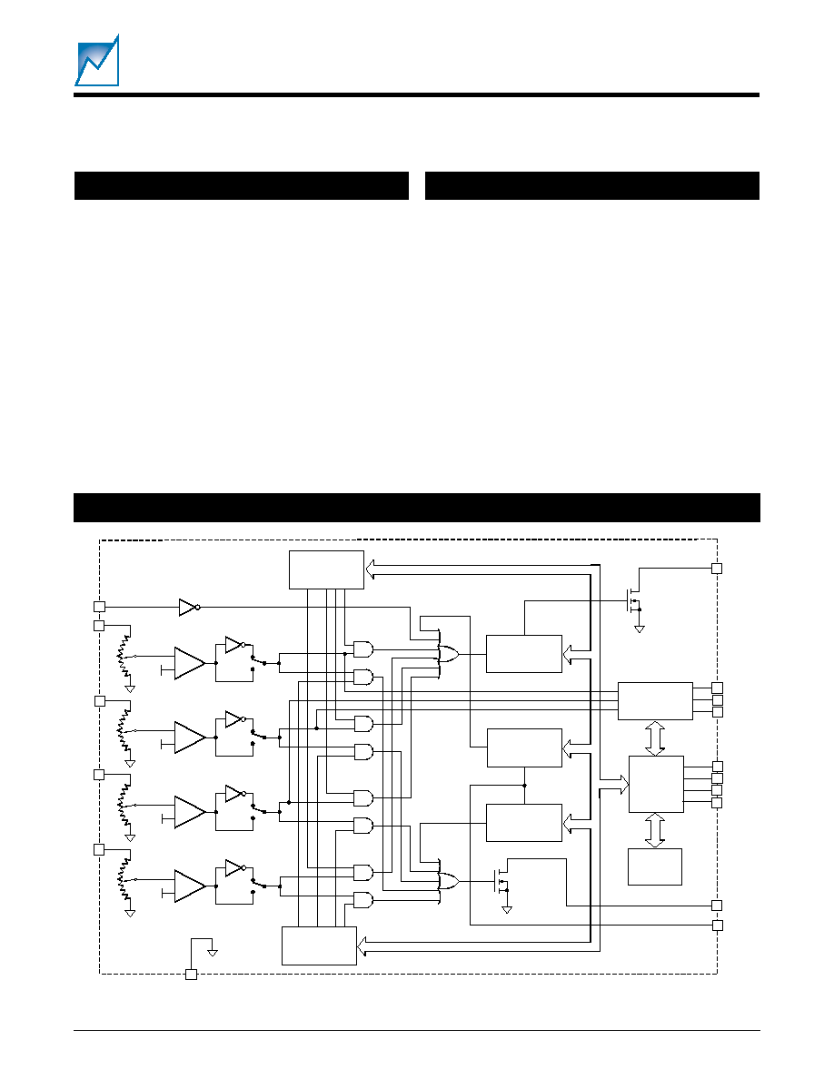
FUNCTIONAL BLOCK DIAGRAM
FEATURES
INTRODUCTION
The SMS44 is a highly programmable voltage supervisory
circuit designed specifically for advanced systems need-
ing to monitor multiple voltages. The SMS44 can monitor
four separate voltages without the need of any external
voltage divider circuitry
The SMS44 watchdog timer has a user programmable
timeout period and it can be placed in an idle mode for
system initialization or system debug. All of the functions
are user accessible through an industry standard 2-wire
serial interface.
2047 BD 1.0
+
≠
REF
NV DAC
+
≠
REF
NV DAC
+
≠
REF
NV DAC
+
≠
REF
NV DAC
RESET
IRQ
RESET
IRQ
RESET
IRQ
V0
16
V1
2
V2
3
V3
14
MR#
1
PROGRAMMABLE
WATCHDOG
TIMER
PROGRAMMABLE
LONGDOG
TIMER
PROGRAMMABLE
RESET PULSE
GENERATOR
SERIAL
BUS
CONTROL
LOGIC
4K-BIT NV
MEMORY
RESET#
PUP#1
11
5
4
SDA
IRQ#
WLDI
9
15
10
PUP#2
PUP#3
13
SCL
A2
7
6
A1
CONFIGURATION
REGISTER
CONFIGURATION
REGISTER
GND
8
RESET
IRQ
12
PROGRAMMABLE
POWER
SEQUENCING
2
SMS44
2047 2.3 10/23/00
SUMMIT MICROELECTRONICS, Inc.
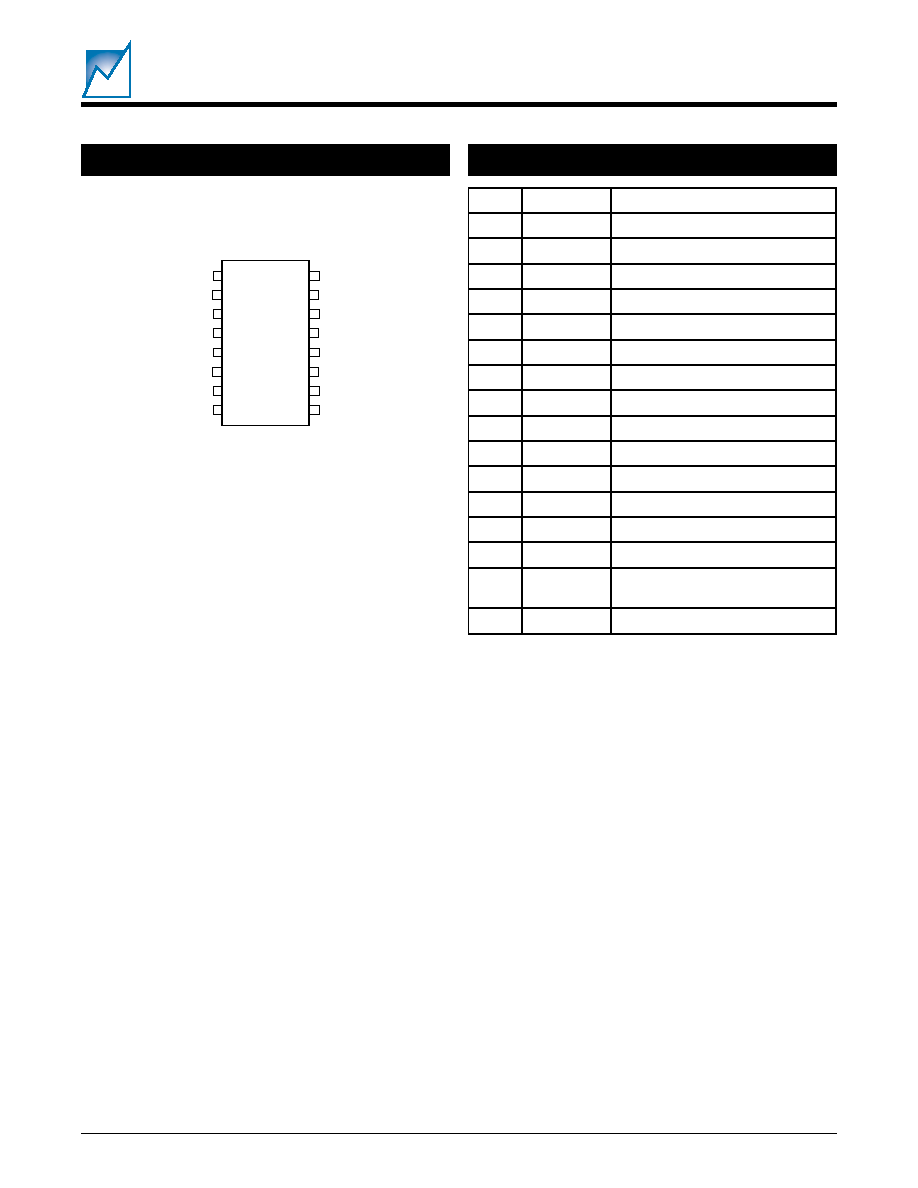
PIN CONFIGURATION
PIN NAMES
MR#
V
1
V
2
PUP#1
PUP#2
A1
A2
GND
V
0
WLDI
V
3
PUP#3
IRQ#
RESET#
SCL
SDA
16-Pin SOIC or
16-Pin SSOP
2047 T PCon 2.0
1
2
3
4
5
6
7
8
16
15
14
13
12
11
10
9
n
i
P
e
m
a
N
n
o
i
t
c
n
u
F
1
#
R
M
t
u
p
n
i
t
e
s
e
r
l
a
u
n
a
M
2
V
1
t
u
p
n
i
r
o
t
i
n
o
m
d
n
a
y
l
p
p
u
s
e
g
a
t
l
o
V
3
V
2
t
u
p
n
i
r
o
t
i
n
o
m
d
n
a
y
l
p
p
u
s
e
g
a
t
l
o
V
4
1
#
P
U
P
t
u
p
t
u
o
d
e
t
t
i
m
r
e
p
p
u
r
e
w
o
P
5
2
#
P
U
P
t
u
p
t
u
o
d
e
t
t
i
m
r
e
p
p
u
r
e
w
o
P
6
1
A
t
u
p
n
i
s
s
e
r
d
d
A
7
2
A
t
u
p
n
i
s
s
e
r
d
d
A
8
D
N
G
n
r
u
t
e
r
y
l
p
p
u
s
r
e
w
o
P
9
A
D
S
O
/
I
a
t
a
d
l
a
i
r
e
S
0
1
L
C
S
k
c
o
l
c
a
t
a
d
l
a
i
r
e
S
1
1
#
T
E
S
E
R
t
u
o
t
e
s
e
R
2
1
#
Q
R
I
t
u
o
t
p
u
r
r
e
t
n
I
3
1
3
#
P
U
P
t
u
p
t
u
o
d
e
t
t
i
m
r
e
p
p
u
r
e
w
o
P
4
1
V
3
t
u
p
n
i
r
o
t
i
n
o
m
d
n
a
y
l
p
p
u
s
e
g
a
t
l
o
V
5
1
I
D
L
W
r
e
m
i
t
g
o
d
g
n
o
l
/
g
o
d
h
c
t
a
W
t
p
u
r
r
e
t
n
i
6
1
V
0
t
u
p
n
i
r
o
t
i
n
o
m
d
n
a
y
l
p
p
u
s
e
g
a
t
l
o
V
2047 Pins Table 2.0
3
2047 2.3 10/23/00
SMS44
SUMMIT MICROELECTRONICS, Inc.
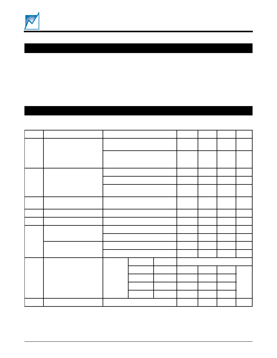
*COMMENT
Stresses beyond the listed Absolute Maximum Ratings may cause
permanent damage to the device. These are stress ratings only, and
functional operation of the device at these or any other conditions
outside those listed in the operational sections of this specification is not
implied. Exposure to any absolute maximum rating for extended
periods may affect device performance and reliability.
Temperature Under Bias ....................... -55∞C to 125∞C
Storage Temperature ............................ -65∞C to 150∞C
Lead Solder Temperature (10 secs) ................... 300 ∞C
Terminal Voltage with Respect to GND:
V
0
, V
1
, V
2
, and V
3
........... -0.3V to 6.0V
All Others ........................ -0.3V to 6.0V
DC OPERATING CHARACTERISTICS
ABSOLUTE MAXIMUM RATINGS*
(
Over Recommended Operating Conditions; Voltages are relative to GND)
2047 Elect TableA 2.1
l
o
b
m
y
S
r
e
t
e
m
a
r
a
P
s
e
t
o
N
.
n
i
M
.
p
y
T
.
x
a
M
t
i
n
U
V
C
C
e
g
a
t
l
o
v
y
l
p
p
u
s
g
n
i
t
a
r
e
p
O
-
t
u
o
t
e
s
e
r
d
il
a
v
a
o
t
s
r
e
f
e
r
.
n
i
m
V
1
d
e
t
a
r
e
n
e
g
g
n
i
e
b
t
u
p
0
.
1
5
.
5
V
t
a
:
s
n
o
i
t
a
r
e
p
o
e
t
i
r
w
/
d
a
e
r
y
r
o
m
e
M
t
a
e
b
t
s
u
m
s
t
u
p
n
i
V
e
h
t
f
o
e
n
o
t
s
a
e
l
V
e
v
o
b
a
r
o
C
C
.
n
i
m
7
.
2
5
.
5
V
I
C
C
t
n
e
r
r
u
c
y
l
p
p
u
S
C
C
V
<
V
6
.
3
V
5
.
5
5
2
0
5
A
µ
V
6
.
3
C
C
V
5
2
0
5
A
µ
y
r
o
m
e
m
r
o
r
e
t
s
i
g
e
r
n
o
i
t
a
r
u
g
i
f
n
o
C
s
s
e
c
c
a
2
A
m
V
H
T
P
e
g
n
a
R
d
l
o
h
s
e
r
h
t
e
l
b
a
m
m
a
r
g
o
r
P
e
g
n
a
r
V
e
g
n
a
r
e
g
a
t
l
o
v
d
l
o
h
s
e
r
h
t
t
e
s
e
R
0
o
t
V
3
)
s
t
n
e
m
e
r
c
n
i
V
m
0
2
(
9
.
0
0
.
6
V
V
H
T
P
d
l
o
h
s
e
r
h
t
e
l
b
a
m
m
a
r
g
o
r
P
0
1
≠
V
H
T
P
0
1
V
m
V
T
S
Y
H
V
T
S
R
s
i
s
e
r
e
t
s
y
h
0
5
V
m
V
L
O
t
u
p
t
u
o
e
g
a
t
l
o
v
w
o
l
#
T
E
S
E
R
I
K
N
I
S
V
,
A
m
2
.
1
=
C
C
V
=
T
S
R
.
n
i
m
3
.
0
V
I
K
N
I
S
V
,
A
m
2
.
1
=
C
C
V
7
.
2
3
.
0
V
t
u
p
t
u
o
e
g
a
t
l
o
v
w
o
l
#
Q
R
I
I
K
N
I
S
V
,
A
m
2
.
1
=
C
C
V
=
T
S
R
.
n
i
m
3
.
0
V
I
K
N
I
S
V
,
A
µ
0
0
2
=
C
C
V
2
.
1
=
3
.
0
V
t
O
T
R
P
e
s
l
u
p
t
e
s
e
r
e
l
b
a
m
m
a
r
g
o
r
P
h
t
d
i
w
1
O
T
R
0
O
T
R
0
0
0
2
5
2
0
3
c
e
s
m
0
1
5
3
0
5
5
6
1
0
5
6
0
0
1
5
3
1
1
1
0
3
1
0
0
2
0
7
2
t
T
S
R
D
y
a
l
e
d
#
T
E
S
E
R
o
t
n
i
V
e
v
i
r
d
r
e
v
o
V
m
0
0
1
0
2
s
µ
4
SMS44
2047 2.3 10/23/00
SUMMIT MICROELECTRONICS, Inc.
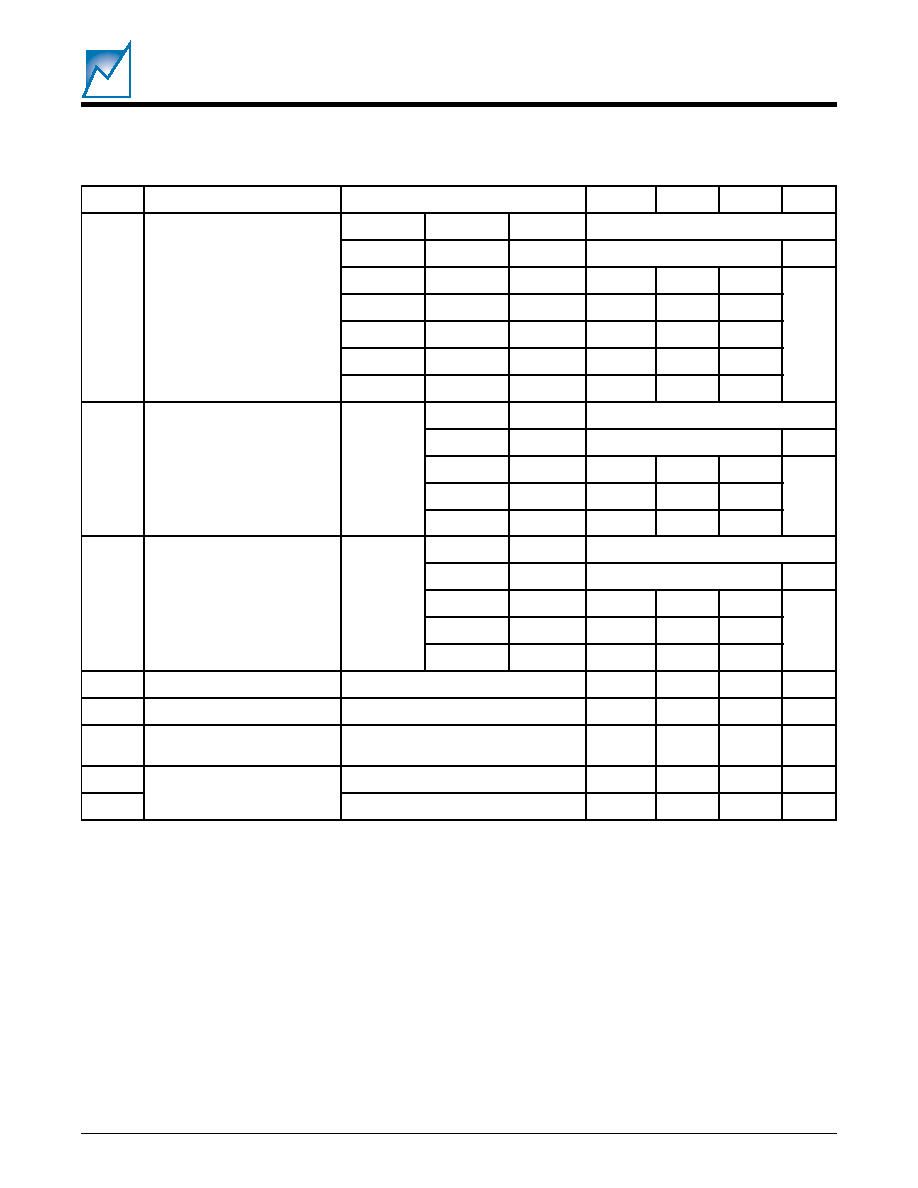
2047 Elect TableB 2.0
l
o
b
m
y
S
r
e
t
e
m
a
r
a
P
s
e
t
o
N
.
n
i
M
.
p
y
T
.
x
a
M
t
i
n
U
t
O
T
D
W
P
g
o
d
h
c
t
a
w
e
l
b
a
m
m
a
r
g
o
r
P
d
o
i
r
e
p
r
e
m
i
t
2
D
W
1
D
W
0
D
W
0
0
0
F
F
O
0
1
1
0
8
2
0
0
4
0
2
5
s
m
1
0
0
0
6
5
0
0
8
0
4
0
1
1
0
1
0
2
1
1
0
0
6
1
0
8
0
2
1
1
0
0
4
2
2
0
0
2
3
0
6
1
4
1
1
1
0
8
4
4
0
0
4
6
0
2
3
8
t
O
T
D
L
P
g
o
d
g
n
o
l
e
l
b
a
m
m
a
r
g
o
r
P
d
o
i
r
e
p
r
e
m
i
t
1
D
L
0
D
L
0
0
F
F
O
0
1
0
2
1
1
0
0
6
1
0
8
0
2
s
m
1
0
0
4
2
2
0
0
2
3
0
6
1
4
1
1
0
8
4
4
0
0
4
6
0
2
3
8
t
Y
L
D
P
X
m
o
r
f
y
a
l
e
d
e
l
b
a
m
m
a
r
g
o
r
P
V
H
T
P
t
u
o
#
P
U
P
o
t
1
-
X
#
P
U
P
0
-
X
#
P
U
P
0
0
F
F
O
0
1
5
2
s
m
1
0
0
5
1
1
0
0
1
I
R
M
t
n
e
r
r
u
c
p
u
ll
u
p
#
R
M
0
0
1
A
µ
T
R
M
h
t
d
i
w
e
s
l
u
p
t
u
p
n
i
#
R
M
0
5
s
n
T
T
S
R
R
M
D
o
t
w
o
l
#
R
M
m
o
r
f
y
a
l
e
D
w
o
l
#
T
E
S
E
R
0
0
1
s
n
V
L
I
d
l
o
h
s
e
r
h
t
t
u
p
n
i
#
R
M
6
.
0
V
V
H
I
7
.
0
◊
V
C
C
V
5
2047 2.3 10/23/00
SMS44
SUMMIT MICROELECTRONICS, Inc.
PIN DESCRIPTIONS
V
0
through V
3
These inputs are used as the voltage monitor inputs and as
the voltage supply for the SMS44. Internally they are diode
ORed and the input with the highest voltage potential will
be the default supply voltage.
The RESET# output will be true if any one of the four inputs
is above 1V. However, for full device operation at least one
of the inputs must be at 2.7V or higher.
The sensing threshold for each input is independently
programmable in 20mV increments from 0.9V to 6.0V.
Also, the occurrence of an under- or over-voltage condi-
tion that is detected as a result of the threshold setting can
be used to generate subsequent action(s), such as RE-
SET# or IRQ#. The programmable nature of the threshold
voltage eliminates the need for external voltage divider
networks.
PUP#1, PUP#2, PUP#3
These are the power-up permitted outputs when the
SMS44 is programmed to provide the sequencing of LDOs
or DC to DC converters. Each delay is independently
enabled and programmable for its duration (
configura-
tion register 7). If all PUP# outputs are enabled the
sequence would be as follows: V
0
above threshold then
delay to PUP#1 turning on; V
1
above threshold then delay
to PUP#2 turning on; V
2
above threshold then delay to
PUP#3 turning on to end the sequence.
MR#
The manual reset input always generates a RESET#
output whenever it is driven low. The duration of the
RESET# output pulse will be initiated when MR# goes low
and it will stay low for the duration of MR# low plus the
programmed reset timeout period (t
PRTO
). If MR# is
brought low during a power-on-sequence of the PUP#s the
sequence will be halted for the reset duration, and will then
resume from the point at which it was interrupted. If MR#
is low the configuration registers can be read or written to
so long as at least one of the V
X
inputs is
2.7V.
RESET#
The reset output is an active low open drain output. It will
be driven low whenever the MR# input is low or whenever
an enabled under-voltage or over-voltage condition exists,
or when a longdog timer expiration exists. The four voltage
monitor inputs are always functioning, but their ability to
generate a reset is programmable (
configuration regis-
ter 4). Refer to figures 1 and 2 for a detailed illustration of
the relationship between MR#, IRQ#, RESET# and the V
IN
levels.
IRQ#
The interrupt output is an active low open-drain output. It
will be driven low whenever the watchdog timer times out
or whenever an enabled under-voltage or over-voltage
condition on a V input exists (
configuration register 6).
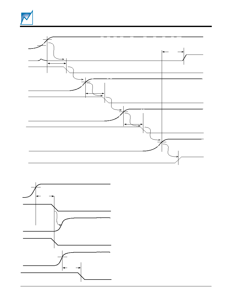
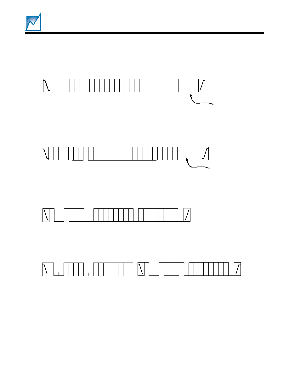
Figure 1. RESET# Timing with MR#
MR#
RESET#
tDMRRST
tPRTO
tPRTO
2047 Fig01 1.0
WLDI
Watchdog and longdog timer interrupt input. A low to high
transition on the WLDI input will clear both the watchdog
and longdog timers, effectively starting a new timeout
period.
If WLDI is stuck low and no low-to-high transition is
received within the programmed t
PWDTO
period (pro-
grammed watch dog timeout) IRQ# will be driven low. If a
transition is still not received within the programmed
t
PLDTO
period (programmed longdog timeout) RESET# will
be driven low. Refer to Figure 3 for a detailed illustration.
Holding WLDI high will block interrupts from occurring but
will not block the longdog from timing out and generating
a reset. Refer to Figure 4 for a detailed illustration of the
relationship between IRQ#, RESET#, and WLDI.
Figure 2. RESET# Timing with IRQ#
IRQ#
RESET#
tPRTO
V
0
-- V
3
VRST
tD
VPTH
2047 Fig02 1.1
6
SMS44
2047 2.3 10/23/00
SUMMIT MICROELECTRONICS, Inc.
A1, A2
A1 and A2 are the address inputs. When addressing the
SMS44 memory or configuration registers the address
inputs distinguish which one of four possible devices
sharing the common bus is being addressed.
SDA
SDA is the serial data input/output pin. It should be tied to
V
CC
through a pull-up resistor.
SCL
SCL is the serial clock input. It should be tied to V
CC
through a pull-up resistor.
Figure 4. Watchdog, Longdog and WLDI Timing
IRQ#
RESET#
WLDI
t0
t0
t0
tPRTO
tPLDTO
2047 Fig04 1.0
Figure 3. Watchdog, Longdog and WLDI Timing
IRQ#
RESET#
tPLDTO
WLDI
t0
t0
t0
t0
t0
tPRTO
tPWDTO
tPLDTO
2047 Fig03 1.0
7
2047 2.3 10/23/00
SMS44
SUMMIT MICROELECTRONICS, Inc.
Table 1. Configuration Register 4
DEVICE OPERATION
2047 Table01 1.0
SUPPLY AND MONITOR FUNCTIONS
The V
0
, V
1
, V
2
and V
3
inputs are internally diode-ORed so
that any one of the four can act as the device supply. The
RESET# output will be guaranteed true so long as one of
the four pins is at or above 1V.
Note: for performing a memory operation (read or
write) and to have the ability to change configura-
tion register contents at least one supply input
must be above 2.7V.
If sequencing is enabled, the designer must insure V
0
is
the primary supply and is the first to become active.
Associated with each input is a comparator with a pro-
grammable threshold for detection of under-voltage con-
ditions on any of the four supply inputs. The threshold can
be programmed in 20mV increments anywhere within the
range of 0.9V to 6.0V. Configuration registers 0, 1, 2, and
3 adjust the thresholds for V
0
, V
1
, V
2
and V
3
respectively.
If the value contained in the register is all zeroes, the
corresponding threshold will be 0.9V. If the contents were
05
HEX
the threshold would then be 1.0V [0.9V + (5
◊
0.02V)]. All four registers are configured as 8-bit registers.
RESET AND IRQ FUNCTIONS
Both the reset and interrupt outputs have four program-
mable sources for activation. Configuration register 4 is
used for selecting the activation source, which can be any
combination of V
0
, V
1
, V
2
and V
3
. A monitor input can only
be programmed to activate on either an under-voltage or
over-voltage condition, but not both conditions.
The RESET# output has two hardwired sources for activa-
tion: the MR# input, and the expiration of the Longdog
timer. RESET# will remain active so long as MR# is low,
and will continue driving the RESET# output for t
PRTO
(programmable reset time out) after MR# returns high.
The MR# input cannot be bypassed or disabled. The
Longdog timer can be bypassed by programming it to the
off or idle mode.
The watchdog is the sole hardwired source for driving the
IRQ# output low. It can effectively be bypassed by
programming it to the off or idle mode. Refer to Figures 1,
2, 3 and 4 for a detailed illustration of the relationships
among the affected signals.
The SMS44 also provides the option of the monitors
triggering on either an under-voltage or over-voltage con-
dition. The low-order four bits of configuration register 5
program these options.
The high order four bits of configuration register 5 are read
only, and their state indicates the sources of interrupts.
Whenever an interrupt is generated the status of the V
inputs will be recorded in the status register. The status
will remain in the register until the device is powered-down
7
B
S
M
6
5
4
3
2
1
0
B
S
L
V
3
V
2
V
1
V
0
V
3
V
2
V
1
V
0
e
c
r
u
o
S
r
e
g
g
i
r
T
T
E
S
E
R
e
c
r
u
o
S
r
e
g
g
i
r
T
Q
R
I
or another interrupt occurs that overwrites the previous
status.
If an interrupt occurs and no bits are set the default
assumption must be the watchdog generated the inter-
rupt.
WATCHDOG AND LONGDOG TIMERS
The SMS44 contains two timers that can be programmed
independently. The Watchdog is intended to be of shorter
duration and will generate an interrupt if it times out. The
3
B
S
M
2
1
0
B
S
L
V
3
V
2
V
1
V
0
s
e
l
b
a
n
e
0
a
g
n
i
t
i
r
W
r
o
f
n
o
i
t
c
e
t
e
d
e
g
a
t
l
o
v
r
e
d
n
u
t
u
p
n
i
V
d
e
t
c
e
l
e
s
e
h
t
0
0
0
0
s
e
l
b
a
n
e
1
a
g
n
i
t
i
r
W
r
o
f
n
o
i
t
c
e
t
e
d
e
g
a
t
l
o
v
r
e
v
o
t
u
p
n
i
V
d
e
t
c
e
l
e
s
e
h
t
1
1
1
1
2047 Table03 1.0
2047 Table02 1.0
Table 2. Configuration Register 5
7
B
S
M
6
5
4
B
S
L
V
3
V
2
V
1
V
0
0
0
0
0
e
h
t
s
e
t
a
c
i
d
n
i
1
a
g
n
i
d
a
e
R
t
p
u
r
r
e
t
n
i
e
h
t
f
o
e
c
r
u
o
s
1
1
1
1
Table 3. Configuration Register 5
8
SMS44
2047 2.3 10/23/00
SUMMIT MICROELECTRONICS, Inc.
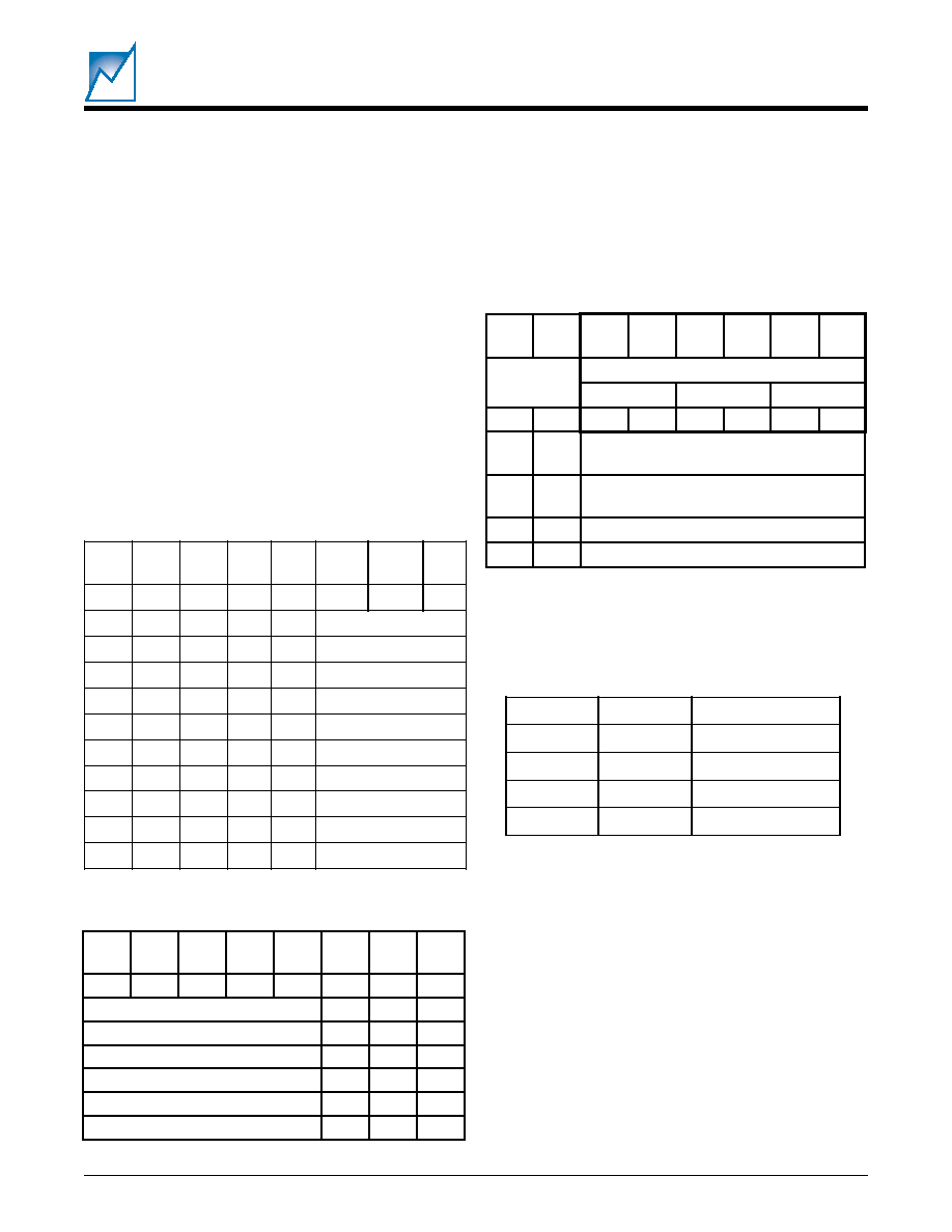
Table 7. PUP Delays
Longdog timer will generally be programmed to be of
longer duration than the watchdog and it will generate a
reset if it times out. Both timers are cleared by a low to high
transition on WLDI and they both start simultaneously.
If the watchdog should timeout the device status will be
recorded in the status register. If the Longdog times out
RESET# will drive low either until a WLDI clear is received
or until t
PRTO
(whichever occurs first), at which time it will
return high. Refer to Figures 3 and 4 illustrating the action
of RESET# and IRQ# with respect to the Watchdog and
Longdog timers and the WLDI input.
If WLDI is held low the timers will free-run generating a
series of interrupts and resets. If WLDI is held high the
interrupt (watchdog) output will be disabled and only the
reset (Longdog) output will be active.
2047 Table04 1.0
7
B
S
M
6
5
4
3
2
1
0
B
S
L
Q
E
S
1
O
T
R
0
O
T
R
1
D
L
0
D
L
2
D
W
1
D
W
0
D
W
x
x
x
0
0
f
f
O
g
o
d
g
n
o
L
x
x
x
0
1
s
m
0
0
6
1
x
x
x
1
0
s
m
0
0
2
3
x
x
x
1
1
s
m
0
0
4
6
x
0
0
x
x
t
O
T
R
P
s
m
5
2
=
x
0
1
x
x
t
O
T
R
P
s
m
0
5
=
x
1
0
x
x
t
O
T
R
P
s
m
0
0
1
=
x
1
1
x
x
t
O
T
R
P
s
m
0
0
2
=
0
x
x
x
x
n
O
e
c
n
e
u
q
e
S
1
x
x
x
x
f
f
O
e
c
n
e
u
q
e
S
Table 4. Configuration Register 6
When the Longdog times out, a reset will be generated.
When reset returns high (after t
PRTO
or after a WLDI
strobe) both timers are reset to time zero. Therefore, if the
Longdog t
PLDTO
is equal to or shorter than the watchdog
t
PWDTO
, the reset will effectively clear the interrupt before
it can drive the output low.
Register 6 is also used to set the programmable reset
timeout period (t
PRTO
) and to select the sequence option.
Sequence Delay Programming
The sequence delays are programmed in register 7. Bit 7
of register 6, must be set to a "0" in order to enable the
sequencing of the PUP# outputs. Sequencing will not
commence until V
0
is above its programmed threshold.
Each PUP# (-3, -2 and -1) is delayed according to the
states of its Bit 1 and Bit 0 as indicated in Table 7.
Refer to Figures 5 and 6 for the detailed timing relationship
of the programmable power-on sequencing.
2047 Table06 1.0
2047 Table07 1.0
7
B
S
M
6
5
4
3
2
1
0
B
S
L
Q
E
S
1
O
T
R
0
O
T
R
1
D
L
0
D
L
2
D
W
1
D
W
0
D
W
F
F
O
0
0
0
s
m
0
0
4
0
1
1
s
m
0
0
8
1
0
0
s
m
0
0
6
1
1
0
1
s
m
0
0
2
3
1
1
0
s
m
0
0
4
6
1
1
1
2047 Table05 1.0
Table 5. Configuration Register 6
Table 6. Configuration Register 7
1
t
i
B
0
t
i
B
t
Y
L
D
P
X
0
0
y
a
l
e
D
)
o
n
(
s
m
0
0
1
y
a
l
e
D
s
m
5
2
1
0
y
a
l
e
D
s
m
0
5
1
1
y
a
l
e
D
s
m
0
0
1
7
B
S
M
6
5
4
3
2
1
0
B
S
L
s
s
e
r
d
d
A
t
c
e
l
e
S
e
t
a
t
S
#
P
U
P
3
#
P
U
P
2
#
P
U
P
1
#
P
U
P
k
c
o
L
0
S
A
1
0
1
0
1
0
x
0
s
d
n
o
p
s
e
r
,
0
1
0
1
s
s
e
r
d
d
a
e
p
y
t
e
c
i
v
e
D
s
n
o
i
t
a
n
i
b
m
o
c
1
A
&
2
A
d
e
s
a
i
b
o
t
y
l
n
o
x
1
s
d
n
o
p
s
e
r
,
1
1
0
1
s
s
e
r
d
d
a
e
p
y
t
e
c
i
v
e
D
s
n
o
i
t
a
n
i
b
m
o
c
1
A
&
2
A
d
e
s
a
i
b
o
t
y
l
n
o
0
x
d
e
l
b
a
n
e
e
t
i
r
w
/
d
a
e
r
n
o
i
t
a
r
u
g
i
f
n
o
C
1
x
t
u
o
d
e
k
c
o
l
e
t
i
r
w
/
d
a
e
r
n
o
i
t
a
r
u
g
i
f
n
o
C
9
2047 2.3 10/23/00
SMS44
SUMMIT MICROELECTRONICS, Inc.
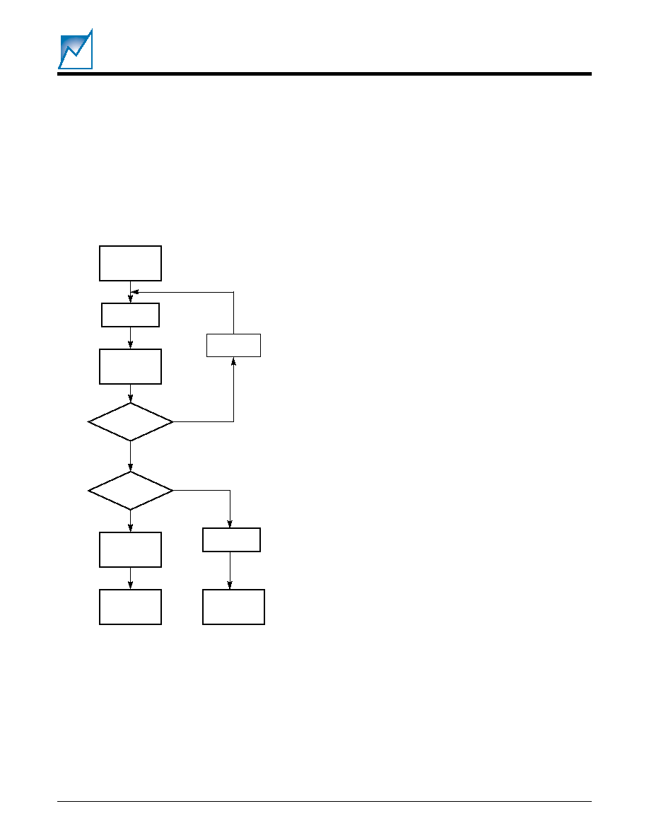
IRQ#
RESET#
V
0
VPTH0
V
1
PUP1#
V
2
PUP2#
V
3
PUP3#
VPTH1
VPTH2
VPTH3
tPRTO
tPDLY1
tPDLY2
tPDLY3
2047 Fig05 1.0
Figure 5. V
X
Input and PUP# Sequence
V0
VPTH0
V1
PUP1#
V2
PUP2#
PUP3#
50ms
50ms
VPTH2
2047 Fig06 1.0
"
"
"
"
"
Figure 6. Timing with Register Contents 22
HEX
10
SMS44
2047 2.3 10/23/00
SUMMIT MICROELECTRONICS, Inc.
The delay from V
PTH0
until PUP#1 low is t
PDLY1
. There is
a similar t
PDLY
X delay for V1 to PUP#2 and V2 to PUP#3.
They are programmed in register 7. See Figure 5.
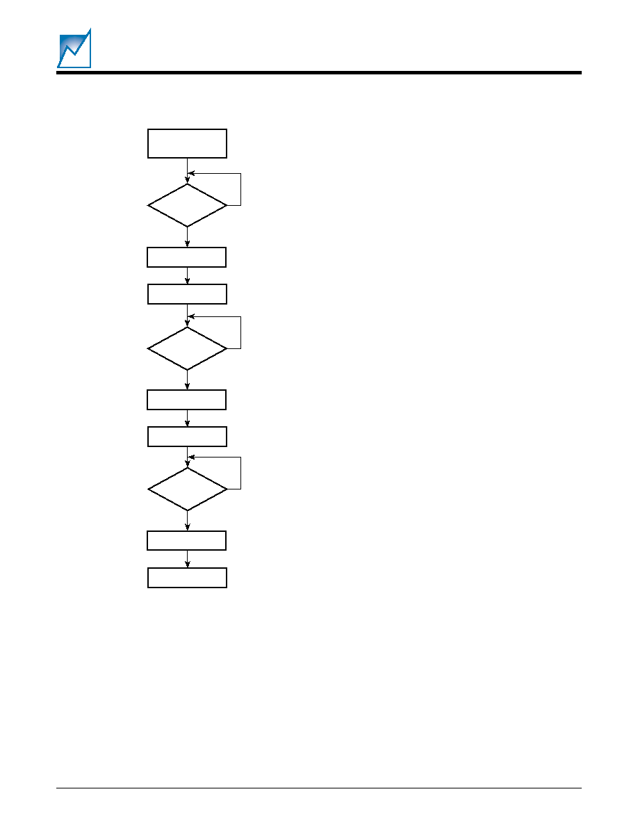
Sequencing will always occur as indicated in the flow
chart.
MEMORY OPERATION
Data for the configuration registers and the memory array
are read and written via an industry standard two-wire
interface. The bus was designed for two-way, two-line
serial communication between different integrated cir-
cuits. The two lines are a serial data line (SDA) and a serial
clock line (SCL). The SDA line must be connected to a
positive supply by a pull-up resistor, located somewhere
on the bus. See Memory Operating Characteristics:
Table 8 and Figure 8.
Figure 7. Sequence Flow Chart
Yes
No
Sequencing
Enabled
V
0
>V
PTH
?
Turn On PUP#1
2047 Fig07 2.1
t
PDLY1
Yes
No
V1
>V
PTH
?
Turn On PUP#2
t
PDLY2
Yes
No
V2
>V
PTH
?
Turn On PUP#3
t
PDLY3
11
2047 2.3 10/23/00
SMS44
SUMMIT MICROELECTRONICS, Inc.
Table 8. Memory Operating Characteristics
Input Data Protocol
The protocol defines any device that sends data onto the
bus as a "transmitter" and any device that receives data as
a "receiver." The device controlling data transmission is
called the "master" and the controlled device is called the
"slave." In all cases the SMS44 will be a "slave" device,
since it never initiates any data transfers.
2047 Table08 2.2
Figure 8. Memory Operating Characteristics
One data bit is transferred during each clock pulse. The
data on the SDA line must remain stable during clock high
time, because changes on the data line while SCL is high
will be interpreted as start or stop condition.
tF
tR
tLOW
tHIGH
tHD:STA
tSU:STA
tBUF
tDH
tHD:DAT
tSU:DAT
tSU:STO
SCL
SDA In
SDA Out
tAA
2047 Fig08 2.1
l
o
b
m
y
S
r
e
t
e
m
a
r
a
P
s
n
o
i
t
i
d
n
o
C
.
n
i
M
.
x
a
M
s
t
i
n
U
f
L
C
S
y
c
n
e
u
q
e
r
f
k
c
o
l
c
L
C
S
0
0
0
1
z
H
k
t
W
O
L
d
o
i
r
e
p
w
o
l
k
c
o
l
C
7
.
4
s
µ
t
H
G
I
H
d
o
i
r
e
p
h
g
i
h
k
c
o
l
C
0
.
4
s
µ
t
F
U
B
e
m
i
t
e
e
r
f
s
u
B
n
o
i
s
s
i
m
s
n
a
r
t
w
e
n
e
r
o
f
e
B
7
.
4
s
µ
t
A
T
S
:
U
S
e
m
i
t
p
u
t
e
s
n
o
i
t
i
d
n
o
c
t
r
a
t
S
7
.
4
s
µ
t
A
T
S
:
D
H
e
m
i
t
d
l
o
h
n
o
i
t
i
d
n
o
c
t
r
a
t
S
0
.
4
s
µ
t
O
T
S
:
U
S
e
m
i
t
p
u
t
e
s
n
o
i
t
i
d
n
o
c
p
o
t
S
7
.
4
s
µ
t
A
A
t
u
p
t
u
o
d
il
a
v
o
t
e
g
d
e
k
c
o
l
C
)
n
e
l
c
y
c
(
A
D
S
d
il
a
v
o
t
w
o
l
L
C
S
3
.
0
5
.
3
s
µ
t
H
D
e
m
i
t
d
l
o
h
t
u
O
a
t
a
D
e
g
n
a
h
c
A
D
S
o
t
)
1
+
n
e
l
c
y
c
(
w
o
l
L
C
S
3
.
0
s
µ
t
R
e
m
i
t
e
s
i
r
A
D
S
d
n
a
L
C
S
0
0
0
1
s
n
t
F
e
m
i
t
ll
a
f
A
D
S
d
n
a
L
C
S
0
0
3
s
n
t
T
A
D
:
U
S
e
m
i
t
p
u
t
e
s
n
I
a
t
a
D
0
5
2
s
n
t
T
A
D
:
D
H
e
m
i
t
d
l
o
h
n
I
a
t
a
D
0
s
n
I
T
A
D
S
d
n
a
L
C
S
r
e
t
li
f
e
s
i
o
N
n
o
i
s
s
e
r
p
p
u
s
e
s
i
o
N
0
0
1
s
n
t
R
W
e
m
i
t
e
l
c
y
c
e
t
i
r
W
5
s
m
12
SMS44
2047 2.3 10/23/00
SUMMIT MICROELECTRONICS, Inc.
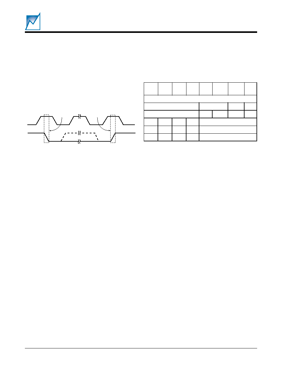
START and STOP Conditions
When both the data and clock lines are HIGH the bus is
said to be not busy. A High-to-Low transition on the data
line, while the clock is HIGH, is defined as the "START"
condition. A Low-to-High transition on the data line, while
the clock is HIGH, is defined as the "STOP" condition. See
Figure 9.
Acknowledge (ACK)
Acknowledge is a software convention used to indicate
successful data transfers. The transmitting device, either
the master or the slave, will release the bus after transmit-
ting eight bits. During the ninth clock cycle the receiver will
pull the SDA line low to ACKnowledge that it received the
eight bits of data.
The SMS44 will respond with an ACKnowledge after
recognition of a START condition and its slave address
byte. If both the device and a write operation are selected
the SMS44 will respond with an ACKnowledge after the
receipt of each subsequent 8-bit word. In the READ mode
the SMS44 transmits eight bits of data, then releases the
SDA line, and monitors the line for an ACKnowledge
signal. If an ACKnowledge is detected and no STOP
condition is generated by the master, the SMS44 will
continue to transmit data. If an ACKnowledge is not
detected the SMS44 will terminate further data transmis-
sions and awaits a STOP condition before returning to the
standby power mode.
Device Addressing
Following a start condition the master must output the
address of the slave it is accessing. The most significant
four bits of the slave address are the device type identifier/
address. For the SMS44 the default is 1010
BIN
. The next
two bits are the Bus Address. The next bit (the 7th) is the
MSB of the memory address.
Figure 9. START and STOP Conditions
Read/Write Bit
The last bit of the data stream defines the operation to be
performed. When set to "1" a read operation is selected;
when set to "0" a write operation is selected.
WRITE OPERATIONS
The SMS44 allows two types of write operations: byte
write and page write. A byte write operation writes a single
byte during the nonvolatile write period (t
WR
). The page
write operation, limited to the memory array, allows up to
16 bytes in the same page to be written during t
WR
.
Byte Write
After the slave address is sent (to identify the slave device
and select either a read or write operation), a second byte
is transmitted which contains the low order 8 bit address
of any one of the 512 words in the array. Upon receipt of
the word address the SMS44 responds with an ACKnowl-
edge. After receiving the next byte of data it again
responds with an ACKnowledge. The master then termi-
nates the transfer by generating a STOP condition, at
which time the SMS44 begins the internal write cycle.
While the internal write cycle is in progress the SMS44
inputs are disabled and the device will not respond to any
requests from the master.
Page Write (memory only)
The SMS44 is capable of a 16-byte page write operation.
It is initiated in the same manner as the byte-write opera-
tion, but instead of terminating the write cycle after the first
data word the master can transmit up to 15 more bytes of
data. After the receipt of each byte the SMS44 will respond
with an ACKnowledge.
The SMS44 automatically increments the address for
subsequent data words. After the receipt of each word, the
low order address bits are internally incremented by one.
7
B
S
M
6
5
4
3
2
1
0
B
S
L
s
t
i
B
s
s
e
r
d
d
A
e
p
y
T
e
c
i
v
e
D
s
u
B
B
S
M
W
/
R
4
4
S
M
S
x
x
x
x
1
0
0
1
r
e
t
s
i
g
e
R
n
o
i
t
a
r
u
g
i
f
n
o
C
1
0
1
0
)
t
l
u
a
f
e
d
(
y
r
o
m
e
M
1
0
1
1
y
r
o
m
e
M
e
t
a
n
r
e
t
l
A
2047 Table09 1.0
Table 9. Slave Addresses
2047 Fig09 1.0
SCL
SDA In
START
Condition
STOP
Condition
13
2047 2.3 10/23/00
SMS44
SUMMIT MICROELECTRONICS, Inc.
The high order bits of the address byte remain constant.
Should the master transmit more than 16 bytes, prior to
generating the STOP condition, the address counter will
"roll over" and the previously written data will be overwrit-
Figure 10. Read and Write Operations
ten. As with the byte-write operation, all inputs are
disabled during the internal write cycle. Refer to Figure 10
for the address, ACKnowledge, and data transfer se-
quence.
Typical Write Operation
(Standard memory device type)
A
C
K
R
/
W
A
C
K
D
7
D
6
D
5
D
4
D
3
D
2
D
1
D
0
A
C
K
S
T
O
P
S
T
A
R
T
Typical Reading Operation
(Alternate memory device type)
Master
SDA
Slave
1
1
0
S
T
A
R
T
A
C
K
B
A
2
B
A
1
A
8
R
/
W
A
C
K
D
7
D
6
D
5
D
4
D
3
D
2
D
1
D
0
A
C
K
S
T
O
P
Master
SDA
Slave
0
1
1 0
A
C
K
R
/
W
A
C
K
D
7
D
6
D
5
D
4
D
3
D
2
D
1
D
0
A
C
K
S
T
O
P
S
T
A
R
T
Writing Configuration Registers
Master
SDA
Slave
0 1
1 0
Master
SDA
Slave
Device Type
Address
Bus
Address
A
7
A
6
A
5
A
4
A
3
A
2
A
1
A
0
A
7
A
6
A
5
A
4
A
3
A
2
A
1
A
0
1
C
7
C
6
C
5
C
4
C
3
C
2
C
1
C
0
A
C
K
R
/
W
A
C
K
S
T
A
R
T
C
7
C
6
C
5
C
4
C
3
C
2
C
1
C
0
Reading the Configuration Register
0 1
1 0
A
C
K
R
/
W
A
C
K
S
T
O
P
S
T
A
R
T
D
7
D
6
D
5
D
4
D
3
D
2
D
1
D
0
0 1
1 0
Up to 15
additional bytes
can be written
before issuing
the stop.
The host may continue
clocking out data so long as
it provides an ACK response
after each byte.
B
A
2
B
A
1
A
8
B
A
2
B
A
1
X
B
A
2
B
A
1
X
B
A
2
B
A
1
X
2047 Fig10 2.1
14
SMS44
2047 2.3 10/23/00
SUMMIT MICROELECTRONICS, Inc.
Acknowledge Polling
When the SMS44 is performing an internal WRITE opera-
tion it will ignore any new START conditions. Since the
device will only return an acknowledge after it accepts the
START the part can be continuously queried until an
acknowledge is issued, indicating that the internal WRITE
cycle is complete. See the flow diagram for the proper
sequence of operations for polling.
READ OPERATIONS
Read operations are initiated with the R/W bit of the
identification field set to "1." T here are two different read
options: 1. Current Address Byte Read, and 2. Random
Address Byte Read
Figure 11. Write Flow Chart
Current Address Read (memory only)
The SMS44 contains an internal address counter which
maintains the address of the last word accessed, incre-
mented by one. If the last address accessed (either a read
or write) was to address location n, the next read operation
would access data from address location n+1 and incre-
ment the current address pointer. When the SMS44
receives the slave address field with the R/W bit set to "1,"
it issues an acknowledge and transmits the 8-bit word
stored at address location n+1. The current address byte
read operation only accesses a single byte of data. The
master does not acknowledge the transfer, but does
generate a stop condition. At this point, the SMS44
discontinues data transmission.
Random Address Read (Register and Memory)
Random address read operations allow the master to
access any memory location in a random fashion. This
operation involves a two-step process. First, the master
issues a write command which includes the start condition
and the slave address field (with the R/W bit set to WRITE),
followed by the address of the word it is to read. This
procedure sets the internal address counter of the SMS44
to the desired address. After the word address acknowl-
edge is received by the master it immediately reissues a
start condition, followed by another slave address field
with the R/W bit set to READ. The SMS44 will respond with
an acknowledge and then transmit the 8 data bits stored
at the addressed location. At this point the master does not
acknowledge the transmission but does generate the stop
condition. The SMS44 discontinues data transmission
and reverts to its standby power mode.
Sequential READ (Memory Only)
Sequential reads can be initiated as either a current
address READ or random access READ. The first word
is transmitted as with the other byte read modes (current
address byte READ or random address byte READ);
however, the master now responds with an ACKnowl-
edge, indicating that it requires additional data from the
SMS44. The SMS44 continues to output data for each
ACKnowledge received. The master terminates the se-
quential READ operation by not responding with an AC-
Knowledge, and issues a stop condition. During a sequen-
tial read operation the internal address counter is auto-
matically incremented with each ACKnowledge signal.
For read operations all address bits are incremented,
allowing the entire array to be read using a single read
command. After a count of the last memory address the
address counter will `roll-over' and the memory will con-
tinue to output data.
Next
Operation
a Write?
ACK
Returned
Issue
Address
Proceed
With
Write
Await
Next
Command
Issue Stop
Issue Slave
Address and
R/W = 0
Issue Stop
Write Cycle
In Progress
Yes
No
Issue Start
2047 Fig11 2.1
Yes
No
15
2047 2.3 10/23/00
SMS44
SUMMIT MICROELECTRONICS, Inc.
0.014 - 0.019
(0.356 - 0.482)
0.004 - 0.012
(0.102 - 0.305)
0.037 - 0.045
(0.940 - 1.143
0.093 - 0.104
(2.362 - 2.642)
0.016 - 0.050
(0.406 - 1.270)
0.050
(1.270)
0.009 - 0.013
(0.229 - 0.330)
0.010 - 0.029
(0.254 - 0.737)
0.291 - 0.299
(7.391 - 7.595)
16 Pin SOIC T
0∫ to 8∫
typ
x45
0.398 - 0.412
(10.109 - 12.465)
0.394 - 0.419
(10.007 - 10.643)
PACKAGES
16 PIN SOIC PACKAGE
ORDERING INFORMATION
SMS44 G
Base Part Number
Package
G = SSOP
S = SOIC
2047 Tree 1.0
16
SMS44
2047 2.3 10/23/00
EOL 12/16/05 SUMMIT MICROELECTRONICS, Inc.
NOTICE
SUMMIT Microelectronics, Inc. reserves the right to make changes to the products contained in this publication in order
to improve design, performance or reliability. SUMMIT Microelectronics, Inc. assumes no responsibility for the use of
any circuits described herein, conveys no license under any patent or other right, and makes no representation that
the circuits are free of patent infringement. Charts and schedules contained herein reflect representative operating
parameters, and may vary depending upon a user's specific application. While the information in this publication has
been carefully checked, SUMMIT Microelectronics, Inc. shall not be liable for any damages arising as a result of any
error or omission.
SUMMIT Microelectronics, Inc. does not recommend the use of any of its products in life support or aviation applications
where the failure or malfunction of the product can reasonably be expected to cause any failure of either system or to
significantly affect their safety or effectiveness. Products are not authorized for use in such applications unless
SUMMIT Microelectronics, Inc. receives written assurances, to its satisfaction, that: (a) the risk of injury or damage has
been minimized; (b) the user assumes all such risks; and (c) potential liability of SUMMIT Microelectronics, Inc. is
adequately protected under the circumstances.
© Copyright 2000 SUMMIT Microelectronics, Inc.
I2C is a trademark of Philips Corporation.
16 PIN SSOP PACKAGE
0 to 8
typ
o
o
11.5∫ to 18.5∫
0.008 - 0.010
(0.19 - 0.25)
0.150 - 0.157
(3.81 - 3.99)
0.25
(0.635)
0.016 - 0.035
(0.41 - 0.89)
0.008 - 0.012
(0.20 - 0.31)
0.055 - 0.061
(1.40 - 1.55)
0.004 - 0.010
(0.12 - 0.25)
0.061 - 0.068
(1.55 - 1.73)
0.002 - 0.007
(0.05 - 0.18)
0.189 - 0.196
(4.80 - 4.98)
0.230 - 0.244
(5.84 - 6.20)
Pin 1