 | –≠–ª–µ–∫—Ç—Ä–æ–Ω–Ω—ã–π –∫–æ–º–ø–æ–Ω–µ–Ω—Ç: SMS46GR04 | –°–∫–∞—á–∞—Ç—å:  PDF PDF  ZIP ZIP |
1
Characteristics subject to change without notice
2083 1.1 06/04/04
SMS46
SUMMIT
MICROELECTRONICS, Inc.
©SUMMIT MICROELECTRONICS, Inc., 2004 ∑ 1717 Fox Dr. ∑ San Jose, CA 95131 ∑ Phone 408-436-9890 ∑ FAX 408-436-9897 ∑
www.summitmicro.com
PRELIMINARY INFORMATION
1
(SEE LAST PAGE)
Operational from any of four Voltage Monitoring
Inputs
Four Independent Programmable Reset Outputs
Programmability allows monitoring any voltage
between 0.6V and 5.6V with no external
components
Programmable 5mV steps in the low range
Programmable Watchdog Timer
Programmable Reset Pulse Width
Fault Status Register
4k-Bit Nonvolatile General Purpose Memory
APPLICATIONS
Desktop/Notebook/Tablet Computers
Multi-voltage Systems
Telecom/Network Servers
Portable Battery-powered Equipment
Set-top Boxes
Data-storage Equipment
Quad Programmable Precision Supervisory Controller With Independent
Resets
and 4k-Bit Nonvolatile Memory
FEATURES
INTRODUCTION
The SMS46 is a highly programmable voltage supply
controller and supervisory circuit designed specifically for
advanced systems that need to monitor multiple voltages.
The SMS46 can monitor four separate voltages without the
need of any external voltage divider circuitry. This allevi-
ates the need for factory-trimmed threshold voltages and
the use of external components to accommodate different
supply voltages and tolerances.
The SMS46 has four programmable independant reset
outputs to control different devices for varying reset condi-
tions such as UV, OV, watchdog and user pushbutton
applications.
The SMS46 watchdog timer has a user programmable
time-out period and it can be placed in an idle mode for
system initialization or system debug. All of the functions
are user accessible through an industry standard I
2
C serial
interface.
Programming of configuration, control and calibration val-
ues by the user is simplified with the SMX3200 interface
adapter and Windows GUI software obtainable from Sum-
mit Microelectronics.
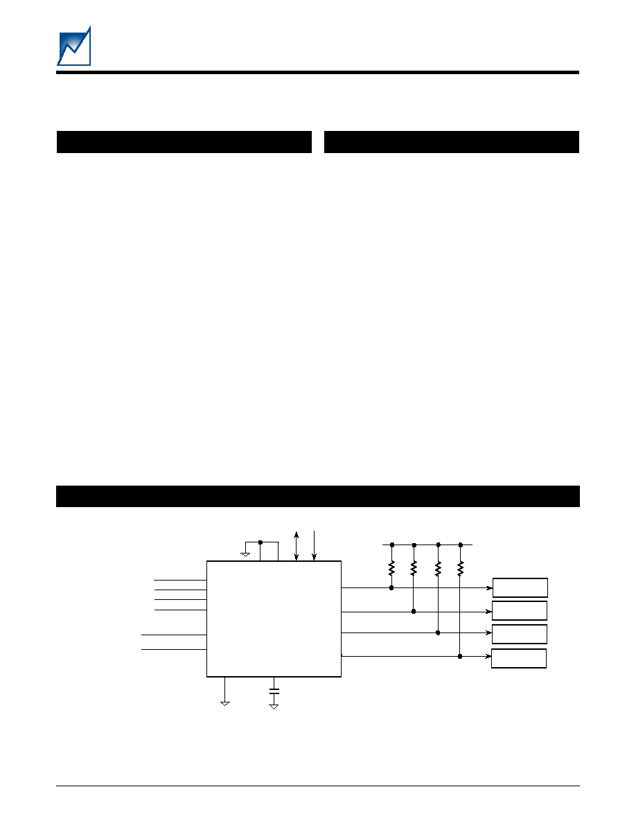
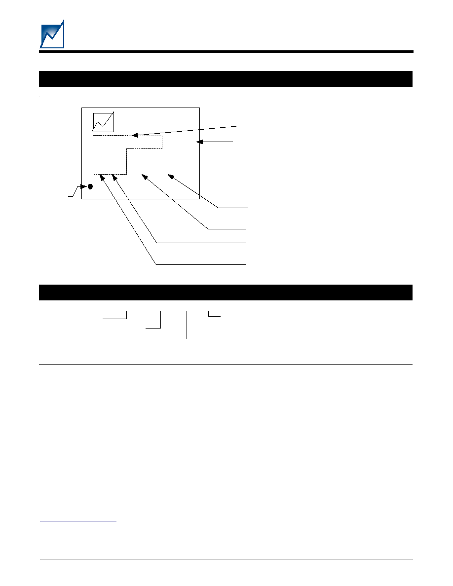
SIMPLIFIED APPLICATION DRAWING
Figure 1 - Precision Quad Power Supply Monitor can monitor any voltage over the range of 0.6V to 5.6V.
One of the four supplies must be above 2.7V to power the SMS46.
V0
V1
V2
V3
RESET#0
RESET#3
VDD_CAP
RESET#1
RESET#2
I
2
C
3.3V
2.5V
1.8V
1.2V
SMS46
A2 A1 SDA SCL
7
6
9
10
1
16
2
3
14
MR#
Monitored
Supplies
15
WLDI
GND
8
13
12
11
5
4
0.1µF
Vpullup (0 to +12V)
uP/DSP
ASIC/FPGA
Logic
LCD
From uP
RESET#
2
SMS46
2083 1.1 06/04/04
SUMMIT MICROELECTRONICS, Inc.
Preliminary Information
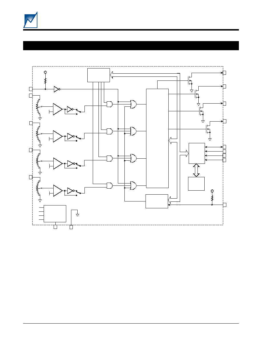
FUNCTIONAL BLOCK DIAGRAM
+
≠
REF
NV DAC
+
≠
REF
NV DAC
+
≠
REF
NV DAC
+
≠
REF
NV DAC
V0
16
V1
2
V2
3
V3
14
MR#
1
PROGRAMMABLE
WATCHDOG
TIMER
SERIAL
BUS
CONTROL
LOGIC
4K-BIT NV
MEMORY
RESET#0
11
SDA
VDD_CAP
WLDI
9
15
10
SCL
A2
7
6
A1
CONFIGURATION
REGISTER
GND
8
VDD_CAP
50k
50k
12
SUPPLY
ARBITRATION
V3
V2
V1
V0
VDD_CAP
RESET#1
4
RESET#2
5
RESET#3
13
PROGRAMMABLE
RESET PULSE
GENERATOR
3
2083 1.1 06/04/04
SMS46
SUMMIT MICROELECTRONICS, Inc.
Preliminary Information
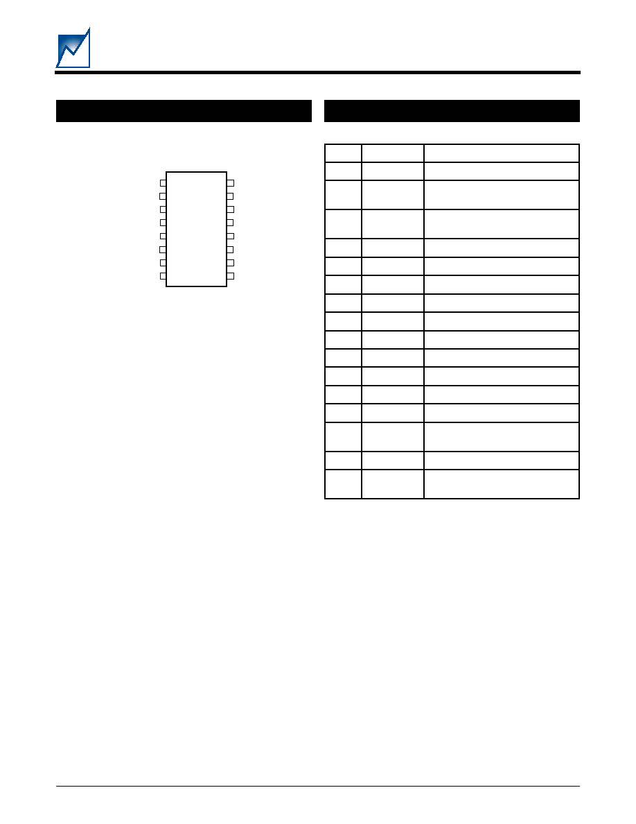
PIN CONFIGURATION
PIN NAMES
MR#
V
1
V
2
RESET#1
RESET#2
A1
A2
GND
V
0
WLDI
V
3
RESET#3
VDD_CAP
RESET#0
SCL
SDA
1
2
3
4
5
6
7
8
16
15
14
13
12
11
10
9
n
i
P
e
m
a
N
n
o
i
t
c
n
u
F
1
#
R
M
t
u
p
n
i
t
e
s
e
r
l
a
u
n
a
M
2
V
1
r
o
ti
n
o
m
d
n
a
y
l
p
p
u
s
e
g
a
tl
o
V
t
u
p
n
i
3
V
2
r
o
ti
n
o
m
d
n
a
y
l
p
p
u
s
e
g
a
tl
o
V
t
u
p
n
i
4
1
#
T
E
S
E
R
t
u
p
t
u
o
1
#
t
e
s
e
R
5
2
#
T
E
S
E
R
t
u
p
t
u
o
2
#
t
e
s
e
R
6
1
A
t
u
p
n
i
s
s
e
r
d
d
A
7
2
A
t
u
p
n
i
s
s
e
r
d
d
A
8
D
N
G
n
r
u
t
e
r
y
l
p
p
u
s
r
e
w
o
P
9
A
D
S
O
/I
a
t
a
d
l
a
ir
e
S
0
1
L
C
S
k
c
o
l
c
a
t
a
d
l
a
ir
e
S
1
1
0
#
T
E
S
E
R
t
u
p
t
u
o
0
#
t
e
s
e
R
2
1
P
A
C
_
D
D
V
t
u
p
t
u
o
y
l
p
p
u
s
r
e
w
o
P
3
1
3
#
T
E
S
E
R
t
u
p
t
u
o
3
#
t
e
s
e
R
4
1
V
3
r
o
ti
n
o
m
d
n
a
y
l
p
p
u
s
e
g
a
tl
o
V
t
u
p
n
i
5
1
I
D
L
W
t
p
u
r
r
e
t
n
i
r
e
m
it
g
o
d
h
c
t
a
W
6
1
V
0
r
o
ti
n
o
m
d
n
a
y
l
p
p
u
s
e
g
a
tl
o
V
t
u
p
n
i
4
SMS46
2083 1.1 06/04/04
SUMMIT MICROELECTRONICS, Inc.
Preliminary Information
DC OPERATING CHARACTERISTICS
(Over Recommended Operating Conditions; Voltages are relative to GND)
l
o
b
m
y
S
r
e
t
e
m
a
r
a
P
s
e
t
o
N
.
n
i
M
.
p
y
T
.
x
a
M
t
i
n
U
D
D
V
e
g
a
t
l
o
v
y
l
p
p
u
s
g
n
i
t
a
r
e
p
O
-
t
u
o
t
e
s
e
r
d
il
a
v
a
o
t
s
r
e
f
e
r
.
n
i
m
V
1
d
e
t
a
r
e
n
e
g
g
n
i
e
b
t
u
p
0
.
1
5
.
5
V
t
a
:
s
n
o
i
t
a
r
e
p
o
e
t
i
r
w
/
d
a
e
r
y
r
o
m
e
M
t
a
e
b
t
s
u
m
s
t
u
p
n
i
V
e
h
t
f
o
e
n
o
t
s
a
e
l
.
n
i
m
D
D
V
e
v
o
b
a
r
o
7
.
2
5
.
5
V
D
D
I
t
n
e
r
r
u
c
y
l
p
p
u
S
D
D
V
V
;
V
5
.
5
0
V
;
V
7
.
4
t
n
i
o
p
p
i
r
t
1
V
,
2
,
V
3
s
t
u
p
t
u
o
ll
a
;
D
D
V
=
#
R
M
;
D
N
G
=
g
n
i
t
a
o
l
f
0
0
2
0
0
4
A
µ
y
r
o
m
e
m
r
o
r
e
t
s
i
g
e
r
n
o
i
t
a
r
u
g
i
f
n
o
C
s
s
e
c
c
a
3
A
m
V
H
T
P
e
g
n
a
R
d
l
o
h
s
e
r
h
t
e
l
b
a
m
m
a
r
g
o
r
P
)
e
g
n
a
r
w
o
l
(
V
e
g
n
a
r
e
g
a
t
l
o
v
d
l
o
h
s
e
r
h
t
t
e
s
e
R
0
o
t
V
3
)
s
t
n
e
m
e
r
c
n
i
V
m
5
(
6
.
0
5
7
8
.
1
V
V
H
T
P
e
g
n
a
R
d
l
o
h
s
e
r
h
t
e
l
b
a
m
m
a
r
g
o
r
P
)
e
g
n
a
r
h
g
i
h
(
V
e
g
n
a
r
e
g
a
t
l
o
v
d
l
o
h
s
e
r
h
t
t
e
s
e
R
0
o
t
V
3
)
s
t
n
e
m
e
r
c
n
i
V
m
5
1
(
8
.
1
5
2
6
.
5
V
V
C
C
A
H
T
P
d
l
o
h
s
e
r
h
t
e
l
b
a
m
m
a
r
g
o
r
P
y
c
a
r
u
c
c
A
V
H
T
P
d
l
o
h
s
e
r
h
t
d
e
m
m
a
r
g
o
r
p
e
h
t
s
i
V
e
h
t
n
i
h
t
i
w
t
n
i
o
p
t
e
s
H
T
P
e
g
n
a
R
0
.
1
≠
V
H
T
P
0
.
1
%
V
T
S
Y
H
V
T
S
R
s
i
s
e
r
e
t
s
y
h
w
o
l
e
b
1
e
t
o
N
e
e
S
D
B
T
V
m
R
U
P
e
c
n
a
t
s
i
s
e
r
p
u
-
ll
u
P
s
n
i
p
I
D
L
W
d
n
a
#
R
M
0
5
k
V
L
O
t
u
p
t
u
o
e
g
a
t
l
o
v
w
o
L
I
K
N
I
S
V
,
A
m
1
=
P
A
C
_
D
D
V
V
7
.
2
3
.
0
V
I
K
N
I
S
V
,
A
µ
0
0
2
=
P
A
C
_
D
D
V
V
0
.
1
=
3
.
0
V
V
L
I
d
l
o
h
s
e
r
h
t
t
u
p
n
I
6
.
0
V
V
H
I
7
.
0
◊
V
D
D
V
*Note -
Stresses beyond the listed Absolute Maximum Ratings may
cause permanent damage to the device. These are stress ratings only,
and functional operation of the device at these or any other conditions
outside those listed in the operational sections of this specification is not
implied. Exposure to any absolute maximum rating for extended
periods may affect device performance and reliability.
Temperature Under Bias ........................ ≠55∞C to 125∞C
Storage Temperature ............................. ≠65∞C to 150∞C
Lead Solder Temperature (10s) ........................... 300 ∞C
Terminal Voltage with Respect to GND:
V
0
, V
1
, V
2
, and V
3
......... ≠0.3V to 6.0V
RESET#0-3 ..................... ≠0.3V to 15V
All Others ....................... ≠0.3V to 6.0V
Junction Temperature........................................150∞C
ESD Rating per JEDEC...................................2000V
Latch-Up testing per JEDEC...........................±100mA
ABSOLUTE MAXIMUM RATINGS*
RECOMMENDED OPERATING CONDITIONS
Industrial Temperature Range............... ≠40
∫
C to +85
∫
C.
Commercial Temperature Range..............≠5
∫
C to +70
∫
C.
V
SUPPLY
Supply Voltage............................2.7V to 5.5V
V
SUPPLY
= Device supply voltage provided by the
highest V
X
input.
Package Thermal Resistance (
JA)
16 Lead SSOP.........................................23
o
C/W
Moisture Classification Level 1 (MSL 1) per J-STD- 020
RELIABILITY CHARACTERISTICS
Data Retention.........................................100 Years
Endurance........................................100,000 Cycles
Note 1: Low Range Hysteresis = 4.2 X (Vtrip - 0.5 volts) mV. For Vtrip = 1.0 volts, Hysteresis = 2.1 mV (0.21 %),
High Range Hysteresis = 12.6 X (Vtrip -0.5 volts) mV. For Vtrip = 5.0 volts, Hysteresis = 56.7 mV (1.13%).
5
2083 1.1 06/04/04
SMS46
SUMMIT MICROELECTRONICS, Inc.
Preliminary Information
l
o
b
m
y
S
r
e
t
e
m
a
r
a
P
s
e
t
o
N
.
n
i
M
.
p
y
T
.
x
a
M
t
i
n
U
t
O
T
R
P
e
s
l
u
p
t
e
s
e
r
e
l
b
a
m
m
a
r
g
o
r
P
h
t
d
i
w
9
1
5
2
1
3
s
m
8
3
0
5
3
6
s
m
5
7
0
0
1
5
2
1
s
m
0
5
1
0
0
2
0
5
2
s
m
t
T
S
R
D
y
a
l
e
d
#
T
E
S
E
R
o
t
n
i
V
e
v
i
r
d
r
e
v
o
V
m
0
0
1
0
2
s
µ
t
O
T
D
W
P
g
o
d
h
c
t
a
W
e
l
b
a
m
m
a
r
g
o
r
P
d
o
i
r
e
p
r
e
m
i
t
F
F
O
--
0
0
3
0
0
4
0
0
5
s
m
0
0
6
0
0
8
0
0
0
1
s
m
0
0
2
1
0
0
6
1
0
0
0
2
s
m
0
0
4
2
0
0
2
3
0
0
0
4
0
0
8
4
0
0
4
6
0
0
0
8
s
m
T
R
M
h
t
d
i
w
e
s
l
u
p
t
u
p
n
i
#
R
M
g
n
i
r
b
o
t
d
e
r
i
u
q
e
r
e
s
l
u
p
m
u
m
i
n
i
M
e
v
i
t
c
a
t
e
s
e
R
0
0
3
s
n
T
T
S
R
R
M
D
o
t
w
o
l
#
R
M
m
o
r
f
y
a
l
e
D
w
o
l
#
T
E
S
E
R
0
0
2
s
n
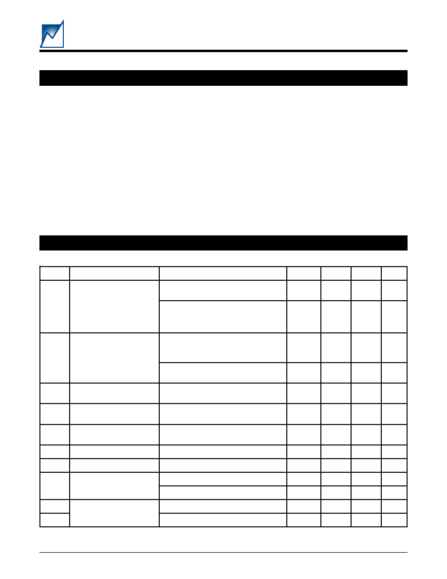
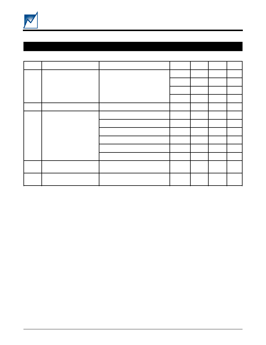
AC OPERATING CHARACTERISTICS
(Over Recommended Operating Conditions; Voltages are relative to GND)
6
SMS46
2083 1.1 06/04/04
SUMMIT MICROELECTRONICS, Inc.
Preliminary Information
PIN DESCRIPTIONS
V
0
, V
1
, V
2
, V
3
(16, 2, 3, 14)
These inputs are used as the voltage monitor inputs and
as the voltage supply for the SMS46. Internally they are
actively diode ORed and the input with the highest voltage
potential will be the default supply voltage (VDD_CAP).
The RESET# outputs will be valid if any one of the four
inputs is above 1V. However, for full device operation at
least one of the inputs must be at 2.7V or higher.
The sensing threshold for each input is independently
programmable in 5mV increments from 0.6V to 1.875V or
15mV increments from 1.8V to 5.625V. Also, the occur-
rence of an under- or over-voltage condition that is detected
as a result of the threshold setting can be used to generate
a RESET#0-3. The programmable nature of the threshold
voltage eliminates the need for external voltage divider
networks.
GND
Power supply return.
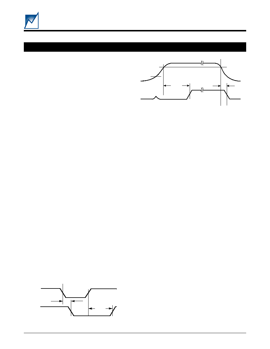
MR# (1)
The manual reset input always generates a RESET#0-3
output whenever it is driven low. The duration of the
RESET# output pulse will be initiated when MR# goes low
and it will stay low for the duration of MR# low pulse plus
the programmed reset time-out period (t
PRTO
). MR# must
be held low during a configuration register write or read.
This signal is pulled up internally through a 50k
resistor.
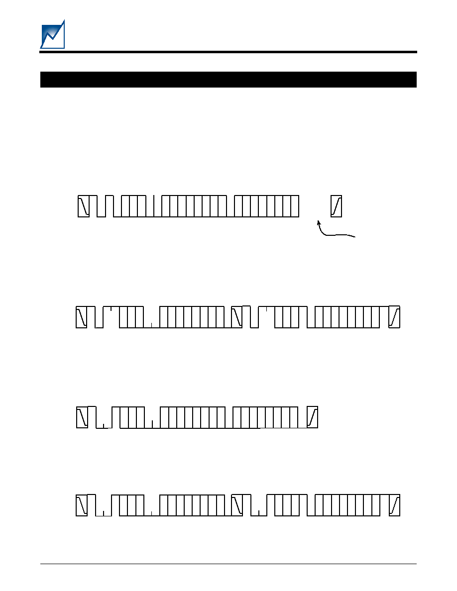
RESET#0-3 (11, 4, 5, 13)
The reset outputs are active low open drain outputs. They
are driven low whenever the MR# input is low or whenever
a triggering under-voltage or over-voltage condition exists
on the corresponding input channel or when the Watchdog
timer expires. The four voltage monitor inputs are always
functioning, but their ability to generate a reset is program-
mable (configuration register 4). Refer to Figures 2, 3 and
5 for a detailed illustration of the relationship between MR#,
RESET#0-3 and the V
IN
levels.
Figure 2 - RESET# Timing with MR#
VDD_CAP (12)
The VDD_CAP pin connects to the internal supply voltage
for the SMS46. A capacitor is placed on this pin to filter
supply noise as well as hold up the device in the event of
power failure. The voltage on this node is determined by the
highest input voltage. Loading of this pin should be
minimized to prevent excessive power dissipation in the
part.
WLDI (15)
Watchdog input. A low to high transition on the WLDI input
will clear the watchdog timer, effectively starting a new
time-out period. This signal is pulled up internally through
a 50k
resistor.
If WLDI is stuck low and no low-to-high transition is received
within the programmed t
PWDTO
period (programmed watch
dog time-out) the RESET#0-3 outputs will be driven low.
Holding WLDI high will not block the Watchdog from timing
out and generating a reset. Refer to Figure 4 for a detailed
illustration of the relationship between RESET#0-3 and
WLDI.
A1, A2 (6, 7)
A1 and A2 are the address inputs. When addressing the
SMS46 memory or configuration registers the address
inputs distinguish which one of four possible devices
sharing the common bus is being addressed.
SDA (9)
SDA is the serial data input/output pin. It should be tied to
V
DD_CAP
through a pull-up resistor.
Figure 3 - RESET# Timing
MR#
RESET#
tDMRRST
tPRTO
RESET#
tPRTO
V
0
-- V
3
tDRST
VPTH-UV
7
2083 1.1 06/04/04
SMS46
SUMMIT MICROELECTRONICS, Inc.
Preliminary Information
SCL (10)
SCL is the serial clock input. It should be tied to V
DD_CAP
through a pull-up resistor.
Figure 4 - Watchdog and WLDI Timing
tPRTO
2047 Fig04 3.0
RESET#
WLDI
t0
t0
t0
t0
t0
tPRTO
tPWDTO
tPWDTO
Figure 5 - V
0-1
Inputs and Resulting RESET# Behavior with V
0
set to UV and V
1
set to OV sensing.
V
0
V
P T H - U V
R E S E T # 0
t
D R S T
V
1
V
P T H - O V
R E S E T # 1
t
P R T O
t
D R S T
t
P R T O
PIN DESCRIPTIONS (CONTINUED)
8
SMS46
2083 1.1 06/04/04
SUMMIT MICROELECTRONICS, Inc.
Preliminary Information
Table 2. Configuration Register 4
DEVICE OPERATION AND CONFIGURATION REGISTERS
SUPPLY AND MONITOR FUNCTIONS
The V
0
, V
1
, V
2,
and V
3
inputs are internally ORed so that
any one of the four can act as the device supply. The
RESET# outputs will be guaranteed true so long as one of
the four pins is at or above 1V.
Note: for performing a memory operation (Read
or Write) and to have the ability to change
configuration register contents at least one sup-
ply input must be above 2.7V.
Read/Write operations require a 0.1µF capacitor from the
VDD_CAP node to GND. For optimum performance
connect capacitors from each of the Vx inputs to GND.
Locate the capacitors as physically close to the SMS46 as
possible.
Associated with each input is a comparator with a program-
mable threshold for detection of under-voltage or over-
voltage conditions on any of the four supply inputs. The
threshold can be programmed in 5mV increments any-
where within the range of 0.6V to 1.875V or 15mV incre-
ments within the range of 1.8V to 5.625V. Configuration
registers 0, 1, 2, and 3 adjust the thresholds for V
0
, V
1
, V
2,
and V
3
respectively.
If the value contained in any register is all zeroes, the
corresponding threshold will be 0.6V. If the contents were
low range 05
HEX
the threshold would then be 0.625V [0.6V
+ (5
◊
0.005V)]. All four registers are configured as 8-Bit
registers.
Table 1. Configuration Registers 0, 1, 2, and 3
RESET# FUNCTION
Each RESET# output has a programmable source for
activation. Configuration register 4 is used for enabling the
activation source. A monitor input can be programmed to
activate on either an under-voltage or over-voltage condi-
tion, but not both conditions. When this condition ceases,
each individual RESET# output will remain active for t
PRTO
(programmable reset time-out). The reset threshold voltage
range for V0 to V3 can be set for 5mV increments below
1.875V (low Range = "0") or for 15mV increments above
1.8V (high range = "1") using Bits D3:0.
The RESET#0-3 outputs have two hardwired sources for
activation: the MR# input and Watchdog timer. All
RESET# outputs will remain active so long as MR# is low,
and will continue driving the RESET# outputs for t
PRTO
(programmable reset time out) after MR# returns high. The
MR# input cannot be bypassed or disabled.
Refer to Figures 1, 2 and 3 for a detailed illustration of the
relationships among the affected signals.
The SMS46 provides the option of the monitors triggering
on either an under-voltage or over-voltage condition. The
low-order four bits of configuration register 5 program these
options.
WATCHDOG TIMER
The SMS46 contains an independent timer that can be
programmed. The Watchdog generates all RESET#s if it
times out. The timer is cleared by a low to high transition
on WLDI and will reset all four RESET#.
If the watchdog should time-out the device status can be
monitored in the status register (Table 4). Refer to Figure
3 which illustrates the action of RESET#0-3 with respect to
the Watchdog timer and the WLDI input.
7
D
B
S
M
6
D
5
D
4
D
3
D
2
D
1
D
0
D
B
S
L
n
o
i
t
c
A
V
3
V
2
V
1
V
0
V
3
V
2
V
1
V
0
e
l
b
a
n
E
r
e
g
g
i
r
T
T
E
S
E
R
e
g
n
a
R
d
l
o
h
s
e
r
h
T
e
g
a
t
l
o
V
t
c
e
l
e
S
0
0
0
0
w
o
L
e
g
n
a
R
1
1
1
1
h
g
i
H
e
g
n
a
R
7
D
B
S
M
6
D
5
D
4
D
3
D
2
D
1
D
0
D
B
S
L
n
o
i
t
c
A
1
1
1
1
1
1
1
1
V
5
2
6
.
5
=
t
n
e
m
t
s
u
j
d
a
d
l
o
h
s
e
r
h
t
t
s
e
h
g
i
H
)
e
g
n
a
R
h
g
i
H
(
0
0
0
0
0
0
0
0
V
6
.
0
=
t
n
e
m
t
s
u
j
d
a
d
l
o
h
s
e
r
h
t
t
s
e
w
o
L
)
e
g
n
a
R
w
o
L
(
0
0
0
0
0
1
1
0
6
(
+
V
6
.
0
=
d
l
o
h
s
e
r
h
T
◊
V
5
2
6
.
0
=
)
V
5
0
0
.
0
)
.
g
.
e
(
9
2083 1.1 06/04/04
SMS46
SUMMIT MICROELECTRONICS, Inc.
Preliminary Information
Table 5. Configuration Register 6 (D3 through D7)
Note 1 - Read Only bit D7 is set to a 1. Read only bits
D4 and D3 are revision control and the value indi-
cates the status code of the device (ie. 01 is status
code 1).
Table 4. Status Register 5 (D4 through D7)
Table 3. Configuration Register 5 (D0 through D3)
If WLDI is held low the timer will free-run generating a series
of resets. When RESET# returns high (after t
PRTO
) the
timer is reset to time zero. Register 6 is also used to set
the programmable reset time-out period (t
PRTO
).
Table 6. Configuration Register 6 (D0, D1, D2)
n
o
i
t
c
A
3
D
B
S
M
2
D
1
D
0
D
B
S
L
V
3
V
2
V
1
V
0
s
e
l
b
a
n
e
0
a
g
n
i
t
i
r
W
r
o
f
n
o
i
t
c
e
t
e
d
e
g
a
t
l
o
v
r
e
d
n
u
t
u
p
n
i
V
d
e
t
c
e
l
e
s
e
h
t
0
0
0
0
s
e
l
b
a
n
e
1
a
g
n
i
t
i
r
W
r
o
f
n
o
i
t
c
e
t
e
d
e
g
a
t
l
o
v
r
e
v
o
t
u
p
n
i
V
d
e
t
c
e
l
e
s
e
h
t
1
1
1
1
2
D
1
D
0
D
B
S
L
n
o
i
t
c
A
2
D
W
1
D
W
0
D
W
F
F
O
0
0
0
s
m
0
0
4
0
1
1
s
m
0
0
8
1
0
0
s
m
0
0
6
1
1
0
1
s
m
0
0
2
3
1
1
0
s
m
0
0
4
6
1
1
1
7
D
B
S
M
6
D
5
D
4
D
3
D
d
a
e
R
1
y
l
n
O
1
O
T
R
0
O
T
R
d
a
e
R
y
l
n
O
d
a
e
R
y
l
n
O
n
o
i
t
c
A
1
0
0
x
x
t
O
T
R
P
s
m
5
2
=
1
0
1
x
x
t
O
T
R
P
s
m
0
5
=
1
1
0
x
x
t
O
T
R
P
s
m
0
0
1
=
1
1
1
x
x
t
O
T
R
P
s
m
0
0
2
=
Table 7. Configuration Register 7 (D7, D6) Bits D5
through D0 are not used.
7
D
B
S
M
6
D
n
o
i
t
c
A
s
s
e
r
d
d
A
t
c
e
l
e
S
k
c
o
L
0
S
A
x
0
n
e
h
w
y
l
n
o
s
d
n
o
p
s
e
r
,
0
1
0
1
=
I
T
D
s
e
t
a
t
s
c
i
g
o
l
1
A
&
2
A
=
s
t
i
b
s
s
e
r
d
d
a
x
1
n
e
h
w
y
l
n
o
s
d
n
o
p
s
e
r
,
1
1
0
1
=
I
T
D
s
e
t
a
t
s
c
i
g
o
l
1
A
&
2
A
=
s
t
i
b
s
s
e
r
d
d
a
0
x
d
e
l
b
a
n
e
e
t
i
r
W
/
d
a
e
R
.
g
e
R
.
g
i
f
n
o
C
1
x
t
u
o
d
e
k
c
o
l
e
t
i
r
W
/
d
a
e
R
.
g
e
R
.
g
i
f
n
o
C
Note 1 - Setting this bit will cause a permanent Read/Write Lock out.
1
7
D
B
S
M
6
D
5
D
4
D
B
S
L
n
o
i
t
c
A
V
3
V
2
V
1
V
0
0
0
0
0
e
h
t
s
e
t
a
c
i
d
n
i
1
a
g
n
i
d
a
e
R
t
l
u
a
f
t
i
m
il
f
o
t
u
o
f
o
e
c
r
u
o
s
1
1
1
1
DEVICE OPERATION AND CONFIGURATION REGISTERS (CONTINUED)
10
SMS46
2083 1.1 06/04/04
SUMMIT MICROELECTRONICS, Inc.
Preliminary Information
SMX3200 PROGRAMMER
The end user can use the summit SMX3200 programming
cable and software that have been developed to operate
with a standard personal computer. The programming
cable interfaces directly between a PC's parallel port and
the target application. The application's values are entered
via an intuitive graphical user interface employing drop-
down menus.
The latest revisions of all software and an application brief
describing the SMX3200 is available from the website
(www.summitmicro.com).
DEVELOPMENT HARDWARE & SOFTWARE
The Windows GUI software will generate the data and send
it in I
2
C serial bus format so that it can be directly
downloaded to the SMS46 via the programming Dongle
and cable. An example of the connection interface is
shown in Figure 6.
When design prototyping is complete, the software can
generate a HEX data file that should be transmitted to
Summit for approval. Summit will then assign a unique
customer ID to the HEX code and program production
devices before the final electrical test operations. This will
ensure proper device operation in the end application.
Figure 6 - SMX3200 Programmer I
2
C serial bus connections to program the SMS46.
Pin 9, 5V
Pin 7, 10V
Pin 5, Reserved
Pin 3, GND
Pin 1, GND
Pin 6, MR#
Pin 4, SDA
Pin 2, SCL
Pin 8, Reserved
Pin 10, Reserved
Top view of straight 0.1" x 0.1 closed-side
connector. SMX3200 interface cable connector.
9
7
5
3
1
10
8
6
4
2
SMS46
SDA
SCL
VDD_CAP
GND
0.1
µF
MR#
D1
C1
1N4148
11
2083 1.1 06/04/04
SMS46
SUMMIT MICROELECTRONICS, Inc.
Preliminary Information
Table 8. Memory Operating Characteristics
2047 Table10 4.0
Figure 7 - Memory Operating Characteristics
I
2
C INTERFACE
Note (1): These values are guaranteed by design.
MEMORY OPERATION
Data for the configuration registers and the memory array
are read and written via an industry standard two-wire
interface. The bus was designed for two-way, two-line
serial communication between different integrated cir-
cuits. The two lines are a serial data line (SDA) and a
serial clock line (SCL). The SDA line must be connected
to a positive supply by a pull-up resistor, located some-
where on the bus. See Memory Operating Characteris-
tics: Table 8 and Figure 7.
Input Data Protocol
The protocol defines any device that sends data onto the
bus as a transmitter and any device that receives data as
a receiver. The device controlling data transmission is
called the Master and the controlled device is called the
Slave. In all cases the SMS46 will be a Slave device, since
it never initiates any data transfers.
One data bit is transferred during each clock pulse. The
data on the SDA line must remain stable during clock high
time because changes on the data line while SCL is high
will be interpreted as start or stop condition.
tF
tR
tLOW
tHIGH
tHD:STA
tSU:STA
tBUF
tDH
tHD:DAT
tSU:DAT
tSU:STO
SCL
SDA In
SDA Out
tAA
2047 Fig09
l
o
b
m
y
S
r
e
t
e
m
a
r
a
P
s
n
o
i
t
i
d
n
o
C
N
I
M
P
Y
T
X
A
M
s
t
i
n
U
f
L
C
S
y
c
n
e
u
q
e
r
f
k
c
o
l
c
L
C
S
0
0
0
1
z
H
k
t
W
O
L
d
o
i
r
e
p
w
o
l
k
c
o
l
C
7
.
4
s
µ
t
H
G
I
H
d
o
i
r
e
p
h
g
i
h
k
c
o
l
C
0
.
4
s
µ
t
F
U
B
)
1
(
e
m
i
t
e
e
r
f
s
u
B
n
o
i
s
s
i
m
s
n
a
r
t
w
e
n
e
r
o
f
e
B
7
.
4
s
µ
t
A
T
S
:
U
S
e
m
i
t
p
u
t
e
s
n
o
i
t
i
d
n
o
c
t
r
a
t
S
7
.
4
s
µ
t
A
T
S
:
D
H
e
m
i
t
d
l
o
h
n
o
i
t
i
d
n
o
c
t
r
a
t
S
0
.
4
s
µ
t
O
T
S
:
U
S
e
m
i
t
p
u
t
e
s
n
o
i
t
i
d
n
o
c
p
o
t
S
7
.
4
s
µ
t
A
A
t
u
p
t
u
o
d
il
a
v
o
t
e
g
d
e
k
c
o
l
C
)
n
e
l
c
y
c
(
A
D
S
d
il
a
v
o
t
w
o
l
L
C
S
2
.
0
5
.
3
s
µ
t
H
D
e
m
i
t
d
l
o
h
t
u
O
a
t
a
D
e
g
n
a
h
c
A
D
S
o
t
)
1
+
n
e
l
c
y
c
(
w
o
l
L
C
S
2
.
0
s
µ
t
R
)
1
(
e
m
i
t
e
s
i
r
A
D
S
d
n
a
L
C
S
0
0
0
1
s
n
t
F
)
1
(
e
m
i
t
ll
a
f
A
D
S
d
n
a
L
C
S
0
0
3
s
n
t
T
A
D
:
U
S
e
m
i
t
p
u
t
e
s
n
I
a
t
a
D
0
5
2
s
n
t
T
A
D
:
D
H
e
m
i
t
d
l
o
h
n
I
a
t
a
D
0
s
n
I
T
A
D
S
d
n
a
L
C
S
r
e
t
li
f
e
s
i
o
N
n
o
i
s
s
e
r
p
p
u
s
e
s
i
o
N
0
0
1
s
n
t
R
W
e
m
i
t
e
l
c
y
c
e
t
i
r
W
5
s
m
12
SMS46
2083 1.1 06/04/04
SUMMIT MICROELECTRONICS, Inc.
Preliminary Information
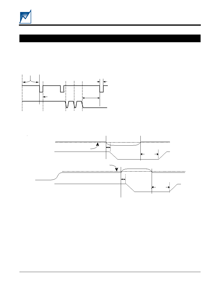
Figure 8 - START and STOP Conditions
Table 9. Slave Addresses
START and STOP Conditions
When both the data and clock lines are high the bus is said
to be not busy. A high-to-low transition on the data line,
while the clock is high, is defined as the Start condition.
A low-to-high transition on the data line, while the clock
is high, is defined as the Stop condition. See Figure 8.
Acknowledge (ACK)
Acknowledge is a software convention used to indicate
successful data transfers. The transmitting device,
either the Master or the Slave, will release the bus after
transmitting eight bits. During the ninth clock cycle the
receiver will pull the SDA line low to Acknowledge that it
received the eight bits of data. The Master will leave the
SDA line high (NACK) when it terminates a read function.
The SMS46 will respond with an Acknowledge after recog-
nition of a Start condition and its slave address byte. If both
the device and a write operation are selected the SMS46
will respond with an Acknowledge after the receipt of each
subsequent 8-Bit word. In the READ mode the SMS46
transmits eight bits of data, then releases the SDA line, and
monitors the line for an Acknowledge signal. If an Acknowl-
edge is detected and no Stop condition is generated by the
Master, the SMS46 will continue to transmit data. If a
NACK is detected the SMS46 will terminate further data
transmissions and await a Stop condition before returning
to the standby power mode.
Device Addressing
Following a Start condition the Master must output the
address of the Slave it is accessing. The most significant
four bits of the Slave address are the device type
identifier/address. For the SMS46 the default is 1010
BIN
.
The next two bits are the Bus Address. The next bit (the
7th) is the MSB of the memory address.
Read/Write Bit
The last bit of the data stream defines the operation to be
performed. When set to 1 a Read operation is selected;
when set to 0 a Write operation is selected.
WRITE OPERATIONS
The SMS46 allows two types of Write operations: byte
Write and page Write. A byte Write operation writes a
single byte during the nonvolatile write period (t
WR
). The
page Write operation, limited to the memory array, allows
up to 16 bytes in the same page to be written during t
WR
.
Byte Write
After the Slave address is sent (to identify the Slave
device and select either a Read or Write operation), a
second byte is transmitted which contains the low order
8 bit address of any one of the 512 words in the array.
Upon receipt of the word address the SMS46 responds with
an Acknowledge. After receiving the next byte of data it
again responds with an Acknowledge. The Master then
terminates the transfer by generating a Stop condition, at
which time the SMS46 begins the internal Write cycle.
While the internal Write cycle is in progress the SMS46
inputs are disabled and the device will not respond to any
requests from the Master.
Page Write (memory only)
The SMS46 is capable of a 16-byte page Write operation.
It is initiated in the same manner as the byte Write
operation, but instead of terminating the Write cycle after
the first data word the Master can transmit up to 15 more
bytes of data. After the receipt of each byte the SMS46 will
respond with an Acknowledge.
The SMS46 automatically increments the address for
subsequent data words. After the receipt of each word the
low order address bits are internally incremented by one.
2047 Fig10
SCL
SDA In
START
Condition
STOP
Condition
7
D
B
S
M
6
D
5
D
4
D
3
D
2
D
1
D
0
D
B
S
L
s
t
i
B
s
s
e
r
d
d
A
e
p
y
T
e
c
i
v
e
D
s
u
B
B
S
M
W
/
R
6
4
S
M
S
x
x
x
x
1
0
0
1
r
e
t
s
i
g
e
R
n
o
i
t
a
r
u
g
i
f
n
o
C
1
0
1
0
)
t
l
u
a
f
e
d
(
y
r
o
m
e
M
1
0
1
1
y
r
o
m
e
M
e
t
a
n
r
e
t
l
A
I
2
C INTERFACE (CONTINUED)
13
2083 1.1 06/04/04
SMS46
SUMMIT MICROELECTRONICS, Inc.
Preliminary Information
Figure 9 - Read and Write Operations
The high order bits of the address byte remain constant.
Should the Master transmit more than 16 bytes, prior to
generating the Stop condition, the address counter will
rollover and the previously written data will be overwrit-
ten. As with the byte Write operation, all inputs are disabled
during the internal Write cycle. Refer to Figure 11 for the
address, Acknowledge, and data transfer sequence.
N
A
C
K
N
A
C
K
Typical Write Operation
(Standard memory device type)
S
T
A
R
T
A
C
K
B
A
2
B
A
1
A
8
R
/
W
A
C
K
D
7
D
6
D
5
D
4
D
3
D
2
D
1
D
0
A
C
K
S
T
O
P
Master
SDA
Slave
0
1
1 0
A
C
K
R
/
W
A
C
K
D
7
D
6
D
5
D
4
D
3
D
2
D
1
D
0
A
C
K
S
T
O
P
S
T
A
R
T
Writing Configuration Registers
Master
SDA
Slave
0 1
1 0
Master
SDA
Slave
Device Type
Address
Bus
Address
A
7
A
6
A
5
A
4
A
3
A
2
A
1
A
0
C
7
C
6
C
5
C
4
C
3
C
2
C
1
C
0
A
C
K
R
/
W
A
C
K
S
T
A
R
T
C
7
C
6
C
5
C
4
C
3
C
2
C
1
C
0
Reading the Configuration Register
0 1
1 0
A
C
K
R
/
W
S
T
O
P
S
T
A
R
T
D
7
D
6
D
5
D
4
D
3
D
2
D
1
D
0
0 1
1 0
Up to 15
additional bytes
can be written
before issuing
the stop.
B
A
2
B
A
1
X
B
A
2
B
A
1
X
B
A
2
B
A
1
X
2047 Fig11
Typical Reading Operation
(Alternate memory device type)
Master
SDA
Slave
A
C
K
R
/
W
A
C
K
S
T
A
R
T
A
7
A
6
A
5
A
4
A
3
A
2
A
1
A
0
1 1
1 0
A
C
K
R
/
W
S
T
O
P
S
T
A
R
T
D
7
D
6
D
5
D
4
D
3
D
2
D
1
D
0
1 1
1 0
B
A
2
B
A
1
A
8
B
A
2
B
A
1
A
8
I
2
C INTERFACE (CONTINUED)
14
SMS46
2083 1.1 06/04/04
SUMMIT MICROELECTRONICS, Inc.
Preliminary Information
Figure 10 - Write Flow Chart
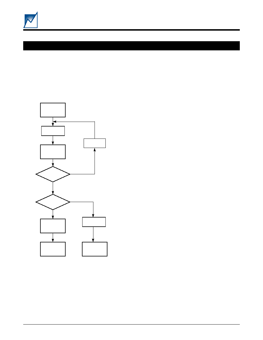
Acknowledge Polling
When the SMS46 is performing an internal Write operation
it will ignore any new Start conditions. Since the device will
only return an acknowledge after it accepts the Start the
part can be continuously queried until an acknowledge is
issued, indicating that the internal Write cycle is complete.
See the flow chart for the proper sequence of operations for
polling.
READ OPERATIONS
Read operations are initiated with the R/W bit of the
identification field set to 1. There are two different Read
options: 1. Current Address Byte Read, and 2. Random
Address Byte Read.
Current Address Read (memory only)
The SMS46 contains an internal address counter which
maintains the address of the last word accessed, incre-
mented by one. If the last address accessed (either a
Read or Write) was to address location n, the next Read
operation would access data from address location n+1
and increment the current address pointer. When the
SMS46 receives the Slave address field with the R/W bit
set to 1 it issues an acknowledge and transmits the 8-Bit
word stored at address location n+1. The current address
byte Read operation only accesses a single byte of data.
The Master sets the SDA line to NACK and generates a
stop condition. At this point the SMS46 discontinues data
transmission.
Random Address Read (Register and Memory)
Random address Read operations allow the Master to
access any memory location in a random fashion. This
operation involves a two-step process. First, the Master
issues a write command which includes the start condi-
tion and the Slave address field (with the R/W bit set to
Write), followed by the address of the word it is to Read.
This procedure sets the internal address counter of the
SMS46 to the desired address. After the word address
acknowledge is received by the Master it immediately
reissues a Start condition, followed by another Slave
address field with the R/W bit set to READ. The SMS46 will
respond with an Acknowledge and then transmit the 8 data
bits stored at the addressed location. At this point the
Master sets the SDA line to NACK and generates a Stop
condition. The SMS46 discontinues data transmission and
reverts to its standby power mode.
Sequential READ (Memory Only)
Sequential Reads can be initiated as either a current
address Read or random access Read. The first word is
transmitted as with the other byte Read modes (current
address byte Read or random address byte Read);
however, the Master now responds with an Acknowledge,
indicating that it requires additional data from the SMS46.
The SMS46 continues to output data for each Acknowl-
edge received. The Master terminates the sequential
Read operation by responding with a NACK, and issues
a Stop condition. During a sequential Read operation the
internal address counter is automatically incremented
with each Acknowledge signal. For Read operations all
address bits are incremented, allowing the entire array to
be read using a single Read command. After a count of
the last memory address the address counter will rollover
and the memory will continue to output data.
Next
Operation
a Write?
ACK
Returned
Issue
Address
Proceed
With
Write
Await
Next
Command
Issue Stop
Issue Slave
Address and
R/W = 0
Issue Stop
Write Cycle
In Progress
Yes
No
Issue Start
2047 Fig12
Yes
No
I
2
C INTERFACE (CONTINUED)
15
2083 1.1 06/04/04
SMS46
SUMMIT MICROELECTRONICS, Inc.
Preliminary Information
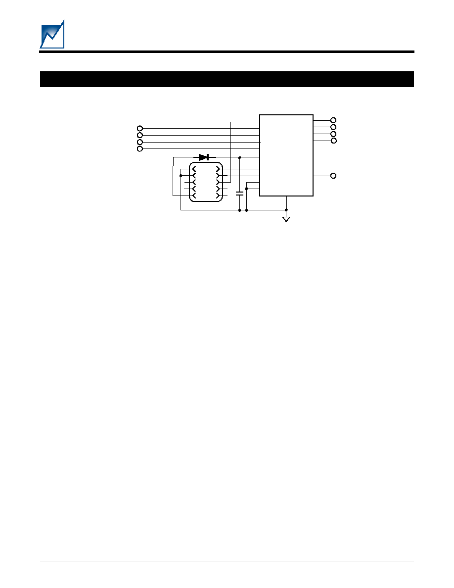
APPLICATIONS
Figure 11 - Application Schematic
NOTES:
1. C1 is a 0.1µF.
2. Connector J1 is an SMX3200 (see Figure 6).
3. D1 is a 1N4148
SMS46
2
4
6
8
10
1
3
5
7
9
MR#
V0
V1
V2
V3
WLDI
RESET#0
RESET#1
RESET#2
SCL
SDA
A1
A2
GND
1
16
2
3
14
10
9
6
7
11
4
5
13
8
J1
C1
V0
V1
V2
V3
2047 Fig13
VDD_CAP
12
15
RESET#3
D1
16
SMS46
2083 1.1 06/04/04
SUMMIT MICROELECTRONICS, Inc.
Preliminary Information
PACKAGE
16 PIN SSOP PACKAGE
0.007 - 0.010
(0.18 - 0.25)
0.150 - 0.157
(3.81 - 3.99)
0.025
(0.635)
0.016 - 0.050
(0.41 - 1.27)
0.008 - 0.012
(0.20 - 0.31)
0.189 - 0.197
(4.80 - 5.00)
0.228 - 0.244
(5.79 - 6.20)
Pin 1
0.004 - 0.010
(0.10 - 0.25)
0.059
(1.50)
0.053 - 0.069
(1.35 - 1.75)
MAX
16 Pin SSOP
Ref. JEDEC MO-137
Inches
(Millimeters)
0" Min to
8" Max
DEFAULT CONFIGURATION REGISTER SETTINGS - SMS46GC-238
The default device ordering number is SMS46GC-238, is programmed as described above and tested
over the commercial temperature range.
R egister C ontents
Function
R 00
56
V0 threshold set to 3.090V
R 01 28
V1 threshold set to 2.400V
R 02 A0
V2 threshold set to 1.400V
R 03 14
V3 threshold set to 0.700V
R 04 F3
R eset T rigger source set for all channels, V0, V 1 set to high range and V2, V 3
set to low range
R 05 X 0
U pper bits are volatile status indication of input supply condition. V 0, V1, V2
and V3 set to m onitor U V U nder Voltage.
R 06 C 5
R eset tim eout set to 100m s, W atchdog T im er set to 1.6s. B its D 4 and D 3
indicate revision control.
R 07 40
EE m em ory slave address is 1011, C onfiguration registers are unlocked.
17
2083 1.1 06/04/04
SMS46
SUMMIT MICROELECTRONICS, Inc.
Preliminary Information
NOTICE
NOTE 1 - This is a Preliminary Information data sheet that describes a Summit product currently in pre-production with limited
characterization.
SUMMIT Microelectronics, Inc. reserves the right to make changes to the products contained in this publication in order to improve design,
performance or reliability. SUMMIT Microelectronics, Inc. assumes no responsibility for the use of any circuits described herein, conveys no license
under any patent or other right, and makes no representation that the circuits are free of patent infringement. Charts and schedules contained
herein reflect representative operating parameters, and may vary depending upon a user's specific application. While the information in this
publication has been carefully checked, SUMMIT Microelectronics, Inc. shall not be liable for any damages arising as a result of any error or omission.
SUMMIT Microelectronics, Inc. does not recommend the use of any of its products in life support or aviation applications where the failure or
malfunction of the product can reasonably be expected to cause any failure of either system or to significantly affect their safety or effectiveness.
Products are not authorized for use in such applications unless SUMMIT Microelectronics, Inc. receives written assurances, to its satisfaction,
that: (a) the risk of injury or damage has been minimized; (b) the user assumes all such risks; and (c) potential liability of SUMMIT Microelectronics,
Inc. is adequately protected under the circumstances.
Revision 1.1 - This document supersedes all previous versions. Please check the Summit Microelectronics, Inc. web site at
www.summitmicro.com
for data sheet updates.
© Copyright 2004 SUMMIT MICROELECTRONICS, Inc.
PROGRAMMABLE ANALOG FOR A DIGITAL WORLDTM
I2C is a trademark of Philips Corporation.
ORDERING INFORMATION
S M S 4 6
G
n n n
P a c k a g e
G = 1 6 L e a d S S O P
P a r t N u m b e r S u f f i x ( s e e p a g e 1 7 )
S u m m i t P a r t
N u m b e r
S p e c if ic r e q u ir e m e n t s a r e c o n t a in e d in t h e
s u f f ix s u c h a s H e x c o d e , H e x c o d e r e v is io n , e t c .
C
T e m p R a n g e
C = C o m m e r c ia l
B la n k = I n d u s t r ia l
SMS46G
AYYWW
Pin 1
Identifier
Annn
Summit Part Number
Date Code (YYWW)
Part Number suffix
(Contains Customer specific ordering requirements)
Lot tracking code (Summit use)
Drawing not to scale
xx
Status Tracking Code
(Blank, MS, ES, 01, 02,...)
(Summit Use)
Product Tracking Code (Summit use)
SUMMIT
PART MARKING