 | –≠–ª–µ–∫—Ç—Ä–æ–Ω–Ω—ã–π –∫–æ–º–ø–æ–Ω–µ–Ω—Ç: SMS66FR10 | –°–∫–∞—á–∞—Ç—å:  PDF PDF  ZIP ZIP |
SMS66
Preliminary Information
1
(See Last Page)
© SUMMIT Microelectronics, Inc. 2003 ∑
300 Orchard City Drive, #131 ∑ Campbell CA 95006
∑ Phone 408 378-6461 ∑ FAX 408 378-6596 www.summitmicro.com
2070 1.0 7/16/03
1
Six-Channel Power Supply Supervisor and Cacsade Sequence Controller
FEATURES & APPLICATIONS
∑ Very accurate monitor function ≠ 5mV steps
∑ Monitors and sequences up to six supplies
∑ Programmable Power-on/-off sequencing
∑ Monitors internal temperature sensor
∑ Operates from 12V or 3.3V supply
∑ Monitors 12V input and VDD
∑ Monitors two general-purpose 10-bit ADC inputs
∑ Programmable threshold limits (2 OV/2 UV) for
each monitored input
∑ Programmable RESET, HEALTHY and FAULT
functions
∑ 4k-bit general purpose nonvolatile memory
∑ I
2
C 2-wire serial bus for programming
configuration and monitoring status, including
10-bit ADC conversion results
Applications
∑ Monitor and Sequence Distributed Power and
Point of Load Power Supplies
∑ Multi-voltage Processors, DSPs, ASICs used in
Telecom, CompactPCI or server systems
INTRODUCTION
The SMS66 is a very accurate programmable power
supply supervisor that monitors and sequences. It
controls sequencing time and position of up to six
isolated or non-isolated distributed or POL DC/DC
converters. The monitor supervisory function has two
independent UV and OV settings for each supply and
can be set in 5mV steps. The SMS66 also sequences
the power supplies in any order using enable outputs
with programmable polarity.
The SMS66 monitors six power supply channels as
well as VDD, 12V input, two general-purpose analog
inputs and an internal temperature sensor using a 10-
bit ADC. The 10-bit ADC can measure the value on
any one of the input channels and output the
conversion data via the I
2
C bus.
Using the I
2
C interface, a host system can
communicate with the SMS66 status register,
optionally control Power-on/off, and utilize 4 K-bits of
nonvolatile memory.
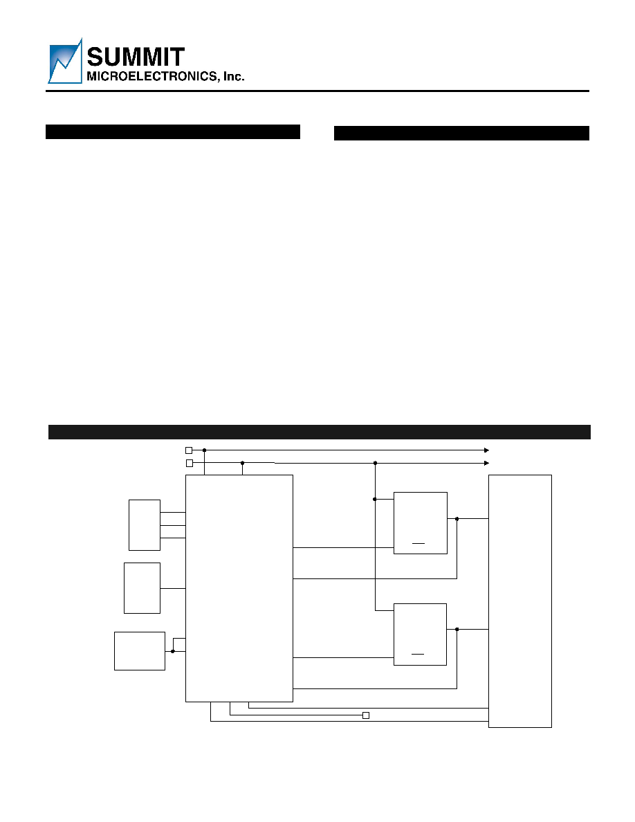
SIMPLIFIED APPLICATIONS DRAWING
PUP
F
VM
F
PUP
A
VM
A
SMS66
µP/
DSP/
NPU/
FPGA
VDD
RS
T
HE
ALTHY
MR
VDD (+2.7V to +5.5V Range)
RESET
DONE
HEALTHY
12V
IN
12VIN (+8V to +15V Range)
External
or
Internal
TEMP
SENSOR
AIN1
VREF_ADC
2.5VIN
1.2VIN
12V
SDA
SCL
I
2
C
BUS
3.3V
A2
VREF_OUT
VIN
Vout
DC/DC
Converter A
ON/OFF
VIN
Vout
DC/DC
Converter F
ON/OFF
External or
Internal
REFERENCE
Figure 1 ≠ Applications Schematic using the SMS66 Controller to cascade sequence up to six DC/DC
Converters while also providing supervisory functions.
Note: This is an applications example only. Some pins, components and values are not shown.
SMS66
Preliminary Information
Summit Microelectronics, Inc
2070 1.0 7/16/03
2
GENERAL DESCRIPTION
The SMS66 is a highly integrated power supply
controller, monitor and sequencer. It has the ability to
control, monitor and sequence up to six power
supplies. Also, the SMS66 can monitor the VDD input,
the 12V input, two general-purpose analog inputs and
the internal temperature sensor. The SMS66 has
three operating modes: Power-on sequencing mode,
monitor mode, and Power-off sequencing mode.
Power-on sequencing can be initiated via the
PWR_ON/OFF pin or I
2
C control. In this mode, the
SMS66 will sequence the power supply channels on in
any order by activating the PUP outputs and
monitoring the respective converter voltages to ensure
cascading of the supplies. A programmable sequence
termination timer can be set to disable all channels if
the Power-on sequence stalls. During this mode the
HEALTHY output will remain inactive and the RST
output will remain active.
Once the Power-on sequencing mode is complete, the
SMS66 enters monitor mode. In the monitor mode the
SMS66 supervises the supplies to within 5mV, and
enables the triggering of outputs by monitored fault
conditions.
The 10-bit ADC cycles through all 11 channels every
2ms and checks the conversions against the
programmed threshold limits. The results can be used
to trigger RST, HEALTHY and FAULT outputs as well
as to trigger a Power-off or a Force Shutdown
operation.
The Power-off sequencing mode can only be entered
while the SMS66 is in the monitoring mode. It can be
initiated by either bringing the PWR_ON/OFF pin
inactive, through I
2
C control or triggered by a channel
exceeding its programmed thresholds. Once Power-
off is initiated it will disable the Active DC Control and
sequence the PUP outputs off in either the same or
reverse order as Power-on sequencing and monitor
the supply voltages to ensure cascading of the
supplies as they turn off. The sequence termination
timer can be programmed to immediately disable all
channels if the Power-off sequencing stalls. The RST
output will remain active throughout this mode while
the HEALTHY output remains inactive.
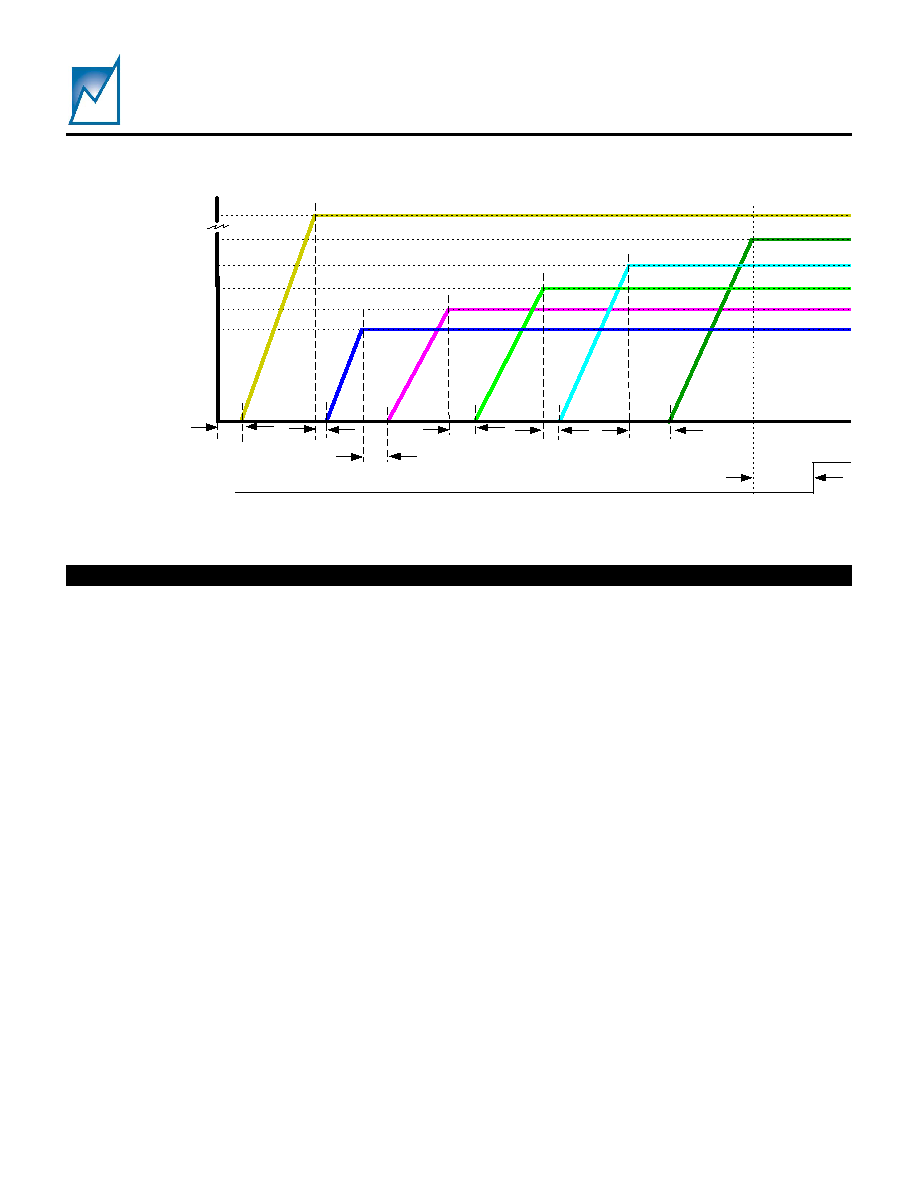
Figure 2 ≠ Example Power Supply Sequencing and System Start-up Initialization using the SMS66.
Any order of supply sequencing can be applied using the SMS66 with very accurate monitoring and
supervisory functions.
2.5V
2.7V
1.8V
2.0V
1.5V
VDD (+2.7V to +5.5V)
or 12VIN ( +8V to +15V)
RST#
t
PRTO
t
DPONC
t
DPONB
t
DPOND
t
DPONE
t
DPONF
t
DPONA
SMS66
Preliminary Information
Summit Microelectronics, Inc
2070 1.0 7/16/03
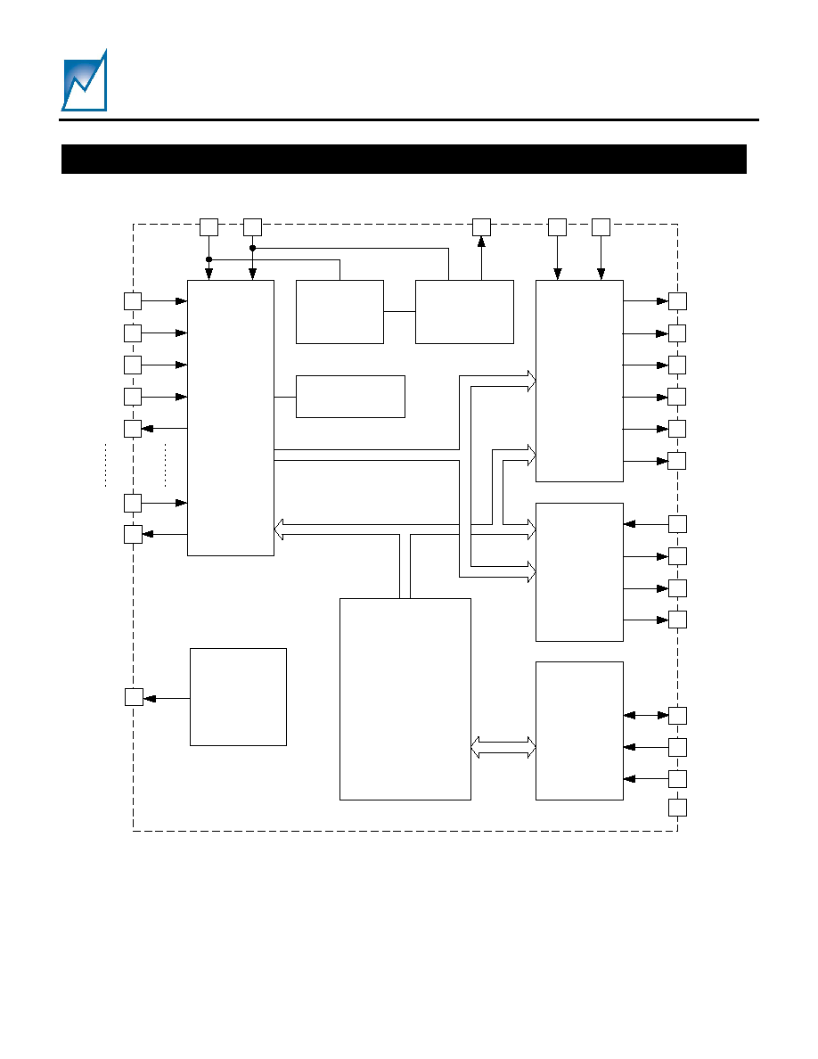
3
AIN
2
10-Bit ADC
VREF_ADC
AIN
1
VM
A
CAP
A
VM
F
CAP
F
VREF_OUT
12VIN
VDD
PUP
A
Sequence
Control
PUP
B
PUP
C
PUP
D
PUP
E
PUP
F
FS
PWR_ON/OFF
3.6V or
5.5V
Regulator
Power
Supply
Arbitrator
Temperature
Sensor
VDD_CAP
Output
Control
MR
RST
HEALTHY
FAULT
Memory and
Limit Registers
I
2
C
Interface
SDA
SCL
A2
GND
Reference
Figure 3 ≠SMS66 Internal Functional Block Diagram.
INTERNAL FUNCTIONAL BLOCK DIAGRAM
SMS66
Preliminary Information
Summit Microelectronics, Inc
2070 1.0 7/16/03
4
Pin
Number
Pin
Type
Pin Name
Pin Description
1
DATA SDA I
2
C Bi-directional data line
2
CLK SCL I
2
C Clock line
3
IN A2
The address pin is biased either to VDD_CAP or GND. When
communicating with the SMS66 over the 2-wire bus A2 provides a
mechanism for assigning a unique bus address.
4
IN MR
Programmable active high/low input. When asserted the RST output will be
go active. When de-asserted the RST output will go inactive immediately
after a reset timeout period (t
PRTO
) if there are no RST trigger sources active.
This timeout period makes it suitable to use a pushbutton for manual reset.
5
IN PWR_ON/OFF
Programmable active high/low input signals the start of the power
sequencing. When asserted the part will sequence the supplies on and
when de-asserted the part will sequence the supplies off.
6
IN FS
Programmable active high/low input. Force shutdown is used to immediately
turn off all converter enable signals (PUP outputs)
7
OUT FAULT
Programmable active high/low open drain Fault output. Active when a
programmed fault condition exists on AIN1, AIN2, or the internal temperature
sensor.
8
OUT HEALTHY
Programmable active high/low open drain Healthy output. Active when all
programmed power supply inputs and monitored inputs are within OV and
UV limits.
9
OUT RST
Programmable active high/low open drain Reset output. Active when a
programmed fault condition exists on any power supply inputs or monitored
inputs or when MR is active. RST has a programmable timeout period with
options for 0.64ms, 25ms, 100ms and 200ms.
10
IN AIN1
General purpose monitored analog input
11
IN AIN2
General purpose monitored analog input
12, 44,
39, 34,
29, 24,
19
GND GND Ground
13
IN VREF_ADC
Voltage reference input used for A/D conversion where:
(4XVREF_ADC) = Full Scale for VM
A-F
and VDD
(12XVREF_ADC) = FS for 12VIN
(2XVREF_ADC) = FS for AIN1 and AIN2.
VREF_ADC can be connected to VREF_CNTL in most applications.
14
O VREF_OUT
Voltage reference output for the internal 1.25V reference.
41,36,
31,26,
21,16
IN VM
X
Monitored voltage input, VM
A
through VM
F
PIN DESCRIPTIONS
SMS66
Preliminary Information
Summit Microelectronics, Inc
2070 1.0 7/16/03
5
Pin
Number
Pin
Type
Pin Name
Pin Description
42,37,
32,27,
22,17
CAP CAP
X
External capacitor input used to filter the VM
X
inputs to the 10-bit ADC, CAP
A
through CAP
F
. This provides an RC filter where R = 25k.
43,38,
33,28,
23,18
OUT PUP
X
Programmable active high/low open drain converter enable output, PUP
A
through PUP
F
45, 40,
35, 30,
25, 20,
15
NC NC
No Connection
46
PWR VDD Power supply of the part
47
PWR 12VIN 12V power supply input internally regulated to either 3.6V or 5.5V
48
CAP VDD_CAP External capacitor input used to filter the internal supply
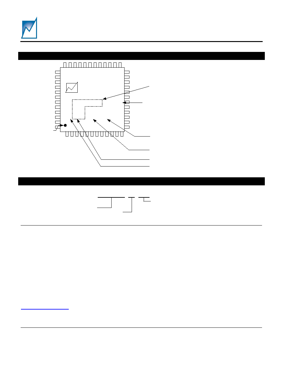
PACKAGE AND PIN CONFIGURATION
48 LEAD TQFP
1
2
3
4
5
6
7
8
9
10
11
12
13
14
15
16
17
18
19
20
21
22
23
24
36
35
34
33
32
31
30
29
28
27
26
25
48
47
46
45
44
43
42
41
40
39
38
37
SDA
SCL
A2
MR
PWR_ON/OFF
FS
FAULT
RST
HEALTHY
AIN1
GND
AIN2
VMB
NC
GND
PUPC
CAPC
VMC
NC
GND
PUPD
CAPD
NC
VMD
V
DD_CAP
12VI
N
VDD
NC
GN
D
PU
P
A
CAPA
VM
A
NC
GN
D
CAP
B
PU
P
B
VRE
F
_ADC
VR
E
F
_
O
U
T
NC
VMF
CAPF
PU
PF
GN
D
NC
VME
CA
P
E
GN
D
PUP
E
PIN DESCRIPTIONS (Cont.)
SMS66
Preliminary Information
Summit Microelectronics, Inc
2070 1.0 7/16/03
6
ABSOLUTE MAXIMUM RATINGS
Temperature Under Bias ...................... -55
∞
C to 125
∞
C
Storage Temperature............................ -65
∞
C to 150
∞
C
Terminal Voltage with Respect to GND:
VDD Supply Voltage ..........................-0.3V to 6.0V
12VIN Supply Voltage......................-0.3V to 15.0V
All Others ................................-0.3V to V
DD
+ 0.7V
Output Short Circuit Current ............................... 100mA
Lead Solder Temperature (10 secs).................... 300
∞
C
Note - The device is not guaranteed to function outside its operating
rating. Stresses listed under Absolute Maximum Ratings may cause
permanent damage to the device. These are stress ratings only and
functional operation of the device at these or any other conditions
outside those listed in the operational sections of the specification is
not implied. Exposure to any absolute maximum rating for extended
periods may affect device performance and reliability. Devices are
ESD sensitive. Handling precautions are recommended.
RECOMMENDED OPERATING CONDITIONS
Temperature Range (Industrial)...........≠40
∞
C to +85
∞
C
(Commercial) ............≠5
∞
C to +70
∞
C
VDD Supply Voltage .................................. 2.7V to 5.5V
EEPROM Write Supply Voltage
1
..............3.0V to 5.5V
12VIN Supply Voltage
2
............................ 8.0V to 15.0V
VIN ............................................................ GND to VDD
VOUT ...................................................... GND to 15.0V
Package Thermal Resistance (
JA
)
48 Lead TQFP........................................80
o
C/W
Moisture Classification Level 1 (MSL 1) per J-STD- 020
Note 1 ≠ During an EEPROM memory array or Configuration
Register Write, the supply voltage minimum is 3.0V.
Note 2 ≠ Range depends on internal regulator set to 3.6V or 5.5V.
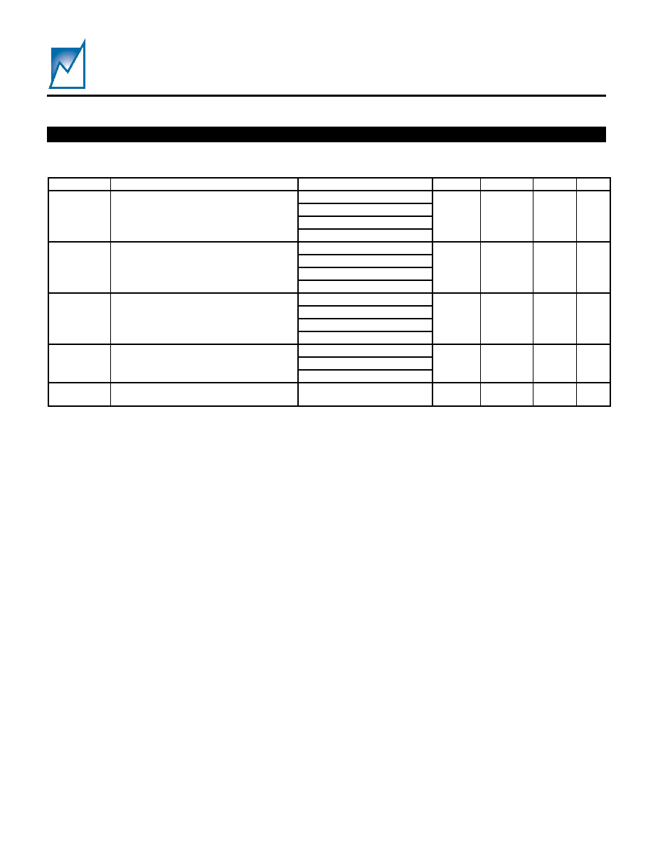
DC OPERATING CHARACTERISTICS
(Over recommended operating conditions, unless otherwise noted. All voltages are relative to GND.)
Symbol
Parameter
Notes
Min.
Typ.
Max
Unit
VDD
Low Range Supply Voltage
Note 1
2.7
5.5
V
Note 2. Internally
regulated to 5.5V
10 15
V
12VIN
High Range Supply Voltage
Note 2. Internally
regulated to 3.6V
7 14
I
DD
Power Supply Current from
VDD
12VIN floating
3
5
mA
I
12VIN
Power Supply Current from
12VIN
VDD floating
3
5
mA
PT
OV1
Programmable Threshold for
OV1 condition
0
4XV
REF
V
PT
OV2
Programmable Threshold for
OV2 condition
0
4XV
REF
V
PT
OV1ACC
Programmable UV Threshold
Accuracy
-0.005
PT
UV
+0.005 V
PT
OV2ACC
Programmable OV Threshold
Accuracy
-0.005
PT
OV
+0.005 V
PT
UV1
Programmable Threshold for
UV1 condition
0
4XV
REF
V
PT
UV2
Programmable Threshold for
UV2 condition
0
4XV
REF
V
PT
UV1ACC
Programmable UV1
Threshold Accuracy
-0.005
PT
UV1
+0.005 V
PT
UV2ACC
Programmable UV2
Threshold Accuracy
-0.005
PT
UV2
+0.005 V
Note 1 ≠ During an EEPROM memory array or Configuration Register Write, the supply voltage minimum is 3.0V.
Note 2 ≠ Range depends on internal regulator set to 3.6V or 5.5V.
SMS66
Preliminary Information
Summit Microelectronics, Inc
2070 1.0 7/16/03
7
DC OPERATING CHARACTERISTICS (CONTINUED)
(Over recommended operating conditions, unless otherwise noted. All voltages are relative to GND.)
Symbol Parameter
Notes Min
Typ
Max
Unit
PUP characteristics
V
OL
Output Low Voltage
I
SINK
= 2mA
0
0.4
V
All other input and output characteristics
VDD = 2.7V
0.9xVDD
VDD
V
V
IH
Input High Voltage
(FS,PWR_ON/OFF, MR#)
VDD = 5.0V
0.7xVDD
VDD
V
VDD = 2.7V
-0.1
0.1xVDD
V
V
IL
Input Low Voltage (FS,
PWR_ON/OFF, MR#)
VDD = 5.0V
-0.1
0.3xVDD
V
V
OL
Programmable Open Drain
Outputs (RST, HEALTHY,
FAULT)
I
SINK
= 2mA
0
0.4
V
I
OL
Output Low Current
Note ≠ Total I
SINK
from all PUPx pins
should not exceed 3mA or accuracy
specifications will be affected
0 1.0
mA
VM
Monitor
VM Monitor Threshold Step Size
VM pins
5
mV
VA
Monitor
AINx Monitor Threshold Step Size AIN1/AIN2 pins
2.5
mV
T
Monitor
Temperature Threshold Step Size Internal Temp Sensor
0.25
o
C
V
REF_OUT
Internal 1.25V
REF
Output Voltage
1.24
1.25
1.26
V
≠40
∞
C to +85
∞
C
-0.25 +0.25
%
V
REF
TC
Internal V
REF
Temperature
Coefficient
≠5
∞
C to +70
∞
C
-0.15 +0.15
%
V
REF
ACC Internal V
REF
Accuracy
-0.4
+0.4
%
External
V
REF
External V
REF
Voltage Range
0.5
VDD_CAP
V
SMS66
Preliminary Information
Summit Microelectronics, Inc
2070 1.0 7/16/03
8
DC OPERATING CHARACTERISTICS (CONTINUED)
(Over recommended operating conditions, unless otherwise noted. All voltages are relative to GND.)
Symbol Parameter
Notes Min
Typ
Max
Unit
AIN1/AIN2 ADC characteristics
N Resolution
10
Bits
MC Missing
Codes
Minimum resolution for which no
missing codes are guaranteed
10
Bits
S/N Signal-to-Noise
Ratio
Conversion rate = 500Hz
72 db
DNL Differential
Non-Linearity
-1/2 +1/2
LSB
INL Integral
Non-Linearity
-1 +1
LSB
GAIN
Positive full scale gain error
-0.5 +0.5
%
Offset Offset
Error
-1 +1
LSB
ZSE
Zero Scale Error
-1 +1
LSB
FSE
Full Scale Error
-1 +1
LSB
ADC_TC
Full Scale Temperature
Coefficient
±15
PPM
/
o
C
IM
ADC
Analog ADC Input Impedance
AIN1, AIN2
10
M
II
VREF_ADC
V
REF_ADC
Input Current
250
nA
IC
VREF_ADC
V
REF_ADC
Input Capacitance
200
pF
IR
VREF_ADC
V
REF_ADC
Input Impedance
1
k
SMS66
Preliminary Information
Summit Microelectronics, Inc
2070 1.0 7/16/03
9
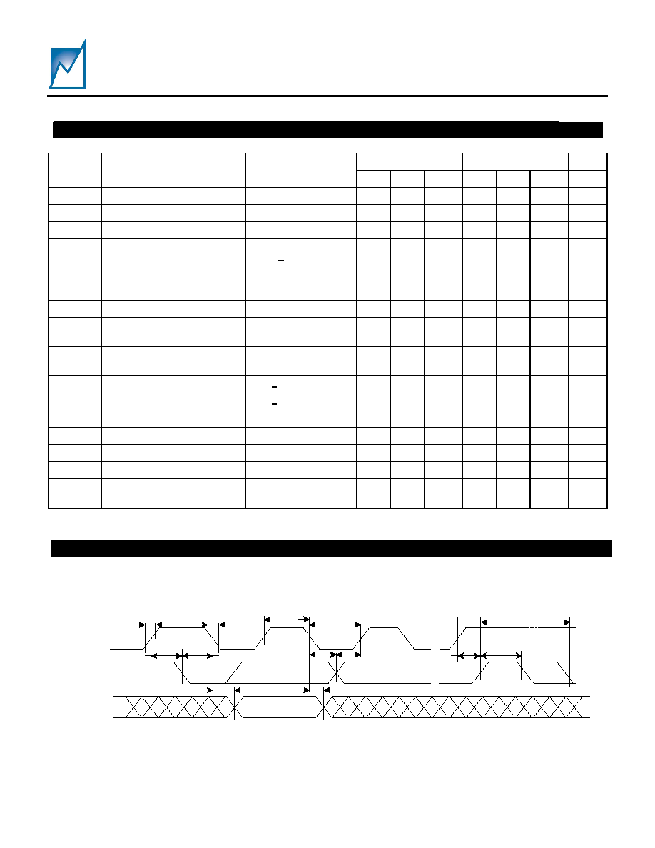
AC OPERATING CHARACTERISTICS
Over recommended operating conditions, unless otherwise noted. All voltages are relative to GND. See Figure 4B and 4C Timing
diagrams.
Symbol Description
Conditions
Min
Typ
Max
Unit
0.64ms
12.5ms
25ms
t
DPON
Programmable Power-on delay from
VM
X
out-of-fault to PUP
Y
active
50ms
-15 t
DPON
+15 %
0.64ms
12.5ms
25ms
t
DPOFF
Programmable Power-off delay from
VM
X
off to PUP
Y
inactive
50ms
-15 t
DPOFF
+15 %
0.64ms
25ms
100ms
t
PRTO
Programmable Reset Time-Out
Period
200ms
-15 t
PRTO
+15 %
100ms
200ms
t
STT
Programmable Sequence
Termination Timer
400ms
-15 t
STT
+15
%
t
ADC
10-bit ADC sampling period
Time for all 11 channels
2
ms
SMS66
Preliminary Information
Summit Microelectronics, Inc
2070 1.0 7/16/03
10
I
2
C 2-WIRE SERIAL INTERFACE AC OPERATING
CHARACTERISTICS - 100/400kHz
Over recommended operating conditions, unless otherwise noted. All voltages are relative to GND. See Figure 4A Timing Diagram.
100kHz 400kHz
Symbol Description
Conditions
Min Typ Max Min Typ Max Units
f
SCL
SCL Clock Frequency
0 100
0 400
KHz
t
LOW
Clock Low Period
4.7 1.3 µs
t
HIGH
Clock
High
Period
4.0 0.6 µs
t
BUF
Bus Free Time
Before New Transmission
-
Note 1/
4.7 1.3 µs
t
SU:STA
Start Condition Setup Time
4.7
0.6
µs
t
HD:STA
Start Condition Hold Time
4.0
0.6
µs
t
SU:STO
Stop Condition Setup Time
4.0
0.6
µs
t
AA
Clock Edge to Data Valid
SCL low to valid
SDA (cycle n)
0.2 3.5 0.2 0.9 µs
t
DH
Data Output Hold Time
SCL low (cycle n+1)
to SDA change
0.2 0.2 µs
t
R
SCL and SDA Rise Time
Note 1/
1000
1000
ns
t
F
SCL and SDA Fall Time
Note 1/
300 300 ns
t
SU:DAT
Data In Setup Time
250
150
ns
t
HD:DAT
Data In Hold Time
0
0
ns
TI
Noise Filter SCL and SDA
Noise suppression
100
100
ns
t
WR
Write
Cycle
Time
Memory
Array
5 5 ms
t
WR
Write
Cycle
Time
Configuration
Registers
10 10
ms
Note: 1/ - Guaranteed by Design.
t
R
t
F
t
HIGH
t
LOW
t
SU:SDA
t
HD:SDA
t
SU:DAT
t
HD:DAT
t
SU:STO
t
BUF
t
DH
t
AA
SCL
SDA
(IN)
SDA
(OUT)
t
W R (For W rite Operation Only)
Figure 4A . Basic I
2
C Serial Interface Timing
TIMING DIAGRAMS
SMS66
Preliminary Information
Summit Microelectronics, Inc
2070 1.0 7/16/03
11
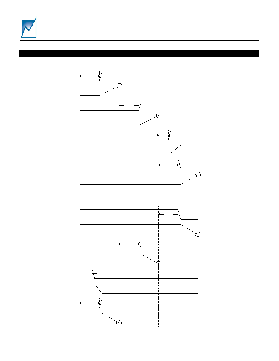
Figure 4B - The SMS66 sequencing the supplies on and then monitoring for fault conditions.
Figure 4C - The SMS66 sequencing the supplies off.
t
DPONA
t
DPONB
t
DPONC
t
DPOND
0
1
2
VM
A
PUP
A
PUP
B
PUP
C
PUP
D
VM
B
VM
C
VM
D
TIMING DIAGRAMS (CONTINUED)
t
DPOFFA
t
DPOFFB
t
DPOFFC
t
DPOFFD
2
1
0
VM
A
PUP
A
PUP
B
PUP
C
PUP
D
VM
B
VM
C
VM
D

SMS66
Preliminary Information
Summit Microelectronics, Inc
2070 1.0 7/16/03
12
APPLICATIONS INFORMATION
DEVICE OPERATION
POWER SUPPLY
The SMS66 can be powered by either a 12V input
through the 12VIN pin or by a 3.3V or 5.0V input
through the VDD pin. The 12VIN pin feeds an internal
programmable regulator that internally generates
either 5.5V or 3.6V. A voltage arbitration circuit allows
the device to be powered by the highest voltage from
either the regulator output or the VDD input. This
voltage arbitration circuit continuously checks for these
voltages to determine which will power the SMS66.
The resultant internal power supply rail is connected to
the VDD_CAP pin that allows both filtering and hold-
up of the internal power supply.
MODES OF OPERATION
The SMS66 has three basic modes of operation:
Power-on sequencing mode, monitoring mode, and
Power-off sequencing mode (shown in Figures 4B
through 4E). In addition, there is a forced shutdown
feature. A detailed description of each mode and
feature follows.
POWER-ON SEQUENCING
The SMS66 can be programmed to sequence up to six
power supplies in any order. Each of these six
channels (A-F) has an associated open drain PUP
output that, when connected to a converter's enable
pin, controls the turn-on of the converter. The
channels are assigned sequence positions to
determine the order of the sequence. Any channel
can also be programmed to not take part in the
sequencing in applications with fewer than six
supplies. The polarity of each of the PUP
X
outputs is
programmable for use with various types of
converters.
Power-on sequencing can be initiated by the
PWR_ON/OFF pin or via I
2
C control. The polarity of
the PWR_ON/OFF pin is programmable. If hard wired
in its active state the SMS66 will automatically initiate
the Power-on sequence. Otherwise, toggling the
PWR_ON/OFF pin to its active state will initiate the
Power-on sequence. To enable software control of
the sequencing feature, the SMS66 offers an I
2
C
command to initiate Power-on sequencing while the
PWR_ON/OFF pin is in its inactive state.
Figure 4D:
SMS66 Sequence-On Waveforms
Time/Horizontal division = 40mS
Ch 1(500mV/Div) = 3.3V DC-DC converter output (Yellow trace)
Ch 2 (500mV/Div) = 2.5V DC-DC converter output (Blue trace)
Ch 3 (500mV/Div) = 1.8V DC-DC converter output (Purple trace)
Ch 4 (500mV/Div) = 1.5V DC-DC converter output (Green trace)
Figure 4E SMS66 Sequence-Off Waveforms
Time/Horizontal division = 400mS
Ch 1(500mV/Div) = 3.3V DC-DC converter output (Yellow trace)
Ch 2 (500mV/Div) = 2.5V DC-DC converter output (Blue trace)
Ch 3 (500mV/Div) = 1.8V DC-DC converter output (Purple trace)
Ch 4 (500mV/Div) = 1.5V DC-DC converter output (Green trace)

SMS66
Preliminary Information
Summit Microelectronics, Inc
2070 1.0 7/16/03
13
The SMS66 can be programmed to wait until either or
both VDD and 12VIN inputs are within their respective
voltage threshold limits before Power-on sequencing is
allowed to begin. This ensures that the converters
have their full supply voltage before they are enabled.
Once Power-on sequencing begins, the SMS66 will
wait a Power-on delay time (t
DPON
) for any channel in
the first sequence position (0) and then activate the
PUP
X
outputs for those channels. The Power-on
delay times are individually programmable for each
channel. The SMS66 will then wait until all VM
X
inputs
of the channels assigned to the first sequence position
(0) are above their programmed UV1 thresholds. At
this point, the SMS66 will enter the second sequence
position (1) and begin to timeout the Power-on delay
times for the associated channels. This process
continues until all of channels in the sequence have
turned on and are above their UV1 threshold. The
status registers indicates that all sequenced power
supply channels have turned on.
The programmable sequence termination timer can be
used to protect against a stalled Power-on sequence.
This timer resets itself at the beginning of each
sequence position. All channels in the sequence
position must go above their UV1 threshold before the
sequence termination timer times out (t
STT
) or the
sequence will terminate and all PUP
X
outputs will be
switched to their inactive state. The status registers
contain bits that indicate the sequence has been
terminated and in which sequence position the timer
timed out. This timer has four settings of OFF, 100ms,
200ms and 400ms.
While the SMS66 is in the Power-on sequencing mode
the RST output is held active and the HEALTHY
output is held inactive regardless of trigger sources.
The Power-off and Force Shutdown trigger options are
also disabled while in this mode. Furthermore, the
SMS66 will not respond to activity on the
PWR_ON/OFF pin or to a Power-off I
2
C command
during Power-on sequencing mode.
MONITORING
Once the Power-on sequence is complete and before
a Power-off sequence has been initiated, the SMS66
continues to monitor all VM
X
inputs, the VDD and
12VIN inputs, and two temperature sensor inputs with
a 10-bit ADC. Each of these inputs is sampled and
converted by the ADC every 2ms. The ADC input has
a range of 0V to four times the voltage on VREF_ADC
for inputs VM
A-F
and the VDD input. The range is
extended to 12 times VREF_ADC for the 12VIN input
and is reduced to two times VREF_ADC for the AIN1
and AIN2 inputs. The SMS66 monitors internal
temperature using the 10-bit ADC and the automonitor
function. Two under temperature and two over
temperature thresholds can be set, each with its own
programmable trigger options and consecutive
conversion before trigger counter. Resolution is 0.25 C
per bit scaled over the range of -128 C to 127.75 C.
The temperature value can also be acquired over the
I
2
C bus as a 10-bit signed two's complement value.
The SMS66 compares each resulting ADC conversion
with two programmable 10-bit under-voltage limits
(UV1, UV2) and two programmable 10-bit over-voltage
limits (OV1, OV2) for the corresponding input. A
consecutive conversion counter is used to provide
filtering of the ADC inputs. Each limit can be
programmed to require 1, 2, 4 or 6 consecutive out-of-
limit conversions before it is said to be in fault. One in-
limit conversion will remove the fault from the
threshold limit. This provides digital filtering of the
monitored inputs. The ADC inputs VM
A-F
can use
additional filtering by connecting a capacitor from the
corresponding CAP
X
pins to ground to form an analog
RC filter (R=25k
). The input is considered to be in a
fault condition if any of its limit thresholds are in fault.
Setting an OV threshold limit to full-scale (3FF
HEX
), or
setting an UV threshold limit to 000
HEX
ensures that
the limit can never be in fault. The status registers
provide the real-time status of all monitored inputs.
The voltage threshold limits for inputs VM
A-F
, VDD and
12VIN can be programmed to trigger the RST and
HEALTHY outputs as well as a Force Shutdown and
Power-off operation when exceeded. The threshold
limits for the internal temperature sensor and the AIN1
and AIN2 inputs can be programmed to trigger the
RST, HEALTHY, and FAULT outputs.
APPLICATIONS INFORMATION (CONTINUED)

SMS66
Preliminary Information
Summit Microelectronics, Inc
2070 1.0 7/16/03
14
The HEALTHY and FAULT outputs of the SMS66 are
active as long as the triggering limit remains in a fault
condition. The RST output also remains active as long
as the triggering limit remains in a fault condition;
however, once the trigger source goes away the RST
will remain active for a reset timeout period (t
PRTO
).
POWER-OFF SEQUENCING
The SMS66 can be programmed to perform Power-off
sequencing in either the same order or reverse order
of Power-on sequencing.
Power-off sequencing is the same as power-on
sequencing and can be initiated by the PWR_ON/OFF
pin, via I
2
C control or triggered by a fault condition on
any of the monitored inputs. Toggling the
PWR_ON/OFF pin to its inactive state will initiate the
Power-off sequence. To enable software control of
the Power-off sequencing feature, the SMS66 offers
an I
2
C command to initiate Power-off sequencing
regardless of the state of the PWR_ON/OFF pin.
Furthermore, Power-off sequencing can be initiated by
a fault condition on a monitored input.
Once Power-off sequencing begins, the SMS66 will
wait a Power-off delay time (t
DPOFF
) for any channel in
the last sequence position (reverse order) and then
deactivate the PUP outputs for those channels. The
Power-off delay times are individually programmable
for each channel. The SMS66 will then wait until all
VM
X
inputs of the channels assigned to that sequence
position are below their programmed OFF thresholds.
At this point, the SMS66 will decrement to the next
sequence position and begin to timeout the Power-off
delay times for the associated channels. This process
continues until all of channels in the sequence have
turned off and are below their OFF thresholds. The
status register reveals that all sequenced channels
have turned off. The Power-off sequencing mode
ends when all sequenced supplies are below their
OFF thresholds.
The programmable sequence termination timer can be
used to protect against a stalled Power-off sequence.
This timer resets itself at the beginning of each
sequence position. All channels in the sequence
position must go below their OFF threshold before the
sequence termination timer times out (t
STT
) or the
sequence will terminate and all PUP outputs will be
switched to their inactive state. This timer has four
settings of OFF, 100ms, 200ms and 400ms. The
sequence termination timer can be disabled separately
for Power-off sequencing.
While the SMS66 is in the Power-off sequencing mode
the RST output is held active and the HEALTHY
output is held inactive regardless of trigger sources.
The Force Shutdown trigger option is also disabled
while in this mode. Furthermore, the SMS66 will not
respond to activity on the PWR_ON/OFF pin or to a
Power-on I
2
C command during Power-off sequencing
mode.
FORCE SHUTDOWN
The Force Shutdown operation brings all PUP
X
outputs to their inactive state. This operation is used
for an emergency shutdown when there is not enough
time to sequence the supplies off. The Force
Shutdown operation shuts off all sequenced channels
and waits for the supply voltages to drop below their
respective OFF thresholds.
A Force Shutdown operation can be initiated by any
one of four events. The first two methods for initiating
a Force Shutdown are always enabled. Simply taking
the FS pin to its active state will initiate a Force
Shutdown operation and maintain it until the pin is
brought to its inactive state. An I
2
C Force Shutdown
command allows the Force Shutdown operation to be
initiated via software control. This I
2
C Force Shutdown
command sets a volatile register bit that triggers a
Force Shutdown. This bit is cleared after all
sequenced channels have dropped below their OFF
voltage threshold. During Power-on and Power-off
sequencing, the sequence termination timer can
initiate a Force Shutdown operation.
As described in the previous sections, the sequence
termination timer triggers a Force Shutdown operation
if it times out before the power supply voltages
surpass their voltage thresholds. This Force
Shutdown will remain active until all sequenced power
supply channels have dropped below their OFF
voltage threshold. While the SMS66 is in monitor
mode, a programmed fault condition on any power
supply channel or on the 12VIN or VDD inputs can
trigger a Force Shutdown. A Force Shutdown
resulting from this will remain active until all
sequenced power supply channels have dropped
below their OFF voltage threshold.
APPLICATIONS INFORMATION (CONTINUED)

SMS66
Preliminary Information
Summit Microelectronics, Inc
2070 1.0 7/16/03
15
RESTART OF POWER-ON SEQUENCING
Once a Force Shutdown or Power-off operation has
completed, the SMS66 can restart the Power-on
sequencing. The device can be programmed to
automatically restart after a Force Shutdown provided
the PWR_ON/OFF pin remains in the active state or
the I
2
C Power-on command remains in the command
register. If this option is not selected, the SMS66
requires toggling of the PWR_ON/OFF pin or toggling
of the I
2
C commands by issuing a Power-off command
and then reissuing the Power-on command in order to
restart Power-on sequencing. In either scenario, the
FS pin will prevent the SMS66 from restarting Power-
on sequencing. In addition, the device can be
programmed to check that VDD and the 12VIN are
within their programmed voltage thresholds before
restarting Power-on sequencing.
APPLICATIONS INFORMATION (CONTINUED)
SMS66
Preliminary Information
Summit Microelectronics, Inc
2070 1.0 7/16/03
16
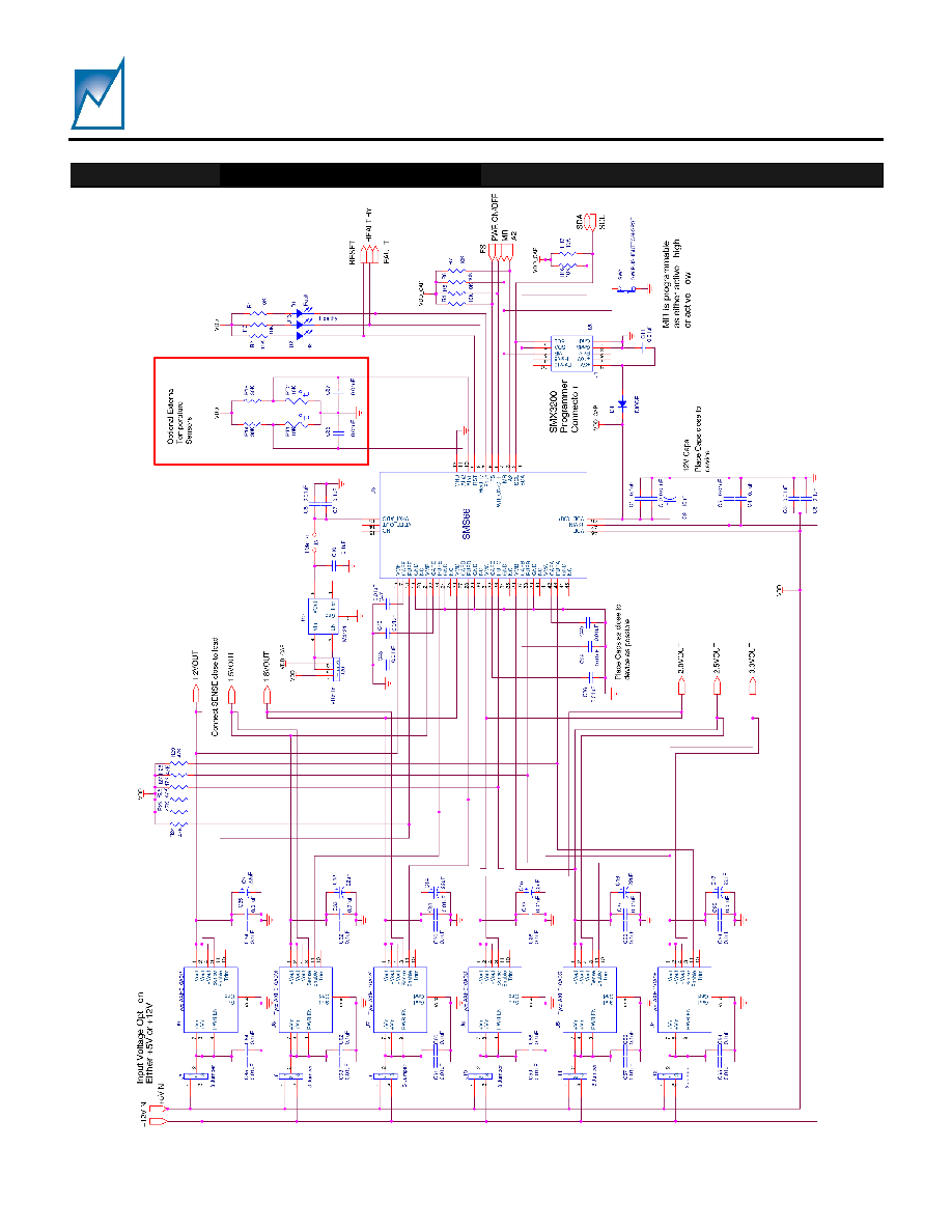
Figure 5 ≠ SMS66 Applications schematic.
APPLICATIONS INFORMATION (CONTINUED)
SMS66
Preliminary Information
Summit Microelectronics, Inc
2070 1.0 7/16/03
17
The end user can obtain the Summit SMX3200
programming system for device prototype
development. The SMX3200 system consists of a
programming Dongle, cable and Windows
TM
GUI
software. It can be ordered on the website or from a
local representative. The latest revisions of all
software and an application brief describing the
SMX3200 is available from the website
(
www.summitmicro.com
).
The SMX3200 programming Dongle/cable interfaces
directly between a PC's parallel port and the target
application. The device is then configured on-screen
via an intuitive graphical user interface employing
drop-down menus.
The Windows GUI software will generate the data and
send it in I
2
C serial bus format so that it can be directly
downloaded to the SMS66 via the programming
Dongle and cable. An example of the connection
interface is shown in Figure 6.
When design prototyping is complete, the software
can generate a HEX data file that should be
transmitted to Summit for approval. Summit will then
assign a unique customer ID to the HEX code and
program production devices before the final electrical
test operations. This will ensure proper device
operation in the end application.
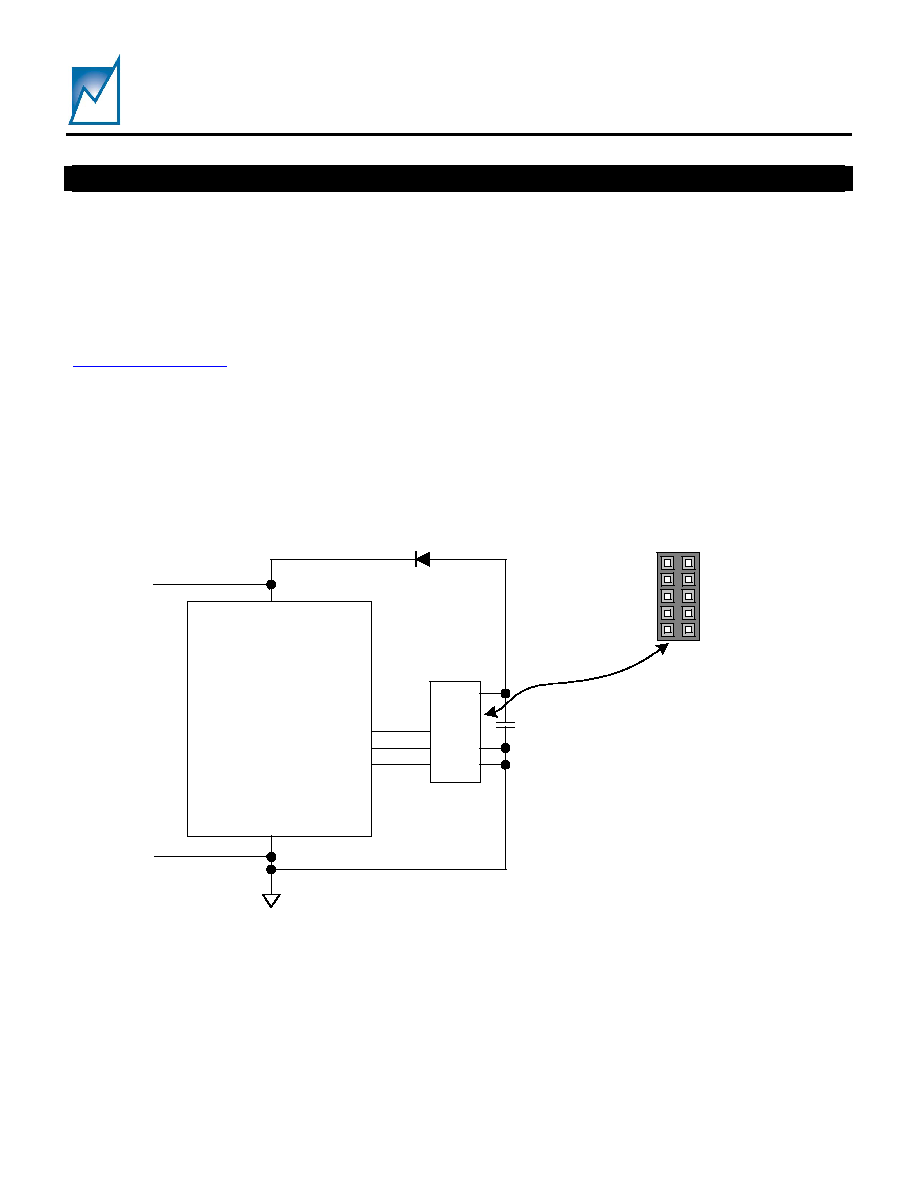
Pin 9, 5V
Pin 7, 10V
Pin 5, Reserved
Pin 3, GND
Pin 1, GND
Pin 6, MR#
Pin 4, SDA
Pin 2, SCL
Pin 8, Reserved
Pin 10, Reserved
Top view of straight 0.1" x 0.1 closed-side
connector. SMX3200 interface cable connector.
9
7
5
3
1
10
8
6
4
2
SMS66
SDA
SCL
VDD_CAP
GND
0.1
F
Positive
Supply
Common
Ground
MR
D1
1N4148
Figure 6≠ SMX3200 Programmer I
2
C serial bus connections to program the SMS66. Note that the MR pin
does not need to be connected to pin 6 for programming purposes.
DEVELOPMENT HARDWARE & SOFTWARE

SMS66
Preliminary Information
Summit Microelectronics, Inc
2070 1.0 7/16/03
18
SERIAL INTERFACE
Access to the configuration registers, general-purpose
memory and command and status registers is carried
out over an industry standard 2-wire serial interface
(I
2
C). SDA is a bi-directional data line and SCL is a
clock input. Data is clocked in on the rising edge of
SCL and clocked out on the falling edge of SCL. All
data transfers begin with the MSB. During data
transfers SDA must remain stable while SCL is high.
Data is transferred in 8-bit packets with an intervening
clock period in which an Acknowledge is provided by
the device receiving data. The SCL high period (t
HIGH
)
is used for generating Start and Stop conditions that
precede and end most transactions on the serial bus.
A high-to-low transition of SDA while SCL is high is
considered a Start condition while a low-to-high
transition of SDA while SCL is high is considered a
Stop condition.
The interface protocol allows operation of multiple
devices and types of devices on a single bus through
unique device addressing. The address byte is
comprised of a 4-bit device type identifier (slave
address) and a 3-bit bus address. The remaining bit
indicates either a read or a write operation. Refer to
Table 1 for a description of the address bytes used by
the SMS66.
The device type identifier for the memory array is
generally set to 1010
BIN
following the industry standard
for a typical nonvolatile memory. There is an option to
change the identifier to 1011
BIN
allowing it to be used
on a bus that may be occupied by other memory
devices. The configuration registers are grouped with
the memory array and thus use 1010
BIN
or 1011
BIN
as
the device type identifier. The command and status
registers as well as the 10-bit ADC are accessible with
the separate device type identifier of 1001
BIN
.
The bus address bits A1 and A0 are programmed into
the configuration registers. Bus address bit A[2] can
be programmed as either 0 or biased by the A2 pin.
The bus address accessed in the address byte of the
serial data stream must match the setting in the
SMS66 and on the A2 pin.
Any access to the SMS66 on the I2C bus will
temporarily halt the monitoring function. This is true
not only during the monitor mode, but also during
Power-on and Power-off sequencing when the device
is monitoring the channels to determine if they have
turned on or turned off.
The SMS66 halts the monitor function from when it
acknowledges the address byte until a valid stop is
received.
WRITE
Writing to the memory or a configuration register is
illustrated in Figures 8, 9, 11, 13 and 14. A Start
condition followed by the address byte is provided by
the host; the SMS66 responds with an Acknowledge;
the host then responds by sending the memory
address pointer or configuration register address
pointer; the SMS66 responds with an acknowledge;
the host then clocks in on byte of data. For memory
and configuration register writes, up to 15 additional
bytes of data can be clocked in by the host to write to
consecutive addresses within the same page. After
the last byte is clocked in and the host receives an
Acknowledge, a Stop condition must be issued to
initiate the nonvolatile write operation.
READ
The address pointer for the configuration registers,
memory, command and status registers and ADC
registers must be set before data can be read from the
SMS66. This is accomplished by a issuing a dummy
write command, which is simply a write command that
is not followed by a Stop condition. The dummy write
command sets the address from which data is read.
After the dummy write command is issued, a Start
command followed by the address byte is sent from
the host. The host then waits for an Acknowledge and
then begins clocking data out of the slave device. The
first byte read is data from the address pointer set
during the dummy write command. Additional bytes
can be clocked out of consecutive addresses with the
host providing an Acknowledge after each byte. After
the data is read from the desired registers, the read
operation is terminated by the host holding SDA high
during the Acknowledge clock cycle and then issuing a
Stop condition. Refer to Figures 10, 12 and 15 for an
illustration of the read sequence.
WRITE PROTECTION
The SMS66 powers up into a write protected mode.
Writing a code to the volatile write protection register
can disable the write protection. The write protection
register is located at address 87
HEX
of slave address
1001
BIN
.
Writing 0101
BIN
to bits [7:4] of the write protection
register allow writes to the general-purpose memory
while writing 0101
BIN
to bits [3:0] allow writes to the
configuration registers. The write protection can re-
I
2
C PROGRAMMING INFORMATION
SMS66
Preliminary Information
Summit Microelectronics, Inc
2070 1.0 7/16/03
19
enable by writing other codes (not 0101
BIN
) to the write
protection register. Writing to the write protection
register is shown in Figure 7.
CONFIGURATION REGISTERS
The majority of the configuration registers are grouped
with the general-purpose memory located at either
slave address 1010
BIN
or 1011
BIN
. The bus address
bits, A[1:0], used to differentiate the general-purpose
memory from the configuration registers are set to
11
BIN
. Bus address bit A[2] can be programmed as
either 0 or biased by the A2 pin.
Two additional configuration registers are located at
addresses 83
HEX
and 84
HEX
of slave address 1001
BIN
.
Writing and reading the configuration registers is
shown in Figures 8, 9, 10,11 and 12.
GENERAL-PURPOSE MEMORY
The 4k-bit general-purpose memory is located at
either slave address 1010
BIN
or 1011
BIN
. The bus
address bits, A[1:0], used to differentiate the general-
purpose memory from the configuration registers are
set to 00
BIN
for the first 2k-bits and 01
BIN
for the second
2k-bits. Bus address bit A[2] can be programmed as
either 0 or biased by the A2 pin. The word address
must be set each time the memory is accessed.
Memory writes and reads are shown in Figures 13, 14
and 15.
COMMAND AND STATUS REGISTERS
The command and status registers are located at
slave address 1001
BIN
. Writes and reads of the
command and status registers are shown in Figures
16 and 17.
ADC CONVERSIONS
An ADC conversion on any monitored channel can be
performed and read over the I
2
C bus using the ADC
read command. The ADC read command, shown in
Figure 18, starts with a dummy write to the 1001
BIN
slave address. Bits [6:3] of the word address byte are
used to address the desired monitored input. Once
the device acknowledges the channel address, it
begins the ADC conversion of the addressed input.
This conversion requires 70
µs to complete. During
this conversion time, acknowledge polling can be
used. The SMS66 will not acknowledge the address
bytes until the conversion is complete. When the
conversion has completed, the SMS66 will
acknowledge the address byte and return the 10-bit
conversion along with the 4-bit channel address echo.
GRAPHICAL USER INTERFACE (GUI)
Device configuration utilizing the Windows based
SMS66 graphical user interface (GUI) is highly
recommended. The software is available from the
Summit website (
www.summitmicro.com
). Using the
GUI in conjunction with this datasheet and Application
Note 33, simplifies the process of device prototyping
and the interaction of the various functional blocks. A
programming Dongle (SMX3200) is available from
Summit to communicate with the SMS66. The Dongle
connects directly to the parallel port of a PC and
programs the device through a cable using the I
2
C bus
protocol.
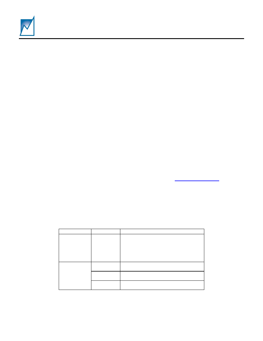
Slave Address Bus Address Register Type
1001
BIN
A2 A1 A0
Write Protection Register,
Command and Status Registers,
Two Configuration Registers,
ADC Conversion Readout
A2 0 0
1
st
2-k Bits of General-Purpose Memory
A2 0 1
2
nd
2-k Bits of General-Purpose Memory
1010
BIN
or
1011
BIN
A2 1 1
Configuration Registers
Table 1 - Address bytes used by the SMS66.
SMS66
Preliminary Information
Summit Microelectronics, Inc
2070 1.0 7/16/03
20
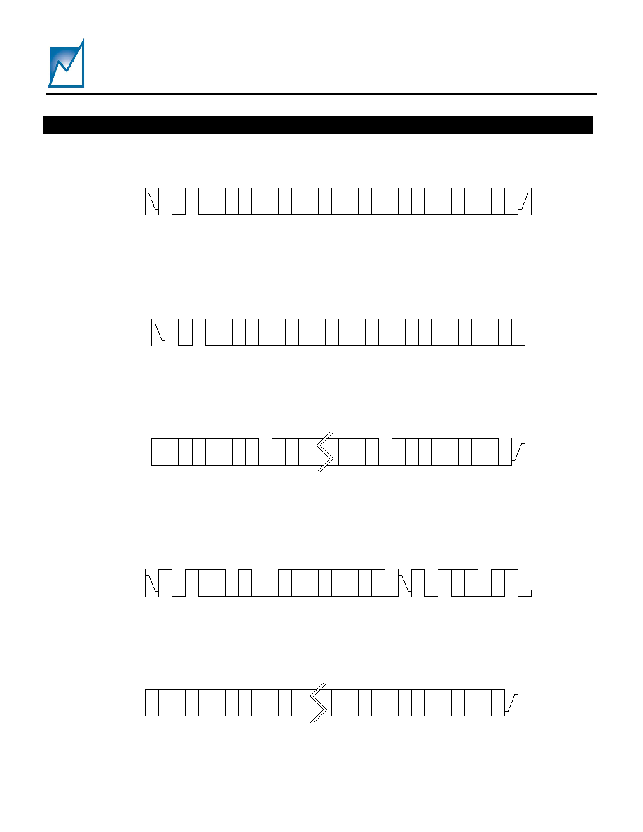
S
T
A
R
T
W
A
C
K
M aster
Slave
A
C
K
Configuration
Register Address = 87
HEX
1
0
0
0
0
1
1
1
0
1
0
1
0
1
0
1
S
T
O
P
Data = 55
HEX
A
C
K
1
0
0
1
A
2
Bus Address
A
1
A
0
5
HEX
Unlocks
General Purpose
EE
5
HEX
Unlocks
Configuration
Registers
W rite Protection
Register Address
8
HEX
7
HEX
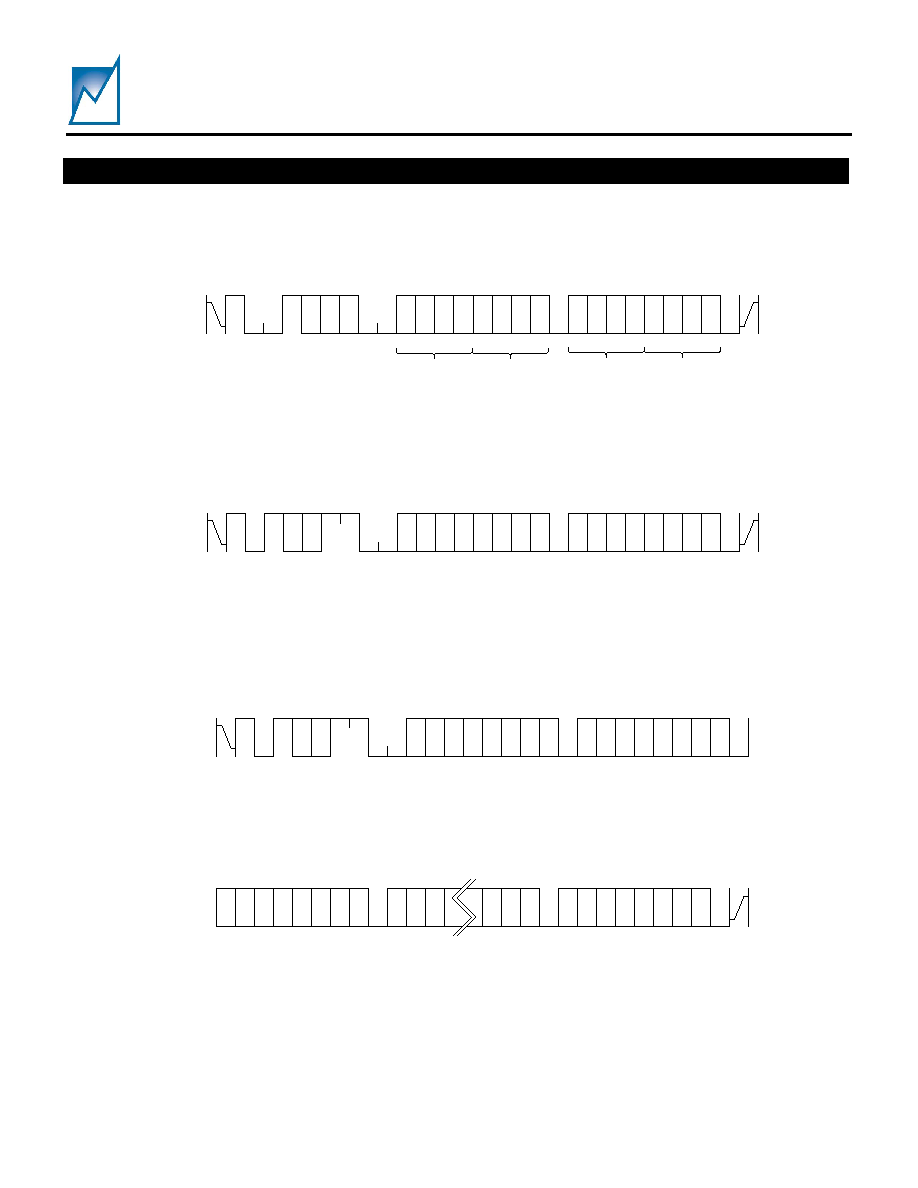
Figure 7 ≠ Write Protection Register Write
S
T
A
R
T
1
A
2
Bus Address
W
A
C
K
Master
Slave
A
C
K
1
1
0
1
S
A
0
Configuration
Register Address
C
7
C
6
C
5
C
4
C
3
C
2
C
1
C
0
D
7
D
6
D
5
D
4
D
3
D
2
D
1
D
0
S
T
O
P
Data
A
C
K
Figure 8 ≠ Configuration Register Byte Write
S
T
A
R
T
1
A
2
Bus Address
W
A
C
K
D
7
D
6
D
5
D
4
D
3
D
2
D
1
D
0
S
T
O
P
Master
Master
Slave
Slave
A
C
K
Data (16)
1
1
0
1
S
A
0
Configuration
Register Address
C
7
C
6
C
5
C
4
C
3
C
2
C
1
C
0
A
C
K
D
7
D
6
D
5
D
4
D
3
D
2
D
1
D
0
Data (1)
A
C
K
D
7
D
6
D
5
D
4
D
3
D
2
D
1
D
0
Data (2)
A
C
K
D
7
D
6
D
5
D
2
D
1
D
0
A
C
K
Figure 9 ≠ Configuration Register Page Write
I
2
C PROGRAMMING INFORMATION (CONTINUED)
SMS66
Preliminary Information
Summit Microelectronics, Inc
2070 1.0 7/16/03
21
S
T
A
R
T
1
A
2
Bus Address
W
A
C
K
D
7
D
6
D
5
D
4
D
3
D
2
D
1
D
0
S
T
O
P
N
A
C
K
Master
Master
Slave
Slave
A
C
K
Data (n)
1
1
0
1
S
A
0
Configuration
Register Address
C
7
C
6
C
5
C
4
C
3
C
2
C
1
C
0
S
T
A
R
T
1
R
A
C
K
A
2
Bus Address
1
1
S
A
0
0
1
A
C
K
D
7
D
6
D
5
D
2
D
1
D
0
A
C
K
D
7
D
6
D
5
D
4
D
3
D
2
D
1
D
0
Data (1)
Figure 10 - Configuration Register Read
S
T
A
R
T
W
A
C
K
Master
Slave
A
C
K
Configuration
Register Address
C
7
C
6
C
5
C
4
C
3
C
2
C
1
C
0
D
7
D
6
D
5
D
4
D
3
D
2
D
1
D
0
S
T
O
P
Data
A
C
K
1
0
0
1
A
2
Bus Address
A
1
A
0
Figure 11 - Configuration Register with Slave Address 1001
BIN
Write
S
T
A
R
T
W
A
C
K
D
7
D
6
D
5
D
4
D
3
D
2
D
1
D
0
S
T
O
P
N
A
C
K
Master
Master
Slave
Slave
A
C
K
Data (n)
Configuration
Register Address
C
7
C
6
C
5
C
4
C
3
C
2
C
1
C
0
S
T
A
R
T
R
A
C
K
A
C
K
D
7
D
6
D
5
D
2
D
1
D
0
A
C
K
D
7
D
6
D
5
D
4
D
3
D
2
D
1
D
0
Data (1)
1
0
0
1
A
2
Bus Address
A
1
A
0
1
0
0
1
A
2
Bus Address
A
1
A
0
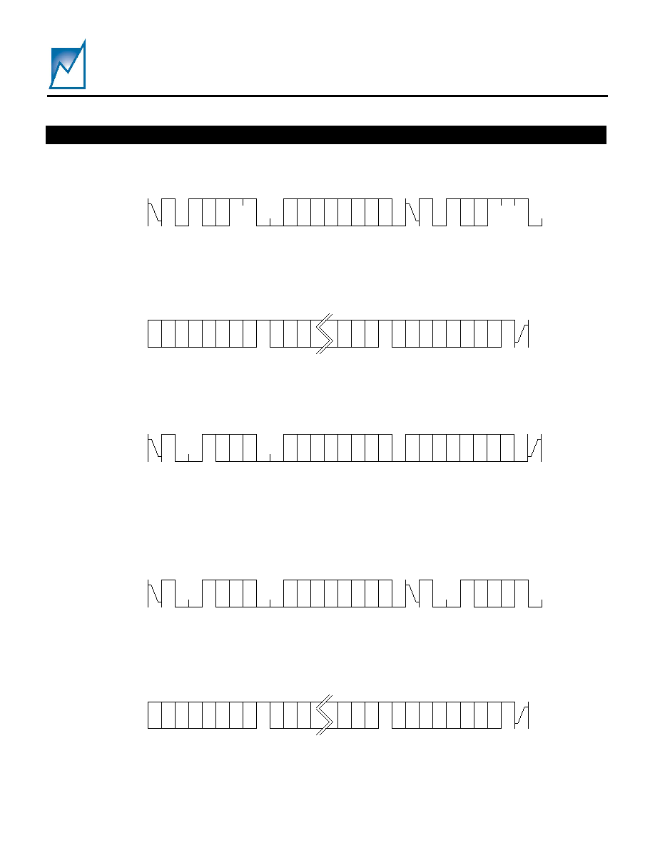
Figure 12 - Configuration Register with Slave Address 1001
BIN
Read
I
2
C PROGRAMMING INFORMATION (CONTINUED)
SMS66
Preliminary Information
Summit Microelectronics, Inc
2070 1.0 7/16/03
22
S
T
A
R
T
1
Bus Address
W
A
C
K
Master
Slave
A
C
K
0
1
S
A
0
Configuration
Register Address
C
7
C
6
C
5
C
4
C
3
C
2
C
1
C
0
D
7
D
6
D
5
D
4
D
3
D
2
D
1
D
0
S
T
O
P
Data
A
C
K
0
A
2
0
/
1
Figure 13 ≠ General Purpose Memory Byte Write
Bus Address
0
A
2
0
/
1
S
T
A
R
T
1
W
A
C
K
D
7
D
6
D
5
D
4
D
3
D
2
D
1
D
0
S
T
O
P
Master
Master
Slave
Slave
A
C
K
Data (16)
0
1
S
A
0
Configuration
Register Address
C
7
C
6
C
5
C
4
C
3
C
2
C
1
C
0
A
C
K
D
7
D
6
D
5
D
4
D
3
D
2
D
1
D
0
Data (1)
A
C
K
D
7
D
6
D
5
D
4
D
3
D
2
D
1
D
0
Data (2)
A
C
K
D
7
D
6
D
5
D
2
D
1
D
0
A
C
K
Figure 14 - General Purpose Memory Page Write
S
T
A
R
T
1
W
A
C
K
D
7
D
6
D
5
D
4
D
3
D
2
D
1
D
0
S
T
O
P
N
A
C
K
Master
Master
Slave
Slave
A
C
K
Data (n)
0
1
S
A
0
Configuration
Register Address
C
7
C
6
C
5
C
4
C
3
C
2
C
1
C
0
S
T
A
R
T
1
R
A
C
K
1
S
A
0
0
A
C
K
D
7
D
6
D
5
D
2
D
1
D
0
A
C
K
D
7
D
6
D
5
D
4
D
3
D
2
D
1
D
0
Data (1)
Bus Address
0
A
2
0
/
1
Bus Address
0
A
2
0
/
1
Figure 15 - General Purpose Memory Read
I
2
C PROGRAMMING INFORMATION (CONTINUED)
SMS66
Preliminary Information
Summit Microelectronics, Inc
2070 1.0 7/16/03
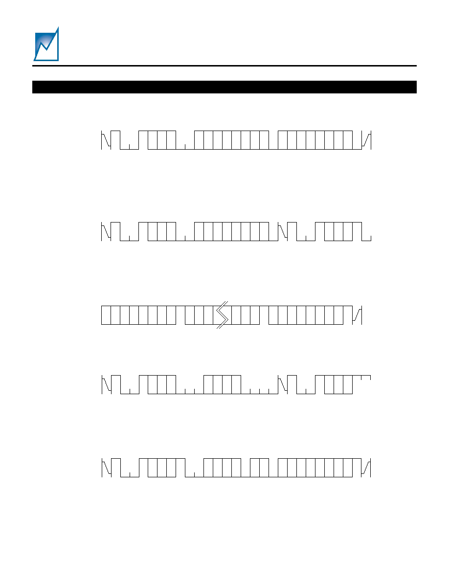
23
S
T
A
R
T
W
A
C
K
Master
Slave
A
C
K
Command and Status
Register Address
C
7
C
6
C
5
C
4
C
3
C
2
C
1
C
0
D
7
D
6
D
5
D
4
D
3
D
2
D
1
D
0
S
T
O
P
Data
A
C
K
1
0
0
1
A
2
Bus Address
A
1
A
0
Figure 16 ≠ Command and Status Register Write
S
T
A
R
T
W
A
C
K
D
7
D
6
D
5
D
4
D
3
D
2
D
1
D
0
S
T
O
P
N
A
C
K
Master
Master
Slave
Slave
A
C
K
Data (n)
Command and Status
Register Address
C
7
C
6
C
5
C
4
C
3
C
2
C
1
C
0
S
T
A
R
T
R
A
C
K
A
C
K
D
7
D
6
D
5
D
2
D
1
D
0
A
C
K
D
7
D
6
D
5
D
4
D
3
D
2
D
1
D
0
Data (1)
1
0
0
1
A
2
Bus Address
A
1
A
0
1
0
0
1
A
2
Bus Address
A
1
A
0
Figure 17 - Command and Status Register Read
S
T
A
R
T
1
0
0
1
A
2
Bus Address
A
1
A
0
W
C
H
3
C
H
2
C
H
1
C
H
0
A
C
K
S
T
A
R
T
1
0
0
1
A
2
Bus Address
A
1
A
0
R
S
T
A
R
T
1
0
0
1
A
2
Bus Address
A
1
A
0
R
C
H
3
C
H
2
C
H
1
C
H
0
D
9
D
8
D
7
D
6
D
5
D
4
D
3
D
2
D
1
D
0
S
T
O
P
N
A
C
K
N
A
C
K
Master
Master
Slave
Slave
Channel Address Echo
Channel Address
0
0
0
0
A
C
K
10-Bit ADC Data
A
C
K
A
C
K
0
0
Figure 18 ≠ ADC Conversion Read
I
2
C PROGRAMMING INFORMATION (CONTINUED)
SMS66
Preliminary Information
Summit Microelectronics, Inc
2070 1.0 7/16/03
24
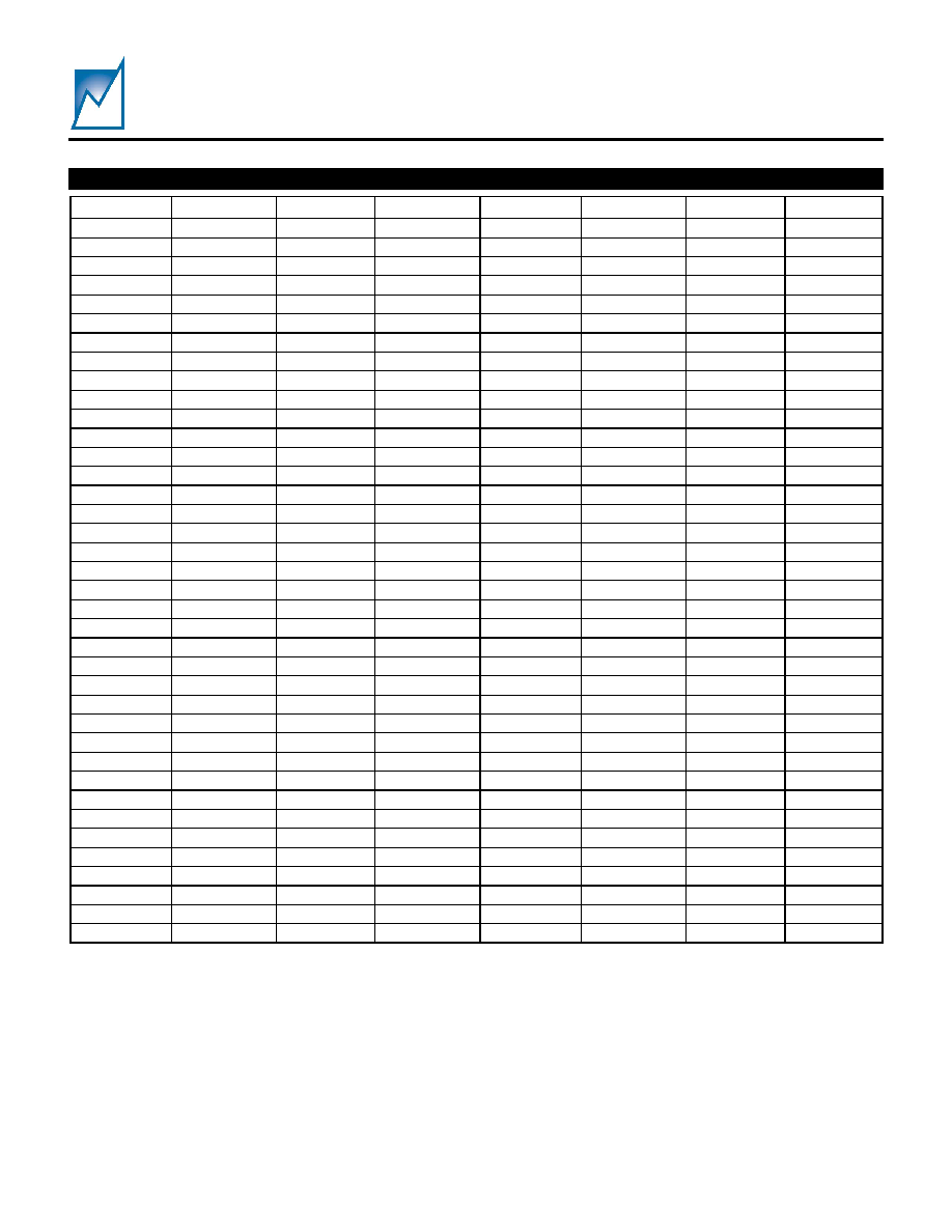
DEFAULT CONFIGURATION REGISTER SETTINGS ≠ SMS66-171
Register Contents Register Contents Register Contents Register Contents
R0C 00 R4B 7F
RA4
29
RCA 0C
R0D 00 R4C 00
RA5
5D
RCB 00
R0E 03 R80 42
RA6
11
RCC 0F
R0F
A1 R81 48
RA7
71
RCD FF
R10 8F R82 82
RA8
40
RCE 0F
R11 9F R83 3E
RA9
CE
RCF FF
R12
AF R84 2A
RAA
80
RD0 0C
R13 BF R85 B8
RAB
8F
RD1 00
R14 CF R86 12
RAC
29
RD2 0C
R15 DF R87 F6
RAD
1F
RD3 00
R18 00 R88 41
RAE
11
RD4 0F
R19 00 R89 C8
RAF
33
RD5 D8
R30 0D R8A 81
RB0
2A
RD6 0F
R31 60 R8B B9
RB1
67
RD7 D8
R32 0D R8C 2A
RB2
0A
RE0 00
R33 DC R8D 34
RB3
52
RE1 3D
R34 0E R8E 12
RB4
03
RE2 00
R35 45 R8F 49
RB5
FF
RE3 3D
R36 0E R90 49
RB6
03
RE4 00
R37
A2 R91 5C
RB7
FF
RE5 3D
R38 0F R92 81
RB8
0D
RE6 00
R39 08 R93 52
RB9
9A
RE7 3D
R3A 0F R94 29
RBA
0D
RE8 00
R3B D6 R95 D7
RBB
56
RE9 3D
R3C 00 R96 11
RBC
0F
REA 00
R3D 12 R97 EB
RBD
E0
REB 3D
R3E 48 R98 41
RBE
0F
R83 05
R40 0D R99 3E
RBF
E0
R84 00
R41 B9 R9A 81
RC0
0B
R42 0E R9B 33
RC1
38
R43 39 R9C 29
RC2
0B
R44 0E R9D 9A
RC3
38
R45
A4 R9E 11
RC4
09
R46 0F R9F AE
RC5
90
R47 16 RA0 41
RC6
09
R48 0F RA1 0B
RC7
90
R49 B4 RA2 80
RC8
0C
R4A 06 RA3 F6
RC9
00
RC1
The default device ordering number is SMS66F-171, is programmed as described above
and tested over the commercial temperature range. Application Note 42 contains a
complete description of the Windows GUI and the default settings of each of the 142
individual Configuration Registers.
SMS66
Preliminary Information
Summit Microelectronics, Inc
2070 1.0 7/16/03
25
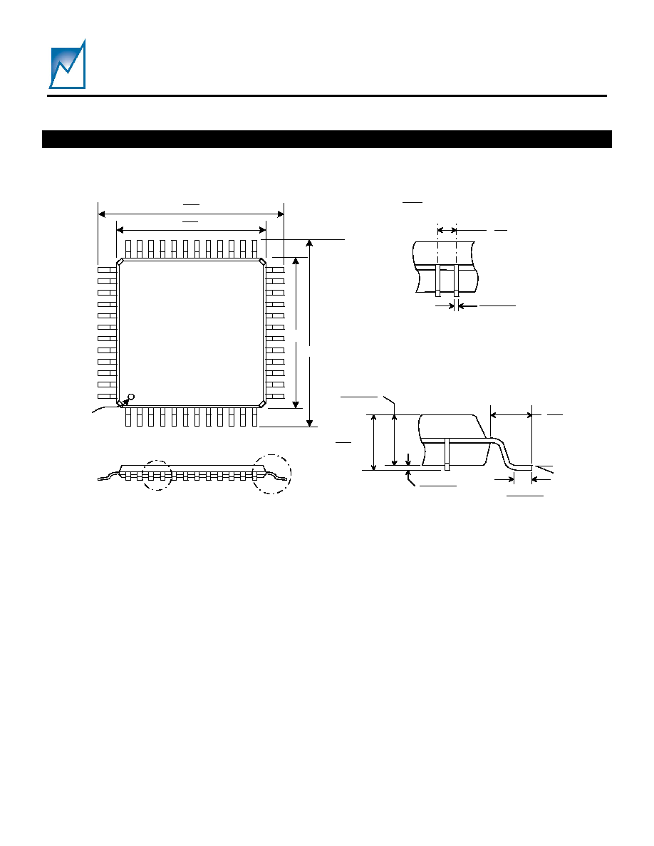
PACKAGE
A
B
Pin 1
Indicator
Inches
(Millimeters)
0.002 - 0.006
(0.05-0.15)
MAX.
0.047
(1.2)
0.037 - 0.041
0.95 - 1.05
0.018 - 0.030
(0.45 - 0.75)
0.039
(1.00)
0.02
(0.5)
BSC
0.007 - 0.011
(0.17 - 0.27)
DETAIL "A"
DETAIL "B"
(B)
(A)
(A)
0.354
(9.00) BSC
0.276
(7.00)
BSC (B)
48 PIN TQFP PACKAGE
0
o
Min to
7
o
Max
Ref Jedec M S-026
Ref
SMS66
Preliminary Information
Summit Microelectronics, Inc
2070 1.0 7/16/03
26
PART MARKING
SUMMIT
SMS66F
AYYW W
Pin 1
Annn
Summit Part Number
Date Code (YYW W )
Part Num ber suffix
(Contains Custom er specific ordering requirem ents)
Lot tracking code (Sum m it use)
Drawing not to scale
xx
Status Tracking Code
(Blank, MS, ES, 01, 02,...)
(Sum m it Use)
Product Tracking Code (Sum m it use)
ORDERING INFORMATION
NOTICE
NOTE 1 - This is a Preliminary Information data sheet that describes a Summit product currently in pre-production with limited characterization.
SUMMIT Microelectronics, Inc. reserves the right to make changes to the products contained in this publication in order to improve design,
performance or reliability. SUMMIT Microelectronics, Inc. assumes no responsibility for the use of any circuits described herein, conveys no license
under any patent or other right, and makes no representation that the circuits are free of patent infringement. Charts and schedules contained
herein reflect representative operating parameters, and may vary depending upon a user's specific application. While the information in this
publication has been carefully checked, SUMMIT Microelectronics, Inc. shall not be liable for any damages arising as a result of any error or
omission.
SUMMIT Microelectronics, Inc. does not recommend the use of any of its products in life support or aviation applications where the failure or
malfunction of the product can reasonably be expected to cause any failure of either system or to significantly affect their safety or effectiveness.
Products are not authorized for use in such applications unless SUMMIT Microelectronics, Inc. receives written assurances, to its satisfaction, that:
(a) the risk of injury or damage has been minimized; (b) the user assumes all such risks; and (c) potential liability of SUMMIT Microelectronics, Inc.
is adequately protected under the circumstances.
Revision 1.0 - This document supersedes all previous versions. Please check the Summit Microelectronics Inc. web site at
www.summitmicro.com
for data sheet updates.
© Copyright 2003 SUMMIT MICROELECTRONICS, Inc.
Power Management for CommunicationsTM
I2C is a trademark of Philips Corporation.
SMS66
F nnn
Package
F=48 Lead TQFP
Part Number Suffix (see page 24)
Summit Part Number
Specific requirements are contained in the suffix
such as Commercial or Industrial Temp Range,
Hex code, Hex code revision, etc.