 | –≠–ª–µ–∫—Ç—Ä–æ–Ω–Ω—ã–π –∫–æ–º–ø–æ–Ω–µ–Ω—Ç: SMS8198SA | –°–∫–∞—á–∞—Ç—å:  PDF PDF  ZIP ZIP |
SUMMIT MICROELECTRONICS, Inc. ∑ 300 Orchard City Drive, Suite 131 ∑ Campbell, CA 95008 ∑ Telephone 408-378-6461 ∑ Fax 408-378-6586 ∑ www.summitmicro.com
1
Characteristics subject to change without notice
© SUMMIT MICROELECTRONICS, Inc. 2000
2036 5.0 4/18/00
SUMMIT
MICROELECTRONICS, Inc.
SMS8198
FEATURES
∑
Designed to operate with the Philips
TriMedia Processor
∑
Coordinating the System Reset Function and
Providing the Processor's Configuration
Memory
∑
Multiple V
TRIP
Thresholds
-
No External Components Required
∑
Guaranteed Reset Assertion to V
CC
-1V
∑
Reset is an I/O
-
Allows System Reset Clean up
-
Provides a De-bounced Manual Reset Func-
tion
∑
Industry Standard 2-wire Serial Interface
∑
Hardware Write Lockout Function
∑
High Reliability
-
Endurance: 100,000 write cycles
-
Data Retention: 100 Years
Philips TriMediaTM Processor Companion Supervisor
With a 16K-bit 2-wire Serial Memory
OVERVIEW
The SMS8198 is a precision supervisory circuit designed
specifically as a companion chip for the Philips TriMedia
Processor family. The SMS8198 monitors the power
supply and holds the system in reset whenever V
CC
is
below the V
TRIP
threshold.
In addition to the supervisory function, the SMS8198 has
16K-bits of nonvolatile memory that is used by the
TriMedia processor as the boot memory.
The SMS8198 provides 16K-bits of memory that is acces-
sible through the industry standard 2-wire serial interface.
By integrating a precision supervisory circuit and the
hardware WP input, the SMS8198 becomes the perfect
companion chip for the Philips TriMedia processor family.
Its functions are integral to the boot hardware operation of
the TriMedia processors.
BLOCK DIAGRAM
+
≠
GND
VCC
8
4
TRI_RESET#
2
VTRIP
RESET
CONTROL
WP
7
1.26V
SCL
6
SDA
5
2036 T BD 2.0
WRITE
CONTROL
NONVOLATILE
MEMORY
ARRAY
PROGRAMMABLE
RESET PULSE
GENERATOR
2
SMS8198
2036 5.0 4/18/00
SMS8198
Tri Media
Processor
SDA
System Boot
Block
SCL
TRI_RESET#
VCR/Monitor
Audio
Local Reset
Audio
Camera
TRI_RESET#
PCI_RESET#
PCI Bus
WP
10K
4.7K
4.7K
4.7K
Peripheral
Peripheral
2036 ILL16.0
Figure 1. Typical Implementation of the SMS8198 and TriMedia Processor
The boot hardware operation begins with the assertion of
the reset signal TRI_RESET#. The TRI_RESET# output
from the SMS8198 is guaranteed to be valid at V
CC
-1.0V.
The reset output is asserted whenever V
CC
is less than the
V
TRIP
threshold and will remain asserted after V
CC
is
>V
TRIP
for the duration of t
PURST
. Whenever the
TRI_RESET# is active the memory will be write protected.
In addition to the reset write protection feature, pin 7 can
be tied to a pull-up to disable the write function of the
memory. This effectively turns the memory array into an
inexpensive boot ROM.
After reset is de-asserted, only the system boot block is
allowed to operate. At this point the TriMedia processor
takes over and begins to download data from the memory
array into its system boot block. The data downloaded
contains configuration data to set up the TriMedia proces-
sor and to load special ID information into the PCI configu-
ration space register. The ID information is published in
the PCI configuration register to provide the 16 bit Sub-
system ID and Subsystem Vendor ID.
It should be noted that both the threshold and the t
PURST
pulse width are programmable. Not only does this provide
maximum flexibility to the designer, but, as the processor
operating voltage levels migrate downwards, the
SMS8198 can be programmed to following this downward
trend. The values can be selected from the ordering
information table and the devices specified as standard
off-the-shelf items.
3
2036 5.0 4/18/00
SMS8198
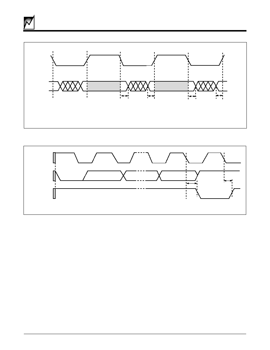
Figure 2. Reset Output Timing
Symbol
Parameter
Part no. Suffix
Min.
Typ.
Max.
Unit
VTRIP
Reset Trip Point
A (or) Blank
4.250
4.375
4.5
V
B
4.50
4.625
4.75
V
2.7
2.55
2.65
2.75
V
tPURST
Reset Timeout
200
ms
tRPD
VTRIP to RESET Output Delay
5
µs
VRVALID
RESET Output Valid to VCC min. Guarantee
1
V
tGLITCH
Glitch Reject Pulse Width note 1
30
ns
VOLRS
RESET Output Low Voltage IOL = 1mA
0.4
V
VOHRS
RESET High Voltage Output IOH = 800µA
RESET CIRCUIT AC and DC ELECTRICAL CHARACTERISTICS
T
A
= -40∞C to +85∞C
VCC
VRVALID
VTRIP
tPURST
2036 T fig02 2.0
tGLITCH
tRPD
tPURST
tRPD
TRI_RESET#
4
SMS8198
2036 5.0 4/18/00
TRI_RESET# - is an active low open drain output. It is
driven low whenever V
CC
is below V
TRIP
. TRI_RESET# is
also an input and can be used to debounce a switch input
or perform signal conditioning. The TRI_RESET# pin
does have an internal pull-up and should be left uncon-
nected if the signal is not used in the system. However,
when the pin is tied to a system TRI_RESET# line an
external pull-up resistor should be employed.
Write Protect (WP) - All write operations can be disabled
by maintaining WP > V
IH
.
No Connects (NC) - The no connect inputs are unused by
the SMS8198; however, to insure proper operation they
can be unconnected or tied to ground. They must not be
tied to V
CC
.
ENDURANCE AND DATA RETENTION
The SMS8198 is designed for applications requiring up to
100,000 erase/write cycles and unlimited read cycles. It
provides 100 years of secure data retention, with or
without power applied, after the execution of 100,000
erase/write cycles.
RESET CONTROLLER DESCRIPTION
The device provides a precise reset output to a
microcontroller and it's associated circuitry ensuring cor-
rect system operation during power-up/down conditions
and brownout situations. The output is open drain, allow-
ing control of the reset function by multiple devices.
During power-up the reset output remains in a fixed active
state until V
CC
passes through the reset threshold and
remains above the threshold for t
PURST
. The reset output
is valid whenever V
CC
is equal to or greater than 1V. If V
CC
falls below the threshold for more than t
GLITCH
the device
will immediately generate a reset and drive the output.
The reset pin is an I/O; therefore, forcing the pin to the
active state can also manually reset the device. Because
the I/O needs to be an open drain, the internal timer can
only be triggered by the leading edge of the input. The
resulting reset output will either be t
PURST
, or the externally
applied reset signal, whichever is longer. This can provide
an affective debounce or reset signal extender solution.
PIN DESCRIPTIONS
Serial Clock (SCL) - The SCL input is used to clock data
into and out of the device. In the WRITE mode, data must
remain stable while SCL is HIGH. In the READ mode, data
is clocked out on the falling edge of SCL.
Serial Data (SDA) - The SDA pin is a bidirectional pin
used to transfer data into and out of the device. Data may
change only when SCL is LOW, except START and STOP
conditions. It is an open-drain output and may be wire-
ORed with any number of open-drain or open-collector
outputs.
PIN NAMES
SDA
Serial Data I/O
SCL
Serial Clock Input
TRI_RESET#
Reset Output
GND
Ground
V
CC
Supply Voltage
WP
Write Protect
NC
No Connect
PIN CONFIGURATIONS
NC
TRI_RESET#
NC
GND
VCC
WP
SCL
SDA
1
2
3
4
8
7
6
5
8-Pin SOIC
2036 T PCon 2.0
5
2036 5.0 4/18/00
SMS8198
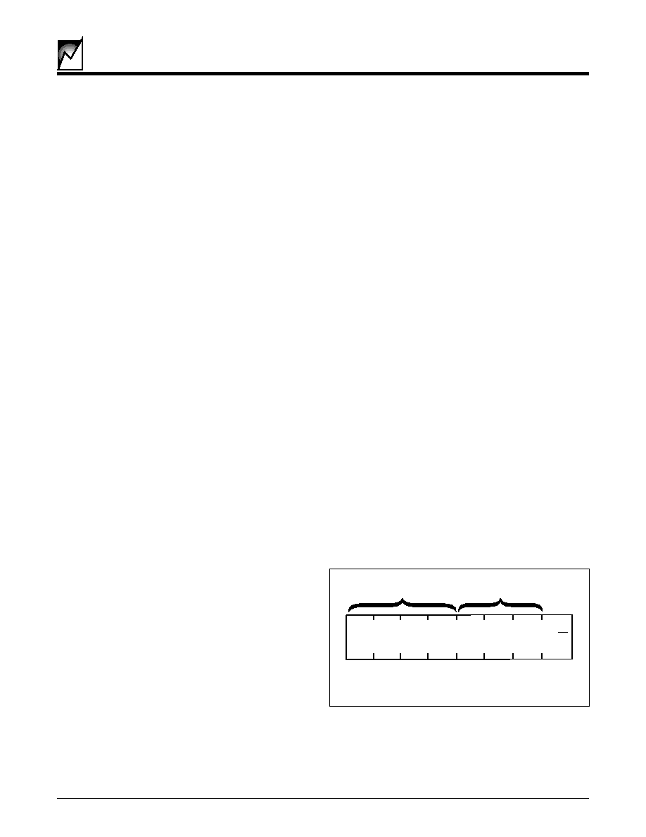
Figure 3. Input Data Protocol
Data must
remain stable
while clock
is HIGH.
Data must
remain stable
while clock
is HIGH.
Change
of data
allowed
SCL
SDA In
t
HD:DAT
t
SU:DAT
t
HD:DAT
2036 ILL4.0
Figure 4. Acknowledge Response From Receiver
SCL from
Master
Data Output
from
Transmitter
Data Output
from
Receiver
Start
Condition
ACKnowledge
t
AA
t
AA
1
8
9
2036 ILL6.0
6
SMS8198
2036 5.0 4/18/00
CHARACTERISTICS OF THE I
2
C BUS
General Description
The I
2
C bus was designed for two-way, two-line serial
communication between different integrated circuits. The
two lines are: a serial data line (SDA), and a serial clock
line (SCL). The SDA line must be connected to a positive
supply by a pull-up resistor, located somewhere on the
bus. Data transfer between devices may be initiated with
a START condition only when SCL and SDA are HIGH
(bus is not busy).
Input Data Protocol
One data bit is transferred during each clock pulse. The
data on the SDA line must remain stable during clock
HIGH time, because changes on the data line while SCL
is HIGH will be interpreted as start or stop condition (See
Figure 2).
START and STOP Conditions
When both the data and clock lines are HIGH, the bus is
said to be not busy. A HIGH-to-LOW transition on the data
line, while the clock is HIGH, is defined as the "START"
condition. A LOW-to-HIGH transition on the data line,
while the clock is HIGH, is defined as the "STOP" condi-
tion (See Figure 3).
DEVICE OPERATION
The SMS8198 is a 16,384-bit serial E
2
PROM. The device
supports the I
2
C bidirectional data transmission protocol.
The protocol defines any device that sends data onto the
bus as a "transmitter" and any device which receives data
as a "receiver." The device controlling data transmission
is called the "master" and the controlled device is called
the "slave." In all cases, the SMS8198 will be a "slave"
device, since it never initiates any data transfers.
Acknowledge (ACK)
Acknowledge is a software convention used to indicate
successful data transfers. The transmitting device, either
the master or the slave, will release the bus after transmit-
Figure 5. Slave Address Byte
ting eight bits. During the ninth clock cycle, the receiver will
pull the SDA line LOW to ACKnowledge that it received the
eight bits of data (See Figure 4).
The SMS8198 will respond with an ACKnowledge after
recognition of a START condition and its slave address
byte. If both the device and a write operation are selected,
the SMS8198 will respond with an ACKnowledge after the
receipt of each subsequent 8-bit word.
In the READ mode, the SMS8198 transmits eight bits of
data, then releases the SDA line, and monitors the line for
an ACKnowledge signal. If an ACKnowledge is detected,
and no STOP condition is generated by the master, the
SMS8198 will continue to transmit data. If an
ACKnowledge is not detected, the SMS8198 will terminate
further data transmissions and awaits a STOP condition
before returning to the standby power mode.
Device Addressing
Following a start condition the master must output the
address of the slave it is accessing. The most significant
four bits of the slave address are the device type identifier
(see figure 5). For the SMS8198 this is fixed as 1010
bin
.
Word Address
The next three bits of the slave address are an extension
of the array's address and are concatenated with the eight
bits of address in the word address field, providing direct
access to the 2,048 X 8 array.
Read/Write Bit
The last bit of the data stream defines the operation to be
performed. When set to "1," a read operation is selected;
when set to "0," a write operation is selected.
1 0 1 0
A10 A9 A8 R/W
DEVICE
IDENTIFIER
HIGH ORDER
WORD ADDRESS
2036 ILL7.0
7
2036 5.0 4/18/00
SMS8198
Figure 6. Page/Byte WRITE Mode
WRITE OPERATIONS
The SMS8198 allows two types of write operations: byte
write and page write. The byte write operation writes a
single byte during the nonvolatile write period (t
WR
). The
page write operation allows up to 16 bytes in the same
page to be written during t
WR
.
Byte WRITE
After the slave address is sent (to identify the slave
device, specify high order word address and a read or
write operation), a second byte is transmitted which
contains the low 8 bit addresses of any one of the 2,048
words in the array.
Upon receipt of the word address, the SMS8198 re-
sponds with an ACKnowledge. After receiving the next
byte of data, it again responds with an ACKnowledge. The
master then terminates the transfer by generating a
STOP condition, at which time the SMS8198 begins the
internal write cycle.
While the internal write cycle is in progress, the SMS8198
inputs are disabled, and the device will not respond to any
requests from the master. Refer to Figure 6 for the
address, ACKnowledge and data transfer sequence.
Page WRITE
The SMS8198 is capable of a 16-byte page write opera-
tion. It is initiated in the same manner as the byte-write
operation, but instead of terminating the write cycle after
the first data word, the master can transmit up to 15 more
words of data. After the receipt of each word, the
SMS8198 will respond with an ACKnowledge.
The SMS8198 automatically increments the address for
subsequent data words. After the receipt of each word,
the four low order address bits are internally incremented
by one. The high order five bits of the address byte remain
constant. Should the master transmit more than sixteen
words, prior to generating the STOP condition, the ad-
dress counter will "roll over," and the previously written
data will be overwritten. As with the byte-write operation,
all inputs are disabled during the internal write cycle.
Refer to Figure 6 for the address, ACKnowledge and data
transfer sequence.
D
7
D
6
D
5
D
4
D
3
D
2
D
1
D
0
D
7
D
6
D
5
D
4
D
3
D
2
D
1
D
0
A
7
A
6
A
5
A
4
A
3
A
2
A
1
A
0
D
7
D
5
D
6
D
4
D
0
D
3
D
2
D
1
S
T
A
R
T
Word Address
Data Byte n
Data Byte n+15
S
T
O
P
A
C
K
Acknowledges Transmitted from
SMS8198 to Master Receiver
Slave Address
Device
Type
Address
Read/Write
0= Write
A10,A9,A8
SDA
Bus
Activity
A
C
K
A
C
K
Master Sends Read
Request to Slave
Master Writes Word
Address to Slave
1 0 1 0
0
Data Byte n+1
A
C
K
Master Writes
Data to Slave
Master Transmitter
to
Slave Receiver
Slave Transmitter
to
Master Receiver
Slave Transmitter
to
Master Receiver
Master Transmitter
to
Slave Receiver
Master Transmitter
to
Slave Receiver
Shading Denotes
SMS8198
SDA Output Active
Master Transmitter
to
Slave Receiver
Slave Transmitter
to
Master Receiver
Slave Transmitter
to
Master Receiver
Master Transmitter
to
Slave Receiver
Slave Transmitter
to
Master Receiver
Master Writes
Data to Slave
Master Writes
Data to Slave
Acknowledges Transmitted from
SMS8198 to Master Receiver
If single byte-write only,
Stop bit issued here.
A
10
A
9
R
W
A
C
K
A
8
2036 ILL8.0
8
SMS8198
2036 5.0 4/18/00
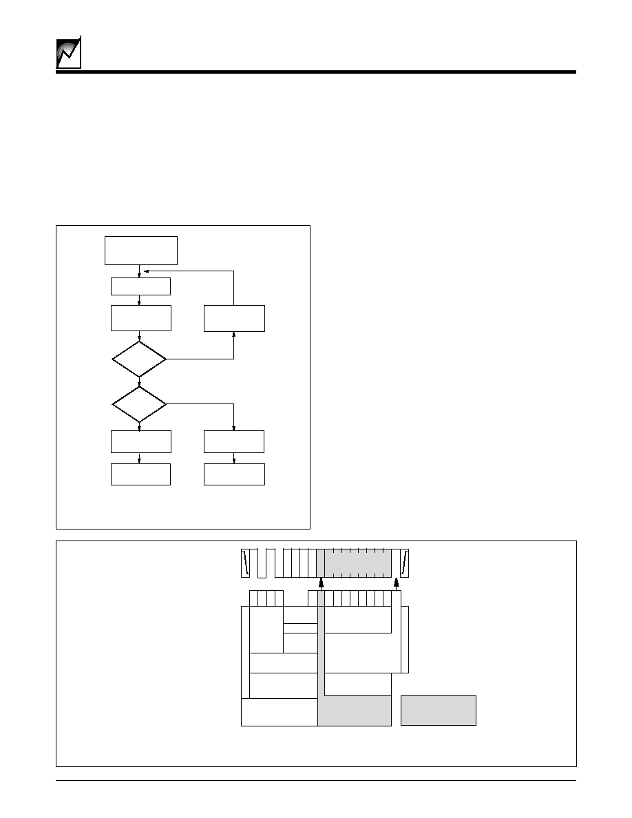
Figure 8. Current Address Byte Read Mode
Figure 7. Acknowledge Polling
Acknowledge Polling
When the SMS8198 is performing an internal WRITE
operation, it will ignore any new START conditions. Since
the device will only return an acknowledge after it accepts
the START, the part can be continuously queried until an
acknowledge is issued, indicating that the internal WRITE
cycle is complete.
To poll the device, give it a START condition, followed by
a slave address for a WRITE operation (See Figure 7).
READ OPERATIONS
Read operations are initiated with the R/W bit of the
identification field set to "1." There are four different read
options:
1.
Current Address Byte Read
2.
Random Address Byte Read
3.
Current Address Sequential Read
4.
Random Address Sequential Read
Current Address Byte Read
The SMS8198 contains an internal address counter
which maintains the address of the last word accessed,
incremented by one. If the last address accessed (either
a read or write) was to address location n, the next read
operation would access data from address location n+1
and increment the current address pointer. When the
SMS8198 receives the slave address field with the R/W
bit set to "1," it issues an acknowledge and transmits the
8-bit word stored at address location n+1.
The current address byte read operation only accesses a
single byte of data. The master does not acknowledge the
transfer, but does generate a stop condition. At this point,
the SMS8198 discontinues data transmission. See Fig-
ure 8 for the address acknowledge and data transfer
sequence.
Issue Start
Internal WRITE Cycle
In Progress;
Begin ACK Polling
Issue Slave
Address and
R/W = 0
ACK
Returned?
Next
operation a
WRITE?
Issue Byte
Address
Proceed with
WRITE
Issue Stop
Await Next
Command
Issue Stop
No
No
Yes (Internal WRITE Cycle is completed)
Yes
2036 ILL9.0
S
T
A
R
T
S
T
O
P
Slave Address
Device
Type
Address
Read/Write
1= Read
A10,A9,A8
SDA Bus Activity
D
7
D
6
D
5
D
4
D
3
D
2
D
1
D
0
Master sends Read
request to Slave
Slave sends
Data to Master
Master Transmitter
to
Slave Receiver
Slave Transmitter
to
Master Receiver
1
1
1
0
0
1
Lack of ACK (low)
from Master
determines last
data byte to be read
1
Shading Denotes
SMS8198
SDA Output Active
A
9
A
10
R
W
A
C
K
A
8
Data Byte
2036 ILL10.0
9
2036 5.0 4/18/00
SMS8198
Figure 9. Random Address Byte Read Mode
Random Address Byte Read
Random address read operations allow the master to
access any memory location in a random fashion. This
operation involves a two-step process. First, the master
issues a write command which includes the start condi-
tion and the slave address field (with the R/W bit set to
WRITE) followed by the address of the word it is to read.
This procedure sets the internal address counter of the
SMS8198 to the desired address.
After the word address acknowledge is received by the
master, the master immediately reissues a start condition
followed by another slave address field with the R/W bit
set to READ. The SMS8198 will respond with an acknowl-
edge and then transmit the 8-data bits stored at the
addressed location. At this point, the master does not
acknowledge the transmission but does generate the stop
condition. The SMS8198 discontinues data transmission
and reverts to its standby power mode. See Figure 9 for
the address, acknowledge and data transfer sequence.
D
7
D
6
D
5
D
4
D
3
D
2
D
1
D
0
A
7
A
6
A
5
A
4
A
3
A
2
A
1
A
0
S
T
A
R
T
Word Address
S
T
O
P
A
C
K
Slave Address
Slave Address
Device
Type
Address
Read/Write
0= Write
Device
Type
Address
A10,A9,A8
A10,A9,A8
SDA Bus
Activity
S
T
A
R
T
Read/Write
1= Read
A
C
K
A
C
K
Master sends Read
request to Slave
Master Writes Word
Address to Slave
Master Requests
Data from Slave
Slave sends
Data to Master
1 0 1 0
1 0 1 0
1
0
A
10
A
9
R
W
A
8
A
9
R
W
A
10
A
8
Lack of ACK (low)
from Master
determines last
data byte to be read
1
Slave Transmitter
to
Master Receiver
Slave Transmitter
to
Master Receiver
Shading Denotes
SMS8198
SDA Output Active
Slave Transmitter
to
Master Receiver
Master Transmitter
to
Slave Receiver
Master Transmitter
to
Slave Receiver
Master Transmitter
to
Slave Receiver
Slave Transmitter
to
Master Receiver
Data Byte
2036 ILL11.0
10
SMS8198
2036 5.0 4/18/00
Sequential READ
Sequential READs can be initiated as either a current
address READ or random access READ. The first word is
transmitted as with the other byte read modes (current
address byte READ or random address byte READ);
however, the master now responds with an ACKnowledge,
indicating that it requires additional data from the
SMS8198. The SMS8198 continues to output data for
each ACKnowledge received. The master terminates the
sequential READ operation by not responding with an
ACKnowledge, and issues a STOP conditions.
During a sequential read operation, the internal address
counter is automatically incremented with each acknowl-
edge signal. For read operations, all address bits are
incremented, allowing the entire array to be read using a
single read command. After a count of the last memory
address, the address counter will `roll-over' and the
memory will continue to output data. See Figure 10 for the
address, acknowledge and data transfer sequence.
Figure 10. Sequential READ Operation (starting with a Random Address READ)
D
7
D
6
D
5
D
4
D
3
D
2
D
1
D
0
D
7
D
6
D
5
D
4
D
3
D
2
D
1
D
0
A
7
A
6
A
5
A
4
A
3
A
2
A
1
A
0
Shading Denotes
SMS8198
SDA Output Active
S
T
A
R
T
Word Address
S
T
O
P
A
C
K
Acknowledges from SMS8198
Slave Address
Slave Address
Device
Type
Address
Read/Write
0= Write
Device
Type
Address
A10,A9,A8
A10,A9,A80
SDA Bus
Activity
S
T
A
R
T
Read/Write
1= Read
A
9
R
W
A
10
Acknowledge from
Master Receiver
A
C
K
A
C
K
A
C
K
Master sends Read
request to Slave
Master Writes Word
Address to Slave
Master Requests
Data from Slave
Slave sends
Data to Master
Slave Transmitter
to
Master Receiver
Slave Transmitter
to
Master Receiver
Master Transmitter
to
Slave Receiver
1 0 1 0
1 0 1 0
1
0
Slave sends
Data to Master
A
10
A
9
R
W
A
8
A
8
Lack of ACK (low)
determines last
data byte to be read
1
Lack of
Acknowledge from
Master Receiver
Slave Transmitter
to
Master Receiver
Master Transmitter
to
Slave Receiver
Master Transmitter
to
Slave Receiver
Master Transmitter
to
Slave Receiver
Slave Transmitter
to
Master Receiver
Slave Transmitter
to
Master Receiver
Last Data Byte
First Data Byte
2036 ILL12.0
11
2036 5.0 4/18/00
SMS8198
ABSOLUTE MAXIMUM RATINGS
Temperature Under Bias
............................................................................................................... -40∞C to +85∞C
Storage Temperature ..................................................................................................................... -65∞C to +125∞C
Soldering Temperature (less than 10 seconds) .............................................................................................. 300∞C
Supply Voltage ........................................................................................................................................... 0 to 6.5V
Voltage on Any Pin ...................................................................................................................... -0.3V to V
CC
+0.3V
ESD Voltage (JEDEC method) ...................................................................................................................... 2,000V
NOTE: These are STRESS ratings only. Appropriate conditions for operating these devices are given elsewhere in this specification. Stresses
beyond those listed here may permanently damage the part. Prolonged exposure to maximum ratings may affect device reliability.
DC ELECTRICAL CHARACTERISTICS
SMS8198, T
A
= -40∞C to +85∞C, V
CC
= 2.7V to 5.5V
Symbol
Parameter
Conditions
Min
Max
Units
SCL = CMOS Levels @ 100KHz
V
CC
=5.5V
3
mA
I
CC
Supply Current (CMOS)
SDA = Open
All other inputs = GND or V
CC
V
CC
=3.3V
2
mA
I
SB
Standby Current (CMOS)
SCL = SDA = V
CC
V
CC
=5.5V
50
µA
All other inputs = GND
I
LI
Input Leakage
V
IN
= 0 To V
CC
10
µA
I
LO
Output Leakage
V
OUT
= 0 To V
CC
10
µA
V
IL
Input Low Voltage
S0, S1, S2, SCL, SDA, RESET
0.3xV
CC
V
V
IH
Input High Voltage
S0, S1, S2, SCL, SDA
0.7xV
CC
V
V
OL
Output Low Voltage
I
OL
= 3mA
0.4
V
V
ROL
RESET
Low Output
V
CC
= 1.0V, I
OL
= 100µA
0.3
V
V
CC
= 2.7V, I
OL
= 400µA
0.3
V
V
CC
= 4.5V, I
OL
= 1mA
0.4
V
V
CC
=3.3V
25
µA
2036 PGM T1.1
l
o
b
m
y
S
r
e
t
e
m
a
r
a
P
s
n
o
i
t
i
d
n
o
C
V
5
.
4
o
t
V
7
.
2
V
5
.
5
o
t
V
5
.
4
s
t
i
n
U
.
n
i
M
.
x
a
M
.
n
i
M
.
x
a
M
f
L
C
S
y
c
n
e
u
q
e
r
f
k
c
o
l
c
L
C
S
0
0
0
1
0
0
4
z
H
k
t
W
O
L
d
o
i
r
e
p
w
o
l
k
c
o
l
C
7
.
4
3
.
1
s
µ
t
H
G
I
H
d
o
i
r
e
p
h
g
i
h
k
c
o
l
C
0
.
4
6
.
0
s
µ
t
F
U
B
e
m
i
t
e
e
r
f
s
u
B
n
o
i
s
s
i
m
s
n
a
r
t
w
e
n
e
r
o
f
e
B
7
.
4
3
.
1
s
µ
t
A
T
S
:
U
S
e
m
i
t
p
u
t
e
s
n
o
i
t
i
d
n
o
c
t
r
a
t
S
7
.
4
6
.
0
s
µ
t
A
T
S
:
D
H
e
m
i
t
d
l
o
h
n
o
i
t
i
d
n
o
c
t
r
a
t
S
0
.
4
6
.
0
s
µ
t
O
T
S
:
U
S
e
m
i
t
p
u
t
e
s
n
o
i
t
i
d
n
o
c
p
o
t
S
7
.
4
6
.
0
s
µ
t
A
A
t
u
p
t
u
o
o
t
k
c
o
l
C
d
il
a
v
t
u
O
a
t
a
D
A
D
S
o
t
w
o
l
L
C
S
3
.
0
5
.
3
2
.
0
9
.
0
s
µ
t
H
D
e
m
i
t
d
l
o
h
t
u
O
a
t
a
D
e
g
n
a
h
c
t
u
O
a
t
a
D
A
D
S
o
t
w
o
l
L
C
S
3
.
0
2
.
0
s
µ
t
R
e
m
i
t
e
s
i
r
A
D
S
d
n
a
L
C
S
1
3
.
0
s
µ
t
F
e
m
i
t
ll
a
f
A
D
S
d
n
a
L
C
S
3
.
0
3
.
0
s
µ
t
T
A
D
:
U
S
e
m
i
t
p
u
t
e
s
n
I
a
t
a
D
0
5
2
0
0
1
s
n
t
T
A
D
:
D
H
e
m
i
t
d
l
o
h
n
I
a
t
a
D
0
0
s
n
t
I
L
C
S
@
h
t
d
i
w
e
k
i
p
s
e
s
i
o
N
s
t
u
p
n
i
A
D
S
&
t
n
a
t
s
n
o
c
e
m
i
t
n
o
i
s
e
r
p
p
u
s
e
s
i
o
N
0
0
1
0
0
1
s
n
t
R
W
e
m
i
t
e
l
c
y
c
e
t
i
r
W
0
1
0
1
s
m
AC ELECTRICAL CHARACTERISTICS
SMS8198, T
A
= -40∞C to +85∞C, V
CC
= 2.7V to 5.5V
12
SMS8198
2036 5.0 4/18/00
Figure 11. Bus Timing
CAPACITANCE
T
A
= 25∞C, f = 100KHz
Symbol
Parameter
Max
Units
C
IN
Input Capacitance
5
pF
C
OUT
Output Capacitance
8
pF
2036 PGM T3.0
tF
tR
tLOW
tHIGH
tHD:SDA
tSU:SDA
tBUF
tDH
tHD:DAT
tSU:DAT
tSU:STO
SCL
SDA In
SDA Out
tAA
2047 Fig07 1.0

13
2036 5.0 4/18/00
SMS8198
ORDERING INFORMATION
V
TRIP
Threshold
A or Blank = 4.5V
B = 4.75V
2.7 = 2.7V
SMS8198
S
A
Base Part Number
Package
S = 8 Lead SOIC
2036 Tree 2.0
14
SMS8198
2036 5.0 4/18/00
NOTICE
SUMMIT Microelectronics, Inc. reserves the right to make changes to the products contained in this publication in order to improve
design, performance or reliability. SUMMIT Microelectronics, Inc. assumes no responsibility for the use of any circuits described
herein, conveys no license under any patent or other right, and makes no representation that the circuits are free of patent
infringement. Charts and schedules contained herein reflect representative operating parameters, and may vary depending upon
a user's specific application. While the information in this publication has been carefully checked, SUMMIT Microelectronics, Inc.
shall not be liable for any damages arising as a result of any error or omission.
SUMMIT Microelectronics, Inc. does not recommend the use of any of its products in life support applications where the failure
or malfunction of the product can reasonably be expected to cause failure of the life support system or to significantly affect its
safety or effectiveness. Products are not authorized for use in such applications unless SUMMIT Microelectronics, Inc. receives
written assurances, to its satisfaction, that: (a) the risk of injury or damage has been minimized; (b) the user assumes all such risks;
and (c) potential liability of SUMMIT Microelectronics, Inc. is adequately protected under the circumstances.
I
2
C is a trademark of Philips Corporation.
© Copyright 2000 SUMMIT Microelectronics, Inc.
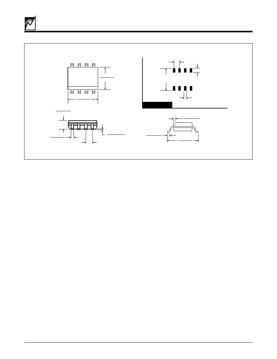
.228 (5.80)
.244 (6.20)
.016 (.40)
.035 (.90)
.020 (.50)
.010 (.25)
x45
∞
.0192 (.49)
.0138 (.35)
.061 (1.75)
.053 (1.35)
.0098 (.25)
.004 (.127)
.05 (1.27) TYP.
.275 (6.99) TYP.
.030 (.762) TYP.
8 Places
.050 (1.27) TYP.
.050 (1.270) TYP.
8 Places
.157 (4.00)
.150 (3.80)
.196 (5.00)
1
.189 (4.80)
FOOTPRINT
8pn JEDEC SOIC ILL.2
8 Pin SOIC (Type S) Package JEDEC (150 mil body width)