 | –≠–ª–µ–∫—Ç—Ä–æ–Ω–Ω—ã–π –∫–æ–º–ø–æ–Ω–µ–Ω—Ç: SMT2002GC | –°–∫–∞—á–∞—Ç—å:  PDF PDF  ZIP ZIP |

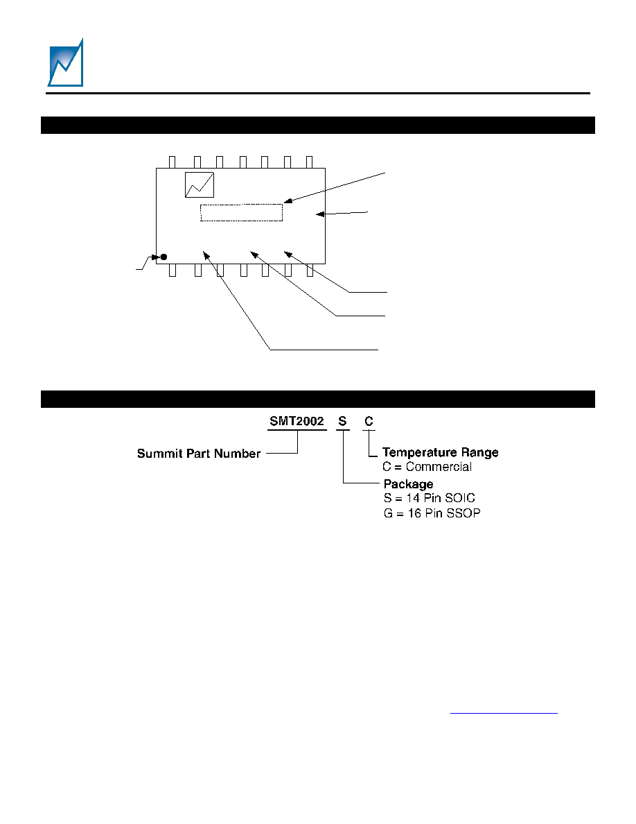
SMT2002
Preliminary Information
1
(See Last Page)
© SUMMIT Microelectronics, Inc. 2001 ∑
300 Orchard City Drive, #131 ∑ Campbell CA 95006
∑ Phone 408 378-6461 ∑ FAX 408 378-6596 www.summitmicro.com
2063 4.2 1/23/03
1
FEATURES & APPLICATIONS
∑ Controls Track Up/Down 2 Supply Voltages
∑ Standalone or Works with SMS24, SMS44, or
SMS64 Sequencing Controllers
∑ Limits Supply Differential to <100mV
- Both Power-on and Power-off
∑ On-Board Charge Pump to Fully Enhance Low
R
DS(ON)
MOSFETs
∑ Packaged in 14 Lead SOIC and 16 Lead SSOP
Applications
∑ Multi-Voltage Supply Rail Manager
∑ CPE Equipment
∑ Telecom/Datacom Motherboards/Servers
∑ Mezzanine Line Cards
- Compact PCI
TM
Hot Swap Control
- Network Processors, DSPs, ASICs
∑ Multi-voltage Network Processors, DSPs,
ASICs
INTRODUCTION
The SMT2002 is a low cost two-channel tracking
controller that can be used alone or in tandem with a
SMS24, SMS44 or SMS64 sequencing controller
where differential voltage tracking of two supplies is
needed. It can also be used as a standalone function
with any power supply system. It will track two input
channels to an internal ramp set to 500V/S.
The SMT2002 does not monitor the input
channels before it begins tracking. However, the VIN
inputs must be at their nominal voltages before the
PWR_ON# pin is asserted. The SMT2002 matches
well with a sequencer that can provide an active low
signal to indicate that the SMT2002 can begin
tracking. The sequencer can also be used to monitor
the voltage channels. The SMT2002 includes a status
output that indicates when track up and when track
down are complete.
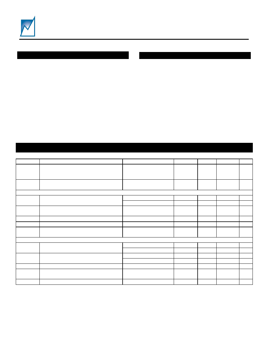
SIMPLIFIED APPLICATIONS DRAWING
VD D
VG G _CAP
PW R_O N #
G ND
VG ATE V
STATUS #
SM T2002
VI
NA
VG
A
T
E
A
VO UTA
VI
NB
VG
A
T
E
B
VO UTB
1µF
1.5VIN
2.5VIN
2.5VO UT
1.5VO UT
G ND
G ND
EN AB LE#
STATUS #
10nF
10
3.3 VD D
VD D
10nF
10
0.1µF
FS #
Forced
Shutdow n#
VD D
VD D
Figure 1 ≠ Typical Applications Schematic using the SMT2002 TRAKKER
TM
Controller
Dual Channel TRAKKER
TM
Controller
SMT2002
Preliminary Information
Summit Microelectronics, Inc
2063 4.2 1/23/03
2
GENERAL DESCRIPTION
The SMT2002 is a fully integrated power supply
tracking controller designed for use in Point-of-Load
(POL) power applications or in multi-supply rail circuit
cards. The supplies can be resident on the circuit card
in the form of LDO's or DC-to-DC converters, or the
supplied voltages can be present on the backplane of
the system.
A key function of the SMT2002 is the external
power MOSFET control. The device can be used to
turn on MOSFETs so that the voltages being applied
to the circuitry are `tracked' (Figure 1).
The SMT2002 does not require any user
programming. When the PWR_ON# pin is asserted
the device begins tracking the VOUTX pins at a slew
rate of 500V/s. The SMT2002 controls the VGATE
outputs to minimize the differential of the VOUTX pins
as they are turned-on. Once the VINX ≠ VOUTX
voltages are within 200mV, tracking is complete.
DETAILED DEVICE OPERATION
SUPPLY MANAGERS
The electrical placement of the SMT2002, and
the associated MOSFETs, on a printed circuit card
effectively divides the board into two electrical
domains: the bus-side and the card-side. The bus-
side constitutes the power supply sources either from
the backplane or on-board LDOs or DC-to-DC
converters. The card-side is comprised of the
components that are powered by the voltage sources
on the output side of the MOSFETs.
The SMT2002 has two identical supply
managers, each comprised of a bus-side voltage
threshold comparator and a card-side comparator for
monitoring card-side voltages and logic to determine
device reactions to changes in the detected
thresholds.
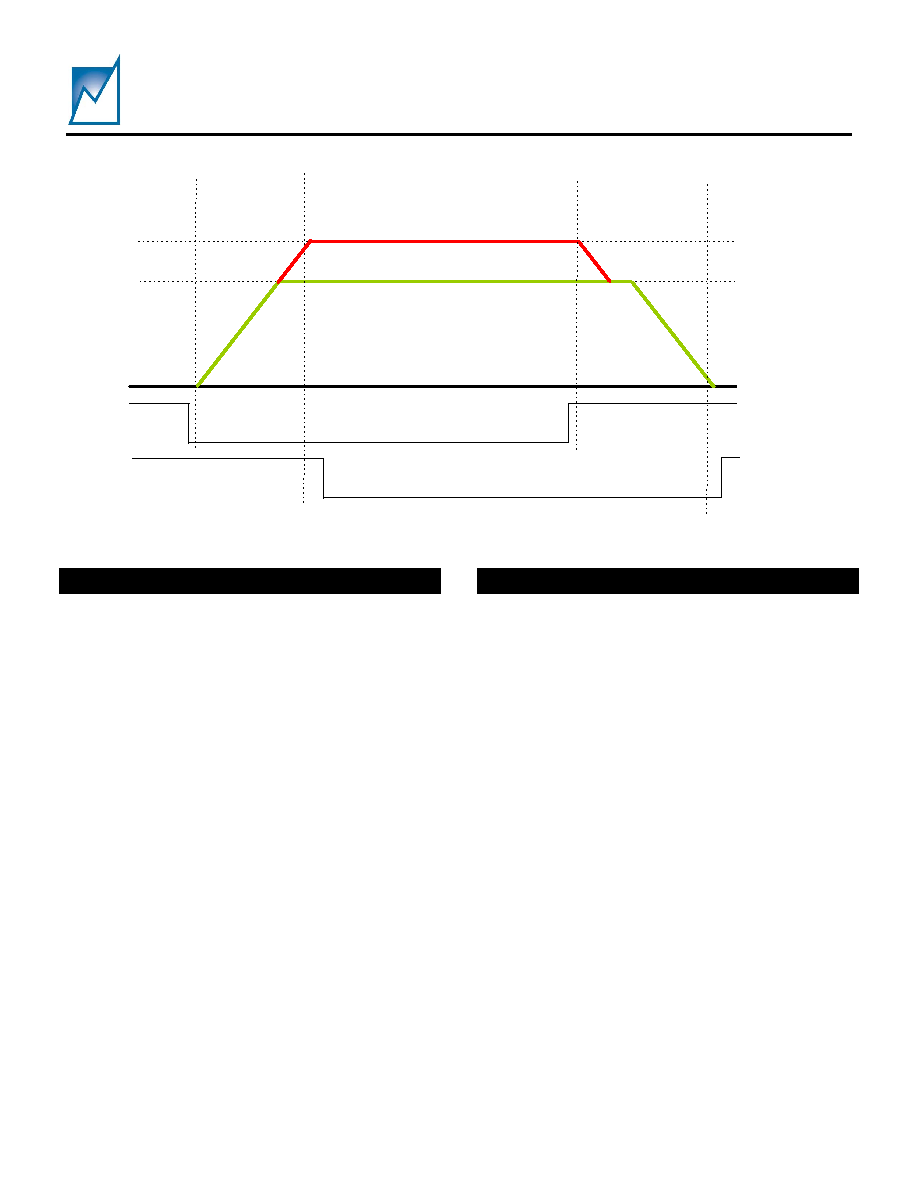
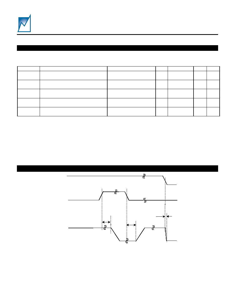
Figure 2 ≠ Typical Track Up and Track down waveform and the relationship of the PWR_ON# and
STATUS# pin functions
2.5V
1.5V
STATUS#
PW R_O N#
SMT2002
Preliminary Information
Summit Microelectronics, Inc
2063 4.2 1/23/03
3
TRACKING
During tracking the card-side voltages are
monitored to minimize the differential voltage between
the VOUTX pins until they reach their respective
thresholds.
In the tracking mode the VOUTX slew rates are
adaptive, with a maximum rate of 500V/s. If there is
any voltage difference between the VOUTX pins the
part will slow the 500V/S slew rate of the faster VOUT.
The VGATE outputs are adjusted so as to minimize
the voltage differential between VOUTA and VOUTB.
POWER-ON
The power-on operation is initiated by taking the
PWR_ON# pin low. Normally this pin should be pulled
low after the device receives power to both channels
on the bus side. However, it can be hardwired using a
simple delay circuit for automatic power-on in
standalone applications.
Once the power-on operation is initiated the
SMT2002 will begin tracking after time t
PWRON
. The
tracking operation ends when the VGATE outputs of
the tracking channels ramp up to their maximum
voltage and VOUTX is within 200mV of VINX.
To power-on, the FS# pin must be high. If FS# is
low the SMT2002 will not power on.
POWER-OFF
Once the SMT2002 has completed the power-on
operation the power-off operation can be initiated by
bringing the PWR_ON# pin high, which will initiate a
track down. Once the power-off operation is initiated
there is a delay of t
TRKDN
= VDD/(500V/s). At this point
the SMT2002 will begin discharging of the VGATE
output of the highest tracked channel. Once the
VOUTX inputs of both channels are within 100mV of
ground both VGATE outputs will be clamped to
ground.
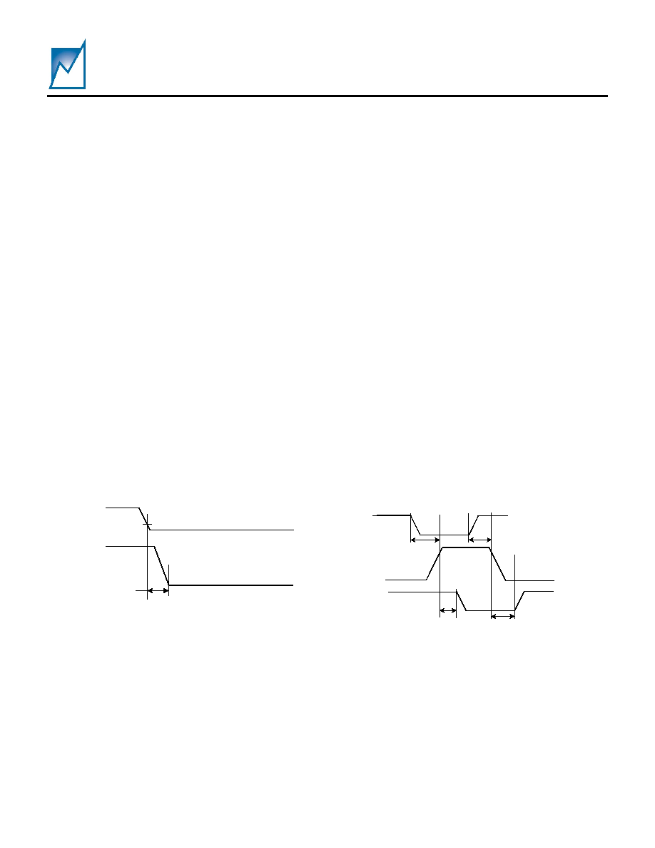
FORCE SHUTDOWN (See Figure 3)
The force shutdown function is initiated
externally. If the FS# pin is taken low the VGATE
outputs will immediately be clamped to ground after
the t
DFSVG
delay time.
STATUS OUTPUT (See Figure 4)
During power-on the STATUS# output will be
high until both managers detect their respective
VOUTX pins are within 200mV of the VINX pins and
the track up function is complete. STATUS# will
remain active low after the track up function is
complete and stay active until the track down function
is complete, and then go high.
Figure 4. Timing relation between STATUS# and
VGATEx
VG ATEx
STATUS#
t
STRKDN
t
STRKUP
PW R_O N#
t
PW RON
t
PW ROFF
VG ATEx
FS#
t
DFSVG
Externally triggered FS# action
Figure 3. Timing relation between FS# and VGATE
SMT2002
Preliminary Information
Summit Microelectronics, Inc
2063 4.2 1/23/03
4
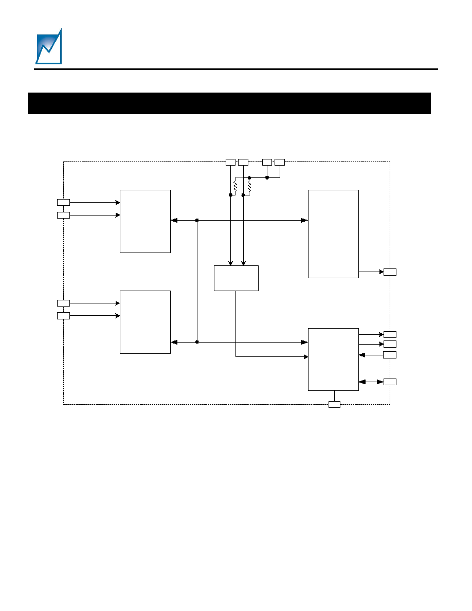
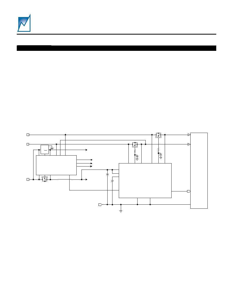
TRACKING
M ANAG ER
A
TRACKING
M ANAG ER
B
S TATUS
REG ISTE R
CHARG E
PUM P & V G ATE
CO NTRO L
VDD
SE Q UENCE
ENABLE
LO G IC
VG ATE A
VG ATE B
VG G _CAP
STATUS #
9
8
PW
R_
O
N
#
FS
#
12
11
10
3
14
GN
D
4
5
VINA
VO UTA
6
7
VINB
VO UTB
VG ATE V
1
2
R
PU LL-U P
VDD
13
NOTE1 ≠ Pin numbers are for the 14 pin SOIC
INTERNAL FUNCTIONAL BLOCK DIAGRAM
SMT2002
Preliminary Information
Summit Microelectronics, Inc
2063 4.2 1/23/03
5
Pin
Number
1
Pin
Type
Pin Name
Pin Description
1 I VGATEV
Controls Vgate1 and Vgate2 maximum output voltage level. If High VGATEX
= 14V, if Low VGATEX = 10V
2 PWR VDD VDD provides the positive supply voltage. It may range from 2.7V to 5.5V, but
must be greater than the highest tracked voltage.
3 I/O
VGG_CAP
Charge storage pin for internal VGATE VGG voltage. A 100nF to 1uF
capacitor rated to at least 16V must be attached to this pin.
4 I VINA
Bus side input channel A.
5 I VOUTA
Card side input channel A.
6 I VINB
Bus side input channel B.
7 I VOUTB
Card side input channel B.
8 I
PWR_ON#
Power on input to begin tracking or to track down. Active low. A 100k
internal pull-up resistor.
9 I FS# Force Shutdown input. Active low. 100k internal pull-up resistor.
10 O VGATEB
VGATE output for channel B.
11 O VGATEA
VGATE output for channel A.
12 O STATUS#
Indicates the state of VOUTA and VOUTB. Will go low when track up is
complete, and return high when track down is complete.
13
2
VDD VDD VDD provides the positive supply voltage. It may range from 2.7V to 5.5V, but
must be greater than the highest tracked voltage.
14 PWR GND GND is the lowest potential supply.
NOTE1 ≠ Pin numbers are for the 14 pin SOIC
NOTE2 ≠ Pin 13(15) was originally an NC (No Connect) pin for product marked with Status Tracking Code 01 (see Part Marking on the last page). For
product marked status tracking code 02, it is now a VDD pin. Connect pin 13(15) to pin 2 and also to a 0.1uF capacitor to ground (see Figure 8).
PIN DESCRIPTIONS
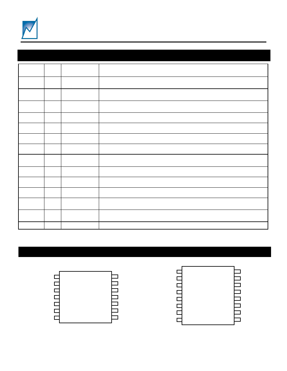
14 Lead SOIC
ST AT US#
FS#
VG AT EA
VDD
VG AT EB
SM T2002
VO UT B
VG G _CAP
VG AT EV
VO UT A
VINA
PW R_O N#
G ND
VINB
PIN 1
8
VDD
PACKAGE PIN CONFIGURATION
ST AT US#
FS#
VGAT EA
VDD
VGAT EB
SM T2002
VOUT B
VGG _CAP
VGAT EV
VOUT A
VINA
PW R_O N#
G ND
VINB
PIN 1
9
VDD
NC
NC
16 Lead SSOP
SMT2002
Preliminary Information
Summit Microelectronics, Inc
2063 4.2 1/23/03
6
ABSOLUTE MAXIMUM RATINGS
Temperature Under Bias .................... -55
∞
C to +125
∞
C
Storage Temperature.......................... -65
∞
C to +150
∞
C
Terminal Voltage with Respect to GND:
VIN & VOUT Inputs ..............GND-0.3V to.VDD+0.3V
VGATE
Outputs...............................................16V
All Others ............................................-0.3V to 7.0V
Output Short Circuit Current ...........................100mA
Lead Solder Temperature (10 secs)..................300
∞
C
Junction Temperature.........................................150∞C
ESD Rating per JEDEC................................2000V
Latch-Up testing per JEDEC.....................+/- 100mA
RECOMMENDED OPERATING CONDITIONS
Temperature Range (Industrial)......... ≠40
∞
C to +85
∞
C*
(Commercial) .......... ≠5
∞
C to +70
∞
C*
VDD Supply Voltage .................................. 2.7V to 6.0V
VIN & VOUT.............................................. GND to VDD
Package Thermal Resistance (
JA
)
14 Lead SOIC........................................80
o
C/W
16 Lead SSOP.......................................80
o
C/W
Moisture Classification Level 1 (MSL 1) per J-STD- 020
* Ambient
Note: The device is not guaranteed to function outside its operating
rating. Stresses listed under Absolute Maximum Ratings may cause
permanent damage to the device. These are stress ratings only and
functional operation of the device at these or any other conditions
outside those listed in the operational sections of the specification is
not implied. Exposure to any absolute maximum rating for extended
periods may affect device performance and reliability. Devices are
ESD sensitive. Handling precautions are recommended.
DC OPERATING CHARACTERISTICS
(Over recommended operating conditions, unless otherwise noted. All voltages are relative to GND.)
Symbol
Parameter
Notes
Min.
Typ.
Max
Unit
VDD
Supply Voltage
Device supply voltage
2.7
5.5
V
I
DD
(ON)
Power Supply Current
Active Current with
VGATEs enabled
3
mA
VGATE characteristics
VGATEV pin low
10
V
V
VGATE
VGATE output voltage
VGATEV pin high
14
V
V
VGATE
OFF
VGATE Output
I
VGATE
= 2mA
0
0.4
V
I
VGATE
VGATE Drive Current
VGATE = 5V
5
20
µA
SR
VGATE
VGATE Slew Rate
500
V/S
V
TRKR
Tracking Differential Voltage
Allowable differential
between VOUT pins
100
250
mV
All other input and output characteristics
VDD = 2.7V
0.9xVDD
VDD
V
V
IH
Input High Voltage
VDD = 5.0V
0.7xVDD
VDD
V
VDD = 2.7V
-0.1
0.1xVDD
V
V
IL
Input Low Voltage
VDD = 5.0V
-0.1
0.3xVDD
V
V
OL
Open Drain Output (Status)
I
SINK
= 2mA
0
0.4
V
R
VI,VO
Input Resistance from VIN or VOUT to
GND
140
k
R
Pull-Up
Input Pullup Resistors
See Pin Descriptions
50
100
165
k
SMT2002
Preliminary Information
Summit Microelectronics, Inc
2063 4.2 1/23/03
7
AC OPERATING CHARACTERISTICS
(Over recommended operating conditions and VGG_CAP fully charged, unless otherwise noted. All voltages
are relative to GND.) See Figure 3, 4 and 5 Timing diagrams.
Symbol Description
Conditions
Min
Typ
Max
Unit
t
PWRON
Delay from PWR_ON# valid to
VGATEX activated
VGATEX activated at
85% of VGG_CAP level
8
ms
t
PWROFF
Delay from PWR_ON# not valid to
VGATEX deactivated
VGATEX deactivated at
85% of VGG_CAP level
VDD/(500V/s)
s
t
STRKUP
Delay from VGATEX activated to
STATUS# activated
VGATEX activated at
85% of VGG_CAP level
10
ms
t
STRKDN
Delay from VGATEX deactivated to
STATUS# deactivated
VGATEX deactivated at
85% of VGG_CAP level
10
ms
t
DFSVG
Delay from assertion of FS# to
VGATE clamped to ground.
VGATE Capacitance =
10nF
100
µs
PW R_O N#
VG ATEs
FS#
t
DFSVG
t
PW RON
t
PW ROFF
Figure 5 - Timing relationship of de-asserting the enabling inputs on the VGATE outputs
TIMING DIAGRAMS
SMT2002
Preliminary Information
Summit Microelectronics, Inc
2063 4.2 1/23/03
8
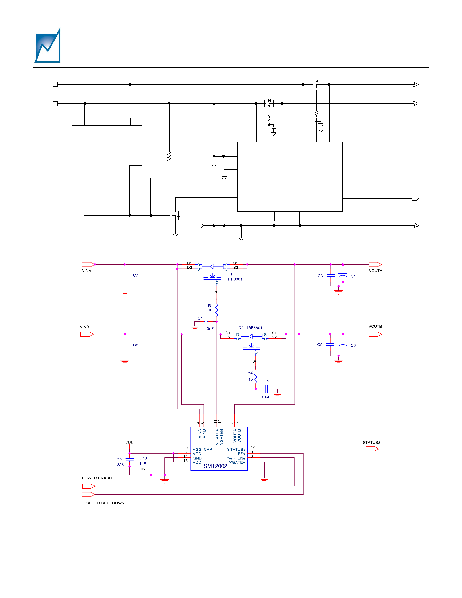
APPLICATIONS INFORMATION
The SMS64 and SMT2002 can be used together to
power and provide Status, Reset and IRQ control of
the Network Processor system as shown in Figure 6.
The tracker function can be used by a single
processor and peripheral ICs or by two processors.
Figure 7 shows a low cost power management
solution consisting of the SMS24 and SMT2002.
Figure 8 shows the SMT2002 in a standalone
design and recommended external components. The
VGATE output pins require series resistors to drive the
gates of the power MOSFETs. Gate capacitors are
always recommended to prevent initial MOSFET turn-
on before the SMT2002 initializes the power on
sequence. To minimize transient power surges in hot-
swappable line card designs, place a 0.01
µF (10nF),
25V, ceramic capacitor on each VGATE output pin to
ground.
The VGATE output level is selectable to either
10V or 14V, depending on the type of MOSFET. To
minimize the voltage drop across the MOSFET it
needs to be fully enhanced to minimize RDS
(ON)
.
However, some MOSFETs have maximum V
GS
specifications of 15V while others are 20V. For
improved tracking performance with the SMT2002 it is
recommended to use the lower rated VGS devices
with the VGATE output levels set to 10V instead of
14V. The VGATEV pin must be low to set the VGATE
outputs to 10V. The industry trend for power
MOSFETs is toward lower V
GS
voltages while also
reducing RDS
(ON)
specifications.
+3.3V
S M S 64
VCC
B
PUP
B
VM
B
VM
C
VCC
A
PUP
A
VM
A
PUP
C
+1.3V
+3.3V O U T
+2.5V O U T
+1.5V
VCC
D
VCC
C
10n F
10
V D D
V G G _C AP
P W R _O N #
G N D
V G ATE V
S TATU S #
S M T2002
VI
NA
VG
A
T
EA
VI
NB
VG
A
T
EB
1µF
1.5V O U T
1.3V O U T
G N D
S TATU S #
VO
UT
A
VO
UT
B
G N D
V+
O U T
O N /O FF
R S T_A#
IR Q #
R S T_A#
R S T_B #
R S T_B #
IR Q #
10n F
10
Network
Processor
V D D
0.1µF
Figure 6 - SMT2002 two-channel Trakker
TM
used with the SMS64 Sequencer (Not all components shown, see
Figure 8).
SMT2002
Preliminary Information
Summit Microelectronics, Inc
2063 4.2 1/23/03
9
Figure 7 - SMT2002 two-channel Trakker
TM
used with the SMS24 Sequencer (Not all components shown, see
Figure 8).
Figure 8 - SMT2002 standalone two-channel Trakker
TM
(R1 and R2 are series MOSFET gate termination
resistors, C1 and C2 are for charge control and to hold the MOSFET gates low until the SMT2002 powers up,
C4 and C6 are bulk capacitance, C3, C5, C7, C8 and C9 are noise bypass capacitors, C10 is the charge pump
capacitor). Pin numbers are for the 14 pin SOIC.
SM S24
R
E
SET
#
+1.8VIN
+3.3VIN
VS
EN
S
E
VC
C
10nF
10
VDD
VG G _CAP
PW R_O N#
G ND
VG ATEV
STATUS #
SM T2002
VI
N
A
VG
A
T
EA
VI
N
B
VG
A
T
EB
1µF
3.3VO UT
1.8VO UT
G ND
G ND
STATUS #
VO
U
T
A
VO
U
T
B
VL
O
W
#
50K
10nF
10
VDD
0.1µF
SMT2002
Preliminary Information
Summit Microelectronics, Inc
2063 4.2 1/23/03
10
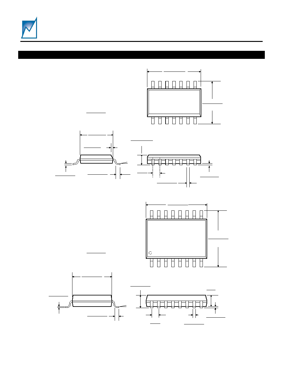
PACKAGE
14 Lead SOIC Package
0.150 - 0.157
0.013 - 0.020
(0.33 - 0.51)
0.004 - 0.01
(0.10 - 0.25)
0.337 - 0.344
(8.55 - 8.75)
0.228 - 0.244
(5.80 - 6.20)
0.053 - 0.069
(1.35 - 1.75)
0.016 - 0.050
(0.40 - 1.27)
(1.27)
0.0075 - 0.01
(0.19 - 0.25)
0.01 - 0.02
(0.25 - 0.50)
(3.80 - 4.00)
14 Pin SOIC
◊45∫
0.016 - 0.050
0.05
0 to 8
typ
1
Ref. JEDEC MS-012
Inches
(Millimeters)
16 Lead SSOP Package
0.007 - 0.010
(0.18 - 0.25)
0.150 - 0.157
(3.81 - 3.99)
0.025
(0.635)
0.016 - 0.050
(0.41 - 1.27)
0.008 - 0.012
(0.20 - 0.31)
0.189 - 0.197
(4.80 - 5.00)
0.228 - 0.244
(5.79 - 6.20)
Pin 1
0∫ to 8∫
0.004 - 0.010
(0.10 - 0.25)
0.059
(1.50)
0.053 - 0.069
(1.35 - 1.75)
MAX
16 Pin SSOP
Ref. JEDEC MO-137
Inches
(Millimeters)
SMT2002
Preliminary Information
Summit Microelectronics, Inc
2063 4.2 1/23/03
11
PART MARKING
SM T2002S
AYYW W
Pin 1
C
Sum m it Part N um ber
Date Code (YYWW)
Product Tracking Code
(Summit use)
(C = Commercial Temperature
Range)
Lot tracking code (Summit use)
Drawing not to scale
xx
Status Tracking Code
(Summit Use)
SUM M IT
ORDERING INFORMATION
NOTICE
NOTE 1 - This is a Preliminary Information data sheet that describes a Summit product currently in pre-production with limited characterization.
SUMMIT Microelectronics, Inc. reserves the right to make changes to the products contained in this publication in order to improve design,
performance or reliability. SUMMIT Microelectronics, Inc. assumes no responsibility for the use of any circuits described herein, conveys no
license under any patent or other right, and makes no representation that the circuits are free of patent infringement. Charts and schedules
contained herein reflect representative operating parameters, and may vary depending upon a user's specific application. While the information in
this publication has been carefully checked, SUMMIT Microelectronics, Inc. shall not be liable for any damages arising as a result of any error or
omission.
SUMMIT Microelectronics, Inc. does not recommend the use of any of its products in life support or aviation applications where the failure or
malfunction of the product can reasonably be expected to cause any failure of either system or to significantly affect their safety or effectiveness.
Products are not authorized for use in such applications unless SUMMIT Microelectronics, Inc. receives written assurances, to its satisfaction, that:
(a) the risk of injury or damage has been minimized; (b) the user assumes all such risks; and (c) potential liability of SUMMIT Microelectronics, Inc.
is adequately protected under the circumstances.
This document supersedes all previous versions. Please check the Summit Microelectronics Inc. web site at
www.summitmicro.com
for data
sheet updates.
© Copyright 2003 SUMMIT MICROELECTRONICS, Inc.
Power Management for CommunicationsTM