 | –≠–ª–µ–∫—Ç—Ä–æ–Ω–Ω—ã–π –∫–æ–º–ø–æ–Ω–µ–Ω—Ç: SMT4004A | –°–∫–∞—á–∞—Ç—å:  PDF PDF  ZIP ZIP |
SMT4004A
©
Summit Microelectronics, Inc.
2003
∑
300 Orchard City Drive, #131 ∑ Campbell CA 95008
∑ Phone 408 378-6461 ∑ FAX 408 378-6586 ∑
www.summitmicro.com
2072 1.0 8/27/03
1
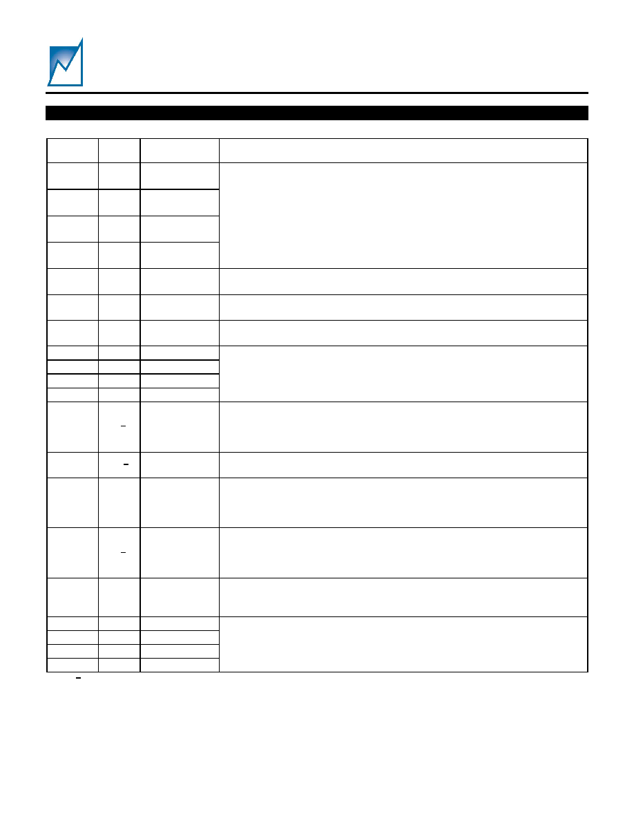
FEATURES & APPLICATIONS
∑ 1% OV and UV Threshold Accuracy
∑ Programmable Softstart, Tracking and Voltage
Monitoring Functions
∑ Controls 4 Independent Supplies Down to 0.9V
Programmable Bus-Side and Card-Side UV and
OV Thresholds
∑ Guarantees Differential Supply Tracking
∑ Operates From Any One of Four Supply
Voltages down to 2.7V
∑ Four independent RST#s, two IRQ#s,
CROWBAR and Circuit breaker functions
∑ I
2
C 2-Wire Serial Bus Interface for Program-
ming, Power On/Off and Operational Status
∑ 256X8 Nonvolatile EEPROM Memory Array
Applications
∑ Power Supply Management
∑ Telecom/Datacom Motherboards/Servers
∑ Mezzanine Line Cards
∑ Compact
PCI
TM
Hot Swap Control
∑ Network Processors, DSPs, ASICs
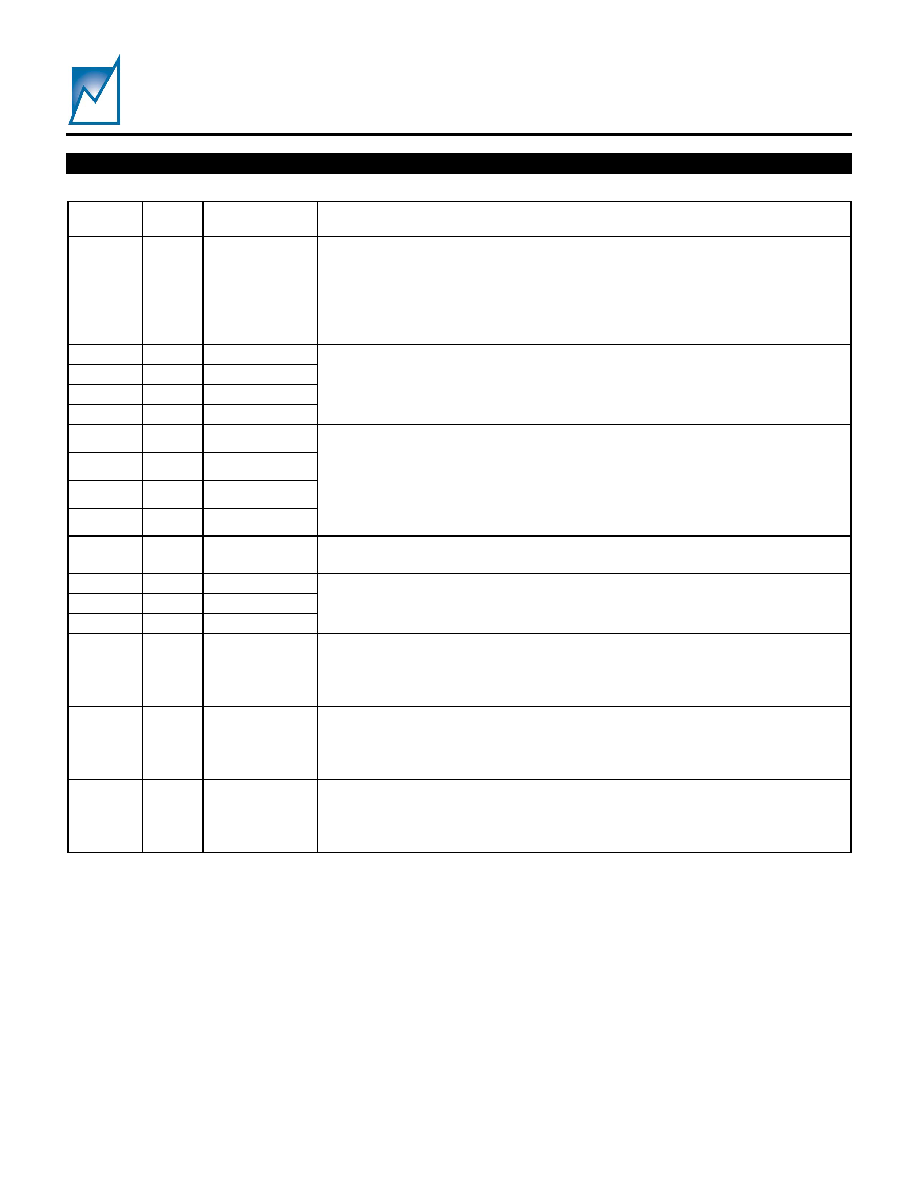
INTRODUCTION
The SMT4004A trakker
tm
is a fully integrated
programmable voltage manager IC, providing
precision accuracy (
±1%) supervisory functions and
tracking control for up to four independent power
supplies. The four internal managers perform the
following functions: monitor source (bus-side) voltages
for under-voltage and over-voltage conditions, monitor
back end (card-side) voltages for under-voltage
conditions, ensure voltages to the card-side track
within specified parametric limits, and provide status
information to a host processor.
The SMT4004A incorporates nonvolatile program-
mable circuits for setting all monitored thresholds for
each manager. Individual functions are also pro-
grammable allowing Interrupts or Reset conditions to
be generated by many combinations of events. Also
included are nonvolatile fault status registers and a
2K-bit (256 byte) nonvolatile memory.
User programming of configuration and control values
is simplified with the interface adapter (SMX3200) and
Windows GUI software obtainable from Summit
Microelectronics.
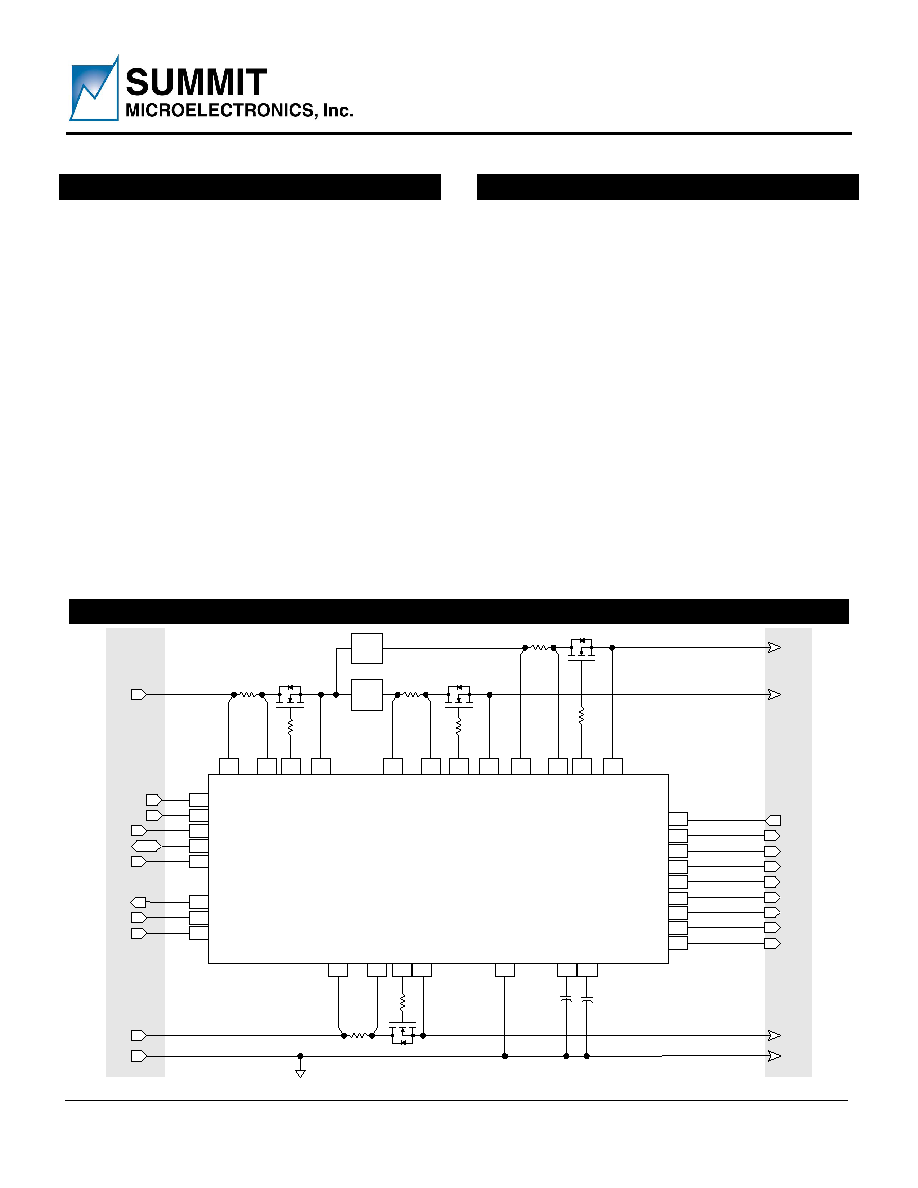
Bus-
S
i
de C
onnect
o
r
C
a
r
d
-
S
i
de A
ppli
c
at
ion
C
i
r
c
ui
t
s
2.5V
10
1.5V
10
10
SMT4004A
10
SCL
SDA
SEATED1#
SEATED2#
ENABLE
PWR_ON
HEALTHY#
IRQ_CLR#
GND
VI
2
CB2
VGA
T
E2
VO
2
V
GG_C
A
P
V
DD_CAP
VI
1
CB
1
VGA
T
E1
VO1
VI
3
CB3
VGA
T
E3
VO3
VI
4
CB4
VGA
T
E
4
VO
4
1uF
10µF
RST1#
RST2#
RST3#
RST4#
IRQ#
TRKR_IRQ#
MR#
WDO#
LDO#
RS
1
RS
2
RS
4
RS
3
41
37
32
20
39
35
30
22
34
29
23
38
5
1
2
7
9
13
14
15
16
28
42
18
36
31
21
40
26
6
33
10
11
47
46
24
Note: This is an applications example only. Some pins, components and values are not shown.
QUAD TRAKKING
TM
POWER SUPPLY MANAGER WITH 1% UV/OV THRESHOLD ACCURACY
SIMPLIFIED APPLICATIONS DRAWING
SMT4004A
Summit Microelectronics, Inc
2072 1.1 3/7/03
2
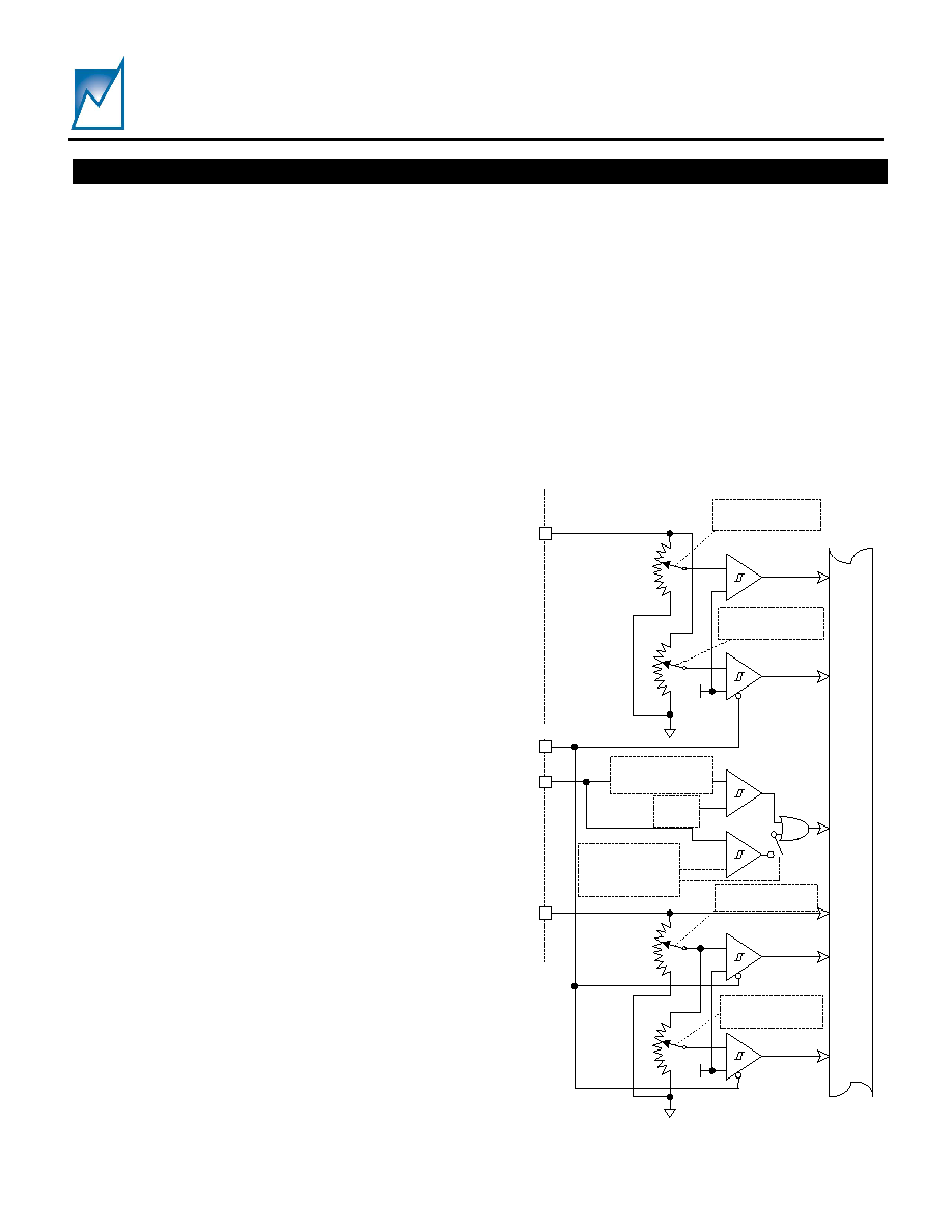
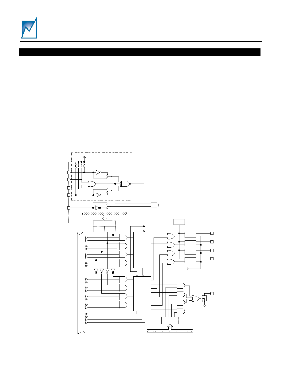
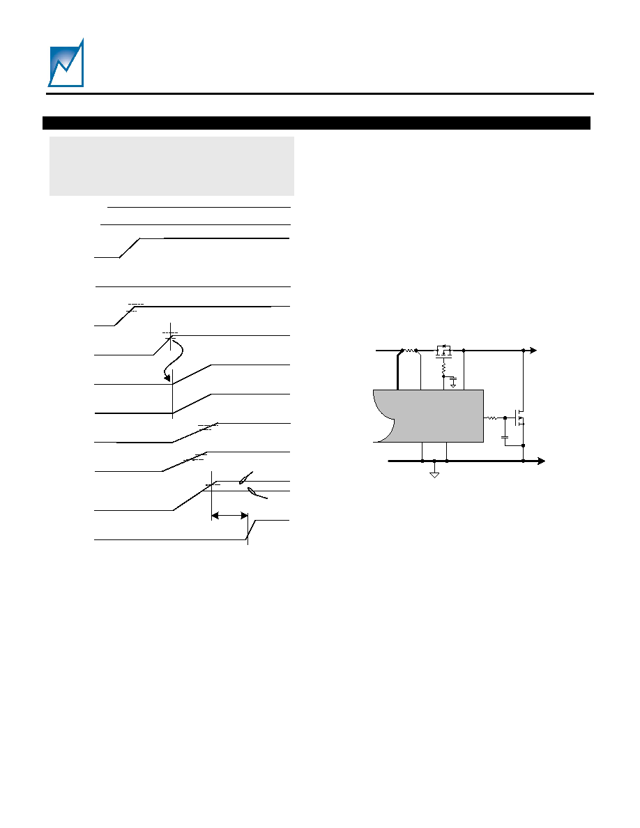
SUPPLY MANAGERS
The SMT4004A has four distinct programmable power
supply managers and associated circuitry (see Figure
7). The managers are individually programmable and
can operate independently or together with the other
managers. Each manager monitors the bus and card-
side voltages and current for that supply (Figure 1).
The VI pin is the bus-side input that connects to two
comparators to monitor under-voltage (UV) and over-
voltage conditions (OV). The threshold for the UV
detector is programmable in 20mV increments, from
0.9V to 6.0V. The OV detector is programmable in 4%
increments of the UV settings, from 120% to 244% of
the UV settings. The OV threshold is an offset from
the UV sensor and the offset varies as the UV
threshold: if UV is set to 0.9V then OV can be set
from 1.08 to 2.2V.
The OV setting is related to the UV setting according
to the formula:
OV = UV X [(0.04 X DecVal) + 1.2]
Where: OV = Bus-side Over-voltage setting, UV =
Bus-side Under-voltage setting, and DecVal = Decimal
value of OV Register contents.
If the VI input is below the UV threshold the manager
generates a UV fault status on the internal bus. If the
VI input is above the OV threshold the manager
generates an OV fault status on the internal bus. The
UV and OV status information can be selected to
generate an IRQ# output. Refer to Figure 3 for an
illustration of the IRQ# function and the relation of the
UV and OV status of the four managers.
The VO pin is the card-side input that connects to two
comparators to monitor two under-voltage threshold
conditions. The threshold for the first under-voltage
monitor (UV1) is programmable in 20mV increments,
from 0.9V to 6.0V. If the VO input is below the UV1
threshold the manager generates an UV1 fault status
on the internal bus.
The threshold for the second under-voltage monitor
can be set equal to the UV1 threshold or to one of 31
values less than UV1. The UV2 setting is related to
the UV1 setting according to the formula:
UV2 = UV1 X [1-(0.01 X DecVal)]
Where: UV1 = Card-side primary Under-voltage
setting, UV2 = Card-side secondary Under-voltage
setting, and DecVal = Decimal value of UV2 Register
contents (last 5 LSBs).
If the VO input is below the UV2 threshold the
manager generates an UV2 fault status on the internal
bus. Generally the first threshold, UV1, is used to
provide a warning that the supply is deteriorating while
the second threshold, UV2, is set lower to indicate the
supply is out of the operating range. The UV1 and
UV2 status outputs from the manager can be
programmed to generate a Reset or an Interrupt.
DETAILED DEVICE DESCRIPTION
VI
CB
Programmable
Offset
-
+
V
REF
-
+
-
+
V
REF
-
+
-
+
25mV
50mV
Programmable
Delay
Programmable
QuickTrip
Threshold
QT-CB
VO
OV
UV
UV1
UV2
VO
Programmable
Threshold
Programmable
Offset
-
+
Inter
n
a
l
Bus
UV_OVERRIDE
Programmable
Threshold
Figure 1. Supply Manager Schematic.
SMT4004A
Summit Microelectronics, Inc
2072 1.1 3/7/03
3
The UV_OVERRIDE input is used to mask under-
voltage conditions. When asserted (high) all under-
voltage conditions are ignored. This function is used
either during system test or when performing voltage
margin tests. During normal operation this pin must
be connected to ground.
CB is the circuit breaker input. A series resistor
placed between VI and CB causes the circuit breaker
to trip when the voltage across the resistor exceeds
the programmed value of 25mV or 50mV (V
CB
). A
programmable filter is provided to allow voltage drops
greater than V
CB
for selected delays of 25µs, 50µs,
100µs or 200µs. If the filter time is exceeded an over-
current condition (QT-CB) is generated from the
manager.
The CB pin is also connected to the QuickTrip
comparator. It is used in conjunction with the circuit
breaker function or may be disabled. When enabled,
a voltage across the series resistor exceeding the
QuickTrip threshold (V
QT
) instantly generates a QT-CB
signal from the manager. V
QT
can be set to different
levels depending on the CB selection. See V
QT
page
13.
The QT-OC output from the manager can generate a
RST# (Figure 2), an IRQ#, (Figure 3) or an internal
force shutdown (FSD) and crowbar output (Figure 5).
DEVICE POWER SUPPLY
The VI inputs also provide the operating supply
voltage for the SMT4004A. Internally they are diode-
ORed, so the highest potential VI input becomes the
VDD supply. Refer to the functional Block Diagram on
page 8.
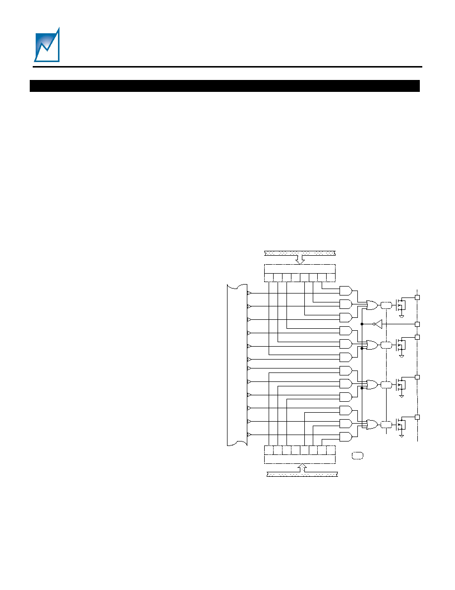
RESET CIRCUIT
The SMT4004A has four active-low, open-drain Reset
pins (RST1# - RST4#). All RST# outputs are asserted
once power is applied; remaining asserted for t
PRTO
(programmable reset timeout period, Figure 10) after
all Reset generating conditions are removed.
Individual RST# outputs can be programmed to
become active from three manager status conditions:
UV1, UV2 or QT-CB. The RST# output remains active
for t
PRTO
after the fault condition is removed (Figure 2).
Asserting the Manual Reset input (MR# low) forces all
RST# outputs low. The RST# outputs remain low
while MR# is low, returning high t
PRTO
seconds after
MR# is de-asserted.
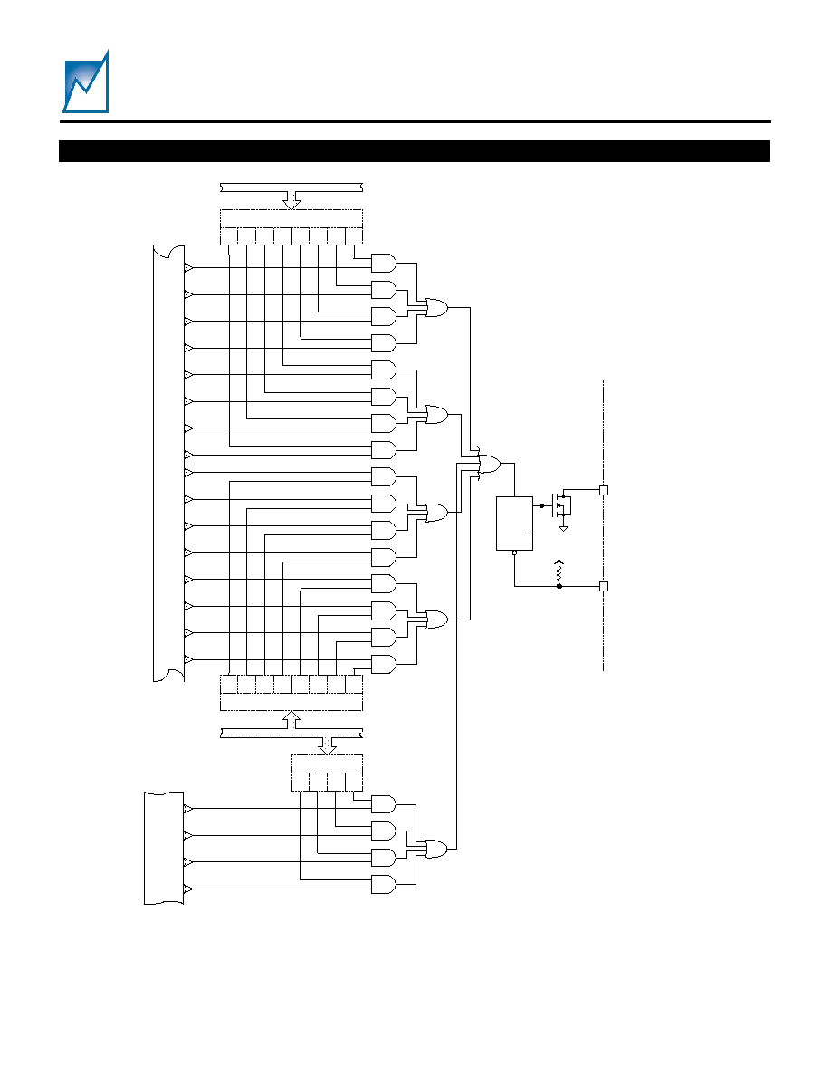
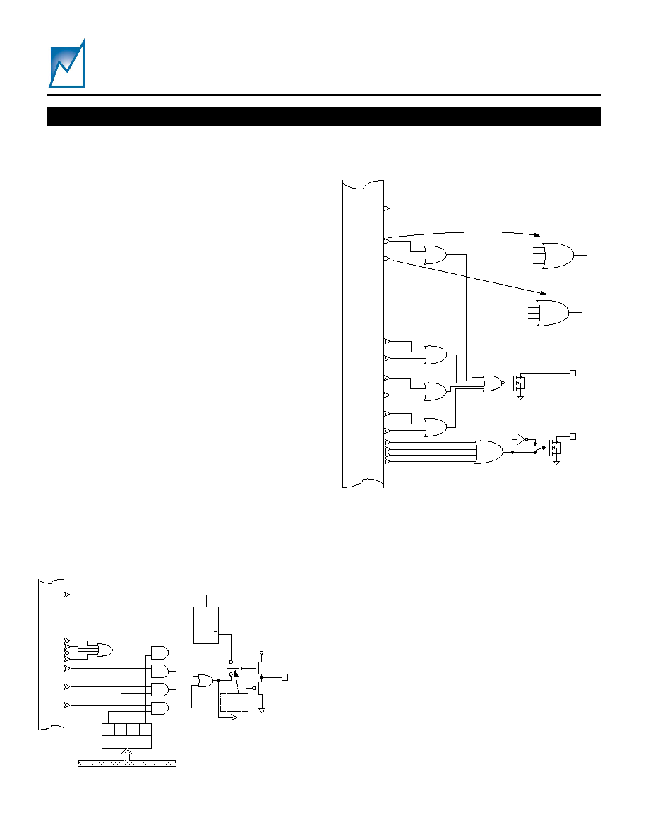
INTERRUPT (IRQ#) CIRCUIT
The SMT4004A has an active-low open-drain IRQ#
output. The sources for triggering an interrupt are
selected from the UV, OV, UV1 and UV2 status
outputs of each manager. When asserted, IRQ# is
latched and can only be cleared by a high to low
transition on the IRQ_CLR# pin (Figure 3).
0
1
2
3
4
5
6
7
RESET & TRKR_IRQ SELECT REG
0
1
2
3
4
5
6
7
RESET & TRKR_IRQ SELECT REG
UV2
2
UV1
2
UV2
1
UV1
1
UV2
3
QT-CB
3
UV1
3
UV2
4
UV1
4
RST2#
RST1#
RST3#
RST4#
reset circuit
PRT
PRT
MR#
PRT
Programmable Reset Timer
QT-CB
4
QT-CB
1
QT-CB
2
PRT
PRT
Figure 2. Programmable and hard-wired sources for
generating resets.
DETAILED DEVICE DESCRIPTION
(CONTINUED)
SMT4004A
Summit Microelectronics, Inc
2072 1.1 3/7/03
4
QT_CB
1
IRQ#
0
1
2
3
4
5
6
7
IRQ# SELECT REGISTER
UV2
2
UV1
2
UV
2
OV
2
UV2
1
UV1
1
UV
1
OV
1
UV2
4
UV1
4
UV
4
OV
4
UV2
3
UV1
3
UV
3
OV
3
SET
RESET
Q
Q
IRQ_CLR#
VDD_CAP
0
1
2
3
IRQ# SELECT
REGISTER
0
1
2
3
4
5
6
7
IRQ# SELECT REGISTER
QT_CB
2
QT_CB
3
QT_CB
4
Figure 3. Interrupt sources from the SMT4004A supply managers.
DETAILED DEVICE DESCRIPTION
(CONTINUED)
SMT4004A
Summit Microelectronics, Inc
2072 1.1 3/7/03
5
Active Low
Active High
Active Low
Active High
SEATED1#
PW R_ON
SEATED2#
FORCE_SD
VDD_CAP
100K
4 plcs
VG
1
VG
2
VG
3
VG
4
Tracker Select
Regs
UV
1
OV
1
UV
2
OV
2
UV
3
OV
3
UV
4
OV
4
UV
1
OV
1
UV
2
OV
2
UV
3
OV
3
UV
4
OV
4
Active Low
Active High
ENABLE
SEQUENCE
ENABLE
LOGIC
VGATE
Circuit
VGATE
Circuit
VGATE
Circuit
VGATE
Circuit
Charge
Pump
VGATE
CONTROL
SOFTSTART
VGATE
CONTROL
TRACKING
DONE
VGATE1
VGATE2
VGATE3
VGATE4
VO
1
VO
2
VO
3
VO
4
TRKR_IRQ#
TRKR_IRQ
SELECT
T RKR
3
TRKR
1
TRKR
4
TRKR
2
FSD
Figure 4. Charge Pump and VGATE Control
CHARGE PUMP AND VGATE CONTROL
The VGATE outputs control the gate voltages of
external N-channel MOSFETs. Each MOSFET
separates the bus and card-side voltages. The
VGATE outputs control the card-side slew rates during
the power-on/-off interval. The VGATEs are turned on
when their controlling inputs either meet softstart
conditions or when tracking conditions are met so the
MOSFET card-side voltages track. The manager
inputs (Figure 1) and the control inputs (Figure 4)
control the VGATE outputs.
Certain conditions must be met for the VGATE outputs
to become active. The conditions are defined by the
sequence enable logic, the manager inputs and the
user selected function (softstart or track) for each
VGATE output.
The VGATE control blocks (Figure 4) are the logic
functions controlling the VGATE outputs. All inputs to
these blocks are used to enable the VGATE outputs to
drive the external MOSFETs.
The ENABLE input only affects the charge pump
(VGG_CAP voltage). Its active state is programmable
and must be true to turn-on the charge pump. The
charge pump provides the high-side drive voltage to
the VGATE pins.
The PWR_ON and FORCE_SD inputs active states
are programmable. PWR_ON, SEATED1# and
SEATED2# must be true and FORCE_SD false to
enable a power-on sequence.
DETAILED DEVICE DESCRIPTION
(CONTINUED)
SMT4004A
Summit Microelectronics, Inc
2072 1.1 3/7/03
6
If both softstart and tracking are enabled, the softstart
VGATE outputs must be fully on (VGATE =
VGG_CAP) before the tracking VGATEs are enabled.
The VO inputs are monitored and compared by the
tracking logic to control the VGATEs of the tracked
voltages. They are also used by the VGATE tracking
control logic to generate a TRKR_IRQ# output if a
differential of
>300mV between any tracked VO input
occurs during the tracking interval.
FORCE SHUTDOWN AND CROWBAR
The VGATE outputs can be rapidly shutdown by
asserting the FORCE_SD input or when an internally
generated force shutdown (FSD) occurs.
Internal sources that generate a force shutdown are
programmable and are: a TRKR_IRQ#, a general
IRQ# or an over-current condition (QT-CB) (Figure 5).
HEALTHY# AND CBFAULT
The SMT4004A has two status output pins,
HEALTHY# and CBFAULT (Figure 6). HEALTHY# is
an active-low open-drain output that is asserted when
all bus and card-side conditions are within the
programmed settings, i.e., there must be no bus or
card-side fault conditions (programmed RST#s,
IRQ#s, or TRKR_IRQ#s) from the bus-side UV, OV
and card-side UV1, UV2 and QT-CB outputs from the
managers. If no RST#s, IRQ#s, or TRKR_IRQ#s are
enabled, HEALTHY# will stay asserted even if fault
conditions exist. HEALTHY# is an instantaneous
indication of the status of the RST#s, IRQ#, and
TRKR_IRQ# signals, and is derived from the
unlatched versions of these signals. The CBFAULT is
programmable as an active high or active low output.
It is asserted when an over-current condition (QT-CB)
occurs (Figure 6).
FAULT STATUS REGISTERS
The SMT4004A has three nonvolatile fault status
registers. When an IRQ# is generated the cause of
the interrupt is recorded in the fault register. The fault
source is indicated as a `1' in the assigned bit location
(Table 1). The fault status registers are overwritten
each time an IRQ# is generated. The fault status
registers are always available for reading except for
when a nonvolatile write is in progress. Overwriting
(clearing) the fault condition is dependent upon the
device configuration with regard to the programmable
`active writing state' of the MR# input. Clearing the
fault status registers is not necessary as the last fault
condition overwrites any information previously stored.
If clearing the registers is desired, it is accomplished
by forcing a write to those registers while no fault
conditions exist.
FORCE_SD
REG
QT-CB
1
FORCE_SD
IRQ
TRKR_IRQ
CROWBAR
VDD_CAP
SET
RESET
Q
Q
CROWBAR
FUNCTION
SELECT
BEGIN_TRK
QT-CB
2
QT-CB
3
QT-CB
4
FSD
Figure 5. Force Shutdown (FSD) and CROWBAR circuitry.
HEALTH
CBFAULT
Card-Side UV1
X
Card-Side UV2
X
Bus-Side UV
X
Bus-Side OV
X
TRKR_IRQ
IRQ
X
Typical of All Channels
Card-Side UV1
X
Card-Side UV2
X
QT-CB
X
RST
X
RST
1
IRQ
1
RST
2
IRQ
2
RST
3
IRQ
3
RST
4
IRQ
4
QT-CB
1
QT-CB
2
QT-CB
3
QT-CB
4
Figure 6. HEALTHY# and CBFAULT circuitry.
DETAILED DEVICE DESCRIPTION
(CONTINUED)
SMT4004A
Summit Microelectronics, Inc
2072 1.1 3/7/03
7
For prototyping purposes, the Windows GUI
(described in the Serial Interface section) has an
option to clear the fault status registers.
Fault recording is disabled when the PWR_ON input is
de-asserted.
WATCHDOG AND LONGDOG TIMERS
The SMT4004A's internal timer triggers the activation
of the LDO# and WDO# outputs. LDO# and WDO#
are active-low open-drain outputs that can be wire-
ORed with other open-drain signals.
During a power-on sequence the timers are disabled
until all four Resets are released. At this time both
timers, if enabled, begin clocking at t
0
. If either times
out, it asserts its respective output. The timers work in
tandem, so any low to high transition on the WLDI
input Resets both timers to t
0
.
The longdog timer must be programmed to timeout
sometime after the watchdog timer. The WDO# could
then be wire-ORed with the IRQ# output to provide an
alert that action needs to be taken. The LDO# output
could be wire-ORed with a system RST# signal to
indicate a shutdown condition exists.
Both timers can be programmed off, facilitating system
debug. This feature can also be used to allow an
operating system to boot-up and configure itself
without Interrupts or Resets.
SERIAL INTERFACE AND GENERAL PURPOSE
EEPROM MEMORY ARRAY
The SMT4004A uses the industry standard I
2
C 2-wire
serial data interface. This interface provides access to
the configuration registers, the nonvolatile fault
registers and a 2K-bit (256 byte) nonvolatile memory.
The interface has three address inputs (A0, A1, and
A2) allowing up to eight devices on the same bus.
This allows multiple devices on the same board or
multiple boards in a system to be controlled with two
signals: SDA and SCL.
The configuration and nonvolatile fault registers share
the same device type identifier, 1001
BIN
, which is
distinct from the 2K-memory device type identifier,
optionally 1010
BIN
or 1011
BIN
. The separation of
address space allows full utilization of the EEPROM
memory array. The memory is functionally identical to
the industry standard 24C02. However, the last 48-
bytes in the memory array are reserved for test
purposes.
The memory array can be read with MR# low. The
memory array cannot be written when the part is in
reset whether from MR# being low or from any other
reset source. The configuration and fault registers
may be read regardless of the state of MR#. A user
option selects the active state of the MR# input for
writing to the configuration and fault registers.
Device configuration utilizing the Windows based
SMT4004A graphical user interface (GUI) is highly
recommended. The software is available from the
Summit website (
www.summitmicro.com
). Using the
GUI in conjunction with this datasheet and Application
Note 22 simplifies the process of device prototyping
and the interaction of the various functional blocks. A
programming Dongle (SMX3200) is available from
Summit to communicate with the SMT4004A. The
Dongle connects directly to the parallel port of a PC
and programs the device through a cable using the I
2
C
bus protocol.
DETAILED DEVICE DESCRIPTION
(CONTINUED)
7
6
5
4
3
2
1
0
UV
1
UV
2
UV
3
UV
4
OV
1
OV
2
OV
3
OV
4
7
6
5
4
3
2
1
0
TR
K
R
1
TR
K
R
2
TR
K
R
3
TR
K
R
4
QT
-
C
B
1
QT
-
C
B
2
QT
-
C
B
3
QT
-
C
B
4
7
6
5
4
3
2
1
0
UV
1
1
UV
1
2
UV
1
3
UV
1
4
UV
2
1
UV
2
2
UV
2
3
UV
2
4
Fault Status Register Address 1D
Fault Status Register Address 1E
Fault Status Register Address 1F
Table 1. Fault Status register bit allocation

SMT4004A
Summit Microelectronics, Inc
2072 1.1 3/7/03
8
INTERNAL BLOCK DIAGRAM
SUPPLY
M ANAGER
#1
SUPPLY
M ANAGER
#2
SUPPLY
M ANAGER
#3
SUPPLY
M ANAGER
#4
RESET
INTERRUPT
CONTROL
&
FAULT STATUS
REGISTERS
RST1#
13
14
CHARGE
PUMP & VGATE
CONTROL
TIM ER LOGIC
SERIAL
INTERFACE
&
MEM ORY
ARRAY
5
6
24
VDD_CAP
SEQUENCE
ENABLE
LOGIC
POWER SUPPLY
ARBITRATION
W LDI
LDO#
W DO#
SCL
SDA
A0
A1
A2
VGATE1
VGATE2
VGATE3
VGATE4
VGG_CAP
RST2#
RST3#
RST4#
IRQ#
TRKR_IRQ#
CBFAULT
CROW BAR
HEALTHY#
I
R
Q
_
CLR#
MR
#
EN
A
B
L
E
27
33
10
11
SE
A
T
ED
2
#
SE
A
T
ED
1
#
PW
R
_
O
N
F
O
R
C
E
_
S
D
15
16
7
9
3
26
25
32
31
30
29
28
48
1
2
47
46
43
44
45
8
17
18
19
42
PGN
D
PGN
D
DGND
AG
N
D
VD
D
_
C
A
P
41
20
37
VI1
VO1
CB1
40
21
36
VI2
VO2
CB2
39
22
35
VI3
VO3
CB3
38
23
34
VI4
VO4
CB4
4
1.25V
REF
All Resistors
are 100K
12
UV_
OVERRIDE
Figure 7. SMT4004A Internal Block Diagram.
SMT4004A
Summit Microelectronics, Inc
2072 1.1 3/7/03
9
PIN D
PIN DESCRIPTIONS
Pin
Number
Pin
Type
Pin Name
Description
1 O LDO#
The longdog timer output is an active low open-drain output. It is driven low
when the longdog timer has timed out.
2 O WDO#
The watchdog timer output is an active low open-drain output. It is driven low
when the watchdog timer has timed out.
3 O
P
CROWBAR
CROWBAR is an active high totem pole output. It is a programmable output;
it can act as a CROWBAR output or as an Early-Voltage-Drive (EVD) output.
As a CROWBAR it generates a short duration (
20µs) positive pulse
generally used to trigger an external SCR. The sources for initiating the
pulse are user selectable and are illustrated in Figure 5. As an EVD output,
the pin is held high until the SMT4004A begins tracking, allowing an external
MOSFET to discharge any residual voltages on the card-side power rails.
4
PWR
(out)
1.25V
REF
The 1.25V
REF
pin provides a 1.25V reference output voltage. It requires a
0.1µF bypass capacitor to AGND (pin 19).
5 I MR#
The MR# (manual Reset) pin is an active low input. When MR# is driven low,
the RST1# through RST4# pins are driven low and stay low while MR# is
asserted. After MR# returns high, the Reset outputs remain low for t
PRTO
.
Asserting MR# also resets the watchdog and longdog timers to t
0
after the
expiration of t
PRTO
. The MR# pin is internally pulled-up to VDD_CAP with a
100K
resistor.
6 I
IRQ_CLR#
The IRQ_CLR# pin is an active low input. A low on IRQ_CLR# clears any
active IRQ#. As long as IRQ_CLR# is held low, IRQ#s are blocked. The
IRQ_CLR# pin is internally pulled-up to VDD_CAP with a 100K
resistor.
7 O IRQ#
The IRQ# is an active low open-drain output. It is driven low when one or
more of its programmable triggers are active. The programmable trigger
sources are illustrated in Figure 3.
8 PWR PGND
PGND is the ground for the power portion of the internal circuitry. It is
internally tied to pin 17. Both pins must be tied to system ground.
9 O
TRKR_IRQ#
TRKR_IRQ# is an active low open-drain output. It is driven low when one or
more of its programmable triggers are active. The programmable trigger
sources are tracking errors detected by the managers and are illustrated in
Figure 4.
10 I
SEATED1#
11 I
SEATED2#
The SEATED# inputs are effectively enable inputs. Both must be low for the
power-on sequence to proceed. In applications utilizing staggered pin
lengths the SEATED# inputs should be tied to the short pins. Internally these
pins are pulled-up to VDD_CAP with 100K
resistors.
12 I
UV_OVERRIDE
The UV_OVERRIDE pin is an active high input. When asserted, the UV
comparators are disabled (Figure 1). Internally this pin is pulled-up to
VDD_CAP with a 100K
resistor. This pin must be low for normal operation.
Note:
P
Indicates the pin's function or the active state of the pin is programmable.
SMT4004A
Summit Microelectronics, Inc
2072 1.1 3/7/03
10
PIN DESCRIPTIONS
(CONTINUED)
Pin
Number
Pin
Type
Pin Name
Description
13 O RST1#
14 O RST2#
15 O RST3#
16 O RST4#
The RST# outputs are active low open-drain outputs. The supply manager
trigger source for each Reset output is individually programmable and is
illustrated in Figure 2. Each output remains low until the fault is removed and
t
PRTO
has expired. All Reset outputs are driven low when the MR# input is
asserted; remaining low while MR# is asserted, and for t
PRTO
after MR# is
released.
17 PWR PGND
PGND is the ground for the power portion of the internal circuitry. It is
internally tied to pin 8. Both pins must be tied to system ground.
18 PWR DGND
DGND is the ground for the digital portion of the internal circuitry. It must be
tied to system ground.
19 PWR AGND
AGND is the ground for the analog portion of the internal circuitry. It must be
tied to system ground.
20 I VO1
21 I VO2
22 I VO3
23 I VO4
The VO inputs are used to monitor the card-side voltages for the individual
managers.
24 I
P
ENABLE
ENABLE is an input with a programmable active true state. When the input is
true the charge pump that supplies the high side drive voltage for the VGATE
outputs is turned on. The ENABLE input is internally tied to VDD_CAP with a
100K
resistor.
25 O
P
CBFAULT
CBFAULT is an output with a programmable true state. CBFAULT is
asserted when there is an over-current condition (QT-CB).
26 O
HEALTHY#
HEALTHY# is an unlatched active-low open-drain output. It is asserted when
all four managers report no bus-side over-voltages (OV), under-voltages (UV)
or card-side under-voltages (UV1 or UV2) or over-current (QT-CB)
conditions. See Figure 6.
27 I
P
FORCE_SD
FORCE_SD is an input with a programmable active true state. When the
input is true the VGATE outputs are immediately turned off and clamped to
ground. The FORCE_SD input is internally tied to VDD_CAP with a 100K
resistor.
28 PWR VGG_CAP
VGG_CAP is a charge storage connection for the SMT4004A internal charge
pump. A 1
µF capacitor rated above 16V is recommended for most
applications.
29 O VGATE4
30 O VGATE3
31 O VGATE2
32 O VGATE1
The VGATE outputs are used to control the turn-on of the card-side voltages
by providing a high side voltage to a power MOSFET. The fully on output
voltage is 14.5V.
Note:
P
Indicates the pin's function or the active state of the pin is programmable.
SMT4004A
Summit Microelectronics, Inc
2072 1.1 3/7/03
11
PIN DESCRIPTIONS
(CONTINUED)
Pin
Number
Pin
Type
Pin Name
Description
33 I PWR_ON
PWR_ON is an input with a programmable active true state. It must be true
for the SMT4004A to begin turning on the VGATE outputs. The PWR_ON
input is internally tied to VDD_CAP with a 100K
resistor. Once the power-
on operation is complete, de-asserting the PWR_ON input forces the tracked
channels to track down. The channels programmed for softstart are
unaffected and their respective VGATE outputs remain active.
34 I CB4
35 I CB3
36 I CB2
37 I CB1
CB1 through CB4 are inputs monitoring a voltage drop across an external
sense resistor placed between the respective VI and CB inputs.
38 I/PWR
VI4
39 I/PWR
VI3
40 I/PWR
VI2
41 I/PWR
VI1
The VI inputs provide two functions. They are primarily the bus-side
(unswitched) voltage monitoring inputs for the individual supply managers.
Additionally, they are internally diode-ORed to provide the SMT4004A's
VDD_CAP supply.
42 PWR VDD_CAP
VDD_CAP is a charge storage connection to the SMT4004A's internal power
supply. For most applications this pin is tied to a 10µF capacitor to ground.
43 I
A0
44 I
A1
45 I
A2
The address pins are biased either to VDD_CAP or GND and provide a
mechanism for assigning a unique I
2
C serial bus address to the SMT4004A.
These pins are internally pulled-up to VDD_CAP with 100K
resistors.
46 I/O SDA
SDA is the bidirectional serial data pin. This pin is internally pulled-up to
VDD_CAP with 100K
resistor. SDA is configured as an open-drain output
and requires a pull-up resistor to the highest VDD of the I
2
C system for proper
operation.
47 I SCL
SCL is the serial clock input, used for clocking data into or out of the
SMT4004A. This pin is internally pulled-up to VDD_CAP with 100K
resistor.
SCL is configured as an open-drain output and requires a pull-up resistor to
the highest VDD of the I
2
C system for proper operation.
48 I WLDI
WLDI is an input. A low-to-high transition on this pin resets both the
watchdog and longdog timers to t
0
. If the WLDI input is held high, WDO# is
disabled while the LDO# output remains active. The WLDI input is internally
tied to VDD_CAP through a 100K
resistor.
SMT4004A
Summit Microelectronics, Inc
2072 1.1 3/7/03
12
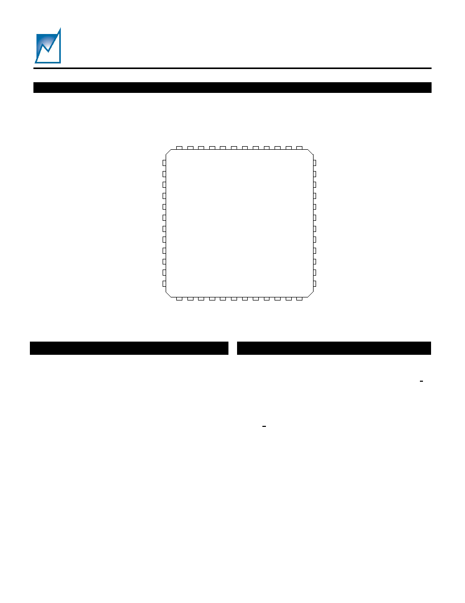
PACKAGE AND PIN CONFIGURATION
ABSOLUTE MAXIMUM RATINGS
RECOMMENDED OPERATING CONDITIONS
Temperature Under Bias ................. ≠55
∞
C to +125
∞
C
Storage Temperature ....................... ≠65
∞
C to +150
∞
C
Terminal Voltage with Respect to GND:
VI & VO Inputs ................................ ≠0.3V to 7.0V
VGATE, VGG_CAP
Outputs ........................... 16V
All Others ........................................ ≠0.3V to 7.0V
Output Short Circuit Current ............................. 100mA
Lead Solder Temperature (10 secs) .................. 300
∞
C
Junction Temperature ......................................... 150∞C
ESD Rating per JEDEC ..................................... 2000V
Latch-Up testing per JEDEC ..........................
± 100mA
Stresses listed under Absolute Maximum Ratings may cause
permanent damage to the device. These are stress ratings only and
functional operation of the device at these or any other conditions
outside those listed in the operational sections of the specification is
not implied. Exposure to any absolute maximum rating for extended
periods may affect device performance and reliability. Devices are
ESD sensitive. Handling precautions are recommended.
Temperature Range (Industrial).......... ≠40
∞
C to +85
∞
C
(Commercial) ........... ≠5
∞
C to +70
∞
C
Supply Voltage ..................................... 2.7V to 6.0V
1/
Package Thermal Resistance (
JA)
48 Lead TQFP ............................................ 80
o
C/W
Moisture Classification Level 1 (MSL 1) per J-STD- 020
Notes: 1/ For reliable operation the VDD_CAP node voltage must
be equal to or greater than 2.7V (voltage level measured
on pin 42).
RELIABILITY CHARACTERISTICS
Data Retention ............................................ 100 Years
Endurance .......................................... 100,000 Cycles
Note: Accuracy data is stored in pages 13-15 of the EEPROM
memory array. Erasure of this data will render the SMT4004A GUI
unusable. Loss of this data will not alter preset UV/OV trip points.
1
2
3
4
5
6
7
8
9
10
11
12
13
14
15
16
17
18
19
20
21
22
23
24
36
35
34
33
32
31
30
29
28
27
26
25
48
47
46
45
44
43
42
41
40
39
38
37
LDO#
W DO#
CROW BAR
1.25VREF
M R#
IRQ_CLR#
IRQ#
PGND
TRKR_IRQ#
SEATED1#
UV_OVERRIDE
SEATED2#
CB2
CB3
CB4
PW R_ON
VGATE1
VGATE2
VGATE3
VGATE4
VGG_CAP
FORCE_SD
CBFAULT
HEALTHY#
WL
D
I
SCL
SDA
A2
A1
A0
VD
D_
CA
P
VI
1
VI
2
VI
3
CB
1
VI
4
RST
1
#
RST
2
#
RS
T3
#
RST
4
#
PGND
DG
N
D
AG
N
D
VO1
VO2
VO3
EN
A
B
L
E
VO4
48 Lead TQFP

SMT4004A
Summit Microelectronics, Inc
2072 1.1 3/7/03
13
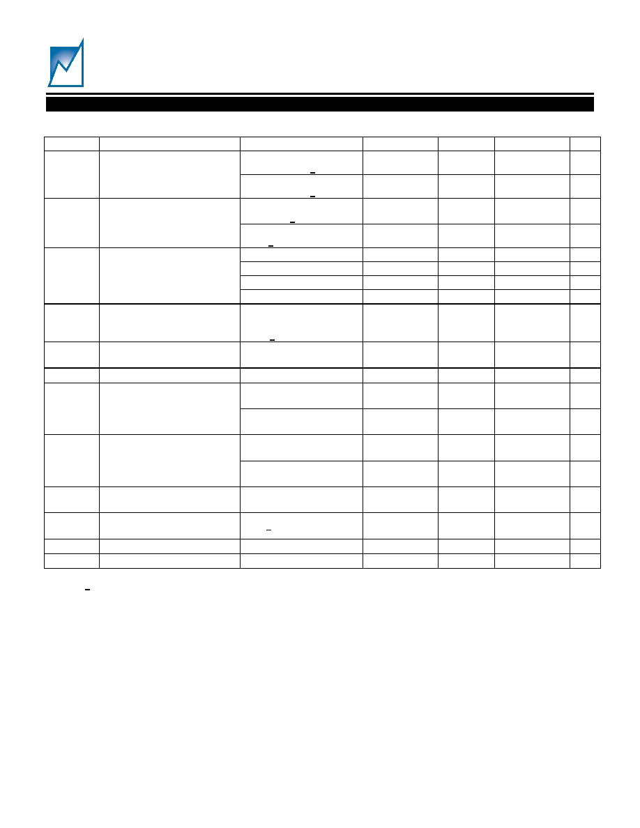
DC OPERATING CHARACTERISTICS
(Over recommended operating conditions, unless otherwise noted. All voltages are relative to GND.)
Symbol Parameter
Conditions
Min. Typ. Max Unit
V
SUPPLY
Power Supply Voltage
Device supply voltage
provided by the
highest VIX input.
2.7 6.0
V
VX
Monitoring Voltage
VI1-VI4, VO1-VO4
Note 1/
0
6.54
V
I
DD
Power Supply Current
VGATE Outputs
enabled, write to EE
memory array -
Note 2/
5 mA
PVIT
UV
Programmable VI
Threshold for UV condition
See explanation on
page 2
0.9 6.0
V
PVIT
OV
Programmable VI
Threshold for OV condition
See explanation on
page 2
1.08 6.6
V
PVIT
HYS
OV/UV trip hysteresis
10
mV
PVIT
UVACC
Programmable UV
Threshold Accuracy
Note 3/
0.99xPVIT
UV
PVIT
UV
1.01xPVIT
UV
V
PVIT
OVACC
Programmable OV
Threshold Accuracy
Note 3/
0.99xPVIT
OV
PVIT
OV
1.01xPVIT
OV
V
PVOT
UV1
Programmable VO
Threshold for UV1
condition
See explanation on
page 2
0.9 6.0
V
PVOT
UV2
Programmable VO
Threshold for UV2
condition
See explanation on
page 2
0.69xPVOT
UV1
PVOT
UV1
V
PVOT
UV1ACC
Programmable UV1
Threshold Accuracy
0.99xPVOT
UV1
PVOT
UV1
1.01xPVOT
UV1
V
PVOT
UV2ACC
Programmable UV2
Threshold Accuracy
0.95xPVOT
UV2
PVOT
UV2
1.05xPVOT
UV2
V
CB Trip Point = 25mV
19
25
31
mV
V
CB
Programmable circuit
breaker trip voltage
CB Trip Point = 50mV
37
50
62
mV
CB=25mV
QT=55mV
40 55 70
mV
CB=50mV
QT=80mV
60 80 100
mV
CB=25mV
QT=85mV
65 85 105
mV
CB=50mV
QT=110mV
80 110 140
mV
CB=25mV
QT=135mV
100 135 170
mV
V
QT
Programmable Quick Trip
Threshold Voltage
CB=50mV
QT=160mV
120 160 200
mV
Notes: 1/
VX is the entire operating range of the VIX and VOX input pins. Any of these inputs can be at ground potential.
2/
Does not include external load on VDD_CAP. Any external pull-up resistors tied to VDD_CAP will increase I
DD
. Maximum allowable
external current sourced from VDD_CAP is 1mA with VDD_CAP=10
µ
F.
3/
1% accuracy can be achieved for either bus-side UV or bus-side OV, but not both. This is due to the relationship between OV and
UV settings noted on page 2 of this data sheet. However, a 1% accuracy is achieved when monitoring bus-side OV and card-side
UV1. To obtain this accuracy, OV is set to the minimum setting (decimal value = 0) and adjusted with the UV setting to reach the
desired 1% OV trip point.
Accuracy data is stored in pages 13-15 of the EEPROM memory array. Erasure of this data will render
the SMT4004A GUI unusable. Loss of this data will not alter preset UV/OV trip points.
SMT4004A
Summit Microelectronics, Inc
2072 1.1 3/7/03
14
DC OPERATING CHARACTERISTICS
(CONTINUED)
(Over recommended operating conditions, unless otherwise noted. All voltages are relative to GND.)
Symbol Parameter
Conditions Min.
Typ.
Max
Unit
ON ( I
VGATE
= 4µA)
- Note 4/
12
16
V
V
VGATE
VGATE drive output
OFF (I
VGATE
= -8mA)
- Note 4/
0
0.4
V
All VGATEs forced to
10V
- Note 4/
10
µA
I
VGATE
Total VGATE output drive
current
All VGATEs forced to 1V
- Note 4/
30
µA
SR
VOX
= 100V/s 60
100
140
V/s
SR
VOX
= 250V/s
150 250 350
V/s
SR
VOX
= 500V/s
400 500 600
V/s
SR
VOX
Tracking VOX Slew Rate
SR
VOX
= 1000V/s 800
1000
1200
V/s
V
TRKR
Tracking Differential Voltage
Differential between
Tracking VOX pins
-
Note 5/
100
250
mV
V
TRKR_IRQ#
Tracking Differential Voltage
Causes TRKR_IRQ#
Differential between
Tracking VOX pins
300
mV
V
REF
1.25VREF Output Voltage
R
LOAD
= 2K
to gnd
1.23 1.25 1.27
V
VDD_CAP = 2.7V to
4.5V
0.9xVDD_CAP
6.0
V
V
IH
Input High Voltage
VDD_CAP = 4.5V to
6.0V
0.7xVDD_CAP
6.0
V
VDD_CAP = 2.7V to
4.5V
-0.1
0.1xVDD_CAP
V
V
IL
Input Low Voltage
VDD_CAP = 4.5V to
6.0V
-0.1
0.2xVDD_CAP
V
V
OL
Output Low Voltage
Open-drain Outputs, I
OL
= -2mA
0 0.4
V
V
CSWFZ
Card-Side Wait-For-Zero
Threshold
Note 6/
0.5 1.2
V
R
Pull-Up
Input Pull-Up Resistors
See Pin Descriptions
50
100
165
k
V
CROW
CROWBAR Output Voltage R
LOAD
=10k
to gnd
VDD_CAP-0.5
VDD_CAP
V
Notes: 4/
I
VGATE
is the sum of all VGATE output currents.
5/
The SMT4004A adjusts the VGATE outputs to control the differential of the VOX outputs to within 100mV nominally. External
influences may increase the differential until the VGATE outputs adjust to minimize the differential.
6/
Guaranteed by Design.
SMT4004A
Summit Microelectronics, Inc
2072 1.1 3/7/03
15
AC OPERATING CHARACTERISTICS
(Over recommended operating conditions, unless otherwise noted. All voltages are relative to GND.)
Symbol Description
Conditions Min.
Typ.
Max.
Unit
CB
DELAY
= 25µs
20
25
40
µs
CB
DELAY
= 50µs
40
50
80
µs
CB
DELAY
= 100µs
80
100
140
µs
CB
DELAY
Programmable Circuit Breaker Filter
CB
DELAY
= 200µs
160
200
280
µs
t
PWDTO
= 400ms
t
PWDTO
= 800ms
t
PWDTO
= 1600ms
t
PWDTO
Programmable Watchdog Timer
Time-Out Period
t
PWDTO
= 3200ms
-25 t
PWDTO
+25 %
t
PLDTO
= 800ms
t
PLDTO
= 1600ms
t
PLDTO
= 3200ms
t
PLDTO
Programmable Longdog Timer Time-
Out Period
t
PLDTO
= 6400ms
-25 t
PLDTO
+25 %
t
PRTO
= 25ms
t
PRTO
= 50ms
t
PRTO
= 100ms
t
PRTO
Programmable Reset Time-Out
Period
t
PRTO
= 200ms
-25 t
PRTO
+25 %
t
CROW
CROWBAR output pulse width
SCR Mode, R
LOAD
=10k
6 10
15
µs
t
DFIRQ
Delay from fault detection to IRQ#
1
µs
t
DFRST
Delay from fault detection to RST#
1
µs
t
DFHEALTHY#
Delay from fault detection to
HEALTHY#
1
µs
t
DTKRIRQ
Delay from tracking fault detection to
TRKR_IRQ#
1
µs
t
DFCR
Delay from fault detection to
CROWBAR
1
µs
t
DMRRST
Delay from assertion of MR# to
RST# Active
100
ns
t
DVIVG
Delay from VIX valid to VGATEX
activated
VGG_CAP=14V 0
µs
t
DFSVG
Delay from assertion of FORCE_SD
to VGATE clamped to ground.
10
µs
SMT4004A
Summit Microelectronics, Inc
2072 1.1 3/7/03
16
I
2
C 2-WIRE SERIAL INTERFACE AC OPERATING
CHARACTERISTICS - 100kHz
(Over recommended operating conditions, unless otherwise noted. All voltages are relative to GND.)
Symbol Description
Conditions
Min
Typ
Max
Units
f
SCL
SCL Clock Frequency
0 100
KHz
t
LOW
Clock Low Period
4.7 µs
t
HIGH
Clock
High
Period
4.0 µs
t
BUF
Bus Free Time
Before New Transmission
Note 1/
4.7 µs
t
SU:STA
Start Condition Setup Time
4.7
µs
t
HD:STA
Start Condition Hold Time
4.0
µs
t
SU:STO
Stop Condition Setup Time
4.7
µs
t
AA
Clock Edge to Data Valid
SCL low to valid SDA (cycle n)
0.2
3.5
µs
t
DH
Data Output Hold Time
SCL low (cycle n+1) to SDA
change
0.2 µs
t
R
SCL and SDA Rise Time
Note 1/
1000
ns
t
F
SCL and SDA Fall Time
Note 1/
300
ns
t
SU:DAT
Data In Setup Time
250
ns
t
HD:DAT
Data In Hold Time
0
ns
TI
Noise Filter SCL and SDA
Noise suppression
100
ns
t
WR
Write
Cycle
Time
5
ms
Note: 1/ - Guaranteed by Design.
TIMING DIAGRAMS
t
R
t
F
t
HIGH
t
LOW
t
SU:SDA
t
HD:SDA
t
SU:DAT
t
HD:DAT
t
SU:STO
t
BUF
t
DH
t
AA
SCL
SDA
(IN)
SDA
(OUT)
t
W R (For W rite Operation Only)
Figure 8 . Basic I
2
C Serial Interface Timing
SMT4004A
Summit Microelectronics, Inc
2072 1.1 3/7/03
17
Soft Start
VGATEs
ENABLE
PW R_ON
SEATED1&2#
Tracking
VGATEs
FORCE_SD
Figure 9. De-asserting the VGATE Outputs with the Enabling Inputs
Composite
RST#
MR#
WDO#
LDO#
WLDI
t
0
t
0
t
0
t
0
t
PW DTO
t
PW DTO
t
PLDTO
t
0
<t
PWDTO
t
PLDTO
t
PRTO
t
PLDTO
t
0
t
PWDTO
t
PRTO
t
0
<t
PLDTO
t
PRTO
Figure 10. Relation of LDO# and WDO# with WLDI, RST# and MR#
TIMING DIAGRAMS
(CONTINUED)
SMT4004A
Summit Microelectronics, Inc
2072 1.1 3/7/03
18
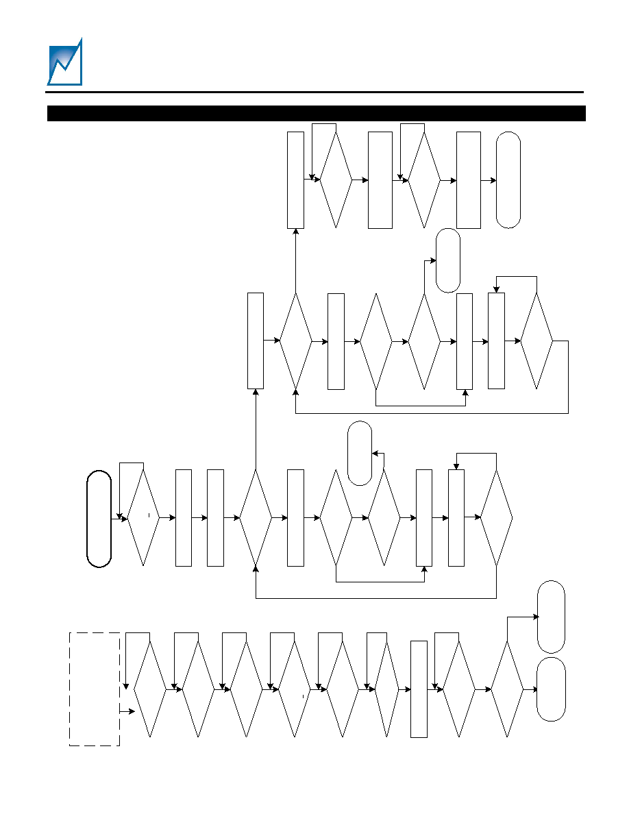
APPLICATIONS INFORMATION
A
PPLICATIONS EXAMPLE
The timing diagram in Figure 11 illustrates a full power-on and power-off sequence and the relationship between
many of the signals. This is based on the simplified applications diagram on Page 1. Manager 1 is programmed to
softstart. Its supply feeds two power supplies that are monitored by managers 3 and 4 that, along with manager 2,
are programmed for tracking. The flow chart in Figures 12A and 12B are a further illustration of the same application.
VI1
VGATE1
VO1
VI2
VI3
VI4
P
VIT
1
P
VIT
2
P
VIT
3
P
VIT
4
P
VOT
1
P
VOT
2
P
VOT
3
P
VOT
4
VO2
VO3
VO4
Composite
VO2,3 & 4
VGATE2
VGATE3
VGATE4
VO2
VO3
VO4
=
+
+
RST#s
t
PRTO
HEALTHY#
PW R_ON
ENABLE
Figure 11 ≠ Timing of Events During Power-On and Power-Off sequences.
SMT4004A
Summit Microelectronics, Inc
2072 1.1 3/7/03
19
APPLICATIONS INFORMATION
(CONTINUED)
YES
C
O
M
P
AR
E VO
I
N
PU
T
S
YES
NO
NO
NO
YE
S
YES
T
R
A
CKI
NG RO
U
T
I
N
E
VI
4
>
PVI
T
OV
4?
NO
YE
S
A
D
J
U
ST
VG
AT
E
O
U
T
P
U
T
S
R
E
M
O
VE
V
O
4
F
R
O
M
T
R
AC
K
I
NG
> 10
0m
V
?
> 30
0m
V
?
A
D
J
U
ST
VG
AT
E
O
U
T
P
U
T
S
C
O
M
P
AR
E
VO
I
N
PU
T
S
> 10
0m
V
?
C
O
M
P
AR
E VO
I
N
P
U
T
S
YE
S
NO
NO
YE
S
YES
V
I
3
>
PVI
T
OV
3?
NO
>
100
m
V
?
>
3
0
0m
V
?
AD
J
U
S
T
VG
A
T
E
O
U
T
P
U
T
S
C
O
M
P
AR
E VO
I
N
PU
T
S
>
10
0m
V
?
R
E
MO
V
E
VO
3
F
R
O
M
T
R
A
C
KI
NG
V
I
2
>
PVI
T
OV
2?
NO
YE
S
YES
ST
AR
T
R
E
SET
T
I
M
E
R
A
S
S
E
R
T
HE
A
L
T
H
Y
#
OUT
P
UT
RE
S
E
T
T
I
M
E
D O
U
T
?
S
T
A
R
T LONGDO
G
S
T
A
R
T WA
TC
H
D
O
G
GO
TO
GE
N
E
R
A
L
MONI
T
O
R
ROUT
I
N
E
NO
YE
S
GO
TO
S
H
U
T
D
O
W
N
RO
U
T
I
N
E
YES
NO
G
O
T
O
S
H
UT
DO
W
N
RO
UT
I
N
E
NO
YE
S
VI
2
,
VI
3
,
VI
4
PVI
T
UV
1
&
VI
2
,
V
I
3
,
VI
4
<
PVI
T
OV
1
?
T
U
R
N
ON
V
G
A
T
E
OU
T
P
U
T
S
YE
S
T
u
r
n
O
N
VG
AT
E1
PW
R
_
O
N
T
R
UE?
EN
AB
L
E
A
S
SE
R
T
E
D
?
FO
R
C
E_
SD
FA
L
S
E
?
VI
1
PVI
T
UV
1
&
V
I
1
<
PVI
T
OV
1
?
CB
1
O
K
?
VI
1
PVI
T
OV
1
?
NO
YE
S
NO
YES
NO
YES
NO
YES
NO
YES
NO
SEAT
E
D
1
#
and
S
E
A
T
E
D2#
T
RUE?
NO
YES
YE
S
G
O
T
O
T
R
A
C
KI
NG
RO
UT
I
N
E
GO
T
O
S
HUT
DOW
N
ROU
T
I
N
E
M
a
na
ge
r
1
= S
o
f
t
s
t
a
r
t
M
a
na
ger
s
2
,
3
and 4
=
Tr
ack
i
n
g
VI
2
>
VI
3
>
VI
4
I
S
VG
G
Vo
l
t
age
F
u
l
l
y
O
N
?
NO
YES
YES
Figure 12A ≠ Power-On Sequence of Events
SMT4004A
Summit Microelectronics, Inc
2072 1.1 3/7/03
20
YES
ALL VOLTAGES WITHIN LIMITS?
VO4 <PVOT4?
ADJUST VGATE4
GENERAL MONITORING
OPERATION
NO
GO TO SHUTDOWN
ROUTINE
ALL CONTROL INPUTS VALID?
YES
NO
DID SEATED# GO HIGH?
YES
WAS ENABLE DEASSERTED?
YES
NO
NO
WAS PWR_ON DEASSERTED?
YES
YES
NO
ENABLE REMOVED ROUTINE
PWR_ON REMOVED ROUTINE
SEATED# REMOVED ROUTINE
GO TO PWR_ON
REMOVED ROUTINE
NO
GO TO ENABLE
REMOVED ROUTINE
GO TO SEATED#
REMOVED ROUTINE
DE-ASSERT HEALTHY#
ASSERT ENABLED RST#S
VO4 = VO3?
ADJUST VGATE4
NO
VO4&VO3 = VO2?
ADJUST VGATE4 & VGATE3
NO
YES
YES
VO4&VO3&VO2 = 0V?
ADJUST VGATE4, VGATE3 &
VGATE2
NO
YES
IS ENABLE DEASSERTED?
YES
GO TO ENABLE
REMOVED ROUTINE
NO
SHUTDOWN ALL ACTIVE VGATE
OUTPUTS
IF ON DE-ASSERT HEALTHY# &
IF OFF ASSERT ALL RST#
OUTPUTS
SHUTDOWN ALL ACTIVE VGATE
OUTPUTS
IF ON DE-ASSERT HEALTHY# &
IF OFF ASSERT ALL RST#
OUTPUTS
SHUTDOWN ROUTINE
SHUTDOWN ALL ACTIVE VGATE
OUTPUTS
IF ON DE-ASSERT HEALTHY# &
IF OFF ASSERT ALL RST#
OUTPUTS
IS VOX HIGH?
YES
NO
Figure 12B ≠ Power-Off Sequence of Events
APPLICATIONS INFORMATION
(CONTINUED)
SMT4004A
Summit Microelectronics, Inc
2072 1.1 3/7/03
21
SOFTSTART VS TRACKING
As a power supply manager the SMT4004A separates
two power domains; the bus-side, or source power
supplies, and the card-side that contains the
application circuitry. Its primary tasks are to monitor
the voltages and control the switching of the bus-side
voltages to the card-side circuits. The switching is
accomplished by providing a high-side drive output on
the VGATE pins. The VGATE output is applied to the
gates of the power MOSFET.
Softstart
The supply managers can act as either tracking
managers or as softstart managers. Individual
managers turn on their VGATE outputs once all
enabling conditions for that class of manager (softstart
or tracking) are met. If a manager is set to soft start,
its VGATE output ramps at a programmable constant
slew rate until it reaches its maximum value. This
operation is commonly used when a voltage (e.g., 5V)
is first switched into a DC-to-DC converter or group of
LDOs. These outputs may then be tracked to the
card-side logic.
Tracking
When a manager is programmed for tracking all
enabling conditions for that class of manager
(tracking) must be met before the VGATE outputs are
turned on. The enabling conditions also include all
softstart managers having their VGATE outputs fully
on with no existing fault conditions for the softstart
managers.
During tracking the card-side voltages are monitored
to minimize the differential voltage between each
tracked voltage until they reach their respective
undervoltage thresholds (UV1). In tracking mode the
ramp rates are constant but can stop and wait. That
is, if, during the tracking interval, there is any
difference between the VO inputs, the VGATE outputs
will stop and wait for the slow channel to catch up.
POWER-ON
Initial Conditions
At least one of the VI pins must be equal to or greater
than 2.85V before the power-on operation can
proceed. For reliable operation the VDD_CAP node
voltage must be equal to or greater than 2.7V (voltage
level measured on pin 42). This requires that at least
one of the VI inputs needs to be at or above 2.85V for
proper device operation. There is internal arbitration
circuitry which chooses the highest VIx to power the
SMT4004A and causes an internal voltage drop from
VIx to VDD_CAP.
Both SEATED# inputs must be low. The SEATED#
inputs are generally used with staggered-pin
applications where the connector for the application
card has two or three levels of pin lengths. This allows
`early-power' to be applied to the SMT4004A so it can
begin to monitor bus side supplies as they come up,
and also a method to indicate the application board is
fully seated and ready for operation. Removal of a
powered board is first recognized by the SEATED#
pins going high, causing power-off of the board by
shutting down the charge-pump, not ensuring a track
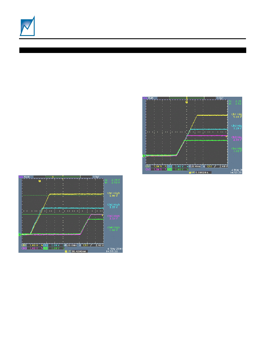
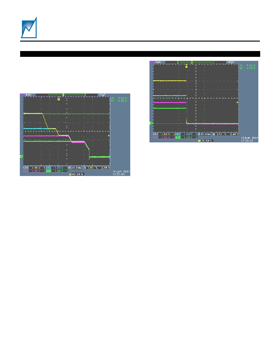
Scope Shot 1. Typical softstart Power-On by
twomanagers and tracking by two managers.
Scope Shot 2. Power-On with all four managers
set to track
.
APPLICATIONS INFORMATION
(CONTINUED)
SMT4004A
Summit Microelectronics, Inc
2072 1.1 3/7/03
22
down. In this application the SEATED# pins are
routed to the board's short pins and grounded when
the board is fully inserted. The SEATED# pins can be
tied to card insertion switches or they actively driven
and used as device enable inputs.
FORCE_SD can be programmed as a true high or true
low input. When asserted, the VGATE outputs are
turned off and clamped to ground. This input must be
false for power-on to proceed. This pin is internally
pulled up to the VDD_CAP node with a 100K
resistor.
The PWR_ON input can be programmed as a true
high or true low input. It must be true for both soft
start and tracking managers to turn on their VGATE
outputs. If the SMT4004A has already activated the
VGATE outputs and PWR_ON is turned off, only the
VGATE outputs for the tracking managers are turned
off. VGATE outputs programmed for soft start remain
active.
An I
2
C power-on function is available. This allows the
tracking power-on/off operations to be initiated by the
2-wire serial interface.
If the SMT4004A is configured for I
2
C power-on then
the PWR_ON pin must be in its true state.
The ENABLE input can be programmed to a true high
or true low input. The ENABLE input activates the
high-side driver charge pump and must be true for the
VGATE outputs to be able to drive the gates of the
external MOSFETs.
Managers programmed for soft start enable their
VGATE outputs once all softstarted VI inputs are
within their programmed threshold limits (UV and OV)
(Figure 13). Managers programmed for tracking
enable their VGATE output once softstarting is
successful and all tracking manager's VI inputs are
within their programmed threshold limits (Figure 14).
POWER-ON OPTIONS
Bus-side Over-voltage
If OV detection is selected and is programmed to be a
trigger source for IRQ#, and if IRQ# is a trigger source
for force shutdown (FSD), the user has several options
as to how the part reacts to an OV. Different options
can be chosen for how the SMT4004A will respond
during the time periods during power-on, after power-
on has completed, or when normal monitoring is
underway. OV detection must not be enabled on
disabled manager channels.
If an OV occurs after softstart has completed and
before tracking has begun, the SMT4004A can be
programmed to ignore the OV. A case where this
would be selected might be as illustrated in the
Simplified Applications drawing on Page 1. Assume
the +5V softstarts as planned and the LDO's are
energized. The LDOs might cause a temporary OV
condition before full regulation on the 1.5V or 2.5V
supplies occurs.
If the ignore option is selected the following are true:
1. Only managers with OV detection are
affected.
2. If OV occurs during softstart, the VGATE
outputs are turned off and remain off until the
OV condition is cleared.
3. If tracking has started and OV is detected, a
FORCE_SD is initiated.
APPLICATIONS INFORMATION
(CONTINUED)
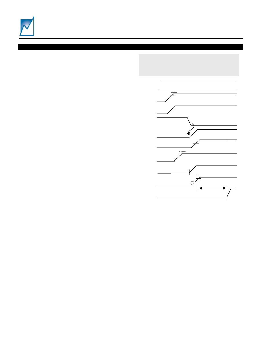
Assumptions: m anagers 1 & 2 are softstart, m anagers 3 & 4
are tracking and are not shown; Staggered pin application;
ENABLE true low and FORCE_SD true high, both tied to
ground; PW R_ON active high, tied to +5V thru pull up; only
RST1# and RST2# enabled.
FORCE_SD
VI1
PW R_ON
SEATED1&2#
VGATE1
VO1
VI2
VGATE2
VO2
VI1
UV
RST1# & RST2#
t
PRTO
VI1
OV
VO1
UV2
VO1
UV1
VI2
UV
VI2
OV
VO2
UV2
VO2
UV1
GND
GND
ENABLE
Figure 13. Typical Soft Start Sequence
SMT4004A
Summit Microelectronics, Inc
2072 1.1 3/7/03
23
Card-side Voltage
When tracking is selected the SMT4004A monitors the
VO inputs prior to initiating the tracking function. The
SMT4004A will not start tracking until the VO inputs
are below 0.5V (V
CSWFZ
). However, some systems may
partially charge one or more of the power busses if a
softstart voltage has energized some of the application
circuitry. If the charge is excessive (>V
CSWFZ
), tracking
will not start. The SMT4004A has two options that can
be selected to accommodate this situation.
1. The "Don't-Wait-For-Zero" (DWFZ) option can be
enabled. As the name implies the SMT4004A will
not monitor the VO inputs and tracking starts once
all UV, OV and enabling inputs are valid.
NOTE: If the starting VO potentials are too high,
tracking of low voltage supplies may not meet
some system specifications.
2. The CROWBAR pin is normally configured to
output a short positive pulse to trigger an SCR.
Optionally it can be configured as a normally
active high output during the power-on phase prior
to tracking. Configured as such, it can be used to
drive the gate of an N-channel MOSFET to
actively discharge any `early voltages.' Once
tracking is initiated, the CROWBAR output goes
low allowing the card-side voltages to turn-on.
Refer to Figure 15 for a schematic illustration.
NOTE: This feature can be used independently or
in conjunction with the DWFZ option.
Tracking Failure Options
During tracking differentials greater than 300mV
between VO inputs can be reported through the
assertion of the TRKR_IRQ# output. Any tracking
manager detecting a failure can generate an interrupt,
and any tracking manager can be assigned to track
but not generate an interrupt.
If a manager is assigned to track, and a tracking error
is detected, the SMT4004A can be programmed to
take one of the following actions.
∑ Ignore the condition and proceed with the
power-on operation.
∑ Shutdown all supplies and generate a
TRKR_IRQ#.
∑ Generate a TRKR_IRQ# and proceed with the
power-on operation.
R
G1
10
VI
1
CB
1
VG
A
T
E1
VO
1
Q1
VOUT
to Application
Circuit
R
S
PG
N
D
PGN
D
CROW BAR
VIN
Common
GND
SM T4004A
C
G1
10nF
Figure 15 - Example implementation of the `Early
Drive Function.'
APPLICATIONS INFORMATION
(CONTINUED)
Assumptions: m anagers 1 and 2 are tracking managers;
Managers 3 & 4 are turned off; FORCE_SD is active high
and ENABLE is active low, both tied to ground; PW R_ON is
active high tied to VDD thru a pull-up resistor; the SEATED#
inputs are tied to ground.
VI1
PW R_ON
SEATED1&2#
VGATE1
VO1
VI2
VGATE2
VO2
VI1
UV
RST1# & RST2#
t
PRTO
VI1
OV
VO1
UV2
VO1
UV1
VI2
UV
VI2
OV
VO2
UV2
VO2
UV1
gnd
VO1
UV1
Composite VO1
and VO2
VO1
VO2
FORCE_SD
GND
GND
ENABLE
Figure 14 - Typical tracking sequence of operation.
SMT4004A
Summit Microelectronics, Inc
2072 1.1 3/7/03
24
POWER-OFF
Power-off of the application circuit is affected by
turning off the VGATE outputs. This can be done by
de-asserting one of the enabling signals or the
detection of a fault condition. When the SMT4004A
receives a power-off command, whether it is from the
PWR_ON pin, an I
2
C command, or from the latching of
a fault, there will be a delay of approximately
VI
MAX
/Tracking Slew Rate (where VI
MAX
is the VI with
the highest voltage level) before the first tracked
VGATE begins to discharge.
Enabling Inputs
If the PWR_ON input is de-asserted tracking
managers will `track down' their voltages. The
softstart managers are unaffected and their VGATE
outputs remain active. If either or both SEATED#
inputs are de-asserted the SMT4004A immediately
powers-off the VGATE outputs.
If the FORCE_SD input is asserted the managers
immediately shut off the VGATE drivers by clamping
these outputs to ground (Scope Shot 4).
If the ENABLE input is de-asserted, the VGATE
outputs are shut off. Refer to Figure 9 for an
illustration of de-asserting the various enabling inputs.
SOFTWARE POWER-ON/POWER-OFF
The SMT4004A has an option allowing a commanded
power-on and power-off via the I
2
C serial interface of
tracked channels. If the device is configured for this
option, the PWR_ON pin must be in the true state.
Once all enabling conditions are met and all voltages
are within their thresholds the SMT4004A can be
tracked-up by writing to register 16. Once the
application circuit is tracked-up a subsequent write to
register 17 initiates a track down. Refer to the
applications circuits and descriptions for a system
level description.
RESET OPERATION
Once power is applied to the SMT4004A the four
RST# outputs are driven low. Because they are
meant to be used by the application circuitry, the
RST# outputs remain low until all Reset trigger
sources (for any manager's UV1, UV2 or QT-CB
output) are removed. The RST# outputs remain low
for the duration of the programmable reset time-out
period (t
PRTO
) after the triggers are cleared.
After the circuitry is `powered-on' and the SMT4004A
is in the steady-state monitoring mode, the RST#
outputs remain high unless one of the enabled fault
conditions is detected by a manager. When this
occurs only the RST# output affected by that manager
is asserted. All RST# outputs that have gone low to
indicate a problem on their corresponding channel will
remain low until all reset conditions have been
removed and t
PRTO
has expired.
Scope Shot 3. Power-Off caused by de-assertion of
PWR_ON ( all managers selected for tracking).
Scope Shot 4. Power-Off of all managers using
the FORCE_SD pin.
APPLICATIONS INFORMATION
(CONTINUED)

SMT4004A
Summit Microelectronics, Inc
2072 1.1 3/7/03
25
All four RST# outputs are driven low when the MR#
input is taken low. They continue to assert their
outputs after MR# returns high for t
PRTO
seconds.
INTERRUPTS, FORCE SHUTDOWN AND
CROWBAR
The SMT4004A has two interrupt outputs: IRQ# and
TRKR_IRQ#. The CROWBAR output is configurable
to operate in conjunction with the IRQ# outputs.
The IRQ# output has a large number of programmable
sources for latching its output. Any combination of
supply manager fault condition outputs (UV, OV, UV1,
UV2 and QT-CB) can be enabled as a trigger for the
IRQ# latched output. Once triggered the IRQ# output
is latched and remains asserted even if the fault
condition is removed. IRQ# can only be cleared by
asserting the IRQ_CLR# input.
IRQ# can also trigger a force shutdown (FSD) and/or a
CROWBAR pulse. Refer to Figure 3 and the graphical
user interface (GUI) for the SMT4004A.
During the power on sequence of the SMT4004A the
IRQ# output is disabled for the IRQ# hold-off time
period. This time period begins when the PWR_EN
and ENABLE are active. Once the IRQ# hold-off time
period expires any programmed IRQ condition will
trigger the IRQ# output. The IRQ# hold-off time period
precedes the Reset timeout period. If the reset
conditions are removed before the end of the IRQ#
hold-off time period the reset timeout period will begin
after the IRQ# hold-off timer has timed out.
The hold
off can be extended from the end of the Reset timeout
period for 0ms, 200ms, 400ms, 800ms or 1600ms.
This allows the application circuit and all of the
supplies time to stabilize after the initial power-on.
The VGATE control circuitry monitors VO inputs for
those managers selected for tracking. If a VO input is
found to not be tracking, or deviates from the other
voltages by more than 300mV, the control circuitry
generates a tracker error. If that output is ANDed with
an enable bit it forces the TRKR_IRQ# output low. No
other fault conditions can generate a TRKR_IRQ#.
TRKR_IRQ# can trigger an internal force shutdown
and/or a CROWBAR pulse like the IRQ# output.
If the fault latch feature is enabled the fault condition is
captured. The fault sources are a forced shutdown,
CROWBAR, or IRQ#. When a fault is detected a
volatile latch is set to keep the SMT4004A from being
powered-up again until IRQ_CLR# is toggled.
The CROWBAR pin is designed to deliver an active
high pulse to an external SCR to shutdown the card-
side voltages as quickly as possible. A CROWBAR
pulse can be triggered by one of seven inputs: a QT-
CB fault, an IRQ#, a TRKR_IRQ# and/or assertion of
the FORCE_SD input. These trigger sources are
optional and any combination can be selected. Note:
because an over-current condition is potentially
catastrophic, each manager has a unique source input
to the CROWBAR logic even though they are included
in the trigger sources for an IRQ#. This allows less
harmful fault triggers to be used as inputs for the IRQ#
without generating a CROWBAR. There is also an
option to change the CROWBAR pin output from an
SCR pulse to a voltage level to discharge Card-side
early voltages prior to tracking (see Figure 15).
WATCHDOG AND LONGDOG TIMERS
The SMT4004A has two timers that generate
independent outputs: the WDO#, or watchdog timer
output, and the LDO#, or longdog timer output. Both
timers use the same clock circuitry. However, the time
out period for each timers is independently
programmable. When the timer has timed out for
either the watchdog or the longdog, their respective
outputs are driven low. The timers are Reset to t
0
by a
low-to-high transition on the WLDI input.
Note: If WLDI is held high the WDO# output is
disabled and the LDO# transitions low after its
programmed time out period t
PLDTO
. It remains low for
t
PLDTO
returning high for t
PLDTO
seconds, and repeating
the pulse output until the next low-to-high transition on
the WLDI input.
Both timers are disabled during the initial power-on
operation and will not start until all RST# outputs have
been released. The end of the initial programmable
reset time-out period, t
PRTO,
is effectively t
0
for both
timers. Asserting MR# or the occurrence of a fault
condition causing any Reset disables the timers until
the RST# outputs are released. Refer to Figure 10 for
an illustration of the relation between the timer
outputs, WLDI and the Reset functions.
SERIAL INTERFACE
Access to the configuration registers and memory
array is carried out over an industry standard 2-wire
serial interface (I
2
C). SDA is a bi-directional data line
and SCL is the clock input. Data is clocked in on the
rising edge of SCL and clocked out by the falling edge
of SCL. All data transfers begin with the MSB. During
data transfers SDA must remain stable while SCL is
APPLICATIONS INFORMATION
(CONTINUED)

SMT4004A
Summit Microelectronics, Inc
2072 1.1 3/7/03
26
high. Data are transferred in 8-bit packets with an
intervening clock period in which an acknowledge is
provided by the device receiving data.
The SCL high period (t
HIGH
) is used for generating start
and stop conditions that precede and end most
transactions on the serial bus. A high-to-low transition
of SDA during t
HIGH
is a start condition and a low-to-
high transition of SDA during t
HIGH
is a stop condition.
The interface protocol allows operation of multiple
devices and types of devices on a single bus through
the use of unique device addressing. The address
byte is comprised of a 4-bit device type identifier, a 3-
bit bus address, and a single bit indicating that the
operation is a read or a write. Refer to Table 2 for an
illustration of the configuration of the address as
defined for the SMT4004A.
The device type identifier for the memory array is
generally set to 1010
BIN
following the industry standard
for a typical nonvolatile memory. There is an option to
change the identifier to 1011
BIN
allowing it to be used
on a bus that may be occupied by other memory
devices. The configuration and fault status registers
are accessible with a separate device type identifier of
1001
BIN
.
The bus address is defined by the state (`0' or `1') of
the A0, A1 and A2 pins. The serial data stream must
match the state of these pins.
WRITE
Writing to the memory or a configuration register is
illustrated in Figures 16 and 18. A start condition
followed by the address byte is provided by the host;
the SMT4004A responds with an acknowledge; the
host then responds by sending the memory address
pointer or configuration register address pointer; the
SMT4004A responds with an acknowledge; the host
then clocks in the data. For memory writes an
additional 15 bytes of data can be written. Only one
configuration register can be written per data transfer.
After the last byte is clocked in a stop condition must
be issued for the nonvolatile write operation to
proceed.
READ
The address pointer for the registers and the memory
can only be changed by a write command. If a read
command is issued without address conditioning the
data that is clocked out will be from a location pointed
to by the last written (or read) address incremented by
one.
In order to read data from a specific location a false
write command is issued. The sequence is: issue a
start and a device address with a write command; wait
for an acknowledge; send the array or register
address; wait for an acknowledge; issue a new start
and device address with a read command; wait for an
acknowledge then proceed to clock out data. For
memory reads the host can acknowledge receipt of
data and then continue clocking out data and
acknowledging without restriction. For register reads
only a single location can be read with each command
sequence. All read operations are concluded by
issuing a stop condition. Refer to Figures 17 and 19
for an illustration of the read sequence.
MR# AND THE SERIAL INTERFACE
When writing the memory array the MR# input must be
high. When writing the memory array the SMT4004A
cannot be in reset.
When reading the status registers or memory array the
state of the MR# input is ignored.
When writing the configuration registers the default
requirement for MR# is for it to be asserted or low.
There is an option that allows this to be a `don't care'
input; that is, the pin can be high or low and the
configuration registers can be written. [This option is
chosen on the Miscellaneous Settings tab of the
Windows GUI]
Table 2. Address Bytes
Device Identifier
Bus Address
R/W
D7 D6 D5 D4 D3 D2 D1 D0
Action
1 0 1 0 A2
A1
A0 1
Read
Memory
1 0 1 0 A2
A1
A0 0
Write
Memory
1 0 1 1 A2
A1
A0 1
Read
Memory
(alternate
address)
1 0 1 1 A2
A1
A0 0
Write
Memory
(alternate
address)
1 0 0 1 A2
A1
A0 1
Read
Registers
1 0 0 1 A2
A1
A0 0
Write
Registers
APPLICATIONS INFORMATION
(CONTINUED)
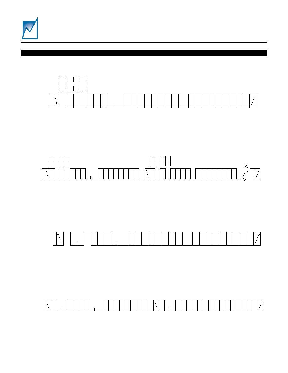
SMT4004A
Summit Microelectronics, Inc
2072 1.1 3/7/03
27
1
0
0
1
A
2
A
1
A
0
W
A
C
K
A
2
A
1
A
0
D
2
D
1
D
0
D
5
D
4
D
3
D
7
D
6
A
7
A
6
A
5
A
4
A
3
SDA
A
C
K
A
C
K
S
T
O
P
S
T
A
R
T
M aster
SM T4004
1
0
1
1
Optional Device
Type Identifier
Bus Address =
Address Pins
Memory Address Location
Figure 16. Memory Write Sequence.
A
C
K
A
2
A
1
A
0
D
2
D
1
D
0
D
5
D
4
D
3
D
7
D
6
A
7
A
6
A
5
A
4
A
3
SDA
A
C
K
A
C
K
S
T
O
P
S
T
A
R
T
M aster
SM T4004
1
0
0
1
A
2
A
1
A
0
W
1
0
0
1
A
2
A
1
A
0
R
S
T
A
R
T
A
C
K
N
A
C
K
1
0
1
1
Optional Device
Type Identifier
1
0
1
1
Optional Device
Type Identifier
Bus Address =
Address Pins
Memory Address Location
Figure 17. Memory Read Sequence.
1
0
0
1
A
2
A
1
A
0
W
A
C
K
C
2
C
1
C
0
D
2
D
1
D
0
D
5
D
4
D
3
D
7
D
6
X
X
X
C
4
C
3
SDA
A
C
K
A
C
K
S
T
O
P
S
T
A
R
T
M aster
SM T4004
Bus Address =
Address Pins
Configuration
Register
Address
Figure 18. Write Configuration Register Sequence.
A
C
K
C
2
C
1
C
0
D
2
D
1
D
0
D
5
D
4
D
3
D
7
D
6
SDA
A
C
K
N
A
C
K
S
T
O
P
S
T
A
R
T
M aster
SM T4004
1
0
0
1
A
2
A
1
A
0
W
1
0
0
1
A
2
A
1
A
0
R
S
T
A
R
T
A
C
K
Bus Address =
Address Pins
Configuration
Register
Address
Bus Address =
Address Pins
X
X
X
C
4
C
3
Figure 19. Read Configuration Register or Status Register Sequence.
APPLICATIONS INFORMATION
(CONTINUED)

SMT4004A
Summit Microelectronics, Inc
2072 1.1 3/7/03
28
PROTOTYPING WITH THE SMT4004A WINDOWS
GUI SOFTWARE
For prototyping and device evaluation use the
Windows Graphical User Interface (GUI) and
SMX3200 device programmer with the SMT4004A.
The programming system is available from the Summit
website (
www.summitmicro.com
). Further explanation
of the 32 individual configuration registers and
associated GUI settings are included in Application
Note 22.
After installing and starting the interface the screen will
display six different tabs. (Before proceeding, click on
the Read Config button or Load Defaults). Each tab
represents a group of functions and features that need
to be selected for the end application.
Power Managers, Resets and IRQ#s TAB
This screen allows the user to select any one of the
four managers and then configure its operation. The
required information for each manager is:
Enable or disable the manager. If a manager is
disabled, OV must be disabled on that manager.
Tracking Mode or Soft Start.
Bus-Side Operation: adjust the UV and OV
thresholds enable their use individually.
Card-Side Operation: adjust the UV1 and UV2
thresholds and enable the use of UV2.
Turn off or select a QT threshold.
Select the sources that can trigger an interrupt.
Select the sources that can trigger a Reset.
Slew Rate, Timer and Circuit Breaker
Select the VGATE slew rate for both power-on and
power-off.
The Circuit breaker delay is the programmable
filter.
The 300mV Trakker Action refers to the optional
actions that can be taken if a differential of more
than 300mV is detected by tracking managers.
Select which manager can generate a
TRKR_IRQ#.
Select the reset timeout period.
Select both the LDO# and WDO# timer values.
Crowbar and Pin Polarity
Select one or more Crowbar Source Enables.
Select Crowbar pin function.
Select "Active" pin polarity.
IRQ#, Circuit Breaker, OV Settings
These are important house keeping chores that need
to be selected.
Starting at the bottom:
Configure the IRQ# options.
Next:
The circuit breaker trip point is the voltage drop
across the sense resistor that will be used to
determine an over-current condition.
The last two boxes determine the action that is
taken if an over-current condition exists.
Miscellaneous Settings
MRB (MR#), I
2
C power-On/Off Memory Address
Select and Bus Address Response all configure
the operation of the serial interface.
Select Fault Latching Capability.
Select whether the VO inputs need to be near 0V
before tracking commences (Disable option).
Memory Array and Status Regs
The memory array function allows reading and writing
the array. The GUI screen displays an `address-
relative' bit map of the contents of the array.
This TAB provides access to the fault status registers
and the ability to clear them during debug.
APPLICATIONS INFORMATION
(CONTINUED)
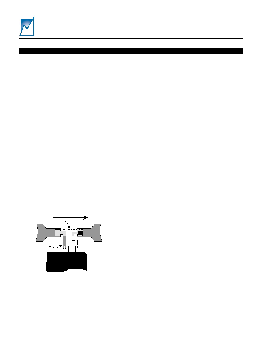
SMT4004A
Summit Microelectronics, Inc
2072 1.1 3/7/03
29
APPLICATIONS INFORMATION
(CONTINUED)
USE A KELVIN CONNECTION FOR ACCURATE
CURRENT MEASUREMENT
High current measurements using a series resistor can
be very accurate when a Kelvin connection is used
between the resistor and the VI and CB inputs. A
Kelvin connection is a 4-terminal connection, usually
made to a 2-terminal device, separating the current
path through the resistor from the voltage drop across
the resistor. The sense points are located as
physically close to the resistor terminals as possible.
This eliminates inaccuracies that may be caused by
randomly placing the sense connection along the
power trace on the printed circuit board. Figure 20
illustrates the 4-wire Kelvin principle applied to a 2-
terminal surface mount sense resistor.
Current sense resistors are available from a number of
manufacturers in two basic styles: open air and
resistor chips. Open air resistors are metal strips and
are available in both leaded and surface mount
packages. Resistor chips are surface mount
packages and offer excellent thermal characteristics.
Both styles are available in resistance ranges from
<1m
to 1. True 4-terminal sense resistors are
available, but are generally more expensive. Unless
extreme precision is required the 2-terminal resistor is
the economical choice with PCB traces tapping off the
trace at the resistor ends to provide the 4-terminal
Kelvin connection.
The VI input with highest potential is effectively the
power supply pin for the SMT4004A. This means
there will be additional current (max. 3mA) on this
PCB trace. This sense resistor (RS) to VI trace should
be of sufficient size to eliminate any unwanted voltage
drop. For optimal performance the other three RS/VI
& RS/CB traces should be nearly of equal length and
the sense resistor(s) should be as close to the
SMT4004A as possible.
POWER MOSFETS
Selection of MOSFET switches for the SMT4004A
Tracker is a compromise between load regulation,
board area, and MOSFET cost. To obtain good load
regulation with low supply voltages the MOSFET must
have a very low ON resistance (R
DS(ON)
).
SELECTING A MOSFET AND THE SENSE
RESISTOR VALUES FOR THE SMT4004A.
The following is an example of how to determine the
MOSFET and Sense resistor values for a given power
supply.
For a 1.8V supply with a 10A maximum load current,
the load resistance is equivalent to 180m
. If the total
resistance of the sense resistor plus trace resistance
plus MOSFET ON (R
DS(ON)
) resistance is 9m
, the
load regulation is approximately 5% for a load change
from 0A to 10A.
Assume the selected circuit breaker trip voltage is
25mV. If the voltage drop across the MOSFET is kept
below 25mV at maximum current then a total drop of
50mV yields a load regulation of less than 3% with a
1.8V supply, and 1% with a 5V supply. Choosing a
suitable MOSFET is simply a matter of applying Ohm's
law once the supply voltage, load current, and load
regulation requirements are known.
For the 1.8V & 10A example choose the current sense
resistor first. A margin should be allowed; so set the
trip current higher than the operating current. For
example, choosing 12.5A yields 25% over-current and
allows for the tolerances of the resistor and trip
voltage. With a nominal trip voltage of 25mV and a
trip current of 12.5A the current sense resistor is
2m.
The MOSFET R
DS(ON)
must be below 7m
. Some low
R
DS(ON)
MOSFETs are shown in Table 3.
Supply
To MOSFET
Drain
High Current Path
Sense Resistor
Kelvin Connections
VI
CB
SMT4004A
Cop
per
Tra
ce
Cop
per
Tra
ce
Figure 20. Typical Kelvin Connection
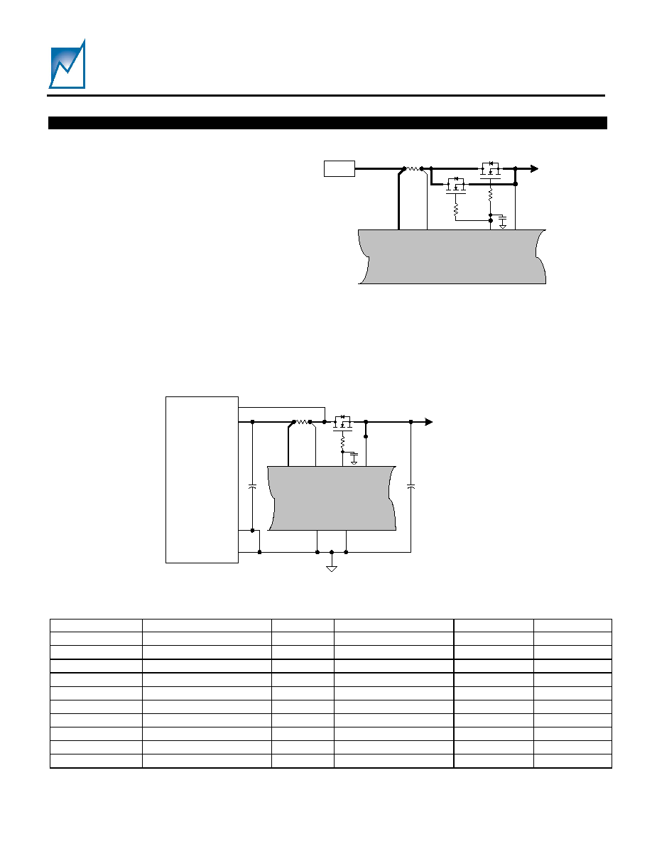
SMT4004A
Summit Microelectronics, Inc
2072 1.1 3/7/03
30
PARALLELING MOSFETS REDUCES VOLTAGE
DROPS AND POWER DISSIPATION
When supply regulation is unacceptable due to high
R
DS(ON)
two or more MOSFETs may be wired in
parallel to lower the R
DS(ON)
. For lower voltage
supplies with high current, such as a 1V supply
delivering 15A of load current, load regulation is
improved by using two or more MOSFETs in parallel.
The R
DS(ON)
is halved when two identical MOSFETs
are connected as in Figure 21. The MOSFET gates
must be connected with identical gate resistors.
REMOTE SENSING
This technique can be used with power supplies that
have Sense inputs. Remote sensing eliminates the
effect of the current sense resistor voltage drop. With
this arrangement (Figure 22) only the MOSFET R
DS(ON)
must be considered and a wider selection of devices
can be used.
SMT4004A
R
G1
10
VI
1
CB1
VG
A
T
E1
VO1
R
G2
10
Q1
Q2
V
IN
VOUT
to Application Circuit
R
S
C
G1
10nF
Figure 21. Parallel MOSFET Connections
SMT4004A
R
G1
10
VI
1
CB
1
VG
A
T
E
1
VO
1
Q1
DC-to-DC
Converter
VOUT
to Application Circuit
R
S
+V
SENSE
+V
FORCE
-V
SENSE
-V
FORCE
5x
220µF
100µF
PG
N
D
PG
N
D
C
G1
10nF
Figure 22. Remote Sense Connections
Table 3. Available Low R
DS(ON)
Power MOSFETs
Part Number
Manufacturer
V
(BR)DSS
R
DS(ON)
@ V
GS
= 10V
I
D
@100∞C Package
IRF3703 International
Rectifier
30V 2.8m
max.
180A Super
D2
IRF1404S International
Rectifier 40V
4m
max.
162A D2PAK
IRF6601 International
Rectifier
20V 3.8m
max.
20A DirectFET
TM
IRL3803S International
Rectifier 30V 6m
max.
140A D2PAK
HUF76145S3S Fairchild
Semiconductor 30V
4.5m
max.
75A D2PAK
HUF76145S3S Fairchild
Semiconductor 30V
5.5m
max.
75A D2PAK
STV160NF03L ST
Microelectronics
30V
2.8m
max.
113A Power
SO-10
STB80NF03L-04 ST
Microelectronics
30V
4m
max.
56A D2PAK
SUB75N03-04 Vishay
Siliconix
30V
4m
max.
75A TO-263
SUB75N04-05L Vishay
Siliconix
40V
5.5m
max.
55A TO-263
APPLICATIONS INFORMATION
(CONTINUED)
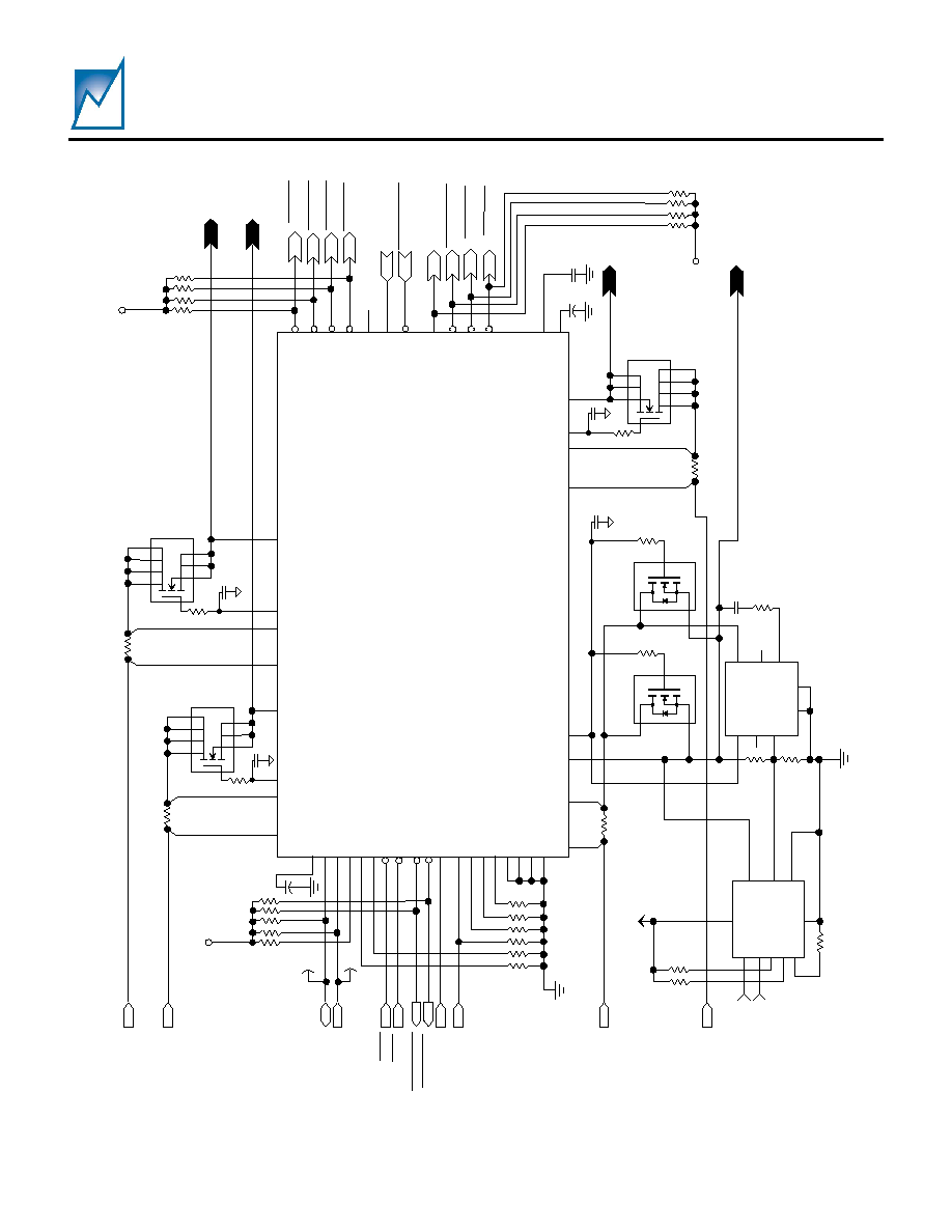
SMT4004A
Summit Microelectronics, Inc
2072 1.1 3/7/03
31
D
DD
S
D
SS
G
7
56
8
2
13
4
IR
F
7
8
0
5
S
M
T
4004A
A0
A1
A2
Me
mo
r
y
A
d
d
r
e
s
s
=
A
2
Reg
i
s
t
er
A
d
dr
es
s
=
9
2
SC
L
SDA
D
DD
S
D
SS
G
7
56
8
2
13
4
IR
F
7
8
0
5
bi
in
ou
t
33
0
W
a
t
c
h_
Lon
g_
D
o
g_
I
n
in
in
10
a
d
ju
s
t
v
a
l
u
e
f
o
r
c
u
r
r
e
n
t
tr
i
p
R
S
1
0.
00
2
a
d
j
u
st
va
l
u
e
f
o
r
cu
r
r
e
n
t
t
r
i
p
RS
2 0.
00
2
10
D
S
G
2
3
1
I
R
L3
80
3S
D
S
G
2
3
1
I
R
L3
80
3
S
VGAT
E3
CB3
VI3
VO3
LT14
31
3
4
1
2
7
8
56
V+
RT
O
P
CO
M
P
CO
L
L
E
C
T
O
R
RM
I
D
REF
GN
D
-
S
G
N
D
-
F
6.
8
1
K
2.
21
K
10
36
0
10
0.
1µ
F
D
DD
S
D
SS
G
7
56
8
2
13
4
IR
F
7
8
0
5
10
R
S
4 0.
00
2
a
d
j
u
st
va
l
u
e
f
o
r
cu
r
r
e
n
t
t
r
i
p
RS
3 0.
00
2
a
d
j
u
st
va
l
u
e
f
o
r
c
u
rr
e
n
t
t
r
i
p
VGAT
E4
CB4
VI4
VGAT
E1
CB1
VI1
VO1
VGAT
E2
CB2
VI2
VO2
in
in
3.
7V
1.
8
V
WL
D
I
WD
O
#
LDO
#
EN
A
B
L
E
PW
R
_
O
N
DG
ND
F
O
R
C
E_
SD
PGND
AG
N
D
PGN
D
UV
_
O
V
E
RRI
DE
in
ou
t
F
o
r
c
e
_
S
h
ut
do
wn_
I
n
in
in
in
W
a
t
c
h_
D
o
g_
O
u
t
L
o
n
g_Dog
_O
ut
SEAT
_
1
SE
AT
_
2
SEA
T
E
D2
#
SEA
T
E
D1
#
VR
E
F
H
1
VR
E
F
L
1
VO
U
T
1
5.
1V
2.
5
V
+5
V
(
V
cc)
+2.
5
V
+1
.
8
V
+3
.
3
V
VD
D
SC
L
SD
A
A0
A1
A2
GND
Vc
c
14
11
1
2
3
12
13
7
10
9
10
K
2p
l
c
s
33
0
Ou
t
Ou
t
Ou
t
Ou
t
RS
T
1
#
RS
T
2
#
RS
T
3
#
RS
T
4
#
CR
OW
B
A
R
Ou
t
Ou
t
Ou
t
Ou
t
5V
_R
S
T
3.
3V
_
R
S
T
2.
5V
_R
S
T
1.
8V
_R
S
T
NC
SM
P9
2
1
0
2_
W
i
r
e
_D
at
a
2_W
i
r
e
_
Cl
oc
k
SC
L
SD
A
SC
L
SDA
1
2
3
8
10
11
12
14
13
15
16
19
32
21
17
18
29
22
43
44
45
46
47
48
27
33
24
38
39
30
35
34
40
36
3
1
37
41
20
VGG
_
C
A
P
1u
F
28
10
K
+5
.
1
V
or
V
DD_
C
A
P
10
K
+5
.
1
V
or
V
DD_
C
A
P
I
R
Q
_
CLR#
MR
#
In
M
anu
al
_R
es
et
In
I
n
t
e
r
r
upt
_
C
l
ear
5
6
CBFA
U
LT
HE
A
L
T
H
Y
#
T
RKR
_
I
RQ
#
IR
Q
#
Ou
t
Ou
t
Ou
t
Ou
t
C
u
r
r
ent
_T
r
i
p
Pw
r
_
Sy
s
_
OK
TRK
R
_
I
RQ
PW
R
_
I
R
Q
7
9
26
25
10K
+5
.
1
V
or
V
DD_
C
A
P
VD
D_
C
A
P
10uF
42
VO4
23
4
1.
2
5
V
REF
0.
1µ
F
10
nF
10
nF
10
nF
1
0nF
Figure 23 ≠ IBM
TM
PowerNP NP4GS3 Network Processor Reference Platform. (Not all connections are shown.
Please contact IBM
TM
for further information)
.
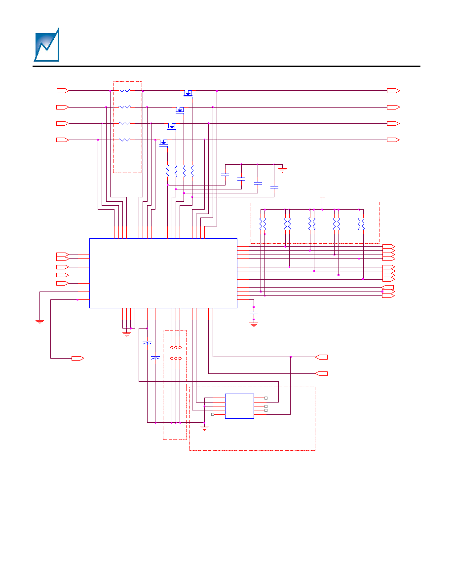
SMT4004A
Summit Microelectronics, Inc
2072 1.1 3/7/03
32
2.5VOUT
R3
Sense Resistor
Optional
Can be
shorted
C20
10nF
RST2#
R14
10K
C7
0.1uF
C21
10nF
25V
U1
SMT4004A
1
2
3
4
5
6
7
8
9
10
11
12
13
14
15
16
17 18
19
20 21 22
23
24
25
26
27
28
29
30
31
32
33
34 35
36 37
38
39
40
41
42
43
44 45
46 47
48
LDO#
WDO#
CROWBAR
1.25Vref
MR
#
IRQ_
CL
R#
IRQ#
P
G
ND1
TRKR_IRQ#
SEATED1#
SEATED2#
UV OVERIDE
RST1#
RST2#
RST3#
RST4#
P
G
ND2
DGND AGN
D
VO1 VO2
VO3 VO4
ENABLE
CBFAULT
HEALTHY#
FORCE SD
VGG CAP
VGATE4
VAGET3
VGATE2
VGATE1
PWR ON
CB
4
CB
3
CB
2
CB
1
VI
4
VI
3
VI
2
VI
1
V
DD CA
P
A0
A1 A2
SD
A
SC
L
WLDI
JP6
A0
1
2
FORCE SD
R11
10K
R8
10K
R9
10K
R2
Sense Resistor
Q4
MOSFET N
VDD_CAP
HEALTHY#
R17
10
25V
C1
1uF
PWR_ON
Optional SMX3200 Programmer
Connector - SDA/SCL
have 2K pullups
to +5V in the SMX3200
Q2
MOSFET N
R20
10
RST4#
IRQ#
SEATED1#
R6
10K
MR#
RST3#
1.8VIN
25V
C22
10nF
A0,A1,A2 have
internal 100k
pullups
WLDI
WDO#
JP4
A2
1
2
2.5VIN
3.3VIN
ENABLE
R13
10K
R18
10
External Pullups are only
needed if the output pins
drives other devices, otherwise
the pins can be left floating
5.0VIN
CROWBAR
RST1#
5.0VOUT
3.3VOUT
JP5
A1
1
2
SEATED2#
CBFAULT
R10
10K
R12
10K
J1
I2C
1
2
3
4
5
6
7
8
9
10
Gnd
SCL
Gnd3
SDA
Rsrv5
MR#
+10V
Rsrv8
+5V
Rsrv10
TRKR_IRQ#
R7
10K
IRQ_CLR#
R19
10
25V
R4
Sense Resistor
C19
10nF
Q3
MOSFET N
C2
10uF
1.8VOUT
R1
Sense Resistor
Q1
MOSFET N
R5
10K
25V
LDO#
Figure 24 ≠
Minimum External Component Requirements for an SMT4004A Application.
See application notes 20 and 25 for additional recommendations for operation in telecom systems or noisy environments.
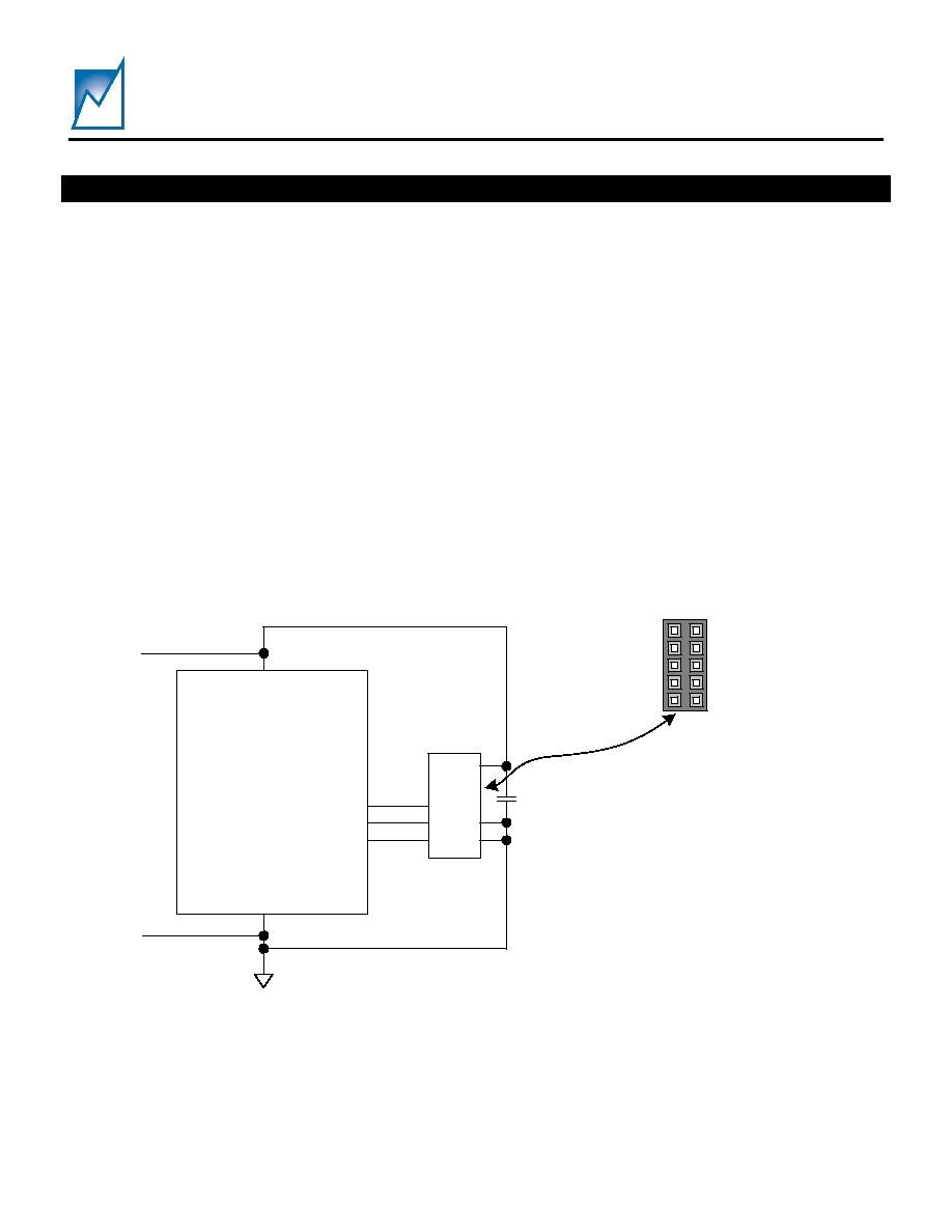
SMT4004A
Summit Microelectronics, Inc
2072 1.1 3/7/03
33
DEVELOPMENT HARDWARE AND SOFTWARE
The end user can obtain the Summit SMX3200
programming system for device prototype
development. The SMX3200 system consists of a
programming Dongle, cable and Windows GUI
software. It can be ordered on the website or from a
local Summit representative. The latest revisions of all
software and an Application Brief describing the
SMX3200 is available from the website
(
www.summitmicro.com
).
The SMX3200 programming Dongle/cable interfaces
directly between a PC's parallel port and the target
application. The SMT4004A is then configured on-
screen via an intuitive graphical user interface
employing drop-down menus.
The Windows GUI software will generate the data and
send it in I
2
C serial bus format so that it can be
directly downloaded to the SMT4004A via the
programming Dongle and cable. An example of the
connection interface is shown in Figure 25.
When design prototyping is complete the software can
generate a HEX data file that should be transmitted to
Summit for design verification and approval. Summit
will then assign a unique customer ID to the HEX code
and program production devices. The devices are
marked with the customer ID as a part number suffix
per the marking specification shown at the end of the
data sheet.
Please be aware that the end user can always
reconfigure a product that has been programmed by
Summit, however, doing so does not allow the part to
be fully tested with the new configuration register
settings.
Pin 9, 5V
Pin 7, 10V
Pin 5, Reserved
Pin 3, GND
Pin 1, GND
Pin 6, MR#
Pin 4, SDA
Pin 2, SCL
Pin 8, Reserved
Pin 10, Reserved
Top view of straight 0.1" x 0.1 closed-side
connector. SMX3200 interface cable connector.
9
7
5
3
1
10
8
6
4
2
SMT4004A
SDA
SCL
VDD_CAP
GND
0.1
F
Positive
Supply
Com m on
Ground
M R#
Figure 25 SMX3200 Programmer I
2
C Serial Bus Connections to Program the SMT4004A.
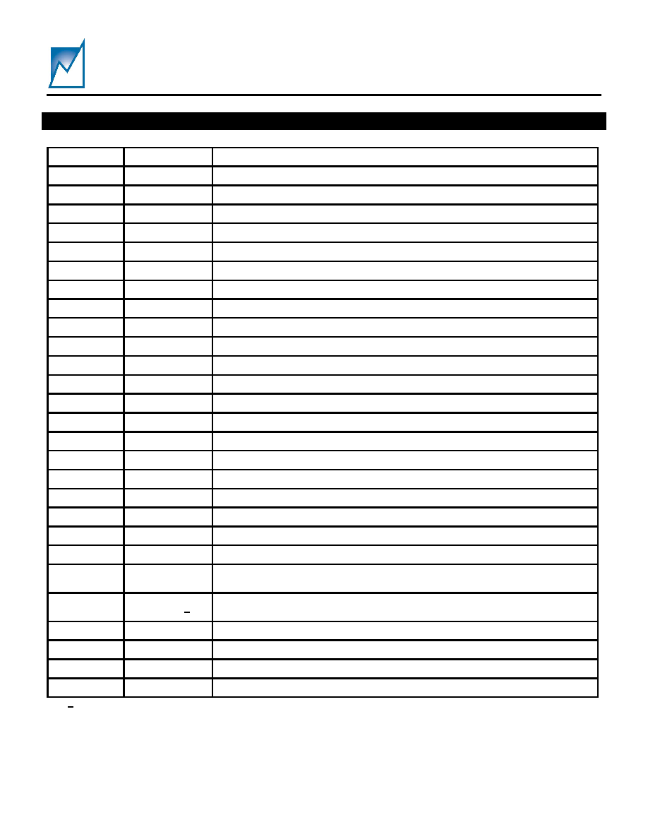
SMT4004A
Summit Microelectronics, Inc
2072 1.1 3/7/03
34
DEFAULT CONFIGURATION REGISTER SETTINGS ≠ SMT4004AF-181
Table 4
Note 1/ - Bits D5, D6 and D7 are reserved bits; therefore the contents of R18 may not be 00
h
.
The default device ordering number is SMT4004AF-181, is programmed as described above and tested over the
commercial temperature range.
Application Note 22 contains a complete description of the default settings and each
of the 32 individual Configuration Registers. The default configuration does not include Registers R16 and R17
(virtual addresses) or R1D, R1E and R1F (Fault Status Registers).
Register
Hex Contents
Configured as:
R00
B0
Bus-Side VI1 UV Threshold set to 4.424V - PVIT
UV
R01
50
Bus-Side VI2 UV Threshold set to 2.501V - PVIT
UV
R02
30
Bus-Side VI3 UV Threshold set to 1.860V - PVIT
UV
R03
20
Bus-Side VI4 UV Threshold set to 1.540V - PVIT
UV
R04
47
Bus-Side VI1 UV enabled , OV disabled, OV Threshold set to 6.548V - PVIT
OV
R05
4F
Bus-Side VI2 UV enabled , OV disabled, OV Threshold set to 4.502 - PVIT
OV
R06
4F
Bus-Side VI3 UV enabled , OV disabled, OV Threshold set to 3.348V - PVIT
OV
R07
4F
Bus-Side VI4 UV enabled , OV disabled, OV Threshold set to 2.772V - PVIT
OV
R08
B0
Card-Side VO1 Threshold set to 4.424V - PVOT
UV1
R09
50
Card-Side VO2 Threshold set to 2.501V - PVOT
UV1
R0A
30
Card-Side VO3 Threshold set to 1.860V - PVOT
UV1
R0B
20
Card-Side VO4 Threshold set to 1.540V - PVOT
UV1
R0C
CF
Card-Side VO1 Threshold 2 set to 3.759V - PVOT
UV2
R0D
CF
Card-Side VO2 Threshold 2 set to 2.125V - PVOT
UV2
R0E
8F
Card-Side VO3 Threshold 2 set to 1.580V - PVOT
UV2
R0F
8F
Card-Side VO4 Threshold 2 set to 1.309V - PVOT
UV2
R10
05
Responds to pin biased addresses, 1010
BIN
, 250V/s slew rate on and off
R11
88
Enable RST# source VOX-UV1
R12
88
Enable RST# source VOX-UV1
R13
00
Disable all IRQ# sources
R14
00
Disable all IRQ# sources
R15
E0
800 ms POR to IRQ# delay, disable all QT-CBX IRQ# Triggers
CB Trip point set to 50mV
R18
40
- Note 1/
MR# Required to Program, Fault Latching disabled, I
2
C Power On/Off
Disabled, OV does not cause a Forced ShutDown
R19
00
Disable all Crowbar sources
R1A
00
Disable Quicktrip Threshold on all manager channels
R1B
00
All outputs active low, over current delay 25µs
R1C
C0
Reset 200ms, Longdog off, Watchdog off
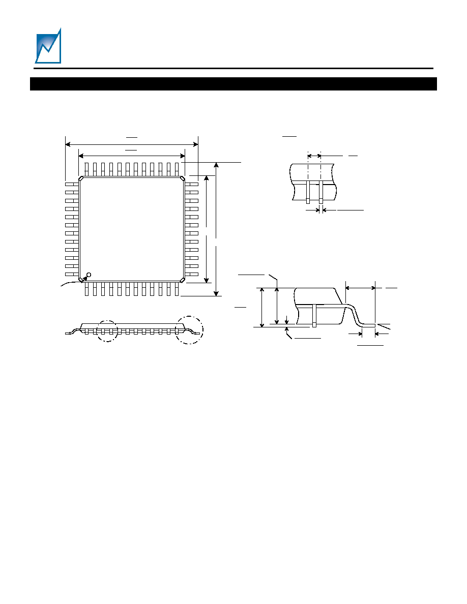
SMT4004A
Summit Microelectronics, Inc
2072 1.1 3/7/03
35
PACKAGE
A
B
Pin 1
Indicator
Inches
(Millimeters)
0.002 - 0.006
(0.05-0.15)
MAX.
0.047
(1.2)
0.037 - 0.041
0.95 - 1.05
0.018 - 0.030
(0.45 - 0.75)
0.039
(1.00)
0.02
(0.5)
BSC
0.007 - 0.011
(0.17 - 0.27)
DETAIL "A"
DETAIL "B"
(B)
(A)
(A)
0.354
(9.00) BSC
0.276
(7.00)
BSC (B)
48 PIN TQFP PACKAGE
0
o
Min to
7
o
Max
Ref Jedec M S-026
Ref
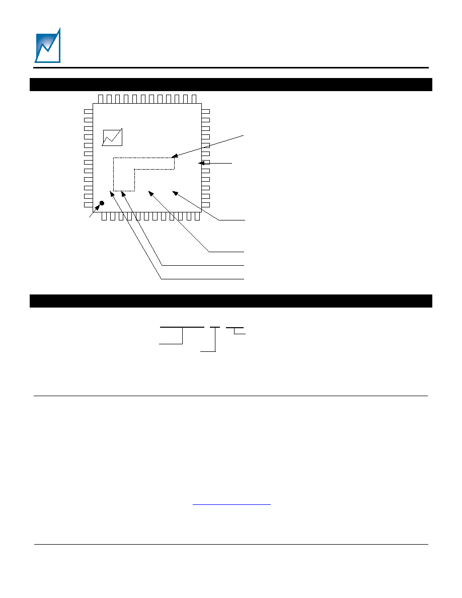
SMT4004A
Summit Microelectronics, Inc
2072 1.1 3/7/03
36
PART MARKING
SUMMIT
SMT4004AF
AYYWW
Pin 1
Annn
Summit Part Number
Date Code (YYWW)
Lot tracking code (Summit use)
Drawing not to scale
xx
Status Tracking Code
(Blank, MS, ES, 01, 02,...)
(Summit Use)
Product Tracking Code (Summit use)
Part Number suffix
(Contains Customer specific ordering requirements)
ORDERING INFORMATION
NOTICE
SUMMIT Microelectronics, Inc. reserves the right to make changes to the products contained in this publication in order to improve design,
performance or reliability. SUMMIT Microelectronics, Inc. assumes no responsibility for the use of any circuits described herein, conveys no license
under any patent or other right, and makes no representation that the circuits are free of patent infringement. Charts and schedules contained
herein reflect representative operating parameters, and may vary depending upon a user's specific application. While the information in this
publication has been carefully checked, SUMMIT Microelectronics, Inc. shall not be liable for any damages arising as a result of any error or
omission.
SUMMIT Microelectronics, Inc. does not recommend the use of any of its products in life support or aviation applications where the failure or
malfunction of the product can reasonably be expected to cause any failure of either system or to significantly affect their safety or effectiveness.
Products are not authorized for use in such applications unless SUMMIT Microelectronics, Inc. receives written assurances, to its satisfaction, that:
(a) the risk of injury or damage has been minimized; (b) the user assumes all such risks; and (c) potential liability of SUMMIT Microelectronics, Inc.
is adequately protected under the circumstances.
Revision 1.1 - This document supersedes all previous versions and covers Status Tracking Code 13 and Windows GUI revision 3.3.0 and later.
Please check the Summit Microelectronics, Inc. web site at
www.summitmicro.com
for data sheet updates.
© Copyright 2003 SUMMIT MICROELECTRONICS, Inc.
Power Management for CommunicationsTM
I2C is a trademark of Philips Corporation.
IBM, the IBM logo, PowerPC, and PowerPC 750 are trademarks of International Business Machines in the United States and/or other countries.
TRAKKING
TM
and TRAKKER
TM
are trademarks of Summit Microelectronics, Inc.,
SMT4004A F nnn
Package
F=48 Lead TQFP
Summit Part Number
Part Number Suffix (see page 34)
Specific requirements are contained in the suffix
such as Commercial or Industrial Temp Range,
Hex code, Hex code revision, etc.